

Page 1
Rayson
®
Bluetooth
Module
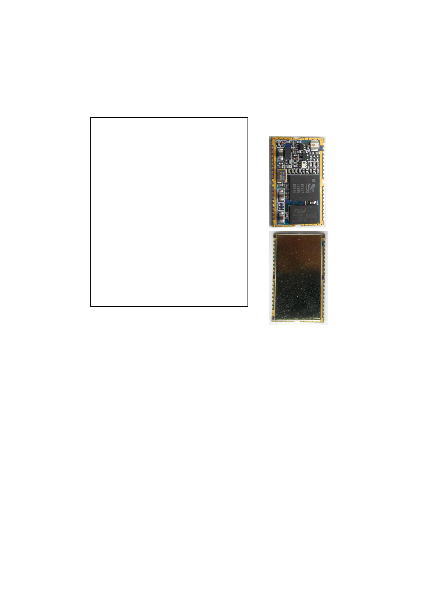
Class1 BC04-ext Module BTM-220
Features
■ Bluetooth Ver. 2.0 compliant
■ Transmit Power up to +18dBm(class1)
■ Low current consumption:
Hold, Sniff, Park, Deep sleep mode
■ 2.7V to 3.6V operation
■ Full Bluetooth Data rate over UART and USB
■ Support up to 7 ACL links and 3 SCO links
■ Enhanced Data Rate(EDR) compliant
with Ver.0.9 of specification for both 2Mbps
and 3Mbps modulation modes
■ Interface: USB, UART&PCM( for voice codec)
■ HCI or SPP firmware is available
■ Mini outline: 28.2 X 15.0 X 2.8 mm
● Laptop and Desktop PCs
● Access point
● Domestics and Industrial applications
● Personal Digital Assistants(PDA)
● Serial Adapter
● GPS, POS, Barcode Reader
● Digital camera, Printer& Cellular phone
● Cordless handset
Application
Outline
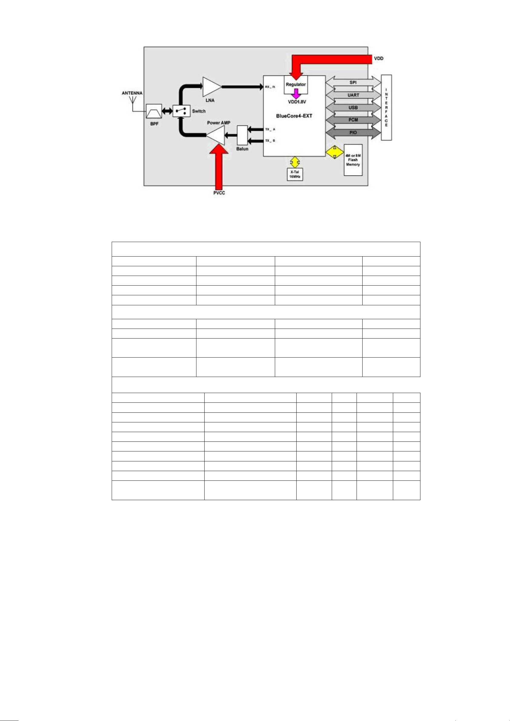
Block Diagram
Page 2
Electrical Characteristics
Absolute Maximum Ratings
Parameter Min. Max. Unit
Storage Temperature -40 +85 ℃
Supply Voltage(VDD) 2.7 3.6 DCV
Supply Voltage(PVCC) 3.0 3.3 DCV
Other Pin Voltage Vss-0.4 VDD+0.4 DCV
Recommended Operating Conditions
Parameter Min. Max. Unit
Temperature -10 +70
Supply Voltage for
UART
Supply Voltage for
USB
General Electrical Specification
Parameter Description Min. Typ. Max. Unit
Carrier Frequency 2.402 2.480 GHz
RF Output Power Measured in 50ohm 15 16.5 18 dBm
RX sensitivity - -88 -85 dBm
Load Impedance No abnormal Oscillation 5:1
Input Low Voltage RESET,UART,GPIO,PCM -0.30 - 0.80 DCV
Input High Voltage RESET,UART,GPIO,PCM 0.7VDD - VDD+0.3 DCV
Output Low Voltage UART,GPIO,PCM - - 0.40 DCV
Output High Voltage UART,GPIO,PCM VDD-0.4 - - DCV
Average Current
Consumption
Receive DM1 114 mA
3.0 3.6 DCV
3.0 3.6 DCV
℃
Page 3
Radio Characteristics - Basic Data Rate
Transmitter , VDD = 3.3V Temperature =+20°C
Frequency
(GHz)
RF transmit power
2.402 15 16.5 18 dBm
2.441 15 16.5 18 dBm
2.480 15 16.5 18
Initial carrier frequency
tolerance
2.402 - 12 25 kHz
2.441 - 10 25 kHz
2.480 - 9 25
-20dB bandwidth for
modulated carrier
2.402 - 890 1000 kHz
2.441 - 870 1000 kHz
2.480 - 820 1000
Carrier Frequency Drift
(single slot packet DH1)
2.402 - ±10 ±20 kHz
2.441 - ±10 ±20 kHz
2.480 - ±10 ±20
Carrier Frequency Drift (five
slot packet DH5)
2.402 - ±10 ±20 kHz
2.441 - ±10 ±20 kHz
2.480 - ±10 ±20
Drift Rate
2.402 - ±7 ±14 kHz/50µs
2.441 - ±7 ±14 kHz/50µs
2.480 - ±7 ±14
Min. Typ. Max. Bluetooth
Specification
-6 to +20
±75
1000
<
25
<
40
<
20
<
Unit
dBm
kHz
kHz
kHz
kHz
kHz/50µs
RF power control range 16 25 - >16 dB
avg
△f1
“Maximum
Modulation”
maz
△f2
“Minimum
Modulation”
Adjacent channel transmit power F=F0±2MHz
Adjacent channel transmit power F=F0±3MHz
Adjacent channel transmit power F>F0 +3MHz
Adjacent channel transmit power F<F0 -3MHz
2.402 145 165 170 kHz
2.441 145 165 170 kHz
140<△f1
2.480 145 165 170
2.402 115 150 - kHz
2.441 115 150 - kHz
2.480 115 150 -
- -35 -20
- -45 -40
- -50 -40
- -50 -40
>115
- 20
<
- 40
<
- 40
<
- 40
<
avg
<175
kHz
kHz
dBm
dBm
dBm
dBm
Receiver , VDD = 3.3V Temperature =+20°C
Frequency
(GHz)
Sensitivity at 0.1% BER
2.402 - -87 -85 dBm
2.441 - -87 -85 dBm
(Single slot packets)
Sensitivity at 0.1% BER
2.480 - -87 -85
2.402 - -87 -85 dBm
2.441 - -87 -85 dBm
(Multi slot packets)
Maximum received signal
level at 0.1% BER
2.480 - -87 -85
2.402 -20 -10 - dBm
2.441 -20 -10 - dBm
2.480 -20 -10 C/I co-channel - 6 11 < 11 dB
Adjacent channel selectivity C/I F=F0 +1 MHz - -4 Adjacent channel selectivity C/I F=F0 - 1MHz - -4 -
Min. Typ. Max. Bluetooth
Specification
- 70
<
- 70
<
- 20
>
0
<
0
<
Unit
dBm
dBm
dBm
dB
dB
Page 4

Adjacent channel selectivity C/I F=F0 +2 MHz - -38 Adjacent channel selectivity C/I F=F0 - 2MHz - -23 Adjacent channel selectivity C/I F>=F0 +3 MHz
Adjacent channel selectivity C/I F<=F0 -5 MHz
Adjacent channel selectivity C/I F=F
image
- -45 -
- -44 -
- -22 F0 = 2441 MHz
Maximum level of intermodulation interference
-30 > -39 dBm
(n=5)
Radio Characteristics – Enhanced Data Rate
Transmitter , VDD = 3.3V Temperature =+20°C
<
- 30
- 20
<
< - 40
< - 40
< - 9
dB
dB
dB
dB
dB
Frequency
(GHz)
Maximum RF transmit power
2.402 15 16.5 18 dBm
2.441 15 16.5 18 dBm
2.480 15 16.5 18
Min. Typ. Max. Bluetooth
Specification
-6 to +20
Unit
dBm
Relative transmit power - -1.2 - -4 to +1 dB
π/4 DQPSK
Maximum carrier frequency stability w
π/4 DQPSK
Maximum carrier frequency stability w
π/4 DQPSK
Maximum carrier frequency stability | w
8 DPSK
Maximum carrier frequency stability w
8 DPSK
Maximum carrier frequency stability w
8 DPSK
Maximum carrier frequency stability | w
π/4 DQPSK
Modulation Accuracy
RMS DVEM -
99% DEVM -
Peak DEVM 8 DPSK
Modulation Accuracy
RMS DVEM -
99% DEVM -
Peak DEVM In-band spurious emissions
F>F0 +3 MHz
0
i
+ wi |
0
0
i
+ wi |
0
- 2 -
- 6 -
- 8 -
- 2 -
- 6 -
- 8 -
7
13
19
7
13
17
- <-50 F<F0 -3 MHz - <-50 F=F0 -3 MHz - -46 F=F0 -2 MHz - -34 F=F0 -1 MHz - -35 F=F0 +1 MHz - -35 F=F0 +2 MHz - -31 -
+3 MHz - -33 -
F=F
0
EDR Differential Phase Encoding No
- < 20 %
- < 30 %
- <
- < 13 %
- < 20 %
- <
> 99 %
±10 for all blocks
<
±75 for all packets
<
±75 for all blocks
<
< ±10 for all blocks
±75 for all packets
<
±75 for all blocks
<
35 %
25 %
< -40
-40
<
-40
<
-20
<
-26
<
-26
<
-20
<
-40
<
kHz
kHz
kHz
kHz
kHz
kHz
dBm
dBm
dBm
dBm
dBm
dBm
dBm
dBm
Errors
Receiver , VDD = 3.3V Temperature =+20°C
Modulation Min. Typ. Max. Bluetooth
Specification
Sensitivity at 0.1% BER
π/4 DQPSK
- -87 8 DPSK - -78 -
< -70
-70
<
Unit
dBm
dBm
Page 5

Maximum received signal level at
0.1% BER
C/I co-channel at 0.1% BER
Adjacent channel selectivity C/I
+1 MHz
F=F
0
Adjacent channel selectivity C/I
-1 MHz
F=F
0
Adjacent channel selectivity C/I
+2 MHz
F=F
0
Adjacent channel selectivity C/I
-2 MHz
F=F
0
Adjacent channel selectivity C/I
+3 MHz
F=F
0
Adjacent channel selectivity C/I
-5 MHz
F=F
0
F0 = 2405, 2441, 2477 MHz
Adjacent channel selectivity C/I
F=F
image
π/4 DQPSK
- -8 8 DPSK - -10 π/4 DQPSK
- 10 8 DPSK - 19 π/4 DQPSK
- -10 8 DPSK - -5 π/4 DQPSK
- -11 8 DPSK - -5 π/4 DQPSK
- -40 8 DPSK - -40 π/4 DQPSK
- -23 8 DPSK - -20 π/4 DQPSK
- -45 8 DPSK - -45 π/4 DQPSK
- -45 8 DPSK - -45 -
π/4 DQPSK
-20
8 DPSK -15
> -20
-20
>
< +13
+21
<
< 0
+5
<
< 0
+5
<
< -30
-25
<
< -20
-13
<
< -40
-33
<
< -40
-33
<
< -7
0
<
dBm
dBm
dB
dB
dB
dB
dB
dB
dB
dB
dB
dB
dB
dB
dB
dB
dB
dB
Page 6

BTM-220 Pin Function
Pin No. Pin Name Pin Type Description
1 GND GND
2 PVCC Power
3 AIO(0) Bi-directional
4 AIO(1) Bi-directional
5 PIO(0) Bi-directional
6 PIO(1) Bi-directional
7 PIO(2) Bi-directional
8 PIO(3) Bi-directional
9 PIO(4) Bi-directional
10 GND GND
11 PIO(5) Bi-directional
12 PIO(6) Bi-directional
13 PIO(7) Bi-directional
14 PIO(8) Bi-directional
15 PIO(9) Bi-directional
16 RESET CMOS input
17 VCC Power
18 GND GND
19 GND GND
20 USB_DP Bi-directional
21 USB_DN Bi-directional
22 PCM_SYNC Bi-directional
23 PCM_IN CMOS input
24 PCM_OUT CMOS output
25 PCM_CLK Bi-directional
26 UART_RX CMOS input
27 UART_TX CMOS output
28 UART_RTS CMOS output
29 GND GND
30 UART_CTS CMOS input
31 SPI_MOSI CMOS input
32 SPI_CSB CMOS input
33 SPI_CLK CMOS input
34 SPI_MISO CMOS output
35 PIO(11) Bi-directional
36 PIO(10) Bi-directional
37 RF_IO Analogue
38 GND GND
Common ground
Power Amp. Power Supply(3.3V)
Programmable I/O terminal
Programmable I/O terminal
Programmable I/O terminal, RX Enable
Programmable I/O terminal, TX Enable
Programmable I/O terminal, USB_PULL_UP
Programmable I/O terminal, USB_WAKE_UP
Programmable I/O terminal, USB_ON
Common ground
Programmable I/O terminal, USB_DETACH
Programmable I/O terminal, CLK_REQ
Programmable I/O terminal
Programmable I/O terminal
Programmable I/O terminal
Reset input of module, Active low reset
Module power supply input
Common ground
Common ground
USB data plus
USB data minus
Synchronous data sync
Synchronous data input
Synchronous data output
Synchronous data clock
UART data input
UART data output
UART request to send(active low)
Common ground
UART clear to send(active low)
Serial Peripheral Interface data input
Chip select for Synchronous Serial Interface(active
low)
Serial Peripheral Interface clock
Serial Peripheral Interface data output
Programmable I/O terminal
Programmable I/O terminal
Antenna interface
Common ground
Page 7

BTM-220 Dimension
 Loading...