

Page 1

BR9080AF-W / BR9080ARFV-W / BR9080ARFVM-W /
Memory ICs
BR9016AF-W / BR9016ARFV-W / BR9016ARFVM-W
8k, 16k bit EEPROMs for direct
connection to serial ports
BR9080AF-W / BR9080ARFV-W / BR9080ARFVM-W /
BR9016AF-W / BR9016ARFV-W / BR9016ARFVM-W
The BR9080A and BR9016A series are serial EEPROMs that can be connected directly to a serial port and can be
erased and written electrically. Writing and reading is performed in word units, using four types of operation commands.
Communication occurs though CS, SK, DI, and DO pins, WC pin control is used to initiate a write disabled state, enabling
these EEPROMs to be used as one-time ROMs. During writing, operation is checked via the internal status check.
!Applications
Movie, camera, cordless telephones, car stereos, VCRs, TVs, DIP switches, and other battery-powered equipment
requiring low voltage and low current
!Features
1) BR9080AF-W / ARFV-W / ARFVM-W (8k bit) : 512 words ×16 bits
BR9016AF-W / ARFV-W / ARFVM-W (16k bit) : 1024 words × 16bits
2) Single power supply operation
3) Serial data input and output
4) Automatic erase-before-write
5) Low current consumption
Active (5V) : 5mA (max.)
Standby (5V) : 3µA (ma x.)
6) Noise filter built into SK pin
7) Write protection when V
Inhibition on inadvertant write with the WC pin.
8) SOP8 / SSOP-B8 / MSOP8
9) High reliability CMOS process
10) 100,000 ERASE / WRITE cycles
11) 10 years Data Retention
CC is low
1/12
Page 2
Memory ICs
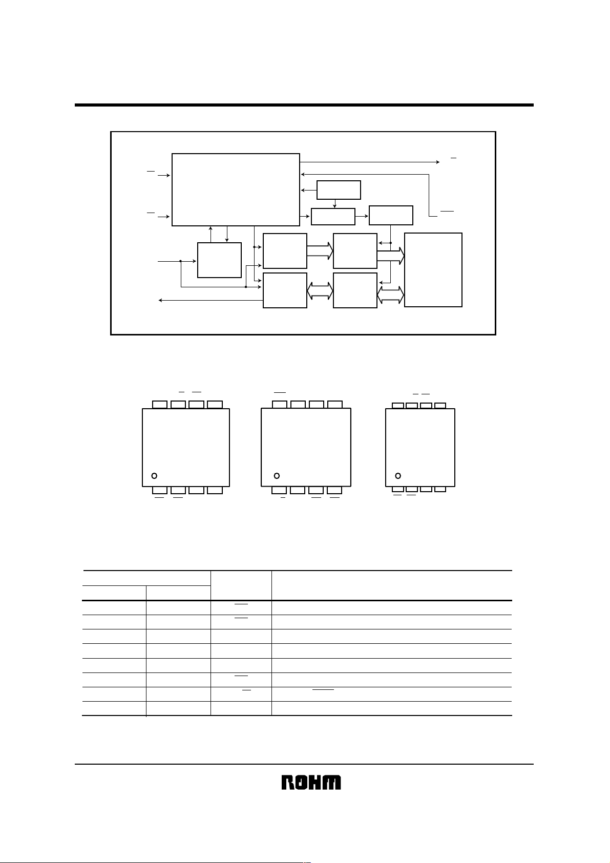
!!!!Block diagram
BR9080AF-W / BR9080ARFV-W / BR9080ARFVM-W /
BR9016AF-W / BR9016ARFV-W / BR9016ARFVM-W
CS
SK
DI
DO
!!!!Pin descriptions
INSTRUCTION DECODE
CONTROL
CLOCK GENERATION
CC
R / B WC GND
V
INSTRACTION
REGISTER
ADD
BUFFER
DATA
REGISTER
WC GND DO DI
∗
9bit
16bit
DETECT
SUPPLY
VOLTAGE
WRITE
DISABLE
ADD
DECORDER
R / W
AMPS
HIGH
VOLTAGE
GENERATOR
∗
9bit
16bit
V
CC
R / B
WC
∗
8,192 bit
EEPROM
∗ BR9016A is 10bit, 16,384bit
BR9080A is 9bit, 8,192bit
GND
R / B WC
MSOP / SSOP
1
2
3
4
5
6
7
8
CS SK
BR9080ARFVM
BR9016ARFVM
Pin No.
SOP
3
4
5
6
7
8
1
2
DI
: MSOP8
DO
Pin name
CS
SK
DI
DO
GND
WC
R / B
CC
V
CS SKR / B V
CC
BR9080AF
BR9016AF
: SOP8
BR9080ARFV
BR9016ARFV
Fig.1
Function
Chip Select Control
Serial Data Clock Input
Op code, address, Serial Data Input
Serial Data Output
Ground 0V
Write Control Input
READY / BUSY Output
Power supply
CS SK
DI
DO
: SSOP-B8
2/12
Page 3
BR9080AF-W / BR9080ARFV-W / BR9080ARFVM-W /
Memory ICs
!!!!Absolute maximum ratings (Ta=25°C)
Supply voltage
Power dissipation
Storage temperature
Operation temperature
Input voltage
∗
1 Reduced by 4.5mW for each increase in Ta of 1°C over 25°C.
∗2
Reduced by 3.0mW for each increase in Ta of 1°C over 25°C.
∗3
Reduced by 3.1mW for each increase in Ta of 1°C over 25°C.
!!!!Recommended operating conditions (Ta=25°C)
Power supply voltage
Input voltage
BR9016AF-W / BR9016ARFV-W / BR9016ARFVM-W
Parameter Symbol Limits Unit
V
CC
SOP8
Pd
Tstg
Topr
−−0.3∼V
Parameter Symbol
WRITE
READ
V
V
SSOP-B8
MSOP8
Min.
CC
IN
−0.3∼+7.0 V
1
∗
450
2
∗
300
3
∗
310
−65∼+125 °C
−40∼+85 °C
CC
+0.3 V
Typ. Max. Unit
2.7
2.7
0
− 5.5 V
− 5.5 V
− V
CC
mW
V
3/12
Page 4
BR9080AF-W / BR9080ARFV-W / BR9080ARFVM-W /
Memory ICs
!!!!Electrical characteristics
BR9080AF-W / ARFV-W / ARFVM-W, BR9016AF-W / ARFV-W / ARFVM-W : 5V
(Unless otherwise noted, Ta=−40∼85°C, V
Parameter Symbol Min. Typ. Max. Unit Conditions
Input low level voltage 1
Input high level voltage 1
Input low level voltage 2
Input high level voltage 2
Output low level voltage
Output high level voltage
Input leak current
Output leak current
Operating current
Standby current
SK frequency
BR9080AF-W / ARFV-W / ARFVM-W, BR9016AF-W / ARFV-W / ARFVM-W : 3V
(Unless otherwise noted, Ta=−40∼85°C, V
Parameter Symbol Min. Typ. Max. Unit Conditions
Input low level voltage 1
Input high level voltage 1
Input low level voltage 2
Input high level voltage 2
Output low level voltage
Output high level voltage
Input leak current
Output leak current
Operating current
Standby current
SK frequency
Not designed for radiation resistance
BR9016AF-W / BR9016ARFV-W / BR9016ARFVM-W
CC=2.7V∼5.5V)
DI pin
V
V
DI pin
V
CS, SK, WC pin
V
CS, SK, WC pin
V
OL
=2.1mA
I
V
IOH=−0.4mA
µA
IN
=0V∼V
V
µA
V
f
SK
mA
mA
SK
f
µA
CS / SK / DI / WC=VCC DO, R / B=OPEN
CC
OUT
=0V∼VCC, CS=V
=2MHz tE / W=10ms (WRITE)
=2MHz (READ)
MHz
DI pin
V
V
DI pin
V
CS, SK, WC pin
V
CS, SK, WC pin
V
OL
=100µA
I
V
IOH=−100µA
µA
IN
=0V∼V
V
µA
V
f
SK
mA
mA
SK
f
µA
CS / SK / DI / WC=VCC DO, R / B=OPEN
CC
OUT
=0V∼VCC, CS=V
=2MHz tE / W=10ms (WRITE)
=2MHz (READ)
MHz
V
V
V
V
V
V
I
I
V
V
V
V
V
V
I
I
I
I
CC1
CC2
I
f
I
I
CC1
CC2
I
f
IL1
IH1
IL2
IH2
OL
OH
LI
LO
SB
SK
IL1
IH1
IL2
IH2
OL
OH
LI
LO
SB
SK
−−
0.7×V
CC
−
0.8×V
CC
0
VCC−0.4
−1
−1
−
−
−
−
CC=2.7V∼3.3V)
−−
0.7×V
CC
−
0.8×V
CC
0
VCC−0.4
−1
−1
−
−
−
−
CC
0.3×V
−
−
−
0.2×V
CC
−
−
0.4
−
V
CC
−
1
−
1
−
5
−
3
−
−
3
2
−
CC
0.3×V
−
−
−
0.2×V
CC
−
−
0.4
−
V
CC
−
1
−
1
−
3
−
0.75
−
−
2
2
−
CC
−
CC
−
4/12
Page 5

BR9080AF-W / BR9080ARFV-W / BR9080ARFVM-W /
Memory ICs
!!!!Operating timing characteristics
BR9080AF-W / ARFV-W / ARFVM-W, BR9016AF-W / ARFV-W / ARFVM-W
(Unless otherwise noted, Ta=−40∼85°C, V
CS setup time
CS hold time
Data setup time
Data hold time
DO rise delay time
DO fall delay time
Self-timing programming cycle
CS minimum high level time
READY / BUSY display valid time
Time when DO goes HIGH-Z (via CS)
Data clock high level time
Data clock low level time
Write control setup time
Write control hold time
!!!!Timing chart
Synchronous Data Input Output Timing
BR9016AF-W / BR9016ARFV-W / BR9016ARFVM-W
CC=2.7V∼5.5V)
Parameter Symbol Min. Typ. Max. Unit
CSS
100 −−ns
f
CSH
100 −−ns
t
100 −−ns
DIS
t
100 −−ns
t
DIH
t
PD1
t
PD0
E / W
t
t
t
t
OH
t
WH
WL
t
t
WCS
WCH
t
CS
−−150 ns
−−150 ns
−−10 ms
250 −−ns
CS
−−150 ns
SV
0 − 150 ns
230 −−ns
230 −−ns
0 −−ns
0 −−ns
t
CS
t
t
CSS
SK
DI
DO
WC
· Input data are clocked in to DI at the rising edge of the clock (SK).
· Output data will toggle on the falling edge of the SK clock.
· The WC pin does not have any effect on the READ, EWEN and EWDS operations.
t
WL
t
DIS
t
PD
WH
t
DIH
t
PD
Fig.2
t
CSH
t
OH
5/12
Page 6

BR9080AF-W / BR9080ARFV-W / BR9080ARFVM-W /
Memory ICs
!!!!Circuit operation
(1) Command mode
BR9080A
Read (READ)
Write (WRITE)
Write enable (WEN)
Write disable
∗ : Means either VIH or V
Address and data are transferred from LSB.
BR9016A
Read (READ)
Write (WRITE)
Write enable (WEN)
Write disable
∗ : Means either VIH or VIL
Address and data are transferred from LSB.
(2) Writing enabled / disabled
1) When CS is “HIGH” during power up, BR9080AF-W / ARFV-W / ARFVM-W, BR9016AF-W / ARFV-W / ARFVM-W
comes up in the write disabled (WDS) state. In order to be programmable, it must receive a write enable (WEN)
instruction.
The device remains programmable until a disable (WDS) instruction is entered, or until it is powered down.
2) It is unnecessary to add the clock after 16th clock.
BR9016AF-W / BR9016ARFV-W / BR9016ARFVM-W
Instruction Start Bit Op Code Address Data
1010 100 A0 A1 A2 A3 A4 A5 A6 A7 A8
D0 D1 − D14 D15
(WDS)
1010 010 A0
1010 0011
1010 0000
IL
A1 A2 A3 A4 A5 A6 A7 A8
∗ ∗ ∗ ∗ ∗ ∗ ∗ ∗
∗ ∗ ∗ ∗ ∗ ∗ ∗ ∗
Instruction Start Bit Op Code Address Data
1010 10 A0 A1 A2 A3 A4 A5 A6 A7 A8 A9
D0 D1 − D14 D15
(WDS)
1010 01 A0 A1
1010 0011
1010 0000
A2 A3 A4 A5 A6 A7 A8 A9
∗ ∗ ∗ ∗ ∗ ∗ ∗ ∗
∗ ∗ ∗ ∗ ∗ ∗ ∗ ∗
H
SK
CS
DI
DO
R / B
WC
L
H
L
H
L
H
1
1
HIGH-Z
High or LOW
48
01 000
Fig.3
ENABLE = 11
DISABLE = 00
12 16
6/12
Page 7
BR9080AF-W / BR9080ARFV-W / BR9080ARFVM-W /
Memory ICs
(3) Read cycle
BR9080AF-W / ARFV-W / ARFVM-W
BR9016AF-W / BR9016ARFV-W / BR9016ARFVM-W
H
SK
CS
DI
DO
R / B
WC
L
H
L
H
L
H
High or LOW
1
01 1000
1
HIGH-Z
4
8163248
CS
t
STANDBY
A1 A7 A8
A0
D0
D15 D15D0
Read Data (n) Read Data (n+1)
HIGH-Z
t
OH
Fig.4 BR9080AF-W / ARFV-W / ARFVM-W
BR9016 AF-W / ARFV-W / ARFVM-W
H
SK
CS
DI
DO
R / B
WC
L
H
L
H
L
H
High or LOW
1
01 100
1
HIGH-Z
4
Fig.5 BR9016AF-W / ARFV-W / ARFVM-W
8163248
A0
A2
A1
A8 A9
D0
D15 D15D0
Read Data (n) Read Data (n+1)
CS
t
STANDBY
HIGH-Z
t
OH
1) After the fall of the 16th clock pulse, 16-bit data is output from the DO pin in synchronization with the falling edge of the
SK signal.
(DO output changes at a time lag of t
During the t
PD0 and tPD1 timing, the tPD time should be assured before data is read, to avoid the previous data being lost.
PD0, tPD1 because of internal circuit delay following the falling edge of the SK signal.
See the synchronized data input / output timing chart in Fig.2.)
2) The data stored in the next address is clocked out of the device on the falling edge of 32nd clock. The data stored in
the upper address every 16 clocks is output sequentially by the continual SK input. Also the read operation is reset by
CS High.
7/12
Page 8

BR9080AF-W / BR9080ARFV-W / BR9080ARFVM-W /
Memory ICs
(4) Write cycle
BR9080AF-W / ARFV-W / ARFVM-W
BR9016AF-W / BR9016ARFV-W / BR9016ARFVM-W
H
SK
CS
DI
DO
R / B
WC
L
H
L
H
L
H
14 8 1632
01 00 1 0 A0 A1 A7 A8 D0 D15
1
HIGH-Z
t
WCS
t
CS
HIGH-Z
t
SV
t
E-W
t
WCH
Fig.6 BR9080AF-W / ARFV-W / ARFVM-W
BR9016 AF-W / ARFV-W / ARFVM-W
H
SK
CS
DI
DO
R / B
WC
L
H
L
H
L
H
14 8 1632
01 00 1 A0 A1 A2 A8 A9 D0 D15
1
HIGH-Z
t
SV
t
WCS
Fig.7 BR9016AF-W / ARFV-W / ARFVM-W
t
WCH
t
CS
HIGH-Z
t
E-W
1) At the rising edge of 32nd clock, R / B pin will be come out “LOW” after the specified time delay (tSV).
2) From above edge R / B will indicate the ready / busy status of the chip: “LOW” indicated programming is all in
progress: “HIGH” indicates the write cycle is complete and this part is ready for another instruction.
3) During the input of Write command, CS must be “LOW”. However, once the write operation started, CS could be either
“HIGH” or “LOW”.
4) If WC becomes “HIGH” during Write Cycle, the write operation is halted. In this case, the address data in writing is no
guaranteed. It is necessary to rewrite it.
8/12
Page 9

BR9080AF-W / BR9080ARFV-W / BR9080ARFVM-W /
Memory ICs
(5) READY / BUSY display
(R / B pin and DO pin: BR9080AF-W / ARFV-W / ARFVM-W, BR9016AF-W / ARFV-W / ARFVM-W)
1) This display outputs the internal status signal; the R / B pin outputs the HIGH or LOW status at all times. The display
can also be output from the DO pin. Following completion of the writing command, if CS falls while SK is LOW, either
HIGH or LOW is output. (The display can also be output without using the R / B pin, leaving it open.)
2) When writing data to a memory cell, the READY / BUSY display is output from the rise of the 32nd clock pulse of the
SK signal after tSV, from the R / B pin.
R / B display = LOW: writing in progress
(The internal timer circuit is activated, and after the tE / W timing has been created, the timer circuit stops automatically.
Writing of data to the memory cell is done during the tE / W timing, during which time other commands cannot be
received.)
R / B display = HIGH: command standby state
(Writing of data to the memory cell has been completed and the next command can be received.)
BR9016AF-W / BR9016ARFV-W / BR9016ARFVM-W
CS
SK
DI
DO
R / B
READY
Clock
Write command
HIGH-Z
t
PD
BUSY
BUSY
Fig.8 R / B Status Output timing chart
1) DO will output R / B status after CS is held low during SK=L, until CS is held high.
Note : The document may be strategic technical data subject to COCOM regulations.
READY
READY
t
OH
HIGH-Z
9/12
Page 10

BR9080AF-W / BR9080ARFV-W / BR9080ARFVM-W /
Memory ICs
!!!!Operation notes
(1) Turning the power supply on and off
1) When the power supply is turned on and off, CS should be set to HIGH (=V
2) When CS is LOW, the command input reception state (active) is entered. If the power supply is turned on in this state,
erroneous operations and erroneous writing can occur because of noise and other factors. To avoid this, make sure
CS is set to HIGH (=V
(Good example) Here, the CS pin is pulled up to V
(Bad example) CS is LOW when the power supply is turned on or off.
BR9016AF-W / BR9016ARFV-W / BR9016ARFVM-W
CC).
CC) before turning on the power supply.
CC.
When turning off the power supply, wait at least 10msec before turning it on again. Failing to
observe this condition can result in the internal circuit failing to be reset when the power supply is
turned on.
In this case, because CS remains LOW, the EEPROM may perform erroneous operations or
write erroneous data because of noise or other factors.
* Please be aware that the case shown in this example can also occur if CS input is HIGH-Z.
V
CC
V
CC
GND
CC
V
CS
GND
Good example Bad example
Fig.9
(2) Noise countermeasures
1) SK noise
If noise occurs at the rise of the SK clock input, the clock is assumed to be excessive, and this can cause malfunction
because the bits are out of alignment.
2) WC noise
During a writing operation, noise at the WC pin can be erroneously judged to be data, and this can cause writing to be
forcibly interrupted.
3) V
CC noise
Noise and surges on the power supply line can cause malfunction. We recommend installing a bypass capacitor
between the power supply and ground to eliminate this problem.
10/12
Page 11

Memory ICs
BR9016AF-W / BR9016ARFV-W / BR9016ARFVM-W
(3) Canceling modes
1) Read commands
BR9080AF-W / BR9080ARFV-W / BR9080ARFVM-W /
SK
CS
DI
DO
WC HIGH or LOW
Cancellation method: CS HIGH
2) Write commands
SK
CS
Start bit
4 bits 4 bits 8 bits
Operating code Address
Cancel can be performed for the entire read mode space
32 Clock
32 Clock
Fig.10
16 bits
DataDO D15
DI
R / B
WC
Operating code
Start bit
4 bitsc4 bits 8 bits 16 bits
Address Data
DO D15
Fig.11
tE / W
dba
Canceling methods
a : Canceled by setting CS HIGH. The WC pin is not involved.
b : If the WC pin goes HIGH for even a second, writing is forcibly interrupted. Cancellation occurs even if the CS pin is
HIGH. At this point, data has not been written to the memory, so the data in the designated address has not yet
been changed.
c : The operation is forcibly canceled by setting the WC pin to HIGH or turning off the power supply (although we do
not recommend using this method). The data in the designated address is not guaranteed and should be written
once again.
d : If CS is set to HIGH while the R / B signal is HIGH (following the tE / W timing), the IC is reset internally, and waits
for the next command to be input.
11/12
Page 12

BR9080AF-W / BR9080ARFV-W / BR9080ARFVM-W /
Memory ICs
!!!!External dimension (Units : mm)
BR9016AF-W / BR9016ARFV-W / BR9016ARFVM-W
BR9080ARFVM-W
BR9016ARFVM-W
BR9080ARFV
BR9016ARFV
6.4 ± 0.3
(0.52)
BR9080AF
BR9016AF
2.9±0.1
58
0.1
4.0±0.2
0.475
0.9Max.
0.75±0.05
±
2.8
41
0.22
0.65
0.08±0.05
+0.05
−0.04
0.08 S
0.29±0.15
0.145
0.6±0.2
+0.05
−0.03
M
0.08
MSOP8 SOP8
3.0 ± 0.2
548
4.4 ± 0.2
1
0.22 ± 0.1
1.15 ± 0.1
0.1
0.65
0.3Min.
0.15 ± 0.1
0.1
SSOP-B8
4.4 ± 0.2
6.2 ± 0.3
1.5 ± 0.1
0.11
5.0 ± 0.2
85
41
1.27
0.4 ± 0.1
0.15 ± 0.1
0.3Min.
0.15
12/12
 Loading...