

Page 1

Memory IC
BR9010-W / F-W / FV-W / RFV-W / RFVM-W / BR9020-W / F-W / FV-W /
RFV-W / RFVM-W / BR9040-W / F-W / FV-W / RFV-W / RFVM-W
1k, 2k, 4k, bit EEPROMs for direct
connection to serial ports
BR9010-W / BR9010F-W / BR9010FV-W /
BR9010RFV-W / BR9010RFVM-W
BR9020-W / BR9020F-W / BR9020FV-W /
BR9020RFV-W / BR9020RFVM-W
BR9040-W / BR9040F-W / BR9040FV-W /
BR9040RFV-W / BR9040RFVM-W
The BR90XX series a re ser ial EE PROMs tha t can be con nected di r ectl y to a se rial port a nd can be e ras ed and wri tten
electrically. Writing and reading is per fomed in word units, using fou r types of operation commands. Communication
occurs through CS, SK, DI, and DO pins, WC pin control is used to initiate a write disabled state, enabling these
EEPROMs to be used as on e-time ROM s. During wri ting opera tion is ch ecked vi a the intern al status ch eck.
Application
zzzz
General-Purpose
Features
z
1) BR9010-W / F-W / FV-W / RFV-W / RFVM-W (1k bit) : 64 words×16bit
BR9020-W / F-W / FV-W / RFV-W / RFVM-W (2k bit) : 128words×16bit
BR9040-W / F-W / FV-W / RFV-W / RFVM-W (4k bit) : 256words×16bit
2) Single power supply.
3) Serial data I/O.
4) Self-timed programming cycle with auto-erase.
5) Low supply current.
Active (5V) : 2mA (max.)
Standby (5V) : 3µA (max.) (CMOS INPUT)
6) Noise filter on the SK pin. Write protection when the supply is low.
7) Write pro tectio n by WC pin.
8) Space Saving DIP8/SO P8/SSOP -B8/MS OP8pin Pa ckage s.
9) 100,000 erase/ write cycles endurance.
10) Provide 1 0 years of date rete ntion.
11) Easy connection to serial port.
12) “FFFFh” stored in all address on shipped.
1/14
Page 2
Memory IC
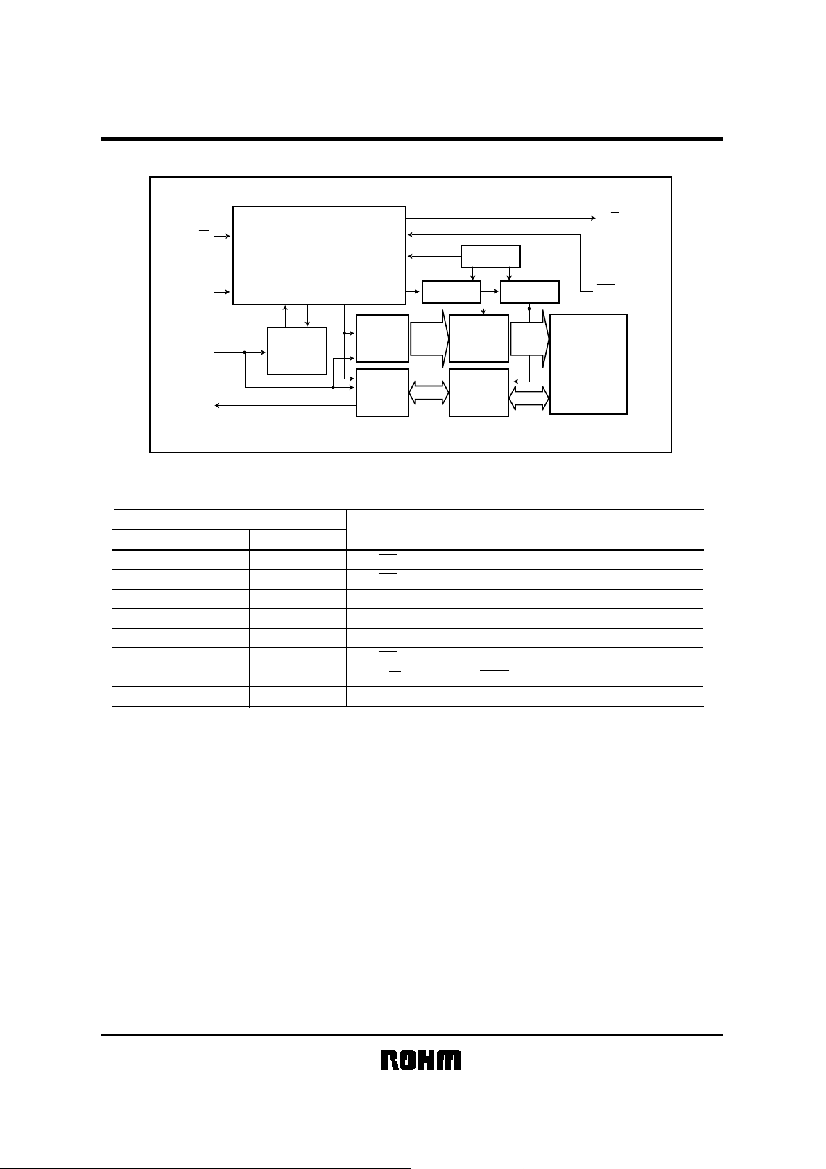
Block diagram
zzzz
T erminal Function
zzzz
BR9010-W / F-W / FV-W / RFV-W / RFVM-W / BR9020-W / F-W / FV-W /
CS
SK
DI
DO
Pin No.
BR90xx-W/RFV-W/RFVM-W
1
2
3
4
5
6
7
8
RFV-W / RFVM-W / BR9040-W / F-W / FV-W / RFV-W / RFVM-W
R / B
Command decode
Control
Clock generation
Command
register
BR90xxF-W/FV-W
3
4
5
6
7
8
1
2
Address
buffer
Data
register
Pin name
CS
SK
DI
DO
GND
WC
R / B
CC
V
6bit
7bit
8bit
BR9010
BR9020
BR9040
16bit
Power supply
voltage detector
R / W
High voltage
generator
6bit
BR9010
7bit
BR9020
8bit
BR9040
16bit
1,024bit
2,048bit
4,096bit
EEPROM
array
Write disable
Address
decoder
amplifier
Function
Chip Select Input
Serial Date Clock Input
Serial Date Input (Op code, address)
Serial Date Output
Ground (0V)
Write Control Input
READY/ BUSY Status Output
Power Supply
WC
BR9010
BR9020
BR9040
2/14
Page 3
Memory IC
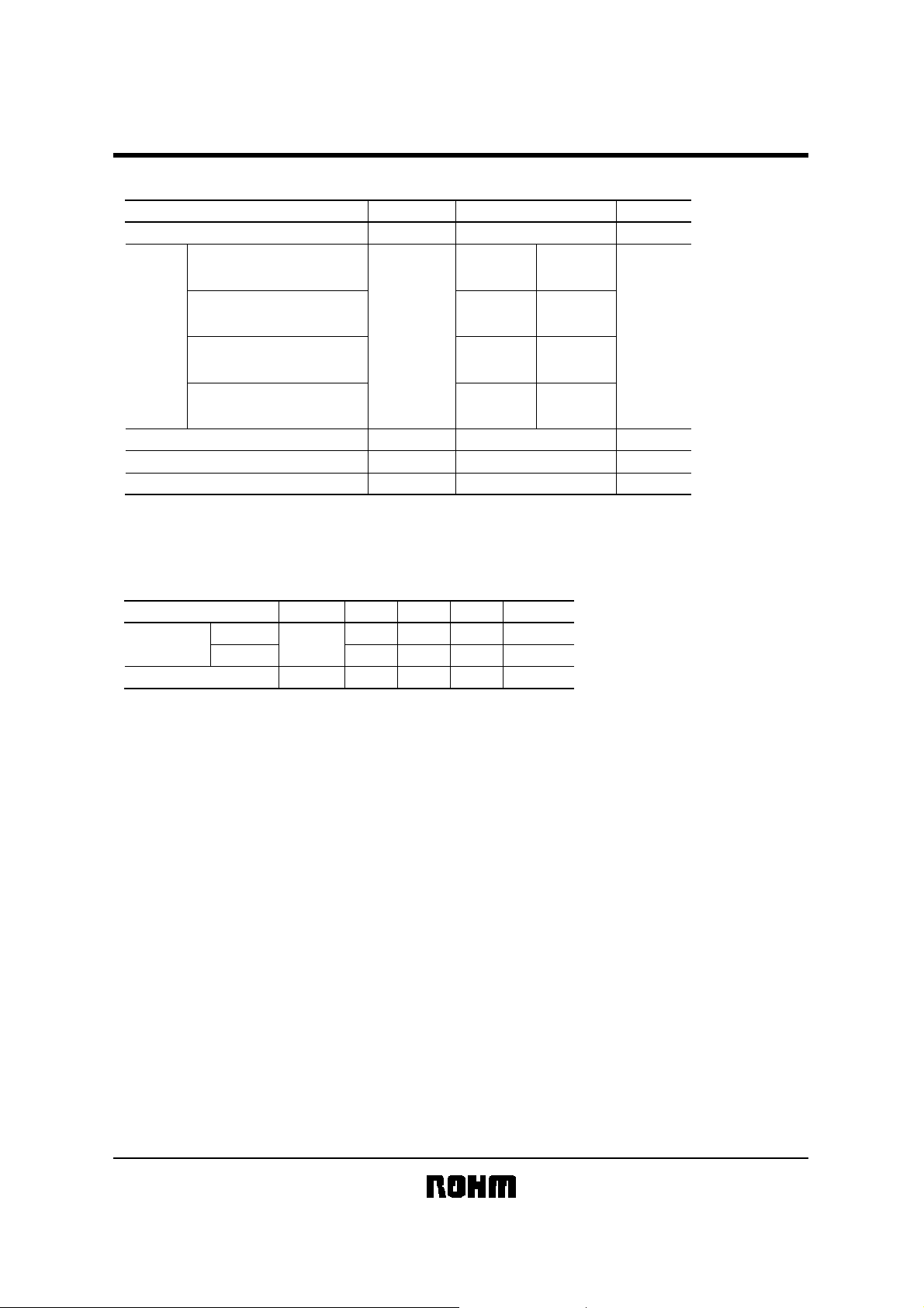
Absolute Maximum Ratings
zzzz
BR9010-W / F-W / FV-W / RFV-W / RFVM-W / BR9020-W / F-W / FV-W /
RFV-W / RFVM-W / BR9040-W / F-W / FV-W / RFV-W / RFVM-W
(Ta=25°C)
Parameter
Symbol
Supply Voltage
BR9010-W,
BR9020-W,
BR9040-W
BR9010F-W,
BR9020F-W,
Power
dissipation
BR9040F-W
BR9010FV-W, BR9010RFV-W,
BR9020FV-W, BR9020RFV-W,
BR9040FV-W, BR9040RFV-W
BR9010RFVM-W,
BR9020RFVM-W,
BR9040RFVM-W
Storage Temperature
Operating Temperature
Terminal Voltage
∗1 Degradation is done at 8.0mW/˚C for operation above Ta=25˚C
∗2 Degradation is done at 4.5mW/˚C for operation above Ta=25˚C
∗3 Degradation is done at 3.0mW/˚C for operation above Ta=25˚C
∗4 Degradation is done at 3.1mW/˚C for operation above Ta=25˚C
CC
V
Pd
Tstg
Topr
−
DIP8
SOP8
SSOP-B8
MSOP8
−0.3∼V
Limits
−0.3∼+7.0
−65∼+125
−40∼+85
CC
+0.3
800
450
300
310
Unit
V
1
∗
2
∗
mW
3
∗
4
∗
°C
°C
V
Recommended Operating Condition
zzzz
Parameter Symbol Min. Typ. Max. Unit
Supply voltage
Input voltage
Write
Read
CC
V
V
IN
(Ta=25°C)
2.7
2.0
0
− 5.5 V
− 5.5 V
− V
CC
V
3/14
Page 4
Memory IC
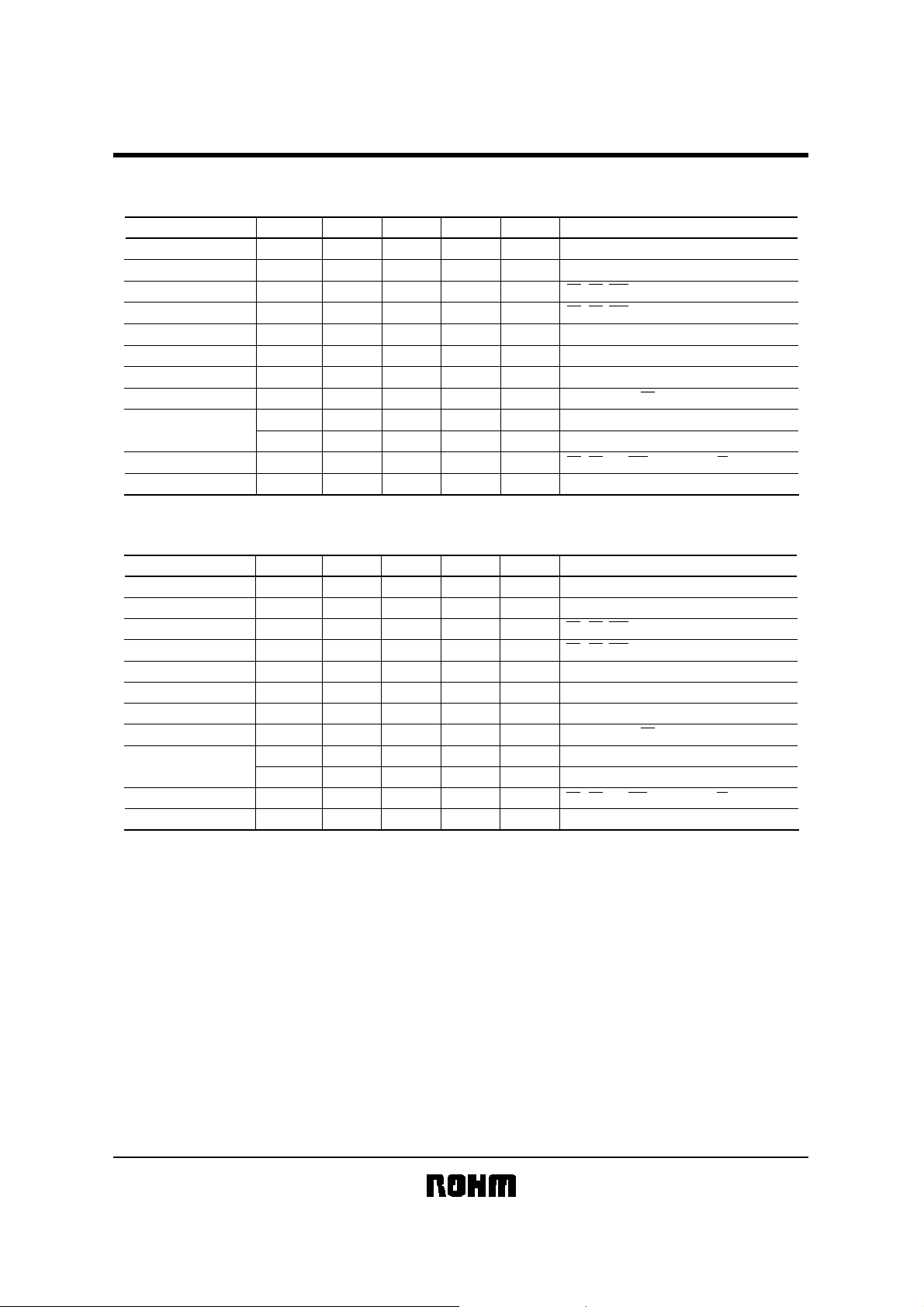
Electrical Characteristics
zzzz
BR9010-W / F-W / FV-W / RFV-W / RFVM-W / BR9020-W / F-W / FV-W /
RFV-W / RFVM-W / BR9040-W / F-W / FV-W / RFV-W / RFVM-W
Unless otherwise specified ( T a=−40~+85°C, V
Parameter
Input LOW Voltage 1
Input HIGH Voltage 1
Input LOW Voltage 2
Input HIGH Voltage 2
Output LOW Voltage
Output HIGH Voltage
Input Leakage Current
Output Leakage Current
Operating Current
Standby Current
Clock Frequency
Symbol
V
IL1
V
IH1
V
IL2
V
IH2
V
OL
V
OH
I
LI
I
LO
I
CC1
I
CC2
I
SB
f
SK
Min. Typ. Max. Unit Conditions
−
CC
0.7×V
−
CC
0.8×V
0
CC
−0.4
V
−1
−1
−
−
−
−
Unless otherwise specified ( T a=−40~+85°C, V
Parameter
Input LOW Voltage 1
Input HIGH Voltage 1
Input LOW Voltage 2
Input HIGH Voltage 2
Output LOW Voltage
Output HIGH Voltage
Input Leakage Current
Output Leakage Current
Operating Current
Standby Current
Clock Frequency
Symbol
V
IL1
V
IH1
V
IL2
V
IH2
V
OL
V
OH
I
LI
I
LO
I
CC1
I
CC2
I
SB
f
SK
Min. Typ. Max. Unit Conditions
−
0.7×V
CC
−
0.8×V
CC
0
V
CC
−0.4
−1
−1
−
−
−
−
CC
=
2.7V~5.5V)
−
−
−
−
−
−
−
−
−
−
−
−
CC
=
2.7V~3.3V)
−
−
−
−
−
−
−
−
−
−
−
−
0.3×V
−
0.2×V
−
0.4
V
1
1
2
1
3
2
0.3×V
−
0.2×V
−
0.4
V
1
1
1.5
0.5
2
2
DI pin
V
CC
DI pin
V
CS, SK, WC pin
V
CC
CS, SK, WC pin
V
V
OL
=2.1mA
I
CC
CC
V
OH
=−0.4mA
I
IN
=0V∼V
V
µA
V
µA
SK
f
mA
f
mA
SK
CS, SK, DI, WC=VCC, DO, R / B=OPEN
µA
MHz
DI pin
V
CC
DI pin
V
CS, SK, WC pin
V
CC
CS, SK, WC pin
V
V
OL
I
V
I
OH
V
µA
µA
V
f
mA
mA
SK
f
SK
CS, SK, DI, WC=VCC, DO, R / B=OPEN
µA
MHz
CC
OUT
=0V∼VCC, CS=V
CC
=2MHz, tE / W=10ms (WRITE)
=2MHz (READ)
−
=100µA
=−100µA
IN
=0V∼V
CC
OUT
=0V∼VCC, CS=V
CC
=2MHz, tE / W=10ms (WRITE)
=2MHz (READ)
−
4/14
Page 5

Memory IC
AC Oper ation Char act erist ics
zzzz
( Ta=−40~+85°C, V
BR9010-W / F-W / FV-W / RFV-W / RFVM-W / BR9020-W / F-W / FV-W /
RFV-W / RFVM-W / BR9040-W / F-W / FV-W / RFV-W / RFVM-W
CC
=
2.7~5.5V)
Parameter Symbol Min. Typ. Max. Unit
Chip Select Setup Time
Chip Select Hold Time
Data In Setup Time
Data In Hold Time
Delay to Output High
Delay to Output Low
Self-Timed Program Cycle
Minimum Chip Select High Time
Data Output Disable Time( From
CS)
Clock High Time
Clock Low Time
Write Control Setup Time
Write Control Hold Time
Clock High to Output READY/BUSY Status
t
t
t
t
CSS
CSH
DIS
DIH
PD1
PD0
E / W
CS
OH
WH
WL
WCS
WCH
SV
100
100
100
100
−−
−−
−−
−−
−−
−−
−−
250
230
230
0
0
0
−−
−
−−
−−
−−
−−
−−
ns
ns
nst
nst
150 nst
150 nst
10 mst
nst
150 nst
nst
nst
ns
ns
150 nst
5/14
Page 6

BR9010-W / F-W / FV-W / RFV-W / RFVM-W / BR9020-W / F-W / FV-W /
Memory IC
I / O Circuit
zzzz
(1) Input Circuit
RESET int.
RFV-W / RFVM-W / BR9040-W / F-W / FV-W / RFV-W / RFVM-W
CS int.
CS
CS int.
DI
(2) Output Circuit
SK
WC
DO
OE int.
R/B
6/14
Page 7

Memory IC
Operating
zzzz
BR9010-W / F-W / FV-W / RFV-W / RFVM-W / BR9020-W / F-W / FV-W /
RFV-W / RFVM-W / BR9040-W / F-W / FV-W / RFV-W / RFVM-W
(1) Instruction Code
Instruction
READ
WRITE
Write Enable (WEN)
Write Disable (WDS)
Address and data must be transferred from LSB.
∗ Means either V
BR9020-W/F-W/FV-W/RFV-W/RFVM-W ∗1= "0"
BR9010-W/F-W/FV-W/RFV-W/RFVM-W ∗1, 2= "0"
IH
or V
IL
Start Bit Op Code
1010 1000
1010 0100
1010 0011
1010 0000
Synchronous Data Input Output Timing
CS
t
CSS
SK
DI
t
WL
t
DIS
Address
A0 A1 A2 A3 A4 A5 (
A0 A1 A2 A3 A4 A5 (
A6)∗2 (A7)∗1
A6)∗2 (A7)∗1
D0 D1−D14 D15
D0 D1−D14 D15
Data
(READ DATA)
(WRITE DATA)
∗ ∗ ∗ ∗ ∗ ∗ ∗ ∗
∗ ∗ ∗ ∗ ∗ ∗ ∗ ∗
t
CS
t
WH
t
DIH
t
CSH
t
t
PD
DO
WC
Input Data is clocked into the DI pin on the rising edge of the clock SK
Output data is clocked out on the falling edge of the SK clock.
The WC pin does not have any affect on the READ, WEN and WDS operations.
Between instructions, CS must be brought High for greater than the minimum of
CS
. If CS is maintained Low, the next instruction isn't detected.
t
PD
Fig.1
t
OH
7/14
Page 8

Memory IC
(2) WRITE Enable / Disable
SK
CS
DI
DO
R / B
BR9010-W / F-W / FV-W / RFV-W / RFVM-W / BR9020-W / F-W / FV-W /
RFV-W / RFVM-W / BR9040-W / F-W / FV-W / RFV-W / RFVM-W
H
L
H
L
H
L
H
1
1
01 000
High-Z
48
ENABLE = 11
DISABLE = 00
12 16
WC
HIGH or LOW
Fig.2
1) When power is first applied, the device has been held in a reset status, with respect to the write enable, in the same
way the write disable (WDS) instruction is executed. Before the write instruction is executed, the device must be
received the write ena ble (WEN) instruction. Once the device is done, th e device remains programm able until the
write disable (WDS) instruction is executed or the supply is removed from the device.
2) It is unnecessary to add the clock after 16
th clock. If the device is recieved the clock, the device ignores the clock.
3) As both of the enable and disable instruc tio ns don ’ t depend o n t he status o f the WC pin, the state of W C isn ’ t cared
during the instruction.
4) The instruction is recognized after th e risi ng ed ge of 8 th clock for t he addres s foll o wing 8 cloc ks fo r the o pcode, but
the specified address isn’t cared during the instructions.
8/14
Page 9

BR9010-W / F-W / FV-W / RFV-W / RFVM-W / BR9020-W / F-W / FV-W /
Memory IC
RFV-W / RFVM-W / BR9040-W / F-W / FV-W / RFV-W / RFVM-W
(3) Read Cy cle
SK
CS
DI
DO
R / B
WC
SK
CS
DI
DO
R / B
WC
H
L
H
L
H
L
H
HIGH or LOW
H
L
H
L
H
L
H
HIGH or LOW
1
01 10000
1
HIGH-Z
1
01 10000
1
HIGH-Z
4
Fig.3 BR9010-W / F--W / FV-W / RFV-W / RFVM-W
4
Fig.4 BR9020-W / F-W / FV-W / RFV-W / RFVM-W
81632
CS
t
A0 A5 00
D0 D15 D15D0
Read Data (n) Read Data (n+1)
8163248
A0 A6 0
D0
D15 D15D0
Read Data (n) Read Data (n+1)
STANDBY
HIGH-Z
CS
t
STANDBY
HIGH-Z
t
OH
t
OH
H
SK
CS
DI
DO
R / B
WC
L
H
L
H
L
H
HIGH or LOW
1
01 10 000
1
HIGH-Z
4
Fig.5 BR9040-W / F-W / FV-W / RFV-W / RFVM-W
81632
A0 A6 A7
D0
D15 D15D0
Read Data (n) Read Data (n+1)
t
CS
STANDBY
HIGH-Z
t
OH
1) On the falling edge of 16 th clock, the data stored in the specified address (n) is clocked out of the DO pin.
The Output DO is toggled after the internal propagation t
is the previous data or unstable, and to take in the data, t
PDO or tPD1
on the falling edge of SK. During t
PD
is needed. (Refer to Fig.1 Synchronous data input output
PD0
or t
PD1,
the data
timing.)
2) The data stored in the next address is clocked out of the device on the falling edge of 32nd clock. The data stored in
the upper address every 16 clocks is output sequentially by the continual SK input. Also the read operation is reset by
CS High.
9/14
Page 10

BR9010-W / F-W / FV-W / RFV-W / RFVM-W / BR9020-W / F-W / FV-W /
Memory IC
RFV-W / RFVM-W / BR9040-W / F-W / FV-W / RFV-W / RFVM-W
(4) Write Cycle
SK
CS
DI
DO
R / B
WC
SK
CS
DI
DO
R / B
WC
H
L
H
L
H
L
H
H
L
14 8 1632
1
01 00 1 00 00A0 A5 D0 D15
High-Z
t
E/W
t
SV
t
WCS
t
CS
High-Z
t
WCH
Fig.6 BR9010-W / F-W / FV-W / RFV-W / RFVM-W
H
L
H
L
H
L
H
H
L
14 8 1632
01 00100 0A0 A6 D0 D15
1
High-Z
t
E/W
t
SV
t
WCS
t
CS
High-Z
t
WCH
SK
CS
DI
DO
R / B
WC
Fig.7 BR9020-W / F-W / FV-W / RFV-W / RFVM-W
H
L
H
L
H
L
H
H
L
14 8 1632
01 00 1 0 0 A0 A6 A7 D0 D15
1
High-Z
t
E/W
t
SV
t
WCS
t
CS
High-Z
t
WCH
Fig.8 BR9040-W / F-W / FV-W / RFV-W / RFVM-W
10/14
Page 11

Memory IC
BR9010-W / F-W / FV-W / RFV-W / RFVM-W / BR9020-W / F-W / FV-W /
RFV-W / RFVM-W / BR9040-W / F-W / FV-W / RFV-W / RFVM-W
1) During the write in struc tion , CS must be br ought Low. However once the write op eratio n start ed, CS may be eith er
High or Low. But in the case of connecting the W C pin to the CS pi n. CS and WC must b e brought Low during
programming cycle.(If the WC pin is brought High during the write cycle, the write operation is halted. In that case, the
data of the specified address is not guaranteed. It is necessary to rewrite it.)
2) After the R / B pin changed Busy to Ready, once CS is brought Hi gh, then CS keep Low ,which means the status of
being able to accept a n inst ructi on. The de vice c an take i n the input from SK and DI, but in t he case of keeping CS
Low without being brought High once, the input is canceled until being CS High once.
3) At the rising edge of 32 nd clock, the R / B pin will be driven Low after the specified time delay (tSV).
4) During programming, R / B is tied to Low by the device (On the rising edge of SK taken in the last data (D15), internal
timer starts and automatically finished after the data of memory cell is written spending tE / W. SK could be either High
or Low at the time.
5) After input writ e instruction, also the DO pin will be able to show the status of R / B, in the case that CS is falling from
High to Low while SK is tied to Low. (Refer to READY / BUSY STA TUS in the next page.)
(5) READY / BUSY ST A TUS (on the R / B pin, the DO pin)
1)The DO pin outputs the READY / BUSY status of the internal part, which shows whether the device is ready to receive
the next inst ruction or not. (Hi gh or Low )
After the write instruction is compl eted, if CS is b rought from high to l ow while SK is Low, the DO pin outputs the
internal status. (The R / B pin may be no connection.
2) When written to the memory cell, R / B status is output after tSV spent from the rising edge of 32 th clock on SK.
R / B =Low : under writing
After spending tE / W operating the internal timer, the device automatically finishes writing.
During tE / W, the memory array is accessed and any instruction is not received.
R / B=High : ready
Auto programming has been completed. The device is ready to receive the next Instruction.
SK
CS
DI
DO
R / B
READY
CLOCK
WRITE INSTRUCTION
HIGH-Z
t
PD
BUSY
BUSY
READY
READY
t
OH
HIGH-Z
Fig.9 R / B Status Output Timing
11/14
Page 12

Memory IC
BR9010-W / F-W / FV-W / RFV-W / RFVM-W / BR9020-W / F-W / FV-W /
RFV-W / RFVM-W / BR9040-W / F-W / FV-W / RFV-W / RFVM-W
(6) About the direct connection between the DI and DO pins
The device can be used with the DI pin connected to the DO pin directly.
But when the READY / BUSY status is output, be careful about the bus conflict on the port of the controller.
Attention to Use
zzzz
(1) Power ON / OFF
1) The CS is brought High during power–up and power–down.
2) This device is in active state while CS is Low.
3) The extrao rd i nary functi o n or data coll ap s e m ay o c cu r in that cond it ion becau se of n o ise etc, if power–up and power–
down is done wi th CS brou ght Low.
In order to prevent above errors from happening, keep CS High during power-up and power-down.
(Good example) CS is brought High during power–up and power-down.
Please take more than 10ms between power–up and power-off, or the internal circuit is not always
reset.
(Bad example) CS is brought Low during power–up and power-down.
The CS pin is always Low in this case, the noise may force the device to make malfunction or
inadvertent write.
It sometimes occurs in the case that the CS pin is Hi-Z.
V
CC
V
CC
GND
CC
V
CS
GND
Good Bad
Fig.10
(2) Noise Rejection
1) SK NOISE
If SK line has a lot of noise for rising time of SK, the device may recognize the noise as a clock and then clock will be
shifted.
2) WC NOISE
If WC line has noise during write cycle (tE / W), there may be a chance to deny the programming.
3) VCC NOISE
It recommended tha t capacitor is put be tween VCC and GN D to prevent these case, since it is p ossible to occur
malfunction by the effect of noise or surge on power line.
12/14
Page 13

Memory IC
BR9010-W / F-W / FV-W / RFV-W / RFVM-W / BR9020-W / F-W / FV-W /
RFV-W / RFVM-W / BR9040-W / F-W / FV-W / RFV-W / RFVM-W
(3) Instruction Mode Cancel
1) Read instruction
SK
CS
DI
DO
WC HIGH or LOW
START BIT
4 bit 4 bit 8 bit
How to cancel : CS is brought High.
2) Write instruction
SK
CS
OPCODE
32 clocks
ADDRESS
It is possible to be canceled for any timing.
32 clocks
16 bit
DATADO D15
Fig.11
DI
R / B
WC
START BIT
4 bit
OPECODE ADDRESS DATA
4 bit 8 bit 16 bit
DO D15
Fig.12
t
E / W
c
dba
How to cancel
a:CS is brought High to cancel the instruction, and WC may be either High or Low.
b:In case that WC is brought High for a moment, or CS is brought High, the write instruction is canceled, the data of the
specified address is not changed.
c:When WC is brought High, or the device is powered down (But the latter way is not recommended), the instruction is
canceled but the specified data is not guaranteed. Send the instruction again.
d:When CS is brought High during R/B High, the device is reset and ready to receive a next instruction.
NOTE : The document may be strategic technical data subject to COCOM regulations.
13/14
Page 14

Memory IC
External dimensions
zzzz
BR9010-W / F-W / FV-W / RFV-W / RFVM-W / BR9020-W / F-W / FV-W /
RFV-W / RFVM-W / BR9040-W / F-W / FV-W / RFV-W / RFVM-W
(Units : mm)
BR9010-W, BR9020-W, BR9040-W
9.3±0.3
85
0.5±0.1
6.5±0.3
7.62
0° ~ 15°
0.3
±
3.4
0.2
±
3.2
0.51Min.
14
2.54
DIP8 SSOP-B8
BR9010F-W, BR9020F-W, BR9040F-W
5.0±0.2
85
4.4±0.2
6.2±0.3
1.27
1.5±0.1
0.11
0.4±0.1
0.3Min.
41
0.15±0.1
0.1
0.3±0.1
BR9010FV-W, BR9010RFV-W
BR9020FV-W, BR9020RFV-W
BR9040FV-W, BR9040RFV-W
3.0±0.2
548
0.2
6.4±0.3
1.15±0.1
(0.52)
±
4.4
1
0.1
0.65
0.3Min.
0.15±0.1
0.1
0.22±0.1
BR9010RFVM-W, BR9020RFVM-W, BR9040RFVM-W
2.9±0.1
58
0.1
4.0±0.2
0.475
0.9Max.
0.75±0.05
±
2.8
0.08±0.05
41
0.22
0.65
+0.05
−0.04
0.08 S
0.29±0.15
0.145
0.6±0.2
+0.05
−0.03
0.08
M
MSOP8SOP8
14/14
 Loading...