

Page 1
BR24C21 / BR24C21F / BR24C21FJ / BR24C21FV
Memory ICs
ID ROM for CRT display
BR24C21 / BR24C21F / BR24C21FJ / BR24C21FV
The BR24C21 series are 1kbits serial EEPROMs and support DDC1TM and DDC2TM interfaces for PLUG&PLAY
displays.
!Features
1) 128 x 8 bits serial EEPROM
2) Operating voltage range (2.5V∼5.5V)
3) Completely implements DDC1
TM
/ DDC2TM interface
for monitor identification
Transmit-Only Mode
Recovery Mode
Bi-directional Mode
4) Page write function : 8 bytes
5) Low current consumption
Active (at 5V) : 1.5mA (Typ.)
Standby (at 5V) : 10µA (Typ.)
6) DATA security
Write enable feature
Inhibit to WRITE at low Vcc
7) Compact packages
8) High reliability fine pattern CMOS technology
9) Rewriting possible up to 100,000 times
10) Data can be stored for ten years without corruption
11) Noise filters at SCL, SDA and VCLK pins
!!!!Absolute maximum ratings (Ta=25°C)
Parameter Symbol Limits Unit
V
Supply voltage −0.3
Power disssipation
Storage temperature range −65
Operating temperature range
Terminal voltage
∗1 Degradation is done at 8.0mW/°C for operation above 25°C.
∗2 Degradation is done at 4.5mW/°C for operation above 25°C.
∗3 Degradation is done at 3.5mW/°C for operation above 25°C.
CC
Pd
Tstg
Topr
−
450(SOP-J8)
350(SSOP-B8)
−0.3~VCC+0.3
!!!!Recommended operating conditions (Ta=25°C)
Parameter Symbol Limits Unit
Supply voltage
Input voltage V
CC
V
IN
2.5~5.5
~
+6.5 V
800(DIP8)
450(SOP8)
~
+125
−40
~
+85
0~V
CC
∗1
∗2
∗2
∗3
mW
°C
°C
V
V
V
Page 2
BR24C21 / BR24C21F / BR24C21FJ / BR24C21FV
Memory ICs
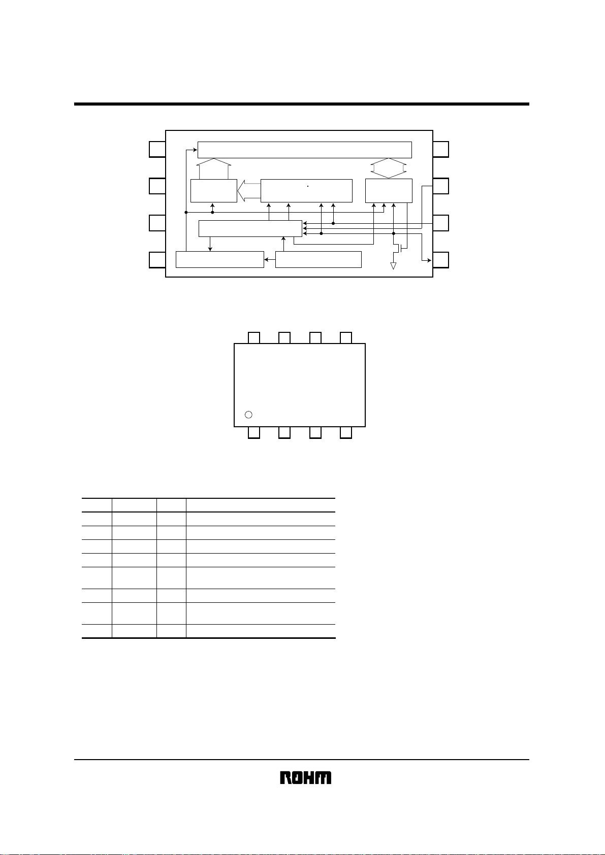
!!!!Block diagram
N.C.
1
1kbits EEPROM array
VCC8
N.C. 2
N.C. 3
GND 4
!!!!Pin assignment
7bits
Address
decoder
7bits
Slave word
address register
STOPSTART
Control logic
High voltage generator Vcc level detecter
SCL
VCC
VCLK
SDA
BR24C21
BR24C21F
BR24C21FJ
BR24C21FV
1234
N.C.
N.C.
N.C.
GND
8bits
Data
VCLK7
register
6 SCL
ACK
SDA5
5678
!!!!Pin descriptions
Pin name Function
1
2
3
4
5
6
7
8
∗ An open drain output requires a pull-up resistor.
N.C.
N.C.
N.C.
GND
SDA
SCL
VCLK
V
CC
I / OPin No.
−
No connection
−
No connection
−
No connection
Ground (0V)
−
Slave and word address,
I / O
serial data input, serial data output
I
Serial clock input for Bi-directional Mode
Clock input (Transmit-Only Mode)
I
Write enable (Bi-directional Mode)
−
Power supply
∗
Page 3
BR24C21 / BR24C21F / BR24C21FJ / BR24C21FV
Memory ICs
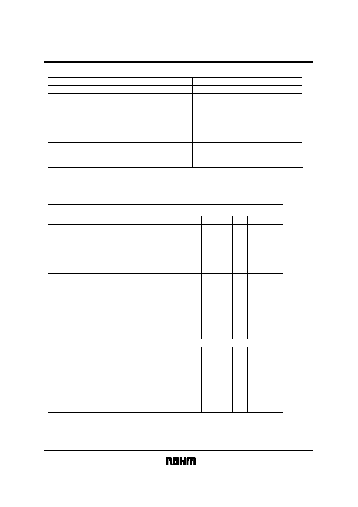
!!!!Electrical characteristics (Unless otherwise noted, Ta=−40∼85°C, VCC=2.5∼5.5V)
Parameter Symbol Min. Typ. Max. Unit Conditions
"HIGH" input volatge1
"LOW" input volatge1
"HIGH" input volatge2
"LOW" input volatge2
"LOW" input volatge3
"LOW" output volatge
Input leakage current I
Output leakage current I
Operating current I
Standby current
∗1 Transmit-Only Mode…After the power is on, the BR24C21, BR24C21F, BR24C21FJ and BR24C21FV are in Standby state without providing the clock on the VCLK pin.
Bi-directional Mode…The BR24C21, BR24C21F, BR24C21FJ and BR24C21FV are in Standby state after each command is porformed.
0.7V
IH1
V
V
IL1
V
IH2
V
IL2
V
IL3
V
OL
LI
LO
CC
I
SB
After the VCLK pin is provided the clock, the device is switched from Standby to Transmit-Only Mode, and the operating current runs.
CC
−−
−−
2.0
−−
−−
−−
−−
−1
−
−1 −
−
−
−
10 100
CC
0.3V
0.8 V
0.2V
CC
0.4 V
1 µA
1 µA
3.0 mA
µA
V
V
V
V
SCL, SDA
SCL, SDA
VCLK
VCLK,
V
CC≥
4.0V
VCLK,
V
CC<
4.0V
SDA, I
OL
=3.0mA
SCL,
VCLK,
VIN=0V~V
OUT
=0V~V
SCL
=400kHz
CC
SDA, V
V
CC
=5.5V, f
V
CC
=5.5V, SDA=SCL=VCC,
CC
=GND
∗1
VCLK
!!!!
Operating timing characteristics
(Unless otherwise noted, Ta=−40∼85°C, VCC=2.5∼5.5V)
Parameter Symbol
SCL frequency
Data clock "HIGH" time
Data clock "LOW" time t
SDA/SCL rise time t
SDA/SCL fall time t
Start condition hold time
Start condition setup time
Input data hold time
Input data setup time
Output data delay time (SCL) t
Stop condition setup time
Bus open time before start or transfer t
Noise erase valid time (SCL and SDA) t
<Transmit-Only Mode>
Output data delay time (VCLK) t
VCLK "HIGH" time
VCLK
"LOW" time t
VCLK setup time t
VCLK hold time t
Mode transition time t
Transmit-Only powerup time t
Noise erase valid time (VCLK) t
t
t
t
t
t
HD
SU
HD
SU
SU
SCL
f
t
HIGH
LOW
R
: STA
: STA
: DAT
: DAT
PD
: STO
BUF
t
WR
VPD
VHIGH
t
VLOW
VSU
VHD
VHZ
VPU
VI
Fast-mode
Vcc=2.5~5.5V
Min.
Typ.
Max.
−
−
400
0.6
−
1.3
−
−
F
−
0.6
0.6
0
100
−
0.6
1.3
−
I
−
−
0.6
1.3
0
0.6
−
0
−
0.3
−
0.3
−
−
−
−
−
0.9
−
−
−
−
10
−
0.1
1.0 −
−
−−
−
−
−
− 0.5
−
0.1
−
−
−
−
−
−
−
−
−
−
−
−
−
Standard-mode
Vcc=2.5~5.5V
Min.
Typ.
−
−
4.0
−
4.7
−
−
−
−
−
4.0
−
4.7
−
0
−
250
−
−
−
4.0
−
4.7
−
−
−
−
−
−
4.0
−−
4.7
−
0
−
4.0
−
−
− 1.0
0
−
−
−
Max.
100
−
−
1.0
0.3
−
−
−
−
3.5
−
−
10 msInternal write cycle time
0.1
2.0
−
−
−
−
0.1
Unit
kHz
µs
µs
µs
µs
µs
µs
ns
ns
µs
µs
µs
µs
µs
µs
µs
µs
µs
µs
µs
µs
Page 4
BR24C21 / BR24C21F / BR24C21FJ / BR24C21FV
Memory ICs
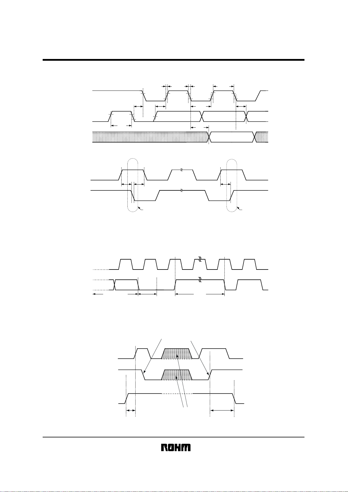
!!!!Timing charts
SYNCHRONOUS DATA TIMING
t
HIGH
SCL
SDA
(IN)
SDA
(OUT)
t
R
t
HD :
STA t
t
BUF
tSU : DAT tHD : DAT
t
F
LOW
t
PD
SCL
SDA
START BIT STOP BIT
Fig.7
•SDA data is latched into the chip at the rising edge of the SCL clock.
•Output data toggles at the falling edge of the SCL clock.
WRITE CYCLE TIMING
SCL
SDA
WRITE DATA
(n)
ACKD0
Fig.8
WRITE ENABLE TIMING
START BIT
STOP BIT
tSU : STOtHD : STAtSU : STA
t
WR
START CONDITIONSTOP CONDITION
SCL
SDA
VCLK
t
VSU
WRITE COMMAND
Fig.9
t
VHD
Page 5

BR24C21 / BR24C21F / BR24C21FJ / BR24C21FV
Memory ICs
!!!!Circuit operation
The BR24C21, BR24C21F, BR24C21FJ and BR24C21FV operate in two modes, Transmit-Only Mode and Bi-directional
Mode. The devices operate in Transmit-Only Mode when they will power up. In this mode, the devices transmit data on
the SDA pin with the VCLK clock. This mode is continued by providing a valid high to low transition on the SCL pin.
The devices can be switched into Bi-directional Mode by providing a valid high to low transition on the SCL pin. They
begin to count the VCLK clock at once. If the VCLK counter reaches 128 clock without the command for Bi-directional
Mode, the device revert to Transmit-Only Mode. (Recovery function) If the devices are received the command for Bidirectional Mode and respond with an Acknowledge before the VCLK counter reaches 128 clock, it is impossible to revert
to Transmit-Only Mode. (The way to switch Bi-directional Mode to Transmit-Only Mode is that the power down again.)
* When the power is on, the SCL pin set to V
(High level).
CC
(1) Transmit-Only Mode
•After the power is on, the BR24C21, BR24C21F, BR24C21FJ and BR24C21FV are in Transmit-Only Mode. In this
mode, the data can be output by providing the clock on the VCLK pin.
(High level).
•When the power is on, the SCL pin set to V
CC
•The state of SDA is high-impedance during input of the first 9 clocks, and a data is output starting with the 10th rising
clock edge on VCLK. After the power is on, the output data is as follow
00h address data → 01h address data → 02h address data → …
The address is incremented by one with every 9 clock of VCLK. All address is output in this mode. When the counter
reaches the last address, the next output data is 00h address data.
•In the mode, the NULL bit (High data) is output between the address data and the next address data.
•The read operation in Transmit-Only Mode can be started after the power stabilized.
CC
V
SCL
1910
VCLK
t
VPU
SDA
VCLK
SDA
Fig.10 TRANSMIT-ONLY MODE
t
VHIGHtVLOW
t
VPD
D1 D0 D7 D6
ADDRESS n
DATA
NULL BIT
DATA=1
Fig.11 NULL BIT
D3D4D5D6D7
00h ADDRESS DATA
ADDRESS n+1
DATA
Page 6

BR24C21 / BR24C21F / BR24C21FJ / BR24C21FV
Memory ICs
(2) Bi-directional Mode
1) Bi-directional Mode and Recovery function
•The BR24C21, BR24C21F, BR24C21FJ and BR24C21FV can be switched from Transmit-Only Mode to
Bi-directional Mode by providing a valid high to low transition on the SCL pin, and the state of SDA is high-impedance.
•After a valid high to low transition on the SCL pin, the BR24C21, BR24C21F, BR24C21FJ and BR24C21FV begin to
count the VCLK clock. If the VCLK counter reaches 128 clock without the command for Bi-directional Mode, the
device revert to Transmit-Only Mode. (Recovery function) The VCLK counter is reset by providing a valid high to low
transition on the SCL pin. After reversion to Transmit-Only Mode, the devices begin to output a data with the 129th
rising clock edge on VCLK. The output data is 00h address data at the time.
•If the BR24C21, BR24C21F, BR24C21FJ and BR24C21FV are switched from Transmit-Only Mode and received
the command for Bi-directional Mode and responds with an Acknowledge, it is impossible to revert to Transmit-Only
Mode. (The only way to revert to Transmit-Only Mode is that the power down again.) Unless the input device code is
“1010”, the device responds no Acknowledge. If the VCLK counter reaches 128 clock afterward, it is possible to revert
to Transmit-Only Mode for Recovery function. If the master generates a stop condition during the slave address input,
it is possible to revert to Transmit-Only Mode.
•When the devices are switched from Transmit-Only Mode to Bi-directional Mode, the period of t
need to be held.
VHZ
MODE
VCLK
SCL
SDA
MODE
VCLK
SCL
SDA
Transmit-only
Transmit-Only
Bi-directional
Transition Mode with possibility to return to Transmit-Only Mode
VHZ
t
Bi-directional
Transition Mode with possibility to return to Transmit-Only Mode
2n
1
VHZ
t
n<128
Fig.12 RECOVERY MODE
1291281273214
Transmit-Only
ADDRESS 00h
R/W ACKS1010∗∗∗
D4D5D6D7
Bi-directional
parmanently
Fig.13 MODE CHANGE
Page 7

BR24C21 / BR24C21F / BR24C21FJ / BR24C21FV
Memory ICs
2) Bi-directional Mode
START CONDITION
•All commands are proceeded by the start condition, which is a HIGH to LOW transition of SDA when SCL is HIGH.
•The BR24C21, BR24C21F, BR24C21FJ and BR24C21FV continuously monitors the SDA and SCL lines for the start
condition and will not respond to any command until this condition has been met.
STOP CONDITION
•All communications must be terminated by a stop condition, which is a LOW to HIGH transition of SDA when SCL is
HIGH.
•The stop condition initiates internal write cycle to write the data into memory array after write sequence.
•The stop condition is also used to place the device into the standby power mode after read sequence.
•A stop condition can only be issued after the transmitting device has released the bus.
DEVICE ADDRESSING
•Following a START condition, the master output the device address of the slave to be accessed. The most significant
four bits of the slave address are the “device type indentifier”, For the BR24C21, BR24C21F, BR24C21FJ and
BR24C21FV this is fixed as “1010”.
•The next three bits of the slave address are don’t care.
•The last bit of the stream determines the operation to be performed. When set to “1”, a read operation is selected ;
when set to “0”, a write operation is selected.
R / W set to “0” ··· WRITE
(This bit also sets to “0” for random read operation)
R / W set to “1” ··· READ
∗∗∗1010 R / W
∗ Don't care
WRITE PROTECT FUNCTION
•WRITE ENABLE (VCLK)
When using the BR24C21, BR24C21F, BR24C21FJ and BR24C21FV in the Bi-directional Mode, the VCLK pin can
be used as a write enable pin. Setting VCLK high allows normal write operations, while setting VCLK low prevents
writing to any location in the array. Changing VCLK from high to low during the self-timed program operation will not
halt programming of the device. Setting VCLK low allow the word address setting in random read.
Page 8

BR24C21 / BR24C21F / BR24C21FJ / BR24C21FV
Memory ICs
ACKNOWLEDGE
•Acknowledge is a software convention used to indicate successful data transfers. The master or the slave will release
the bus after transmitting eight bits. During the ninth clock cycle, the receiver will pull the SDA line LOW to
acknowledge that the eight bits of data has been received.
•The BR24C21, BR24C21F, BR24C21FJ and BR24C21FV will respond with an Acknowledge after recognition of a
START condition and its slave address. If both the device and a write operation have been selected, the BR24C21,
BR24C21F, BR24C21FJ and BR24C21FV will respond with an Acknowledge, after the receipt of each subsequent
8-bit word.
•In the READ mode, the BR24C21, BR24C21F, BR24C21FJ and BR24C21FV will transmit eight bits of data, release
the SDA line, and monitor the line for an Acknowledge.
•If an Acknowledge is detected, and no STOP condition is generated by the master, the BR24C21, BR24C21F,
BR24C21FJ, BR24C21FV will continue to transmit the data.
•If an Acknowledge is not detected, the BR24C21, BR24C21F, BR24C21FJ and BR24C21FV will terminate further
data transmissions and await a STOP condition before returning to the standby mode.
START CONDITION
(START BIT)
SCL
(From µ−COM)
SDA
(µ−COM
OUTPUT DATA)
SDA
(IC OUTPUT DATA)
3) Bi-directional Mode Command
BYTE WRITE
S
T
A
R
T
SDA
LINE
10 01
189
Fig.14 ACKNOWLEDGE RESPONSE FROM RECEIVER
W
R
SLAVE
ADDRESS
I
T
E
R
A
/
C
W
K
WA
∗∗∗∗
WORD
ADDRESS
6
WA
Acknowledge Signal
(ACK Signal)
S
D0
T
O
P
A
C
K
DATA
D7
0
A
C
K
VCLK
∗Don't care
Fig.15 BYTE WRITE CYCLE TIMING
•When the master generates a STOP condition, the BR24C21, BR24C21F, BR24C21FJ and BR24C21FV begin the
internal write cycle to the nonvolatile array.
Page 9

BR24C21 / BR24C21F / BR24C21FJ / BR24C21FV
Memory ICs
PAGE W RITE
S
T
A
R
T
SLAVE
ADDRESS
W
R
I
T
E
WORD
ADDRESS(n)
DATA(n)
DATA(n+7)
S
T
O
P
SDA
LINE
VCLK
10 01
∗∗∗
WA
∗
6
A
R
C
/
K
W
Fig.16 PAGE WRITE CYCLE TIMING
WA
D7
0
A
C
K
D0
A
C
K
D0
A
C
K
∗Don't care
•If the master transmits the next data instead of generating a stop condition in byte write cycle, the BR24C21,
BR24C21F, BR24C21FJ and BR24C21FV transfer from byte write cycle to page write cycle. After the receipt of each
word, the three lower order address pointer bits are internally incremented by one. The high order five bits of the word
address remains constant.
If the master transmits more than eight words, prior to generating the STOP condition, the address counter will “roll
over”, and the previous transmitted data will be overwritten.
CURRENT READ
SDA
LINE
S
T
A
R
T
11
00
SLAVE
ADDRESS
∗∗∗
R
E
A
D
D7 D0
DATA
S
T
O
P
R
A
/
C
W
K
Fig.17 CURRENT READ CYCLE TIMING
A
C
K
•The BR24C21, BR24C21F, BR24C21FJ and BR24C21FV contain an internal address counter which maintains the
address of the last word accessed, incremented by one. If the last accessed address is address n in a read operation,
the next read operation will access data from address n+1 and increment the current address counter. If the last
accessed address is address n in a write operation, the next read operation will access data from address n. If the
master does not transfer the acknowledge but does generate a stop condition, the current address read operation
only provides a single byte of data. At this point, the device discontinues transmission.
Page 10

BR24C21 / BR24C21F / BR24C21FJ / BR24C21FV
Memory ICs
RANDOM READ
S
T
A
R
T
SLAVE
ADDRESS
W
R
I
T
E
WORD
ADDRESS(n)
S
T
A
R
T
SLAVE
ADDRESS
R
E
A
D
DATA(n)
S
T
O
P
SDA
LINE
1100∗∗∗
WA
∗
6
R
A
/
C
W
K
Fig.18 RANDOM READ CYCLE TIMING
WA
0
A
C
K
1100
∗∗∗
D7 D0
R
A
/
C
W
K
A
C
K
•Random read operation allows the master to access any memory location. This operation involves a two-step
process. First, the master issues a write command which includes the start condition and the slave address field (with
R / W set to “0”) followed by the address of the word to be read. This procedure sets the internal address counter of
the BR24C21, BR24C21F, BR24C21FJ and BR24C21FV to the desired address. After the word address
acknowledge is received by the master, the master immediately reissues a start condition followed by the slave
address field with R / W the set to “1”. The device will respond with an acknowledge and then transmit the 8-data bits
stored at the addressed location. If the master does not acknowledge the transmission but does generate the stop
condition, at this point BR24C21, BR24C21F, BR24C21FJ and BR24C21FV discontinue transmission.
SEQUENTIAL READ
SDA
LINE
S
T
A
R
ADDRESS
T
1100
SLAVE
∗∗∗
R
E
A
D
DATA(n)
D7 D7D0 D0
DATA(n+x)
S
T
O
P
A
R
C
/
K
W
Fig.19 SEQUENTIAL READ CYCLE TIMING
A
C
K
(Current Read)
A
C
K
A
C
K
•During the sequential read operation, the internal address counter of the BR24C21, BR24C21F, BR24C21FJ and
BR24C21FV automatically increments with each acknowledge received ensuring the data from address n will be
followed with the data from n+1. For read operations, all bits of the address counter are incremented allowing the
entire array to be read during a single operation. When the counter reaches the top of the array, it will “roll over” to the
bottom of the array and continue to transmit the data.
•The sequential read operation can be performed with both current read and random read.
Page 11

BR24C21 / BR24C21F / BR24C21FJ / BR24C21FV
Memory ICs
!!!!
External dimension
3.2 ± 0.2 3.4 ± 0.3
6.0 ± 0.3
1.375 ± 0.1
(Units : mm)
9.3 ± 0.3
85
14
0.51Min.
2.54
4.9 ± 0.2
85
76
3.9 ± 0.2
4123
0.175
1.27
0.42 ± 0.1
0.5 ± 0.1
DIP8
0.1
6.5 ± 0.3
0.45Min.
7.62
0°~15°
0.2 ± 0.1
0.3 ± 0.1
6.2 ± 0.3
1.5 ± 0.1
6.4 ± 0.3
(0.52)
85
4.4 ± 0.2
1.27
0.11
3.0 ± 0.2
4.4 ± 0.2
1
0.65
5.0 ± 0.2
548
0.22 ± 0.1
41
0.4 ± 0.1
0.1
0.3Min.
SOP8
1.15 ± 0.1
0.15 ± 0.1
0.15
0.15 ± 0.1
0.3Min.
0.1
SOP-J8
SSOP-B8
 Loading...