Page 1

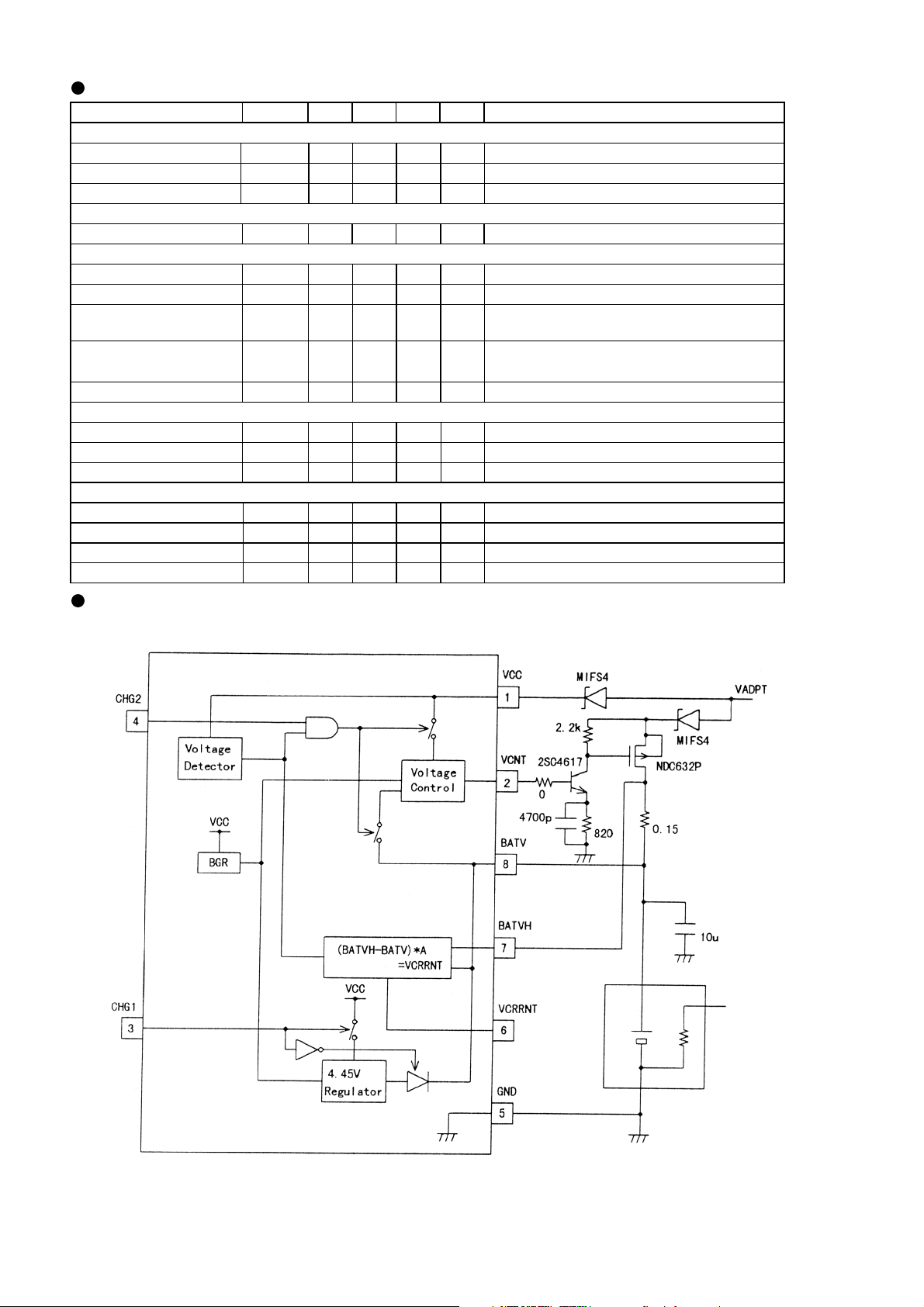
Charging control driver IC for
Portable telephone
BH3890FV
99W063A
Description
The BH3890FV is a charging IC developed for a
lithium ion battery (1 cell). Back-up charging circuit
and charging current monitor circuit are included.
This IC is directed by a micro computer controller.
Features
1) Built-in charging driver circuit
2) Built-in charging current monitor circuit
3) Built-in back-up charging circuit
4) Small package SSOP-B8
Applications
Portable telephone, PHS, equipment involving lithium ion battery
Absolute Maximum Ratings(Ta=25˚C)
SymbolParameter
Maximum supply voltage
Power dissipation
Operating temperature range
Storage temperature range
* Derating : 3.0mW/˚C for operation above Ta=25˚C.
VCCMAX
Pd
Topr
Tstg
Limits
–0.3 +7.0
~
*
300
+70
~
–20
+125
~
–55
Dimension (Units : mm)
SSOP-B8
Unit
V
mW
˚C
˚C
Recommended Operating Conditions (Ta=25˚C)
Parameter Symbol UnitMin. Typ. Max.
Power supply voltage V
CC
—
V5 6
November, 1999
Page 2

Electrical Characteristics
Parameter
<VCC circuit current>
Circuit current 1
Circuit current 2
Circuit current 3
<BATV circuit current> (Current influx into BATV terminal )
Circuit current 4
<CURRENT>
Output voltage 1
Output voltage 2
Coefficient of output
voltage inclination
Ripple rejection rate
Starting up voltage
<REG> (CHG1=ON, CHG2=OFF)
Output voltage
Ripple rejection rate
Maximum output current
<CHARGE> (CHG1=OFF, CHG2=ON)
Control voltage
Ripple rejection rate
Load regulation
Input voltage stability
(Unless otherwise noted, Ta=25˚C, Vcc= 5.5V, BPF=20 ~ 20kHz)
—
—
—
—
2.37
0.44
12.7
—
4.35
30
10
4.15
30
—
—
Typ.
530
800
1.0
1.7
1.4
2.1
0
5
2.57
2.77
0.54
0.64
13.5
14.3
40 — dB
—
3.5
4.45
4.55
40
—
15
20
4.20
4.25
40
—
5
30
5
30
Symbol
IQ1
IQ2
IQ3
IQ4
VOC1
VOC2
LINC
RRC 30
VCCST
VOR
RRR
IORMAX
VOB
RRB
∆ VOB1
∆ VOB2
UnitMin. Max.
µA
CHG1=OFF, CHG2=OFF
mA
CHG1=ON, REG=No load
mA
CHG2=ON, CHARGE section=No load
µA
CHG1=OFF, CHG2=OFF, Vcc=0V BATV=4.0V
V
VBATVH–VBATV=150mV
V
VBATVH–VBATV=0V
—
LINC=(VOC1–VOC2) / 0.15
VR=–20dBV, fR=100Hz, VBATVH=4.215V,
VBATV=4.2V
V
VCC (VOC2≥ 0.4V)
IO=5mA
V
dB
VR=–30dBV, fR=100Hz, IO=5mA
mA
VOR≤ 4.0V
V
IO=100mA
dB
VR=–20dBV, fR=100Hz, IO=100mA
mV
IO=1~800mA
mV
VCC=5.0~6.0V, IO=100mA
Conditions
Application circuit
 Loading...