

Page 1
5-channel switching regulator controller
BD9731KV
01W038A
Description
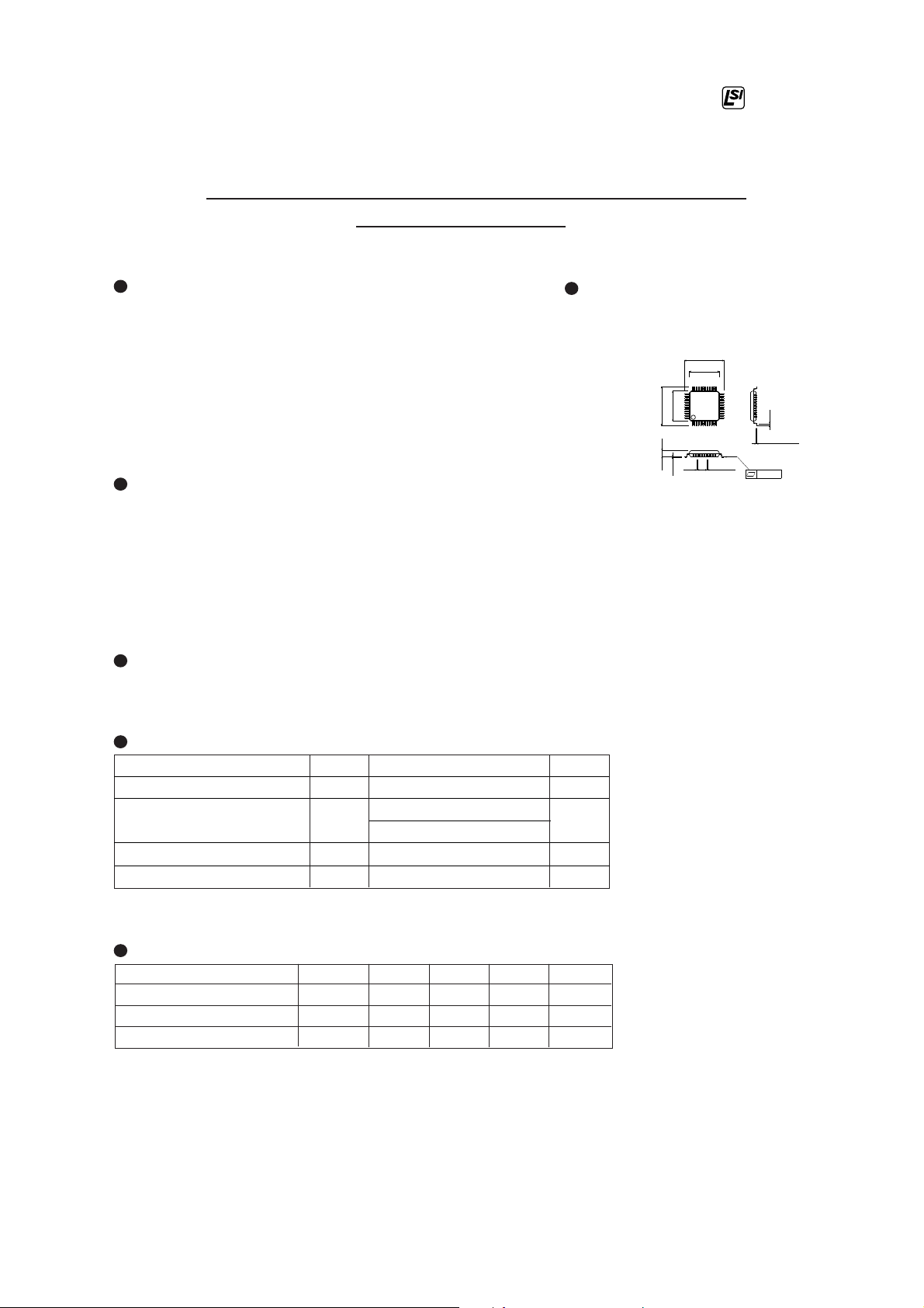
Dimension (Units : mm)
BD9731KV is a PWM switching regulator controller IC.
The 5-channel (4 channel for step-up, and 1 channel for
step-down) switching regulator controllers are integrated
into a VQFP48 package. This IC can operate both Bipolar
and MOS transistor. Triangle wave oscillator, reference
voltage, PWM comparator, CMOS type driver, and short
protection circuit are integrated.
Features
1) Can operate both external transistors of Bipolar and MOS.
(Base current can be set by resistance.)
2) Built-in output shutdown circuit (Timer latch) when overloaded.
3) Channel 1, and 5 can externally set the reference voltage.
4) Channel 1, 4, and 5 can control independently ON/OFF.
5) All channels have dead time control.
Applications
Digital still camera, Portable DVD player, W-CDMA, PDA, Digital movie camera
37
0.2
±
7.0
9.0±0.3
48
0. 1
±
0.5
1.425
0. 10
VQFP48
9.0±0.3
7.0±0.2
1
2536
12
0.2±0. 1
24
13
0.4
0. 15±0.1
0. 10
Absolute Maximum Ratings (Ta=25˚C)
–20
–55
Limits
~
400
900
~
~
+12–0.3
∗1
∗2
+85
+125
Parameter Symbol
Maximum applied voltage
Power dissipation
Operating temperature range
Storage temperature range
∗Derating : 4.0mW/˚C for operation above Ta=25˚C (Only IC unit)
∗PCB (70mmx70mm, t=1.6mm) glass epoxy mounting. Derating : 9.0mW/˚C for operation above Ta=25˚C
Vmax
Pd
Topr
Tstg
Recommended Operating Conditions (Ta=25˚C)
Parameter Min. Max. UnitTyp.Symbol
Power supply voltage
Oscillating frequency
Output current
VCC
fosc
IOUT
100 700 kHz
—2.8 11
—
—— 30
Unit
V
mW
˚C
˚C
V
mA
May, 2001
Page 2
Electrical characteristics (Unless otherwise noted; Ta=25˚C, Vcc=6V, fosc=0.20MHz, STB1~5=3V)
Symbol Min. Max. Unit ConditionsTyp.Parameter
Circuit current at stand-by
Circuit current at operating
<Reference voltage>
Output voltage
<Internal regulator>
Output voltage REGA
<Shutdown at overloaded>
CH1~5 threshold voltage
<Protection circuit>
SCP pin detection circuit
Triangle wave oscillator
Oscillating frequency
<Output>
Output voltage 'H' at operating
Output voltage 'L' at operating
Maximum output source current
Maximum output sink current
<STB1~5>
STB pin
control voltage
Operating
Non-operating
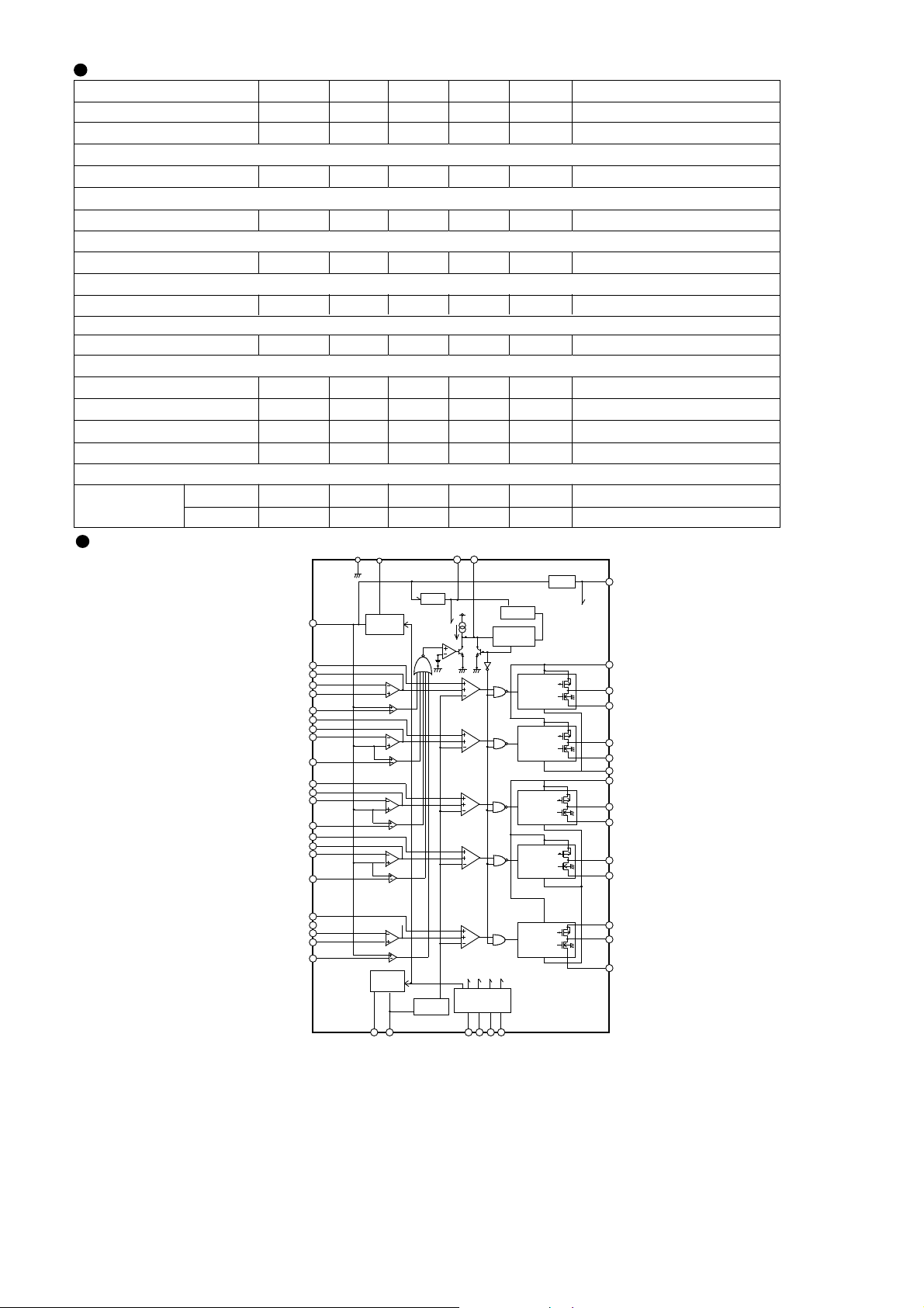
Block Diagram
Ist —
Icc
Vref
VREGA
Vsc1~5
Vtsc
fosc1 0.179
VSATH
Vcc–0.3
VSATL
IOSOURCE
Iosink
VSTBL
VSTBH
34
VREF
43
DTC1
40
FB1
41
INV1
42
NON1
39
SCP1
38
DTC2
36
FB2
35
INV2
37
SCP2
26
DTC3
24
FB3
23
INV3
25
SCP3
19
DTC4
21
FB4
22
INV4
20
SCP4
—
1.485
2.4
1.425
0.90
—
—
—
2.0
–0.3
30.GND
ERRAMP1
ERRAMP2
ERRAMP3
ERRAMP4
Vcc–0.1
32.VCC
VOLTAGE
REFERENCE
SCPcomp1
SCPcomp2
SCPcomp3
SCPcomp4
—
4.5
1.5
2.5
1.5
1.0
0.20
0.1
—
—
—
—
To Control
REG A
Block
1.515
1.575
1.10
0.221
–30
VREGA
PWM
PWM
PWM
PWM
10
9.5
2.6
—
0.3
30
—
0.3
2933
SCP
U.V.L.O
TIMER LATCH
S
Q
Pch DRIVER
Pch DRIVER
Pch DRIVER
Pch DRIVER
µA
mA
V
V
V
V
MHz
V
V
mA
mA
V
V
R
STB1~5=0V
Iref=–1mA
Ireg=–1mA
VSCP1~5=2V~1V
VSCP=0V~1.5V
RT=24kΩ, CT=220pF
Io=10mA
Io=–10mA
REG D
To-Divers
31
44
10
3
2
1
4
5
8
7
6
9
VREGD
PVCC1
OUT1
RBIAS1
OUT2
RBIAS2
PGND1
PVCC2
OUT3
RBIAS3
OUT4
RBIAS4
DTC5
INV5
NON5
SCP5
14
16
FB5
17
18
15
ERRAMP5
SCPcomp5
28 48 47 46 45
27
RT
CT
PWM
Nch DRIVER
BD9731KV
STB1
STB5
STB4
STB23
13
12
11
RBIAS5
OUT5
PGND2
 Loading...