Page 1

Programmable negative supply IC
BD6112FVM
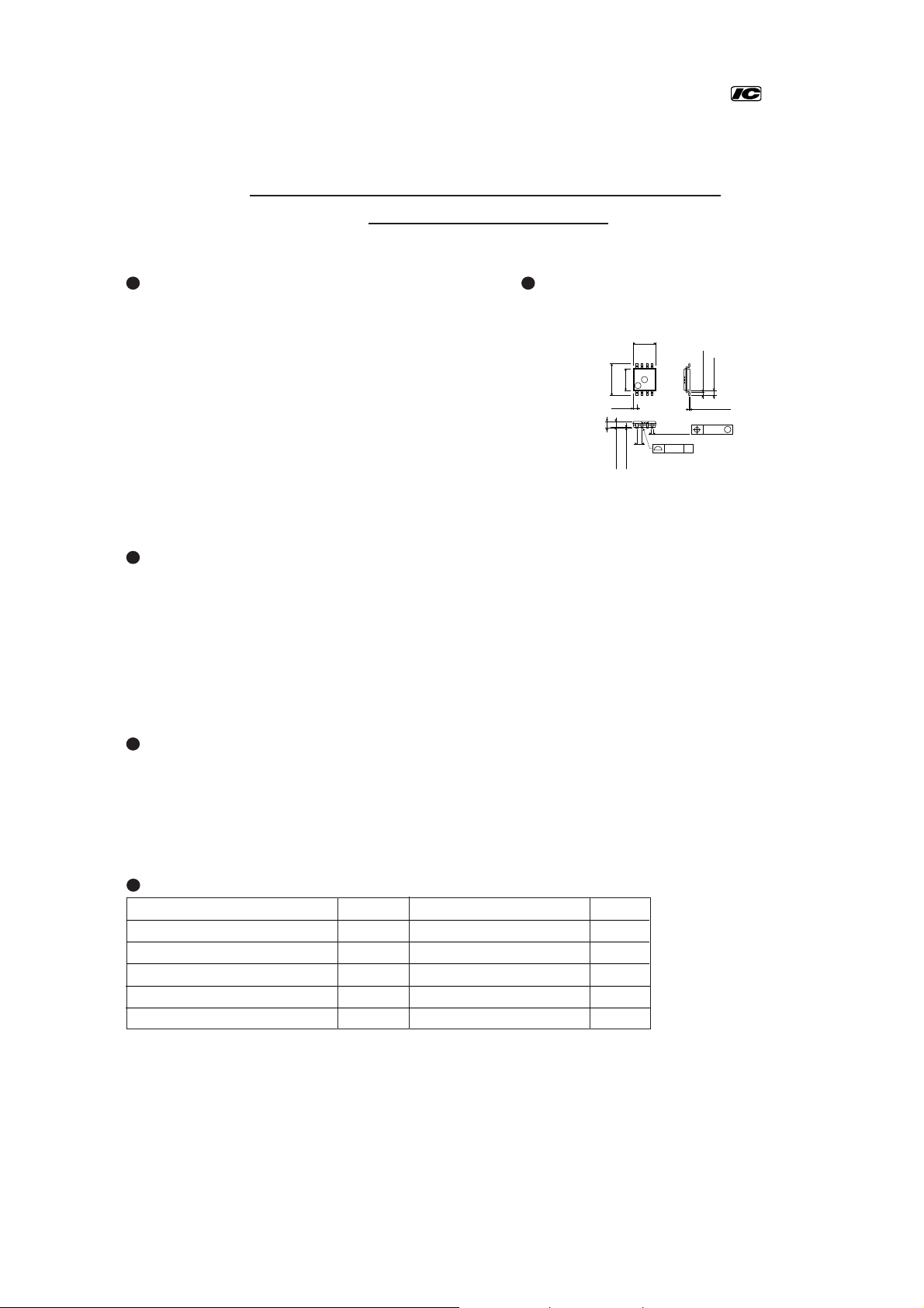
Description Dimension (Units : mm)
BD6112FVM is a charge-pump negative supply IC
with a built-in regulator. The charge-pump block
inverts the positive supply voltage in the VBAT pin
into a negative voltage, which generates from the
NEGOUT pin. The regulator block stabilizes
this negative voltage with low-noise that produces
from the OUT pin. Output voltage values of this
regulator can be controlled by voltage value inputted
to the VIN pin and determined by OUT=—1.6 x VIN.
0.9Max.
4.0±0.2
0.475
2.8±0.1
0.75±0.05
2.9±0.1
58 7 6
41 2 3
0.65
0.08±0.05
MSOP8
0.22
+0.05
-
0.04
0.08 S
0.29±0.15
0.145
0.08
00W148A
0.6±0.2
+0.05
-
0.03
M
Features
1) Built-in high efficiency, inverting charge-pump
2) Built-in negative voltage regulator
(low noise, output voltage variable)
3) Built-in standby SW (pull down resistance 1MΩ)
4) Ultra small MSOP8 package
Applications
Small terminal devics such as cellular phones, PHS, and PDA etc.
Other equipments driven by battery required for negative voltage.
Absolute Maximum Ratings (Ta=25˚C)
–0.3
–0.3
Limits
~
~
350
~
~
+6.0
+6.0
*
+85–30
+125–55
Parameter Symbol
Maximum applied supply voltage
Maximum applied input voltage
Power dissipation
Operating temperature range
Storage temperature range
VBAT
VIN
Pd
Topr
Tstg
*Derating : 3.5mW/˚C for operation above Ta=25˚C
Unit
V
V
mW
˚C
˚C
February, 2001
Page 2

Recommended Operating Conditions (Ta=25˚C)
Parameter Min. Max. UnitTyp.Symbol
Power supply voltage
VBAT
V5.53.62.5
Electrical characteristics (Unless otherwise noted; Ta=25˚C, VBAT=3.6V, STBY=3.6V)
Symbol Min. Max. Unit ConditionsTyp.Parameter
Circuit current
Stand-by current
<Regulator block>
Output voltage 1
Output voltage 2
Output ripple voltage
Maximum output current
Load regulation
Line regulation
VIN pin inflow current
<Charge-pump block>
Oscillation frequency
Voltage conversion efficiency
Stand-by pin pull down resistance
Stand-by pin
control voltage
Operating
Non-operating
IQ1 –
IQ2
Vo
Vo2
Vo x 0.95
VRR
IOMAX
∆VOL
∆VOI
IIN
fosc
VCE
RSTBY
VIH
VIL
–
–2.1
–
10
–
–
–
–
–
0.6
2.0
–0.3
0.5
–
–2.0
Vo
–70
–
2
10
0
120
97
1.0
–
–
3
5
–1.9
Vo x 1.05
–60
–
40
40
2
–
–
1.6
–
0.3
mA
µA
V
V
dBV
mA
mV
mV
µA
kHz
%
MΩ
V
V
No load, VIN=1.25V
No load, VIN=0V, STBY=0V
VIN=1.25V, IOUT=5mA
VIN=0.5~1.8V, Vo=–1.6 x VIN,IOUT=5mA
VIN=1.25V, IOUT=5mA
VIN=1.25V, VOUT≤Vo+0.1V
VIN=1.25V, Io=0~5mA
VBAT=3.0~6.0V, Io=5mA
VIN=1.25V
No load, NEGOUT monitor
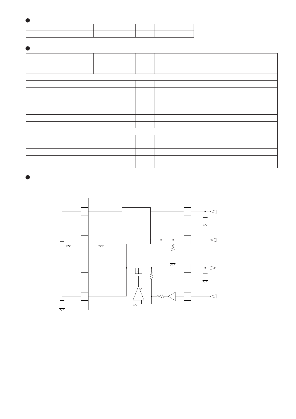
Application Circuit
+
C1
1µ
NEGOUT
C2
+
1
µ
GND
C+
C-
1
CHARGE
VBAT
8
1µ
+
C4
PUMP
2
1M
3
1.6M
4
+ -
+
1M
BD6112FVM
STBY
7
OUT
6
+
1µ
C3
VIN
5
 Loading...