

Page 1
BD48XXG/FVE
Voltage detectors
BD49XXG/FVE
CMOS RESET IC
BD48XXG/FVE
BD49XXG/FVE
Rohm's BD48XXG/FVE and BD49XXG/FVE are series of high-accuracy, low-power VOLTAGE DETECTOR ICs
with a CMOS process. For flexible choice according to the application, BD48XXG/FVE series with N channel
open drain output and BD49XXG/FVE series with CMOS output are available in 38 voltage types from 2.3 V to
6.0 V in steps of 0.1 V in different packages, totaling 152 models.
Applications
Every kind of appliances with microcontroller and logic circuit
Features
1) Detection voltage: 0.1V step line-up 2.3 to 6.0V (Typ.)
2) High-accuracy detection voltage: ±1.5% guaranteed (Ability ±1%)
3) Ultra low current consumption: 0.8 A typ. (Output is High.)
4) Nch open drain output (BD48XXG/FVE series),
CMOS output (BD49XXG/FVE series)
5) Small package VSOF5(EMP5) : BD48XXFVE/BD49XXFVE
SSOP5(SMP5C2) : BD48XXG/BD49XXG
Selection guide
For BD4XXXX series, detection voltage, output circuit types (Refer to the block diagram at P3), and package
(Refer to the dimension at P14) can be selected for your own application.
Part number of devices for each specification is shown below.
Part No. : B D 4 X X X X
1 2
Part No. Specification Contents
1
2
3
Output circuit types
Detection voltage
Package
8 : Open drain output
9 : CMOS output
Ex. : VS : described in each 0.1V step
for 2.3V to 6.0V range (29 means 2.9V)
G : SSOP5 (SMP5C2)
FVE : VSOF5 (EMP5)
3
Rev.A
1/15
Page 2
Voltage detectors
Line-up
BD48XXG/FVE
BD49XXG/FVE
Detection
voltage
VS
Nch Open drain output
( BD48XXG/FVE )
CMOS output
( BD49XXG/FVE )
Detection voltage VS ( V ) Ta=25°C
Min. Typ. Max.
6.0V BD4860G/FVE BD4960G/FVE 5.910 6.000 6.090
5.9V
5.8V
5.7V
5.6V
5.5V
5.4V
5.3V
5.2V
5.1V
5.0V
4.9V
4.8V
4.7V
4.6V
4.5V
4.4V
4.3V
4.2V
4.1V
4.0V
3.9V
3.8V
3.7V
3.6V
3.5V
3.4V
3.3V
3.2V
3.1V
3.0V
2.9V
2.8V
2.7V
2.6V
2.5V
2.4V
2.3V
BD4859G/FVE
BD4858G/FVE
BD4857G/FVE
BD4856G/FVE
BD4855G/FVE
BD4854G/FVE
BD4853G/FVE
BD4852G/FVE
BD4851G/FVE
BD4850G/FVE
BD4849G/FVE
BD4848G/FVE
BD4847G/FVE
BD4846G/FVE
BD4845G/FVE
BD4844G/FVE
BD4843G/FVE
BD4842G/FVE
BD4841G/FVE
BD4840G/FVE
BD4839G/FVE
BD4838G/FVE
BD4837G/FVE
BD4836G/FVE
BD4835G/FVE
BD4834G/FVE
BD4833G/FVE
BD4832G/FVE
BD4831G/FVE
BD4830G/FVE
BD4829G/FVE
BD4828G/FVE
BD4827G/FVE
BD4826G/FVE
BD4825G/FVE
BD4824G/FVE
BD4823G/FVE
BD4959G/FVE
BD4958G/FVE
BD4957G/FVE
BD4956G/FVE
BD4955G/FVE
BD4954G/FVE
BD4953G/FVE
BD4952G/FVE
BD4951G/FVE
BD4950G/FVE
BD4949G/FVE
BD4948G/FVE
BD4947G/FVE
BD4946G/FVE
BD4945G/FVE
BD4944G/FVE
BD4943G/FVE
BD4942G/FVE
BD4941G/FVE
BD4940G/FVE
BD4939G/FVE
BD4938G/FVE
BD4937G/FVE
BD4936G/FVE
BD4935G/FVE
BD4934G/FVE
BD4933G/FVE
BD4932G/FVE
BD4931G/FVE
BD4930G/FVE
BD4929G/FVE
BD4928G/FVE
BD4927G/FVE
BD4926G/FVE
BD4925G/FVE
BD4924G/FVE
BD4923G/FVE
5.812
5.713
5.615
5.516
5.418
5.319
5.221
5.122
5.024
4.925
4.827
4.728
4.630
4.531
4.433
4.334
4.236
4.137
4.039
3.940
3.842
3.743
3.645
3.546
3.448
3.349
3.251
3.152
3.054
2.955
2.857
2.758
2.660
2.561
2.463
2.364
2.266
5.900
5.800
5.700
5.600
5.500
5.400
5.300
5.200
5.100
5.000
4.900
4.800
4.700
4.600
4.500
4.400
4.300
4.200
4.100
4.000
3.900
3.800
3.700
3.600
3.500
3.400
3.300
3.200
3.100
3.000
2.900
2.800
2.700
2.600
2.500
2.400
2.300
5.989
5.887
5.786
5.684
5.583
5.481
5.380
5.278
5.177
5.075
4.974
4.872
4.771
4.669
4.568
4.466
4.365
4.263
4.162
4.060
3.959
3.857
3.756
3.654
3.553
3.451
3.350
3.248
3.147
3.045
2.944
2.842
2.741
2.639
2.538
2.436
2.335
Hysteresis
voltage
( V,Typ. )
VS X 0.05
SSOP5
SSOP5
SSOP5
SSOP5
SSOP5
SSOP5
SSOP5
SSOP5
SSOP5
SSOP5
SSOP5
SSOP5
SSOP5
SSOP5
SSOP5
SSOP5
SSOP5
SSOP5
SSOP5
SSOP5
SSOP5
SSOP5
SSOP5
SSOP5
SSOP5
SSOP5
SSOP5
SSOP5
SSOP5
SSOP5
SSOP5
SSOP5
SSOP5
SSOP5
SSOP5
SSOP5
SSOP5
SSOP5
Package
(SMP5C2)
(SMP5C2)
(SMP5C2)
(SMP5C2)
(SMP5C2)
(SMP5C2)
(SMP5C2)
(SMP5C2)
(SMP5C2)
(SMP5C2)
(SMP5C2)
(SMP5C2)
(SMP5C2)
(SMP5C2)
(SMP5C2)
(SMP5C2)
(SMP5C2)
(SMP5C2)
(SMP5C2)
(SMP5C2)
(SMP5C2)
(SMP5C2)
(SMP5C2)
(SMP5C2)
(SMP5C2)
(SMP5C2)
(SMP5C2)
(SMP5C2)
(SMP5C2)
(SMP5C2)
(SMP5C2)
(SMP5C2)
(SMP5C2)
(SMP5C2)
(SMP5C2)
(SMP5C2)
(SMP5C2)
(SMP5C2)
/ VSOF5
/ VSOF5
/ VSOF5
/ VSOF5
/ VSOF5
/ VSOF5
/ VSOF5
/ VSOF5
/ VSOF5
/ VSOF5
/ VSOF5
/ VSOF5
/ VSOF5
/ VSOF5
/ VSOF5
/ VSOF5
/ VSOF5
/ VSOF5
/ VSOF5
/ VSOF5
/ VSOF5
/ VSOF5
/ VSOF5
/ VSOF5
/ VSOF5
/ VSOF5
/ VSOF5
/ VSOF5
/ VSOF5
/ VSOF5
/ VSOF5
/ VSOF5
/ VSOF5
/ VSOF5
/ VSOF5
/ VSOF5
/ VSOF5
/ VSOF5
(EMP5)
(EMP5)
(EMP5)
(EMP5)
(EMP5)
(EMP5)
(EMP5)
(EMP5)
(EMP5)
(EMP5)
(EMP5)
(EMP5)
(EMP5)
(EMP5)
(EMP5)
(EMP5)
(EMP5)
(EMP5)
(EMP5)
(EMP5)
(EMP5)
(EMP5)
(EMP5)
(EMP5)
(EMP5)
(EMP5)
(EMP5)
(EMP5)
(EMP5)
(EMP5)
(EMP5)
(EMP5)
(EMP5)
(EMP5)
(EMP5)
(EMP5)
(EMP5)
(EMP5)
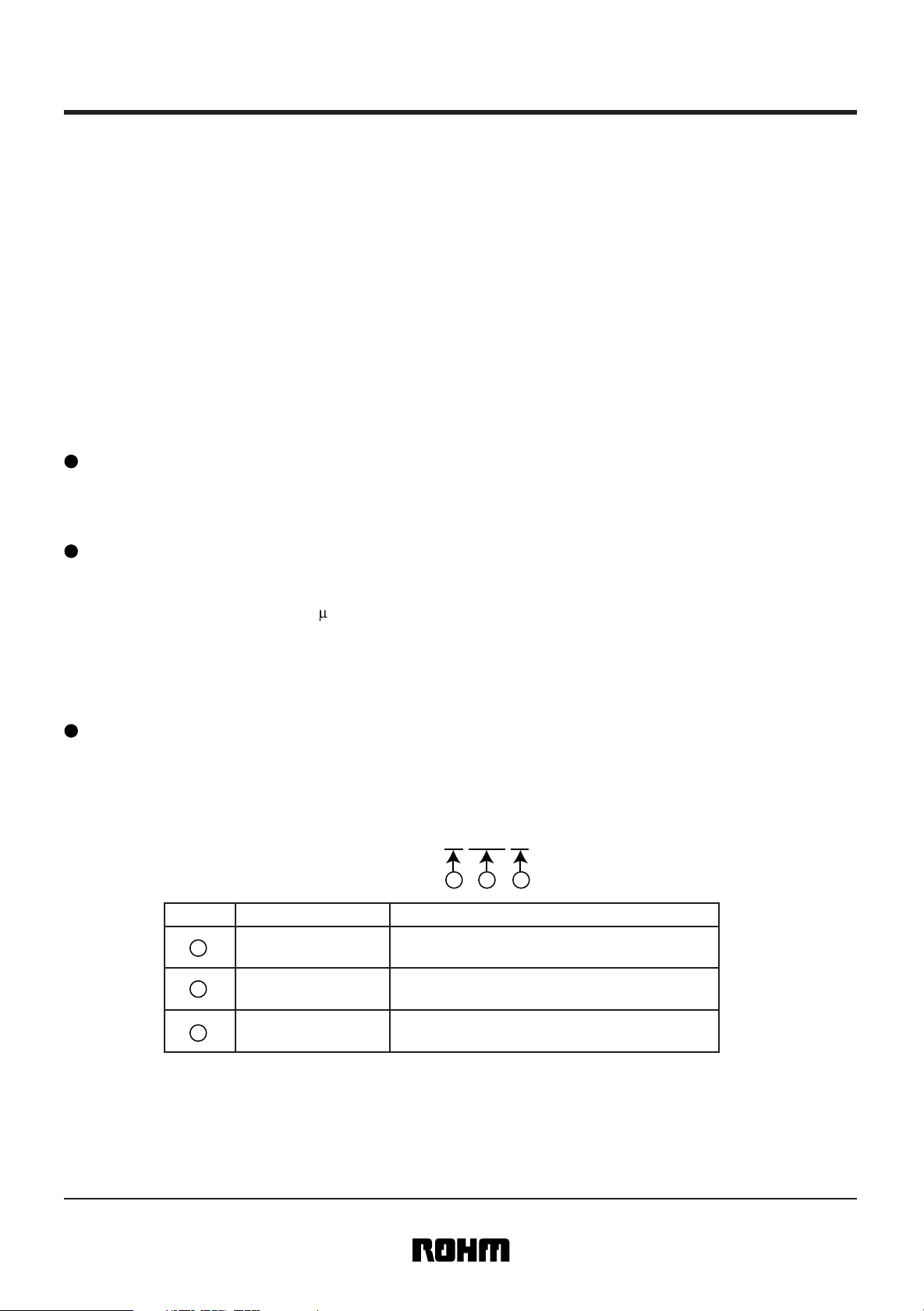
Pin layout
Pin layout of VSOF5(EMP5) and SSOP5(SMP5C2) is different as shown below. (Fig.1, Fig.2)
When used as replacement, please consider the difference. (The detail of packages is shown at P14.)
BD48XXG/BD49XXG
BD48XXFVE/BD49XXFVE
1VOUT VDD
2SUB
3N.C. GND
VSOF5
(EMP5)
Package
1.2mm
5
1.6mm
4
VDD
GND
1VOUT N.C.
SSOP5
(SMP5C2)
2
Package
3
1.6mm
5
2.9mm
4 N.C.
Fig.1 Fig.2
(Note) Connect SUB pin with GND pin.
Rev.A
2/15
Page 3
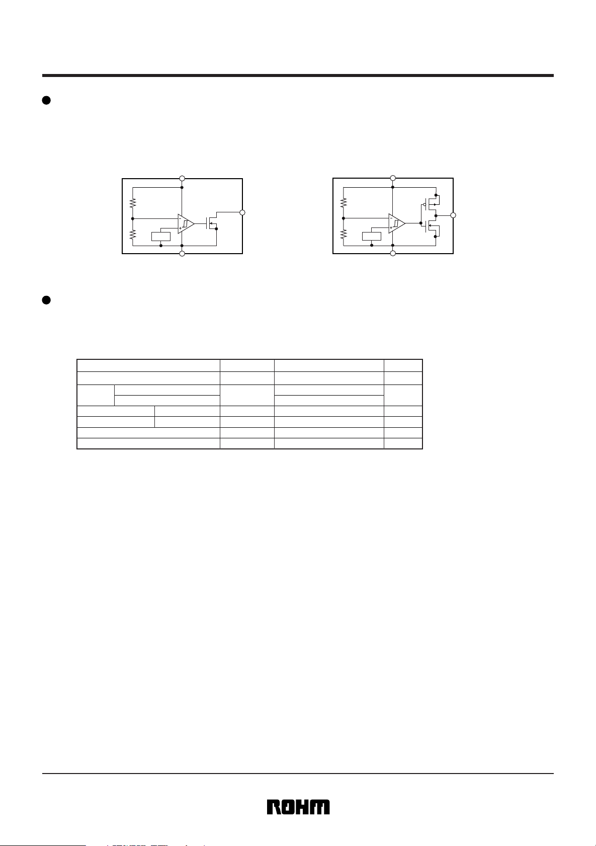
BD48XXG/FVE
Voltage detectors
Block diagram
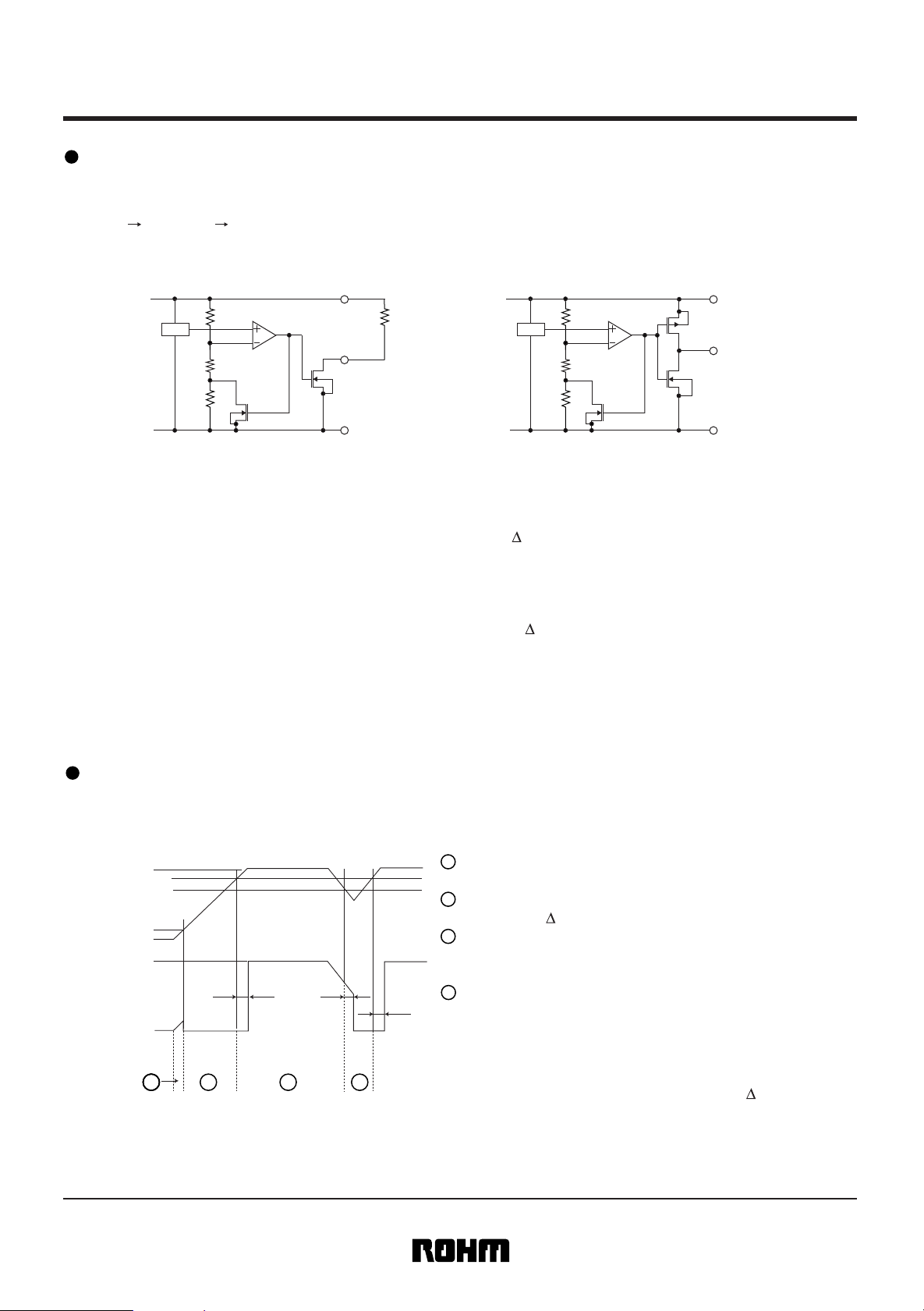
Two output types can be used. One is BD48XXG/FVE (Fig.3) of open drain output type, and the other is
BD49XXG/FVE (Fig.4) of CMOS output type.
BD48XXG/FVE : Open drain output BD49XXG/FVE : CMOS output
VDD
VDD
BD49XXG/FVE
Vref
GND
VOUT
Vref
GND
Fig.4Fig.3
VOUT
Absolute maximum rating (Ta=25°C)
To prevent the functional deterioration or thermal damage of semiconductor devices and ensure their service
life and reliability, they must be designed and reviewed in such a way that the absolute maximum rating can
not be exceeded in any cases or even at any moment.
Parameter Symbol Unit
Power supply voltage
Output
voltage
Power dissipation SSOP5 (SMP5C2)
Power dissipation VSOF5 (EMP5)
Nch Open drain output
CMOS output
*
*
*
*
Operating temperature
Storage temperature
*1 Derating : 1.5mW/°C for operation above Ta=25°C
*2 Derating : 1.0mW/°C for operation above Ta=25°C
*3 When only IC is used.
VDD – GND
VOUT
1
3
2
3
GND – 0.3 to VDD + 0.3
Pd
Pd
Topr
Tstg
Limits
– 0.3 to + 10
GND – 0.3 to + 10
150
100
– 40 to + 85
– 55 to + 125
V
V
mW
mW
°C
°C
• Power supply voltage
This voltage is the applied voltage between VDD and GND. The applied voltage should not exceed the
indicated value.
• Output voltage
VOUT pin voltage should not exceed the indicated value. For Nch open drain output type, VDD applied
voltage and VOUT pin H output voltage can be used independently. Both of them should not exceed the
each indicated value.
• Operating temperature range
The circuit function is guaranteed within the temperature range. However, the operating characteristics
are different from that of Ta=25°C. If they are any questions about the extent of guarantee of circuit
functions in this operating temperature range, please ask for more technical information.
• Storage temperature range
This IC can be stored up to this temperature range without deterioration of characteristics. However,
an abrupt thermal shock of extreme temperature fluctuations may cause the deterioration of characteristics.
Rev.A
3/15
Page 4
BD48XXG/FVE
Voltage detectors
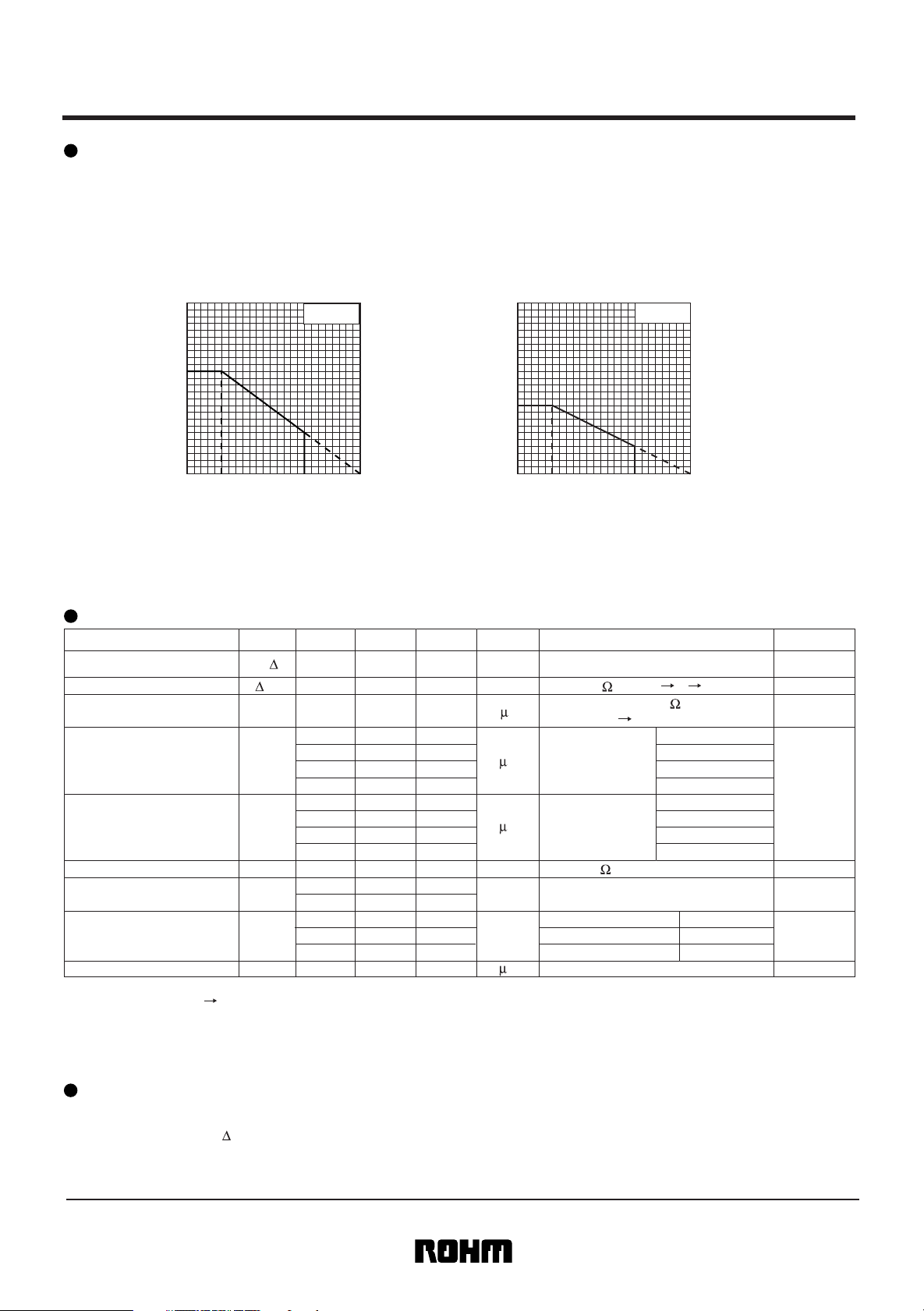
Power dissipation
Power consumption of the IC
Circuit current at ON/OFF is very small. Power consumption in output depends on each load connected with
VOUT pin. Please note that total power consumption must be within a power dissipation range in the secure
area of the entire operating temperature. Power dissipation of these packages; SSOP5 (SMP5C2) package
(BD48XXG/BD49XXG) Fig.5, and VSOF5 (EMP5) package (BD48XXFVE/BD49XXFVE) Fig.6 is shown below.
SSOP5 (SMP5C2) package
200
BD48XXG
BD49XXG
EMP5 (VSOF5) package
200
BD48XXFVE
BD49XXFVE
BD49XXG/FVE
150
100
Power dissipation (mW)
50
25 50
0
Ambient temperature Ta(°C)
Fig.5 Thermal derating curve Fig.6 Thermal derating curve
75 100 125
150
100
Power dissipation (mW)
50
0
25 50
Ambient temperature Ta(°C)
75 100 125
When it is used in the ambient temperature of (Ta)=25°C and more, make reference to each thermal derating
characteristics of used package. Both Fig.5 and Fig.6 show these characteristic when only IC is used.
Electrical characteristics (Unless otherwise noted; Ta=-25°C to 85°C)
Symbol Min. Max. Unit Conditions
Detection voltage
temperature coefficient
Hysteresis voltage
"H" transfer delay time
VS/ T
VS
TPLH
— ±100 ±360 ppm/°C
VS X 0.03 VS X 0.05 VS X 0.08
—
—
100
V
RL=470k , VDD=L H L
CL=100pF, RL=100k
s
VOUT=GND 50% *1
— 0.51 1.53 VS=2.3 to 3.1V
Circuit current when ON
ICC1
— 0.56 1.68
—
0.60
1.80
— 0.66 1.98 VS=5.3 to 6.0V
A
VDD=Vs–0.2V
*1
— 0.75 VS=2.3 to 3.1V2.25
Circuit current when OFF
ICC2
—
—
—
0.95 — — VVOPLMin. operating voltage RL=470k , VOL 0.4V *1
0.4 1 — VDS=0.5V, VDD=1.2V
2.0 4 —
0.7 1.4
0.9 1.8 —
1.1 2.2 —
Output leak current
*1 Operation is guaranteed forTa=25°C.
*2 TPLH : VDD=(VS typ.–0.5V) (VS typ.+0.5V).
Note) RL is not necessary for CMOS output type.
Note) Minimum operating voltage
VOUT output becomes inconsistent if the VDD is equal to or lower than the operating limit voltage. It goes open, H, or L.
Note) Hysteresis voltage=(Reset release voltage)-(Reset detection voltage) [V]
Ileak
—
0.80
0.85
0.90
—
2.40
2.55
2.70
—
0.1
VDD=Vs+2V
A
*1
>
-
mAIOL"L" output current
VDS=0.5V, VDD=2.4V (VS 2.7V)
VDS=0.5V, VDD=4.8V
mAIOH"H" output current
VDS=0.5V, VDD=6.0V VS=4.3 to 5.2V
VDS=0.5V, VDD=8.0V VS=5.3 to 6.0V
VDD=VDS=10V *1
A
*2
VS=3.2 to 4.2V
VS=4.3 to 5.2V
VS=3.2 to 4.2V
VS=4.3 to 5.2V
VS=5.3 to 6.0V
>
-
VS=2.3 to 4.2V
ReferenceTap.Parameter
Fig.12,13
15,17
Fig.33
Fig.31
Fig.28
Fig.31
Fig.29
Fig.30
Fig.32
Term explanation
• Detection voltage (VS) : VDD voltage when the output (Vout) goes from "H" to "L".
• Release voltage (VS+ VS) : VDD voltage when output (Vout) goes from "L" to "H".
• Hysteresis voltage : The difference between detection voltage and release voltage. Malfunction due to noise in VDD
(within hysteresis voltage) could be avoided by hysteresis voltage.
Rev.A
4/15
Page 5
BD48XXG/FVE
Voltage detectors
Operating explanation
Ex.) For both open drain type (Fig.7) and CMOS output type (Fig.8), detection voltage and release voltage are
threshold voltage. When voltage applied to VDD pin reaches each threshold voltage, VOUT pin voltage goes
"H" "L" or "L" "H". BD48XXG/FVE series are open drain types and pull-up resistor must be connected
to VDD, or other power supply. (In this case, output (VOUT) H voltage is VDD, or other power supply voltage.)
BD49XXG/FVE
VDD
Vref
R1
R2
R3 Q1
GND
Fig.7 (BD48XX type Internal block diagram) Fig.8 (BD49XX Internal block diagram)
RL
Vref
VOUT
R1
R2
R3 Q1
VDD
Q2
VOUT
GND
• SWEEP DOWN for VDD
When VDD is equal to or more than the release voltage (Vs+ Vs), output VOUT is in "H" mode. (Nch output
transistor Q1 is OFF, Pch output transistor Q2 is ON.) When VDD is gradually decreased, output (VOUT)
turns "L" in the detection voltage (Vs). (Nch output transistor Q1 is ON, Pch output transistor Q2 is OFF.)
• SWEEP UP for VDD
When VDD is equal to or lower than the detection voltage (Vs+ Vs), output VOUT is in "L" mode. (Nch output
transistor Q1 is ON, Pch output transistor Q2 is OFF.) When VDD is gradually increased, output (VOUT) turns
"H" in the release voltage (Vs). (Nch output transistor Q1 is OFF, Pch output transistor Q2 is ON.)
• Some hysteresis is given such a way that the release voltage is the detection voltage X (1.05 Typ.).
• The output becomes inconsistent if the VDD is equal to or lower than the operating limit voltage.
Timing waveform
Ex.) The relation between input voltage VDD and output voltage VOUT when VDD is increased and decreased
is shown below. (Circuit is shown above. Fig7, 8)
1
VDD
VOUT
VDD
VS+ VS
D
VS
VOPL
0V
VOH
If the VDD is equal to or lower than the operating limit
voltage (VOPL) at power-up, the output is inconsistent.
2
When the VDD is equal to or lower than the reset release
voltage (Vs+ Vs), VOUT=L.
3
When VDD exceeds the Reset Release Voltage, VOUT
turns H with a delay of TPLH. See Fig. 15 and 17 for the
reference waveform.
TPLH
VOL
TPHL
TPLH
4
If the VDD goes below the detection (Vs) at power-down
or instantaneous power failure, VOUT turns L with a delay
of TPHL.
See Fig.16 and 18 for the reference waveform.
2 3 4111
Fig.9
The potential difference between the detection voltage
and the release voltage is called hysteresis ( Vs).
The products are designed so as to prevent power supply
fluctuation within this hysteresis from causing fluctuation
in output in order to avoid malfunction due to noise.
Rev.A
5/15
Page 6

Voltage detectors
Application circuit
1)Application circuit as ordinal supply detection reset is shown below.
BD48XXG/FVE
BD49XXG/FVE
VDD1
BD48XXX
RL
( )
CL
(Noise filtering
capacitor)
RST
Micro
controller
VDD2
GND
VDD1
GND
BD49XXX
( )
CL
RST
(Noise filtering
capacitor)
Micro
controller
Fig.10 Open collector output type Fig.11 CMOS output type
Output type of BD48XXG/FVE series (Open drain type) and BD49XXG/FVE series (CMOS type) is different.
An example of usage is shown below.
• When the power supply of microcontroller (VDD2) and power supply for the reset detection (VDD1) is different.
Provide RL for the output of a product with open drain output (BD48XXG/FVE series) on the VDD2 side,
as shown in Fig.10.
• When the power supply of microcontroller and that of reset is same (VDD1).
A product with CMOS output (BD49XXG/FVE series) can be used as shown in Fig.11. Or if RL is provided
with open drain output (BD48XXG/FVE series) on the VDD1 side, it can be used.
When the capacitor CL for noise filtering and for delay time setting is connected to VOUT pin (reset signal input
pin of microcontroller), make a setting in consideration of the wave rounding of the rise and fall of VOUT.
(See the delay shown in Fig.14 as the reference.)
10000
1000
( s)
100
delay time
10
Output delay time "L H"
[BD4842G/FVE]
1000100
CL Capacitance
(pF)
80
79
78
77
76
( s)
75
74
73
delay time
72
71
70
10000
5V
Output delay time "H L"
[BD4842G/FVE]
1000100
CL Capacitance
(pF)
10000
5V
Release voltage
(VS+ VS)
VDD
VOUT
VDD
VOUT
VS±0.5V
GND
Fig.12
TPLH
Fig.14 Delay time I/O condition
RL=100K
CL
0.5V
0.5V
TPHL
RL=100K
CL
VS±0.5V
VDD
VOUT
GND
Fig.13
Detection voltage VS [V]
5V
VOUT=5V X 0.5 [V]
Rev.A
6/15
Page 7

Voltage detectors
• Test data
BD48XXG/FVE
BD49XXG/FVE
VDD
VOUT
VDD
TPLH
TPLH
Fig.15
BD4845G TPLH output waveform
VDD
VOUT
TPHL
Fig.16
BD4845G TPHL output waveform
VDD
VOUT
VOUT
T
PLH
Fig.17
BD4945G TPLH output waveform
Reference data : BD4845G test data
RL=100k
CL=100pF
Reference data : BD4945G test data
CL=100pF
TPHL
Fig.18
BD4945G TPHL output waveform
100k
VDD
BD4845G
VDD VOUT
BD4945G
VOUT
100pF
GND
100pF
GND
Rev.A
7/15
Page 8

BD48XXG/FVE
Voltage detectors
2)Application circuit when microcontroller is reset with OR connection of the two types of the detection voltage
is shown below.
BD49XXG/FVE
VDD1
BD48XXX
VDD2
BD48XXX
Fig.19
RL
RST
Micro
controller
VDD3
GND
When there is more than one system power supply and it is necessary to individually monitor the power supply
(VDD1, VDD2) to reset the microcontroller, open drain output type BD48XXG/FVE series can be connected to
form an OR circuit as shown in Fig.19 for pulling up to an arbitrary voltage (VDD3) to adjust the H voltage of the
output to the microcontroller power supply (VDD3).
3)Application circuit when it is used as Power-on reset is shown below.
(However, it can be used for only BD48XXG/FVE series.)
VDD
Di
R
BD48XXX
C
Fig.20
RL
Micro
controller
GND
If the power supply voltage is lower than the guaranteed range, power-on reset of the microcontroller is necessary
to prevent program runaways and unwanted memory register updates. A power-on reset circuit used with
BD48XXG/FVE series (Nch open drain) is shown in Fig.20. C and R conneceted to VDD pin of RESET IC make
the wave rounding of the VDD pin and generate input signal with time constant. When the input power supply is
fallen, the electric charge of the capacitor is discharged through Di connected between VDD pin and VDD.
The value of the resister R should be enough to prevent malfunction caused by circuit current through
BD48XXG/FVE series. Set in such a way that the following expression stands:
Hysteresis > R X { (Circuit current at ON) - (Circuit current at OFF) }
Do not use BD49XXG/FVE series (CMOS output) for the power-on reset because malfunction may occur.
(Oscillation at output etc.) The feed through current (CMOS output) at detection may cause malfunction
mentioned above. (Feed through current is the current flowed from VDD into GND instantly when output
goes "H" "L". )
VDD
Feed through current
VOUT
GND
Fig.21
CMOS output circuit
ICC
Feed through current
0 VDD
VS
Fig.22
Current consumption Vs. power supply voltage
Rev.A
8/15
Page 9

BD48XXG/FVE
Voltage detectors
Establishment of RESET transfer delay time
Delay time at the rise and fall of VDD can be established by RL, CL connected to VOUT pin.
• Delay time at the rise of VDD TPLH : Time until when VOUT is 1/2 of VDD after the rise of VDD, and beyond
the release voltage (Vs+ Vs).(See P7). It is the total time established
by IC internal transfer delay time TD and external RL, and CL.
RESET pin voltage
VDD
VDD
BD49XXG/FVE
OUT
RL
RESET
63%
50%
=CL X RL
Output Tr
OFF
CL
VOUT voltage [V]
0 t
0.69 X
Fig.24 RESET pin voltageFig.23
Time
If the threshold voltage of the RESET terminals is 1/2 of VCC, delay time TPLH at the rise of VDD is shown
in the expression below.
TPLH=0.69 X CL X RL+TD
TD=Internal circuit delay of BD48XX : About 35 s (typ.) VDD=(Vs–0.5V) (Vs+0.5V)
CL : Capacity of external capacitor beween VOUT pin and GND
RL : External resistance between VOUT pin and power supply
• Delay time at the fall of VDD TPHL : Time until when VOUT is 1/2 of VDD after across the detection
voltage (Vs).(See P7). It is the total time established by IC internal
transfer delay time TD and external RL, and CL.
VDD
Vs
Vout voltage[V]
0 t
Fig.26 RESET pin voltage
B
A
Time
Output Tr
ON
VOUT
IOL
VDD
RL
RESET
CL
Fig.25
=A+B
PHL
T
A = About 70 s(Typ.) :
B =
IOL
C
CL X Vs
Capacity of external capacitor beween
L :
:
Delay time by external C
Internal IC transfer delay time of
VOUT pin and GND
Vs : Detection voltage
: "L" output current of BD48XX
OL
I
Make sure to test in actual because it depends
on detection voltage.
Reference:V
=2.4V, VDD
S
L
, R
L
=About 8mA at A:typ.
VDD
VOUT
BD4842
Release voltage
(VS+ VS)
0.5V
0.5V
TPLH
Fig.27 Delay time I/O condition
TPHL
Rev.A
Detection voltage VS [V]
5V
VOUT=5V X 0.5 [V]
9/15
Page 10

Voltage detectors
Characteristic data (Reference data)
BD48XXG/FVE
BD49XXG/FVE
1.5
1.0
[ A]
DD
I
0.5
[V]
VOUT
[BD4842G/FVE]
0
A
VDD
521 43 1076 98
[V]
VDD
VDD
GND
VOUT
Fig.28
Circuit current
9
8
7
6
5
4
3
2
1
Ta=25°C
0
VDD
[V]
[BD4842G/FVE]
Ta=25°C
3.50.5 1.5 2.5 3 4.54 5.5521
18
15
10
mA]
[
IOL
5
0.5 1
0
VDD
Fig.29
"L" output current
4
3
2
1
0
-1
Ileak [ A]
-2
-3
-4
2 4
0
[BD4842G/FVE]
VDD=2.4V
VDD=1.2V
1.5 2 2.5
[V]
VDS
VDD
VOUT
GND
[BD4842G/FVE]
6 8 10 12
[V]
VDS
A
VDS
45
40
35
30
25
[mA]
20
IDS
15
10
5
1 2
0
VDD
Fig.30
"H" output current
[BD4942G/FVE]
=8.0V
DD
V
=6.0V
DD
V
VDD=4.8V
3 4 5 6
[V]
VDS
VDD
GND
A
VOUT
VDS
VDD
VDD
VOUT
GND
Fig.31
I/O characteristic
RL=470K
V
VDD
VDD
GND
Fig.32
Output leak current
VOUT
A
VDS
Rev.A
10/15
Page 11

Voltage detectors
BD48XXG/FVE
BD49XXG/FVE
low to high(VS+ VS)
[°C]
Ta
VDD
VOUT
GND
[BD4842G/FVE]
high to low(VS)
VDD
[V]
VS
5.4
5.0
4.6
4.2
3.8
3.4
0 50–40
Fig.33
Detection voltage (VS)
Release voltage (VS+ VS)
RL=470K
V
[BD4842G/FVE]
1.0
[ A]
DD
I
0.5
90
-40
A
VDD
20-20 0 10040 8060
[°C]
Ta
VDD
GND
Fig.34
Circuit current on ON (VS-0.2V)
VOUT
[BD4842G/FVE]
1.0
[ A]
DD
I
0.5
-40
A
VDD
20-20 0 10040 8060
[°C]
Ta
VDD
VOUT
GND
Fig.35
Circuit current on OFF (VS+0.2V)
[BD4842G/FVE]
2
1
[ A]
0
leak
I
-1
-2
-20 100
-40
VDD
200 40 8060
[°C]
Ta
VDD
VOUT
GND
Fig.36
Output leak current
[BD4842G/FVE]
1.0
[V]
OPL
0.5
V
-40
VDD
A
VDS
20-20 0 40 8060
[°C]
Ta
VDD
VOUT
GND
100
RL=470K
V
Fig.37
Operating limit voltage
Rev.A
11/15
Page 12

Voltage detectors
Taping specification
1)Dimension of tape
BD48XXG/FVE
BD49XXG/FVE
Rectangular recess to hold a component
B
t
K
Package SSOP5 (SMP5C2)
Circular feed hole
D1
A
Fig.38
P2
P0
P1
D0
E
F
W
(mm)
Symbol
Dimension
Symbol
Dimension
Package VSOF5 (EMP5)
Symbol
Dimension
Symbol
Dimension
A
3.2±0.1
P2
2.0±0.05t0.3±0.05K1.3±0.1W8.0±0.2
A
1.83±0.1B1.83±0.1
P2
2.0±0.05t0.25±0.05K0.75±0.1
B
3.1±0.1
1.5
1.5
D0
+0.1
–0
D0
+0.1
–0
D1
1.1±0.1
D1
0.5±0.1
W
8.0±0.2
E
1.75±0.1
E
1.75±0.1
F
3.5±0.05P04.0±0.1
F
3.5±0.05P04.0±0.1
P1
4.0±0.1
(mm)
P1
4.0±0.1
Rev.A
12/15
Page 13

Voltage detectors
BD48XXG/FVE
BD49XXG/FVE
2)Dimension of reel
TMAX
E
D
C
B
Symbol
DimensionA180 Max.B60±2.0
A
C
13.0±0.5
Fig.39
D
20.2 Min.
E
1.5 Min.
W
9.0±0.3
t
W
Label side(1.0)
Back side(1.2)
t
TMax.
17.4
3)Standard packaged quantity and IC direction
The standard packaged quantity is 3,000 pcs/reel. Orders should be in multiples of the standard packaged
quantity. The ICs are TR oriented (as shown below).
First pin
(mm)
Fig.40
(Leader side)
Rev.A
13/15
Page 14

Voltage detectors
Recommended mounting conditions
• SSOP5 (SMP5C2) allows either reflow or flow soldering mounting.
• VSOF5 (EMP5) allows reflow mounting.
The mounting conditions are shown below.
BD48XXG/FVE
BD49XXG/FVE
1)Reflow
Up to two reflows are allowed.
2)Flow soldering
Treatment
140°C
process
Preheating
section
Solder bath
90±30s
Condition
Temperature
150±10°C
Max. 260°C
Max. 10s
Max.240°C
235°C
160°C
Fig.41
Time
60 to 120s
Max. 10s
3)Product storage conditions
Store the products in an environment of 5 to 30°C in temperature and 70% RH or lower in humidity.
Dimension
0.42
0.1
(UNIT:mm)
4° + 6°
-4°
0.2MIN
+0.05
0.13
–0.03
+0.05
-0.04
1.6±0.05
0.6MAX
1.2±0.05
1.6±0.05
1.0±0.05
4
5
3
1
2
Lot No.
0.22±0.05
0.5
VSOF5
(EMP5)
(UNIT:mm)
0.13±0.05
0.08
M
0.2MAX
0.2
±
2.8
0.2
+
0.1
-
1.6
2.9±0.2
(5)
(4)
(2)(1)
(3)
0.05
1.1±
1.25MAX
0.95
0.05
±
0.05
(SMP5C2)
SSOP5
Rev.A
14/15
Page 15

Voltage detectors
Reference land pattern
BD48XXG/FVE
BD49XXG/FVE
VSOF5
(EMP5)
SSOP5
(SMP5C2)
e e
e1
2
b2
2
e e
e1
b2
Fig.42 Fig.43
Lead pitcheLead pitch
e1
Land length
2
0.50 1.35 0.35 0.25
Unit:mm
Land width
b2
Lead pitcheLead pitch
e1
Land length
2
0.95 2.40 1.00 0.60
Unit:mm
Land width
b2
For actual designing, take the board density, mountability, dimension tolerance, etc. for optimization.
Part number and marking of samples
The BD48XX and BD49XX series products allow optimum selection of detection voltage, output circuit type
and package according to the application.
Part No. Specification Contents
Part No.
B D 4 X X X X
1 2 3
Marking Voltage Part No. Marking Voltage Part No. Marking Voltage Part No. Marking Voltage Part No.
BD4860EW
EV
EU
ET
ES
ER
EQ
EP
EN
EM
EK
EH
EG
EF
EE
ED
EC
6.0V
5.9V
BD4859
BD4858
5.8V
5.7V
BD4857
5.6V
BD4856
BD4855
5.5V
BD4854
5.4V
5.3V
BD4853
5.2V
BD4852
5.1V
BD4851
BD4850EL
5.0V
4.9V
BD4849
4.8V
4.7V
4.6V
4.5V
4.4V
4.3V
4.2V
BD4848
BD4847
BD4846
BD4845
BD4844
BD4843
BD4842
EJ
EB
EA
DV
DU
DT
DS
DR
DQ
DP
DN
DM
DL
DK
DJ
DH
DG
DF
DE
DD
4.1V
4.0V
3.9V
3.8V
3.7V
3.6V
3.5V
3.4V
3.3V
3.2V
3.1V
3.0V
2.9V
2.8V
2.7V
2.6V
2.5V
2.4V
2.3V
1
2
3
BD4841
BD4840
BD4839
BD4838
BD4837
BD4836
BD4835
BD4834
BD4833
BD4832
BD4831
BD4830
BD4829
BD4828
BD4827
BD4826
BD4825
BD4824
BD4823
Output circuit type
Detection voltage
Package
GW
6.0V
GV
GU
GT
GS
GR
GQ
GP
GN
GM
GL
GK
GJ
GH
GG
GF
GE
GD
GC
BD4960
5.9V
BD4959
BD4958
5.8V
5.7V
BD4957
5.6V
BD4956
BD4955
5.5V
BD4954
5.4V
5.3V
BD4953
5.2V
BD4952
5.1V
BD4951
5.0V
BD4950
4.9V
BD4949
BD4948
4.8V
4.7V
BD4947
4.6V
BD4946
BD4945
4.5V
4.4V
BD4944
4.3V
BD4943
4.2V BD4942
8 : Open drain output
9 : CMOS output
Ex : VS : described in each 0.1V step
for 2.3V to 6.0V range (29 means 2.9V)
G : SSOP5 (SMP5C2)
FVE : VSOF5 (EMP5)
4.1V
GA
4.0V
FV
3.9V
FU
3.8V
FT
3.7V
FS
3.6V
FR
3.5V
FQ
3.4V
FP
3.3V
FN
3.2V
3.1V
FL
3.0V
FK
2.9V
FJ
2.8V
FH
2.7V
FG
2.6V
FF
2.5V
FE
2.4V
FD
2.3V
BD4941GB
BD4940
BD4939
BD4938
BD4937
BD4936
BD4935
BD4934
BD4933
BD4932
BD4931FM
BD4930
BD4929
BD4928
BD4927
BD4926
BD4925
BD4924
BD4923
BD48XXG/BD49XXG
SSOP5 (SMP5C2)
(5)
(1)
(4)
(2)
(3)
Mark
BD48XXFVE/BD49XXFVE
VSOF5 (EMP5)
(5)
(1)
(4)
(2)
(3)
Lot.No
Mark
Lot.No
Rev.A
15/15
Page 16

Appendix
No technical content pages of this document may be reproduced in any form or transmitted by any
means without prior permission of ROHM CO.,LTD.
The contents described herein are subject to change without notice. The specifications for the
product described in this document are for reference only. Upon actual use, therefore, please request
that specifications to be separately delivered.
Application circuit diagrams and circuit constants contained herein are shown as examples of standard
use and operation. Please pay careful attention to the peripheral conditions when designing circuits
and deciding upon circuit constants in the set.
Any data, including, but not limited to application circuit diagrams information, described herein
are intended only as illustrations of such devices and not as the specifications for such devices. ROHM
CO.,LTD. disclaims any warranty that any use of such devices shall be free from infringement of any
third party's intellectual property rights or other proprietary rights, and further, assumes no liability of
whatsoever nature in the event of any such infringement, or arising from or connected with or related
to the use of such devices.
Upon the sale of any such devices, other than for buyer's right to use such devices itself, resell or
otherwise dispose of the same, no express or implied right or license to practice or commercially
exploit any intellectual property rights or other proprietary rights owned or controlled by
ROHM CO., LTD. is granted to any such buyer.
Products listed in this document are no antiradiation design.
Notes
The products listed in this document are designed to be used with ordinary electronic equipment or devices
(such as audio visual equipment, office-automation equipment, communications devices, electrical
appliances and electronic toys).
Should you intend to use these products with equipment or devices which require an extremely high level of
reliability and the malfunction of with would directly endanger human life (such as medical instruments,
transportation equipment, aerospace machinery, nuclear-reactor controllers, fuel controllers and other
safety devices), please be sure to consult with our sales representative in advance.
About Export Control Order in Japan
Products described herein are the objects of controlled goods in Annex 1 (Item 16) of Export Trade Control
Order in Japan.
In case of export from Japan, please confirm if it applies to "objective" criteria or an "informed" (by MITI clause)
on the basis of "catch all controls for Non-Proliferation of Weapons of Mass Destruction.
Appendix1-Rev1.1
 Loading...