

Page 1
High-accuracy
Low current consumption
General-purpose
5
4
RESET IC
BD47XXG series
Description
BD47XXG is a series of RESET ICs developed to prevent
system error at transient state when the power of CPU and
logic circuit switches ON/OFF or shutdown. These ICs consist
of Power, GND, and reset output to detect power supply voltage
of various systems and to output reset signal. These ICs are
more practical for portable products because of their ultra-small
package and low current consumption.
Features
1) Detection voltage: 0.1V step line up 1.9~4.6V(Typ.)
2) High-accuracy voltage detection Vs±2%(Max.)
3) Low current consumption
4) "L" reset output of open collector
5) Small SMP5 package
Applications
Portable products, Equipments with CPU and logic circuit
Series characteristics
Part No.
Detection voltage Vs (V)
Min
4.508BD4746G 50 15 SMP5
4.116BD4742G 50 15 SMP5
Typ.
4.600
4.500 4.590 1.54.410BD4745G 50 15 SMP5
4.400 4.488 1.54.312BD4744G 50 15 SMP5
4.300 4.386 1.54.214BD4743G 50 15 SMP5
4.200 4.284 1.5
4.100 4.182 1.54.018BD4741G 50 15 SMP5
4.000 4.080 1.53.920BD4740G 50 15 SMP5
3.900 3.978 1.53.822BD4739G 50 15 SMP5
3.800 3.876 1.53.724BD4738G 50 15 SMP5
3.700 3.774 1.53.626BD4737G 50 15 SMP5
3.600 3.672 1.53.528BD4736G 50 15 SMP5
3.500 3.570 1.53.430BD4735G 50 15 SMP5
3.400 3.468 1.53.332BD4734G 50 15 SMP5
3.300 3.366 1.53.234BD4733G 50 15 SMP5
3.200 3.264 1.53.136BD4732G 50 15 SMP5
3.100 3.162 1.53.038BD4731G 50 15 SMP5
3.000 3.060 1.52.940BD4730G 50 15 SMP5
2.900 2.958 1.52.842BD4729G 50 15 SMP5
2.800 2.856 1.52.744BD4728G 50 15 SMP5
2.700 2.754 1.52.646BD4727G 50 15 SMP5
2.600 2.652 1.52.548BD4726G 50 15 SMP5
2.500 2.550 1.52.450BD4725G 50 15 SMP5
2.400 2.448 1.52.352BD4724G 50 15 SMP5
2.300 2.346 1.52.254BD4723G 50 15 SMP5
2.200 2.244 1.52.156BD4722G 50 15 SMP5
2.100 2.142 1.52.058BD4721G 50 15 SMP5
2.000 2.040 1.51.960BD4720G 50 15 SMP5
1.900 1.938 1.51.862BD4719G 50 15 SMP5
Max.
4.692
Consumption
current (µA Typ.)
I
CCL
1.5
I
CCH
1.6
1.6
1.6
1.6
1.6
1.6
1.6
1.6
1.6
1.6
1.6
1.6
1.6
1.6
1.6
1.6
1.6
1.6
1.6
1.6
1.6
1.6
1.6
1.6
1.6
1.6
1.6
1.6
0.2
±
2.8
1.25MAX
Hysteresis
voltage (mV)
1
2
3
2.9±0.2
(5)
(4)
0.2
0.1
–
+
1.6
(2)(1)
(3)
±
0.05
1.1
0.95
0.05
±
0.05
SMP5
Operating output
current (mA)
0.42
0.1
0.05
+
0.04
–
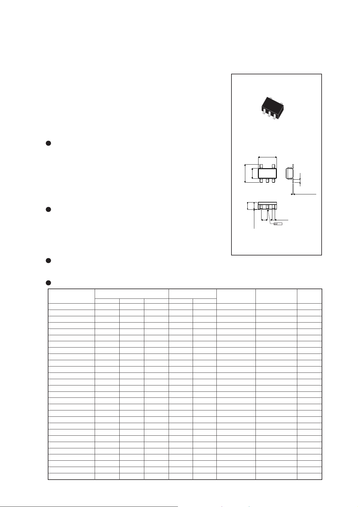
1pin : N.C.
2pin : SUB
3pin : GND
4pin : Vout
5pin : Vcc
(UNIT:mm)
0.2MIN
0.05
+
0.13
0.03
–
Package
Page 2
Absolute Maximum Ratings(Ta=25˚C)
Parameter Symbol Unit
Power supply voltage
Output voltage
Power dissipation (SMP5)
Operating temperature range
Storage temperature range
Note) The ratings shown above indicate breakdown limit of the pin and should not be regarded as the values that guarantee the operation.
Vcc
Po
Pd
Topr
Tstg
* Derating : 1.5mW/˚C for operation above Ta=25˚C
Limits
–0.3 ~ +10
–0.3 ~ +10
*
150
–20 ~ +75
–40 ~ +125
V
V
mW
˚C
˚C
Electrical characteristics(Unless otherwise noted; Ta=25˚C)
Symbol Min. Max. Unit ConditionsTyp.Parameter
Detection voltage Vs –2%
Detection voltage
temperature coefficient
Hysteresis voltage
"H" transfer delay time
"L" transfer delay time
"L" output voltage
Circuit current (At ON mode)
Circuit current (At OFF mode)
Operating limit voltage
Output leak current
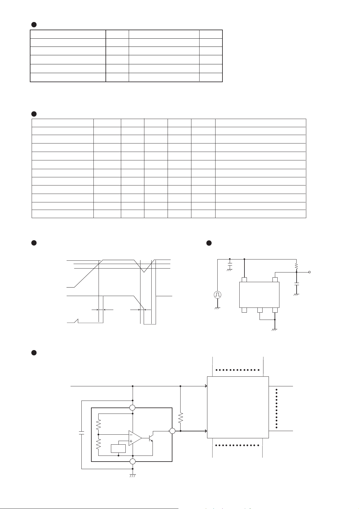
*1 TPLH : Vcc=(Vs typ.–0.4V)Æ(Vs typ.+0.4V)
*2 TPHL : Vcc=(Vs typ.+0.4V)Æ(Vs typ.–0.4V)
Vs/∆T
∆Vs
TPLH
TPHL
VOL
Icc1
Icc2
VOPL
IL
—
30
—
—
—
—
—
—
—
1.9~4.6
±0.01
50
20
60
0.1
1.5
1.6
0.65
—
+2%
—
100
50
120
0.4
3.0
3.2
0.85
0.1
V
%/˚C
mV
µS
µS
V
µA
µA
V
µA
RL=4.7kΩ, Vcc=HÆL
RL=4.7KΩ, Ta=–20~+75˚C
RL=4.7KΩ, Vcc=LÆHÆL
CL=100PF, RL=4.7KΩ
CL=100PF, RL=4.7KΩ
Vcc=VsMIN.–0.05V, RL=4.7KΩ
Vcc=VsMIN.–0.05V, RL=∞
Vcc=VsTYP./0.85V, RL=∞
RL=4.7KΩ, VOL≥0.4V
Vcc=Vout=10V
3.0 15.0 — mAIOL"L" output current Vo=0.4V, Vcc=VsMIN.–0.05V
*1
*2
Timing waveform Transfer delay time measurement circuit
VCC
VOUT
VCC
VS+∆VS
VS
0V
VOH
VOL
TPLH
TPHL
VCC
0.22uF
5 4
Vcc Vout
BD47XXG
NC SUB GND
1 2 3
RL=4.7KΩ
100pF
Application Circuit
VDD
5
VCC
Micro
controller
Vref
3
GND
BD47XXG
4
reset pin
Vout
Page 3

Characteristic diagram and Measurement circuit (When BD4729G is measured.)
Current consumption
10
9.5
9
8.5
8
7.5
7
6.5
6
5.5
5
4.5
Icc (µA)
4
3.5
3
2.5
2
1.5
1
0.5
0
0
0.5 1 1.5 2 2.5 3 3.5 4 4.5 5 5.5 6.5 7.5 8.5 9.56 7 9 108
V
A
Icc1=1.34µA
Icc2=1.46µA
Vcc (V)
10µF
Vcc
VOUT
BD4729G
GND
NC
6
I/O characteristic
5
4
3
Vout (V)
2
1
0
0
0.5 1 1.5 2 2.5 3 3.5 4 4.5 5 5.5 6
V V
Vs=2.9V Vs=2.95V
dVs=50mV
Vcc (V)
R=4.7K
Vcc
BD4729G
10µF
GND
VOUT
Operating limit voltage 'L' output current
1000
900
800
700
600
500
Vout (mV)
400
300
200
100
0
0
0.25 0.5 0.75 1 1.25 1.5 1.75 2 2.25 2.5 2.75
V V
VOPL=0.675V
Vcc (V)
10µF
R=4.7K
Vcc
BD4729G
GND
VOUT
800
700
600
500
400
Vout (mV)
300
200
100
0
0
2.5 5 7.5 10 12.5 15 17.5 20 22.5 27.525 30 32.5
IOL=12.194mA@Vo=400mV
Iol (mA)
Vcc
VOUT
BD4729G
10µF IOL
GND
A
V
Page 4

Setting of the RESET signal delay time
Delay time can be set by capacitor CL and resistance RL connected to the output pin as shown below.
CL is charged by RL when Vcc is rising. The delay time caused by charging is determined by the
time constant of CL, RL and the threshold voltage of RESET pin. RESET IC discharges CL forcedly
when Vcc is falling. The delay time of RESET signal is determined by adding the delay time of single
RESET IC to each time.
VCC
VS+∆VS
BD47XXG
Vcc
GND
Vout
RL
CL
V
DD
RESET
GND
VCC
CPU
Micro-controller
RESET
(=VOUT)
VS
0V
VOH
VOL
TPLH
TPHL
Part number and Marking of samples
TPLH
(5)
(1)
(2)
Marking
(4)
(3)
Lot.No
Marking Voltage
1.9V
BB
2.0V
BC
2.1V
BD
2.2V
BE
2.3V
BF
2.4V
BG
2.5V
BH
2.6V
B3
2.7V
BJ
2.8V
BK
BL
BM
BN
B4
BP
BQ
BR
BS
BT
Voltage
2.9V
3.0V
3.1V
3.2V
3.3V
3.4V
3.5V
3.6V
3.7V
3.8V
BD4729
BD4730
BD4731
BD4732
BD4733
BD4734
BD4735
BD4736
BD4737
BD4738
Part No. Part No. Part No.
BD4719BA
BD4720
BD4721
BD4722
BD4723
BD4724
BD4725
BD4726
BD4727
BD4728
Marking
Marking
BU
BV
BW
BX
BY
BZ
B1
B2
Voltage
3.9V
4.0V
4.1V
4.2V
4.3V
4.4V
4.5V
4.6V
BD4739
BD4740
BD4741
BD4742
BD4743
BD4744
BD4745
BD4746
Page 5

Appendix
No technical content pages of this document may be reproduced in any form or transmitted by any
means without prior permission of ROHM CO.,LTD.
The contents described herein are subject to change without notice. The specifications for the
product described in this document are for reference only. Upon actual use, therefore, please request
that specifications to be separately delivered.
Application circuit diagrams and circuit constants contained herein are shown as examples of standard
use and operation. Please pay careful attention to the peripheral conditions when designing circuits
and deciding upon circuit constants in the set.
Any data, including, but not limited to application circuit diagrams information, described herein
are intended only as illustrations of such devices and not as the specifications for such devices. ROHM
CO.,LTD. disclaims any warranty that any use of such devices shall be free from infringement of any
third party's intellectual property rights or other proprietary rights, and further, assumes no liability of
whatsoever nature in the event of any such infringement, or arising from or connected with or related
to the use of such devices.
Upon the sale of any such devices, other than for buyer's right to use such devices itself, resell or
otherwise dispose of the same, no express or implied right or license to practice or commercially
exploit any intellectual property rights or other proprietary rights owned or controlled by
ROHM CO., LTD. is granted to any such buyer.
Products listed in this document use silicon as a basic material.
Products listed in this document are no antiradiation design.
Notes
The products listed in this document are designed to be used with ordinary electronic equipment or devices
(such as audio visual equipment, office-automation equipment, communications devices, electrical
appliances and electronic toys).
Should you intend to use these products with equipment or devices which require an extremely high level of
reliability and the malfunction of with would directly endanger human life (such as medical instruments,
transportation equipment, aerospace machinery, nuclear-reactor controllers, fuel controllers and other
safety devices), please be sure to consult with our sales representative in advance.
About Export Control Order in Japan
Products described herein are the objects of controlled goods in Annex 1 (Item 16) of Export Trade Control
Order in Japan.
In case of export from Japan, please confirm if it applies to "objective" criteria or an "informed" (by MITI clause)
on the basis of "catch all controls for Non-Proliferation of Weapons of Mass Destruction.
Appendix1-Rev1.0
 Loading...