

Page 1
BD4201FV
Regulators
Battery Backup IC
BD4201FV
BD4201FV is a battery backup IC. Switch that detect battery voltage and sw itch into back up power supply and
3-channel regulator are incorporated into a single chip.
Current consumption is 15µA (Max.). This IC is perfect for portable appliances.
zApplica tions
Portable video, Digital camera
zFeatures
1) Low quiescent current
Normal operation < 15.0µA Max.
Backup mode < 2.1µA Max.
2) 3 high accurate voltage regulators
3) Low dropout voltage, and high accurate voltage
detectors (CS, RESET)
4) Control circuit; Backup
5) Special sequence;
For shifting to the backup mode. It need to make
main battery over +Vdet1 once.
zAbsolute maximum ratings (Ta=25°C)
Parameter
Main power supply input Voltage
Back up power supply input Voltage
CS output Voltage
RESRT output Voltage
Power dissipation
Operating temperature
Storage temperature
+
∗
70mm 70mm 1.6mm Glass fiber basis subtract 3.5mW / C when over 25 C
+
Symbol Limits
Vin 15
Vbat 15
Vcs
VRES
Pd
Topr
Tstg
zCommendable operating st atus (Ta=25°C)
Parameter Min. Max. UnitTyp.Symbol
Power supply range
Backup power supply range
Load current range1
Load current range2
Load current range3
Vin 2.0 15.0 V
Vbat 2.0 15.0 V
Iro 0 20.0
Iout 0 60.0
Ich
0 20.0
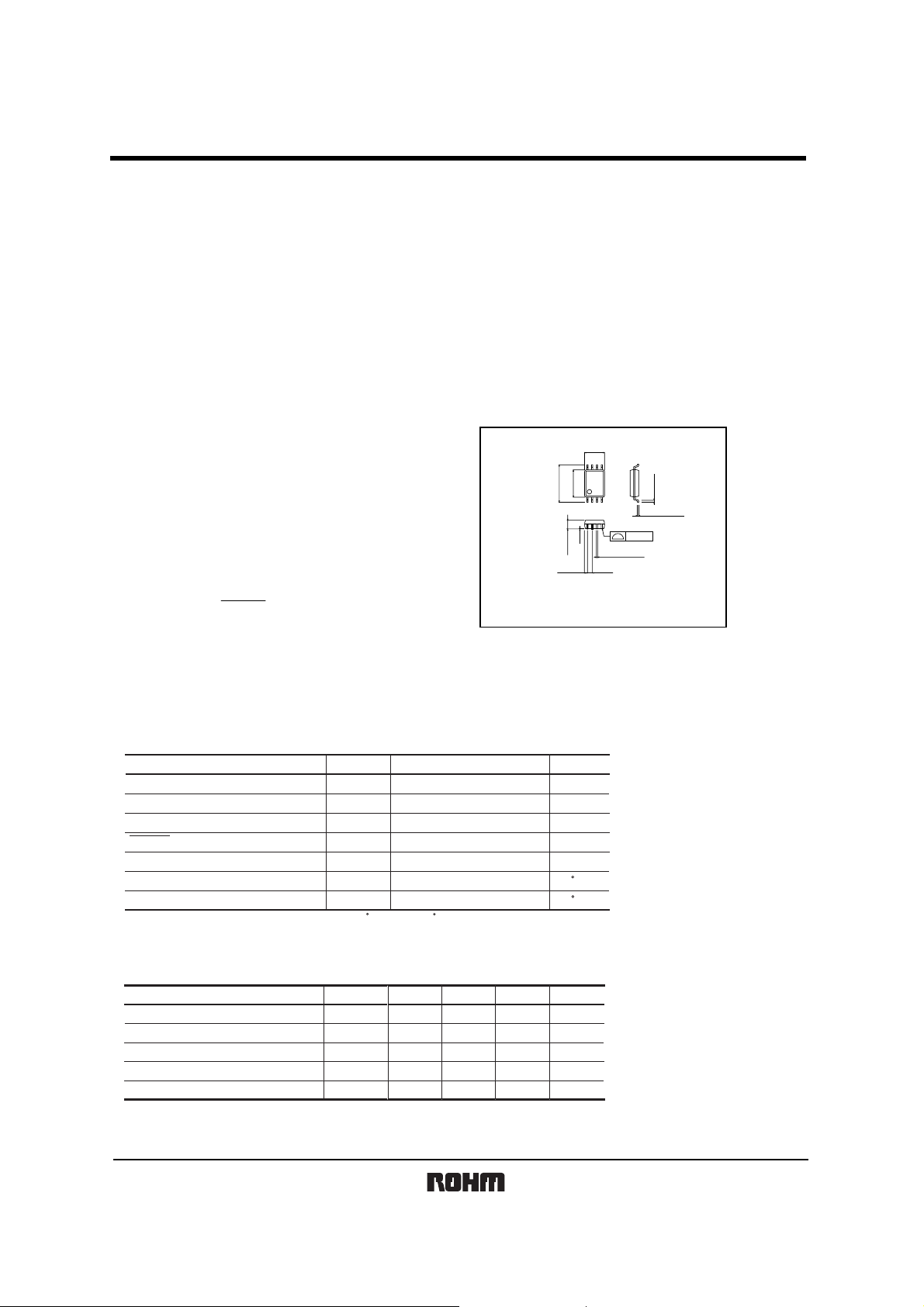
zExternal dimensions (Unit : mm)
3.0±0.2
0.2
±
4.4
6.4±0.3
1
0.1
1.15±0.1
(0.52)
SSOP-B8
Unit
V
V
15
15
∗
350
−30 to +85
−40 to +125
-
-
-
-
-
V
V
mW
C
C
mA
mA
mA
548
0.3Min.
0.15±0.1
0.1
0.22±0.1
0.65
1/8
Page 2
Regulators
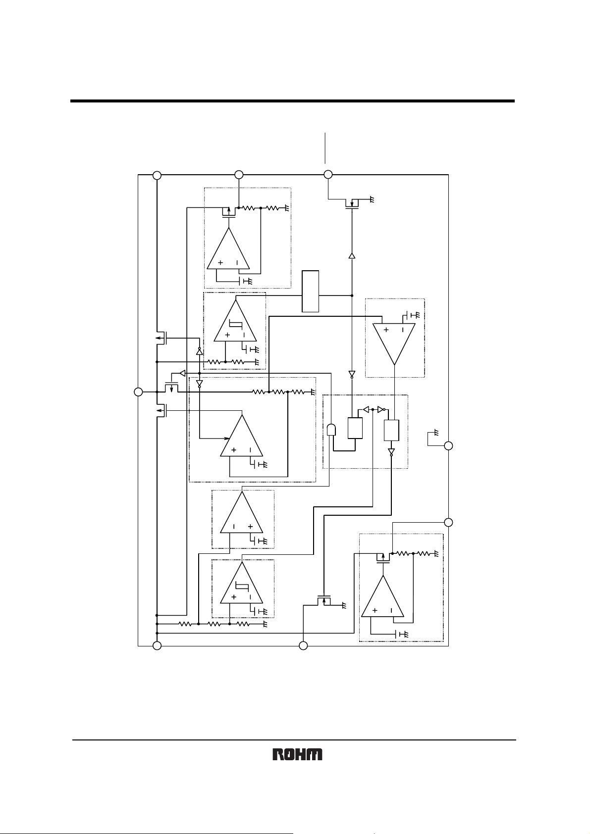
zBlock diagram
BD4201FV
Vout
Vbat
M1
Vch
REG3
RESET Voltage detector
DELAY
RESET
R
Q
Vsw2 Detection circuit
S
S
R
Q
Vss
REG2
Switch control circuit
Vro
Vsw1 Detection
circuit
CS Voltage
detection
Vin
CS
Fig. 1
2/8
REG1
Page 3
Regulators
zCircuit around pin
BD4201FV
Pin No. Pin Name
1
3 4
5
Vss
Vbat
Vbat
RESET
RESET
RESET voltage detector
output Pin
Function
Ground Pin
Vss
Back up power supply
input Pin
Pin No. Pin Name Function
2
6
Vch
Vch
CS
CS
Vout
Regulator 3 output Pin
Vin
CS voltage detector output Pin
Regulator2 output Pin
Vin
Vbat
Vout
7
Vin
Main power supply input Pin Regulator1 output Pin
Vin
8
3/8
Vro
Vro
Vin
Vin
Page 4

Regulators
zElectrical characteristics (Unless otherwise specified Vin=6V, Ta=25°C)
Parameter
Symbol Min. Typ.
[General spec]
Main circuit current1
Backup circuit current1
Backup circuit current2
lin1
lbat1
lbat2
[Regulator1]
Output voltage 1
Dropout voltage 1
Load regulation 1
Linc regulation 1
Vro
Vdif1
Vlo1
Vli1
2.93
[Regulator2]
Output voltage 2
Dropout voltage 2
Load regulation 2
Linc regulation 2
[Regulator3]
Output voltage 3
Dropout voltage 3
Load regulation 3
Linc regulation 3
[Voltage detect block]
CS detect voltatge
CS release voltage
RESET detect voltage
RESET release voltage
RESET release delay time
Low operating voltage
CS sink current
CS leak current
RESET sink current
RESET leak curent
[Switch control block]
Switch voltage
CS no output voltage
Vbat switch leak current
Vbat switch resistor
This product is not designed for protection against radioactive rays.
Vout
Vdif2
Vlo2
Vli2
Vch
Vdif3
Vlo3
Vli3
−Vdet1
+Vdet1
−Vdet2
+Vdet2
+Tdet2
Vopr
lcss
lcst
lres
lrel
Vsw1
Vsw2
IIek
Rsw
2.93
3.32
3.235
3.320
2.156
2.232
2.822
2.79
−
−
−
−
−
−
−
−
−
−
−
−
200
2.0
250
−
150
−
−
10
0.0
1.5
3.00
0.1
30
50
3.00
0.25
30
60
3.30
0.1
30
50
3.300
3.400
2.200
2.312
300
500
300
2.89
2.85
30
Max. Units Conditions
15
0.5
2.1
3.07
0.35
100
100
3.07
0.35
110
110
3.38
0.35
110
110
3.365
3.480
2.244
2.391
−−
−
−
−
−−
0.1
−
0.1
2.958
2.91
1
60
µA
µA
µA
V
V
mV
mV
V
V
mV
mV
V
V
mV
mV
V
V
V
V
µS
V
µA
µA
µA
µA
V
V
µA
Ω
BD4201FV
Vin=3.6V No load
Vin=3.6V Vbat=3V No load
Vin : Open Vbat=3V No load
Vin=7.2V, lro=3mA
lro=3mA
Vin=7.2V, lro=100µA∼20mA
Vin=4∼10V, lro=3mA
Vin=7.2V, lout=23mA
lout=23mA
Vin=7.2V, lout=100µA∼60mA
Vin=4∼10V, lout=23mA
Vin=7.2V, lch=3mA
lch=3mA
Vin=7.2, Ich=100µA∼20mA
Vin=4∼10V, lch=3mA
Vin voltage detection
Vout voltage detection
Vin or Vbat
Vcs=0.5V, Vin=Vbat=2.0V
Vcs=15V, Vin=15V
Vreset=0.5V, Vin=Vbat=2.0V
Vreset=15V, Vin=15V
Vbat=2.8V
Vbat=3V
Vin=3.6V, Vbat=0V
Vin=OPEN, Vbat=3V, Iout=10~500µA
4/8
Page 5

Regulators
zMeasurement circuit
BD4201FV
SW1
a
Ich
zApplic ation circuit
V
V1
b
SW2
Vss
1
2
Vch
10µF
Vbat
3
b
a
I2
A
SW3
b
V
a
A
I3
V2
4
CS
Fig.2
Vro
Vin
Vout
RESET
6
8
7
5
V3
A
10µF
V
I4
a
I1
A
10µF
SW6
a
SW4
SW7
V5
V
b
V4
V
a
Iout
b
a
SW5
b
Iro
b
d
c
A
I6
CS
Vch
Vout
100kΩ
10µF
3V
1
2
3
4
Vss
Vch
Vbat
CS
Vro
Vin
Vout
RESET
8
10µF
7
6V
6
22µF
5
0.01µF0.01µF
Vro
Vout
100kΩ
Fig.3
5/8
RESET
Page 6

BD4201FV
Regulators
zNote for use
1. The application circuit is r ecommended for use. M ake sure to confirm the a dequacy of the characterist ics. When
using the circuit with changes to the exter n al circu it co nstants, mak e sur e to leave an adeq u ate mar gi n for ext erna l
components including static and transitional characteristics as well as dispersion of the IC.
2. Operation supply voltage range
The circuit functionality is guarant eed within th e operation of amb ient temperat ure range, as lo ng as it is within the
operation supply voltage range. T he standard of electric al characteristic values cannot be guaranteed at other
voltages in the operating range, however , the variation will be small.
3. The regulator output circuit of this IC does not include protect circuit for the unusual situations such as over voltage
current protection, short detect circuit and thermal shut-down circuit.
Therefore, this IC might be broken down when it is loaded exceeding the package pow er , or when it is shorted.
T o design application circuit, please deal it w ith enough consideration.
4. Oscillation stopper of output and byp ass capacitor
Please put into capacitor to stop oscillation between output pin and GND.
It has a possibility of oscillation if ca pacit ance is changed due to temp erature range , and it recomme nds to use small
tantalum electrolytic capacitor of equivalents serial resistor (ESR).
If extremely big capacitor is used, it may have a case to occur oscillation of low frequency.
Please confirm this point. And it recommend to put into byp ass cap a citor in to the neares t position betw een inpu t pin
and GND.
5. For the grounding shown in the application circuit, w ire every ground to GND terminal in a short p attern arrangement to avoid electrical disturbance.
6. This product is produced with stri ct quality control, but might be destroyed in using bey ond absolute maximum
ratings is considered. Open IC destroyed a failure mode cannot be defined (I like short mode, or open mode).
Therefore, physical security countermeasure, like fuse, is to be given when a specific mode to be beyond absolute
maximum ratings is considered.
7. Mal-function may happen w hen the device is used in the strong electromagnetic field.
8. Recommended to put DIODE for protection purpose in case of output pin connected w ith large load of inpedance
or reserve current occurred at initial and output off.
(Example)
OUTPUT PIN
This IC is monolithic IC which (as shown in Figure-4) has P+ isolation in the P substrate and betw een the various
9.
pins. A P-N junction is formed from this P layer and N lay er of each pin. For example, the relation between each
potentials is as follows;
(When GND > pinB and GND > pinA, the P-N junction operates as parasitic diode.)
(When > pinB > GND > pinA, the P-N junction operates as parasitic transistor.)
Parasitic diodes can occur inevitably in the structure of the IC. The operation of parasitic diodes can result in mutual
interference among circuits as well as operation faults and physical damage.
Accordingly, Please do not use methods by which p arasitic diode operate, such as applying a volt age that is lower
than the GND (P substrate) voltage to an input pin.
6/8
Page 7

Regulators
Transistor (NPN)
Resistance
(Pin A)
~
~
+
NN
P substrate
P
N
PP
(Pin B)
NN
C
P
B
E
N
N
P substrate
~
~
P
BD4201FV
+
P
GND
(Pin A)
zPin layout
GND
Parasitic diode
~
~
parasitic diode
Fig.4 Simplified structure of IC
(Pin B)
Parasitic diode
or transistor
B
~
~
C
GND
Parasitic diode
or transistor
Vss
Vch
Vbat
CS
1
2
3
4 5
Fig. 5
7/8
8
7
6
Vro
Vin
Vout
RESET
Page 8

Regulators
Power dissipation
zElectrical characteristic curves
(mW)
500
400
300
200
100
25
50 75 100 125 150
Temperature
BD4201FV
( C)
Fig.6 Power dissipation curve
8/8
 Loading...