Page 1

DDR-SDRAM Termination Regulator
BD3531F
●Description
BD3531F is a regulator developed as termination
power supply of standard DDR-SDRAM that is
used for PC.
Industry's highest speed of transient response
characteristic is realized. The built-in FET can sink
and source load current of 1.5A(max.)
Waveform quality when data is transferred at high
speed can't be deteriorated.
BD3531F meets the bus line standards SSTL-2 of
DDR-SDRAM.
High-reliability can be realized for any applications
using DDR-SDRAM.
●Features
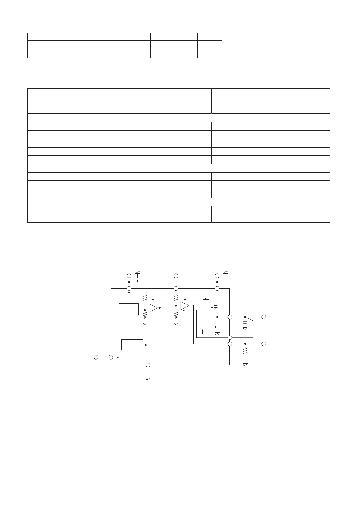
1) Built-in push-pull regulator for termination(VTT)
2) Built-in reference voltage circuit(VREF)
3) Built-in enable function
4) Built-in under voltage lock out circuit
5) Package SOP8
6) Built-in thermal shut down circuit
●Applications
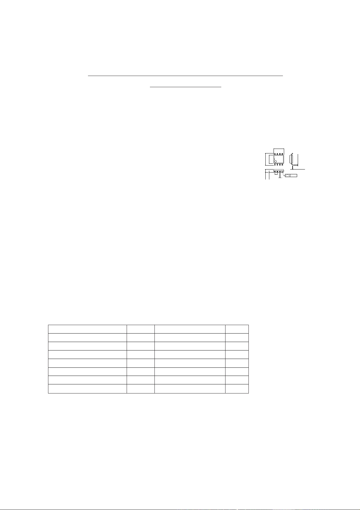
●Dimension (Unit : mm)
6.2±0.3
1.5±0.1
5.0±0.2
8 5
4.4±0.2
1.27
0.11
0.4±0.1
SOP8
0.3Min.
41
0.15±0.1
0.1
Note personal computer, Desktop personal computer
●Absolute Maximum Ratings(Ta=25˚C)
Parameter Symbol
Input voltage
Termination input voltage
VDDQ reference voltage
Power dissipation 1
Power dissipation 2
Operating temperature range
Storage temperature range
*1 Should not exceed Pd.
*2 Reduced by 4.48mW for each increase in Ta of 1˚C over 25˚C(With no heat sink).
*3 Reduced by 5.52mW for each increase in Ta of 1˚C over 25˚C(PCB(70mm×70mm×1.6mm)glass epoxy mounting.)
VCC
VTT_IN
VDDQ
Pd1
Pd 2
Topr
Tstg
Limits
*1
7
*1
7
*1
7
*2
560
*3
690
+
〜
〜
+
100
150
-
10
-
55
Unit
V
V
V
mW
mW
˚C
˚C
Page 2

●Recommended Operating Conditions(Ta=25˚C)
Parameter Min. Max. UnitTyp.Symbol
Input voltage VCC
Termination input voltage VTT_IN
*This product is designed for protection against radioactive rays.
4.5 5.5 V
1.7 2.6 V
●Electrical characteristics (Unless otherwise noted, Ta=25˚C, VCC=5V, VEN=3V, VDDQ=2.5V, VTT_IN=2.5V)
Symbol Min. Max. Unit ConditionsTyp.Parameter
Standby current IST
Bias current
ICC
<Termination>
Termination voltage
Source current
Sink current
Upper side ON resistance
Lower side ON resistance
VTT
ITT+
ITT
-
HRON
LRON
<Reference voltage>
Output voltage
Source current
Sink current
VREF
IREF+
-
<UVLO>
UVLO OFF voltage
Hysteresis voltage
*Design Guarantee
-
-
-
-
0.8
2
VREF-30mV VREF+30mVVREF
1.5
-
-
-
1/2×
VDDQ-50mV
-
-
0.4
0.4
1/2×
VDDQ
10 20
- -
20
4.2 4.35 4.5VUVLO
100 160 220ΔVUVLO
1.6
4
-
-
1.5
0.8
0.8
1/2×
VDDQ+50mV
-
-
10IREF
VEN=0V
mA
mA
Io=-3A to 3A, Ta=0℃ to 100℃
V
A
A
Ω
Ω
IREF=-10mA to 10mA
V
Ta=0℃ to 100℃
mA
mA
VCC : Sweep up
V
VCC : Sweep down
mV
*
*
●Application Circuit
V
C
C
V
C
C
VC
R
ef
er
ence
B
ock
l
Therm
P
r
ot
E
E
n
a
b
N
e
l
-
+
al
TS
ect
D
i
on
GND
V
D
DQ
V
D
DQ
C
U
V
LO
VC
5
0
5
0
C
kΩ
U
V
kΩ
LO
V
T
T
_
I
N
V
T
T
_
I
N
VC
C
Li
n
er
N
-
M
O
S
D
r
ver
i
TS
D
E
N
U
V
LO
BD3531F
V
T
T
V
T
T
S
V
R
E
F
V
T
T
1
/2
×
V
D
DQ
 Loading...