

Page 1

BA6283N / BA6955N
Motor driver ICs
Reversible motor driver
BA6283N / BA6955N
The BA6283N and BA6955N are reversible-motor drivers with a maximum output current of 1.0A. Two logic inputs allow
four output modes: forward, reverse, stop (standby), and brake.
The built-in power save circuit suppresses current consumption in the motor stop mode.
!!!!Applications
VCRs, audio devices
!!!!
Features
1) Logic and driver sections have separate ground pins; this allows the IC to drive speed-variable, reversible motors by
connecting an electronic governor circuit.
2) Built-in power saving circuit suppresses current consumption in stop (standby) mode.
3) Interfaces with TTL devices.
4) Built-in thermal shutdown circuit.
!!!!
Absolute maximum ratings
Parameter Symbol Limits Unit
Applied voltage
Power dissipation Pd
Operating temperature Topr
Storage temperature Tstg
Output current
∗1 Reduced by 9.2mW for each increase in Ta of 1°C over 25°C.
∗2 Reduced by 8.64mW for each increase in Ta of 1°C over 25°C.
∗3 Should not exceed Pd or ASO values.
BA6283N
BA6955N
(Ta = 25°C)
V
CC
I
OUT
!!!!Recommended operating conditions (Ta = 25°C)
Parameter
Operating power supply voltage
Symbol Min. Typ. Max. Unit
CC
V
M
V
5.5 15 V
5.5 15 V
18 V
∗1
1150
∗2
1080
−20~+75
−55~+150
∗3
1000
−
−
mW
°C
°C
mA
Page 2
Motor driver ICs
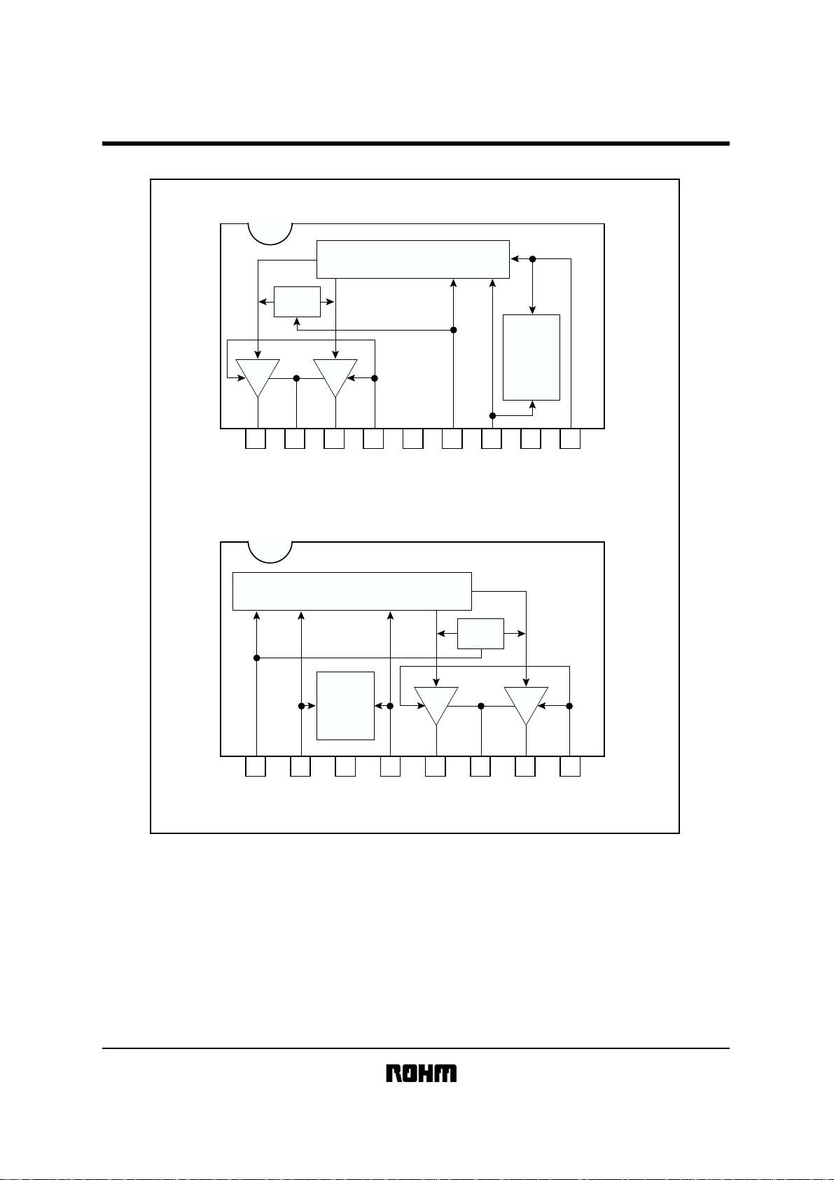
!!!!Block diagram
BA6283N
BA6955N
CONTROL LOGIC
TSD
POWER
SAVE
1 2 3 4 5 6 7 8 9
OUT2 OUT1 GND GNDR
NF
V
M
V
CC
F
IN
BA6283N / BA6955N
R
IN
CONTROL LOGIC
TSD
POWER
SAVE
1 2 3 4 5 6 7 8
V
CC
F
IN
R
IN
OUT2 OUT1GND R
NF
V
M
Page 3
Motor driver ICs
!!!!Pin descriptions
BA6283N
Pin No. Functions
BA6955N
Pin No.
Pin name
1
2
3
4
5
6
7
8
9
1
2
3
4
5
6
7
8
OUT2
R
NF
OUT1
V
M
GND
CC
V
IN
F
GND
R
IN
Pin name
V
CC
IN
F
GND
R
IN
OUT2
R
NF
OUT1
V
M
Motor output
Output GND, for connecting resistor for output current detection
Motor output
Motor power supply
GND
Power supply
Logic input
GND
Logic input
Functions
Power supply
Logic input
GND
Logic input
Motor output
Output GND, for connecting resistor for output current detection
Motor output
Motor power supply
BA6283N / BA6955N
!!!!Input / Output circuit
OUT2
V
Fig.1
M
OUT1
R
NF
F
IN
R
IN
12k
4.7k
20k
GND
11k
11k
10k
Resistances are typical values
Fig.2
V
CC
Page 4

Motor driver ICs
!!!!Electrical characteristics (unless otherwise noted, Ta=25°C, VCC=9V, and VM=9V)
Parameter
Circuit current1
Circuit current2
Circuit current3
Input high level voltage
Input low level voltage
Input high level current
Output saturation voltage
Not designed for radiation resistance.
!!!!Measuring circuits
I
CC
Symbol
I
CC
1
I
CC
2
CC
3
I
IH
V
V
IL
I
IH
V
CE
Min.
−
−
−
2.0
−
50
−
Typ.
1.0
30
40
−
−
−
90
Max. Unit
43.5
58
15
0.8
130
1.5
mA
mA
µA
−
V
V
µA
V
Forward or reverse mode
Brake mode
Standby mode
V
IN
=2.0V
O
=200mA
I
Sum of the high and low side output
transistor voltages
∗Refer to the Input/Output truth table about the output mode.
Circuit current : I
CC
BA6283N / BA6955N
Conditions
−
−
V
CC
V
IF
V
IR
V
M
Fig.3
Input high level voltage, Input low level voltage
IF
, V
: V
I
IH
I
IH
IR
∗Refer to the Input/Output truth table about the output mode.
Input high level current
IH
at VIF=2V, IIH at VIR=2V
V
CC
A
V
IF
A
V
M
V
V
V
IR
: I
Fig.4
Page 5

BA6283N / BA6955N
Motor driver ICs
CE
: Sum of the high and low side output transistor voltage.
V
I
O
flows from High to Low Level output pins.
V
CC
V
IF
!!!!Circuit operations
(1) Input section (F
Control signals are input from these pins. Input circuit can be controlled with TTL or over voltage input.
Operation in each mode is show below.
Output current flows from OUT1 to OUT2 (forward mode) when F
(reverse mode) when R
the high-side output transistor is turned off to shut down the motor driving current and the low-side output transistor is
turned on to absorb the counter-electromotive force of the motor. When F
OUT2 are left open and the motor stops. In this mode the power save circuit turn to active, and whole the IC circuit off
cause the circuit current to minimize.
Input / output truth table
F
IN
H
L
H
L
V
IR
V V
V
OR
Fig.5
, RIN)
IN
is Low and RIN is High. Putting FIN and RIN both High result in the brake mode. In this mode,
IN
IN
R
OUT1
L
H
H
L
H
L
L
OPEN
V
OF
OUT2
L
H
L
OPEN
V
M
is High and RIN is Low, and from OUT2 to OUT1
IN
and RIN are both Low, both OUT1 and
IN
Mode
Forward
Reverse
Brake
Standby
(2) Output section (OUT1, OUT2)
Two logic inputs control the motor by changing the status of the bridge-configured transistors.
(3) Power supply section (VCC, VM)
V
is a logic Power supply terminal, and VM is a Motor Power supply terminal.
CC
(4) Thermal shut down (TSD)
When the IC internal temperature rises by the accident motor locked, the thermal shut down circuit is activated and all
the outputs turn off with regardless of input mode. Then, the temperature fulls and the thermal shut down circuit is
disactirated, the output returns with regard of the input mode.
This circuit is activated when the IC junction temperature rises above 175°C (Typ.) and disabled when it is 150°C
(Typ.).
(5) Power save circuit
When F
and RIN are both Low, all the IC circuit turns off and it decrease the IC consumption current.
IN
Page 6

Motor driver ICs
(6) Ground (GND, RNF)
Attached the current detection resistors at the R
attached the electronic governor, the speed-variable reversible motors can be constructed.
!!!!Application example
BA6238N
TSD
terminal, the current flowing in the motor can be detected. Also
NF
CONTROL LOGIC
POWER
SAVE
BA6283N / BA6955N
M
VCC
LOGIC
CONTROL IC
Fig.6
Page 7

Motor driver ICs
BA6955N
BA6283N / BA6955N
CONTROL LOGIC
TSD
POWER
SAVE
LOGIC
CONTROL IC
V
CC
Fig.7
M
!!!!Operation notes
(1) The quality of these products have been carefully checked; however, use of the products with applied voltages,
operating temperatures, or other parameters that exceed the absolute maximum rating given may result in the
damage of the IC and the product it is used in. If the IC is damaged, the short mode and open modes cannot be
specified, so if the IC is to be used in applications where parameters may exceed the absolute maximum ratings,
then be sure to incorporate fuses, or other physical safety measures.
(2) GND potential
The potential for GND pin must be kept lower than the potentials of the other pins regardless of the circumstances.
(3) Input pins
Voltage should never be supplied to the input pins when the V
voltage is not applied to the IC. Similarly, when V
CC
is applied, the voltage on each input pin should be less than VCC and within the guaranteed range for the electrical
characteristics.
CC
(4) Back-rush voltage
Depending on the ambient conditions, environment, or motor characteristics, the back-rush voltage may fluctuate.
Be sure to confirm that the back-rush voltage will not adversely affect the operation of the IC.
Page 8

BA6283N / BA6955N
Motor driver ICs
(5) Large current line
Large currents are carried by the motor power supply and motor ground for these ICs. Therefore, the layout of the
pattern of the PC board and the constants of certain parameters for external components, such as the capacitor
between the power supply and ground, may cause this large output current to flow back to the input pins, resulting in
output oscillation or other malfunctions. To prevent this, make sure that the PC board layout and external circuit
constants cause no problems with the characteristics of these ICs.
(6) Power dissipation
The power dissipation will fluctuate depending on the mounted conditions of the IC and the ambient environment.
Make sure to carefully check the thermal design of the application where these ICs will be used.
(7) Power consumption
The power consumption by the IC varies widely with the power supply voltage and the output current. Give full
consideration to the power dissipation ratting and the thermal resistance data and transient thermal resistance data,
to provide a thermal design so that none of the ratings for the IC are exceeded.
(8) ASO
Make sure that the output current and supply voltage do not exceed the ASO values.
(9) Precautions for input mode switching
To ensure reliability, it is recommended that the mode switching for the motor pass once through the open mode.
(10) Rush current
There are no circuits built into these ICs that prevent rush currents. Therefore, it is recommended to place a current
limiting resistor or other physical countermeasure.
(11) Factors regarding the thermal, power supply, and motor conditions. If the potential of the output pin sways greatly and
goes below the potential of ground, the operation of the IC may malfunction or be adversely affected. In such a case,
place a diode between the output and ground, or other countermeasure, to prevent this.
(12) Input pins (F
The F
and RIN) thermal characteristics
IN
and RIN pins have thermal characteristics. Take these thermal characteristics into consideration when using
IN
the IC.
(13) Thermal shutdown circuit (TSD)
When the junction temperature reaches approximately 170°C (Typ.) during operation, the driver outputs are all
turned off.
There is an approximate 20°C (Typ.) thermal hysteresis.
(14) Motor noise
To eliminate motor noise, connect a capacitor between OUT1 and GND and between OUT2 and GND. Alternatively,
connect a capacitor between OUT1 and OUT2, and also a diode between OUT1 and GND and between OUT2 and
GND (see the figure below).
OUT1
OUT2
OUT1
OUT2
Page 9

Motor driver ICs
BA6283N / BA6955N
!!!!Electrical characteristic curves
BA6283N
1000
BA6955N
500
POWER DISSIPATION : Pd (mw)
0
0507525 100 125 150
AMBIENT TEMPERATURE : Ta (°C)
Fig.8 Package thermal derating
characteristics
(V)
1.0
OL
Inputs
FIN : L RIN : H
0.8
Outputs : OUT1
VCC=9V
M=9V
V
0.6
0.4
0.2
OUTPUT HIGH VOLTAGE : V
0
OUTPUT CURRENT : IOL (A)
0.6 0.80.40.20 1.0
40
(mA)
CC
30
20
10
CIRCUIT CURRENT : I
0
0121648 20
Curcuit current 2
Inputs F
Curcuit current 1
Inputs F
SUPPLY VOLTAGE : VCC (V)
Fig.9 Circuit current vs.
power supply voltage
CC
V
IN
: H
R
IN
: H
IN
: H
R
IN
: L
(V)
CC
−0.5
V
OH
CC
−1.0
V
V
CC
−1.5
CC
−2.0
V
CC
−2.5
V
OUTPUT HIGH VOLTAGE : V
VCC−3.0
OUTPUT CURRENT : IOH (A)
Inputs
IN
: H RIN : L
F
Outputs : OUT1
VCC=9V
VM=9V
0.6 0.80.40.20 1.0
Fig.10 Output high level voltage vs.
output current
Fig.11 Output low level voltage vs.
output current
!!!!
External dimensions
BA6283N
5.8±0.2
1.2
10.5±0.5
3.5±0.5
(Units : mm)
21.8±0.2 2.8±0.2
1
2.54
SIP9
BA6955N
19.3±0.2
5.8±0.2
1.2
10.5±0.5
9
0.6
0.3±0.1
0.8
1.3
3.5±0.5
1
2.54
2.8±0.2
8
0.6
0.3±0.1
0.8
1.3
SIP8
 Loading...