

Page 1
Motor driver ICs
Reversible motor driver
BA6219B / BA6219BFP-Y
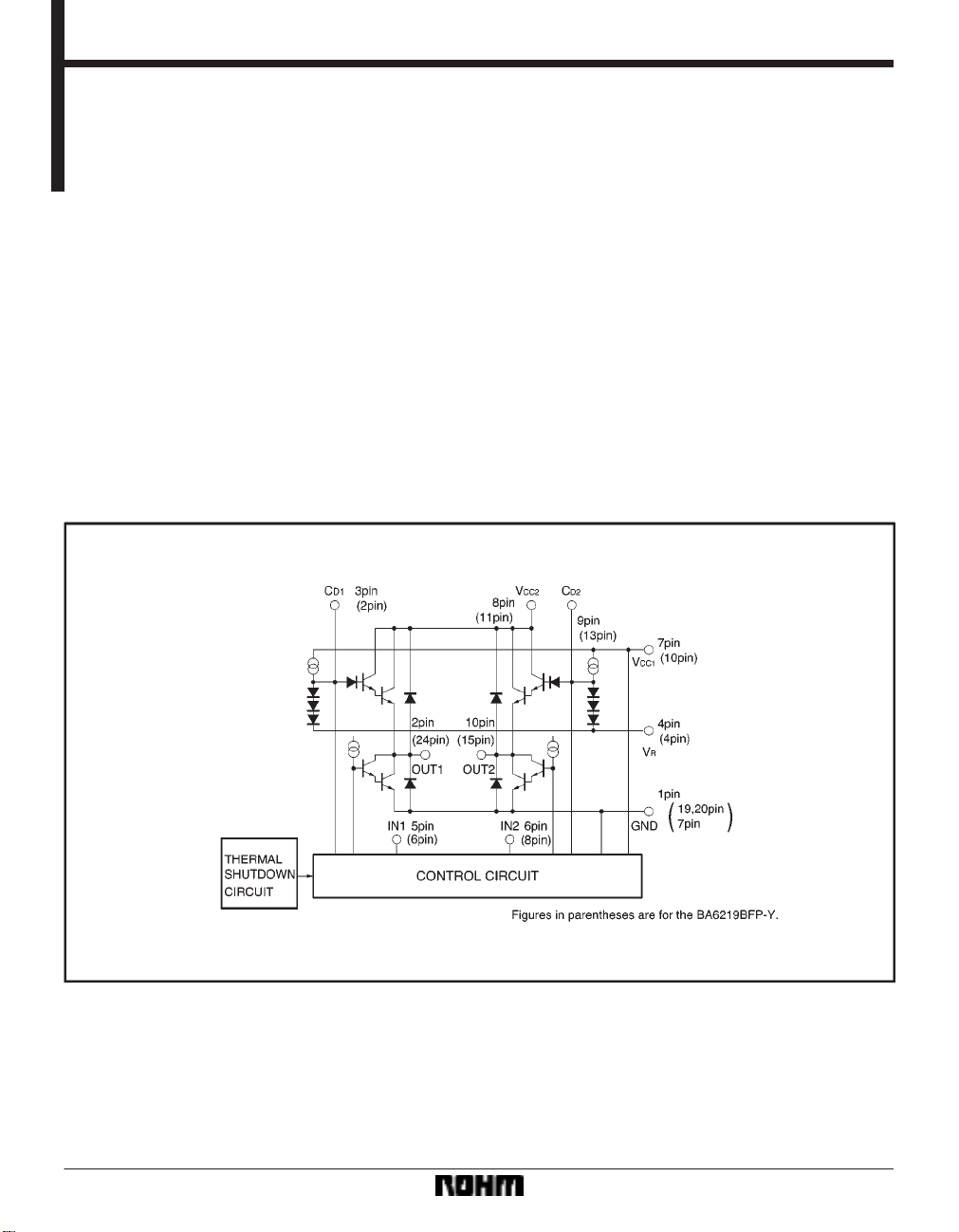
The BA6219B and BA6219BFP-Y are reversible-motor drivers suitable for brush motors. Two logic inputs allow four output modes: forward, reverse, idling, and braking. The motor revolving speed can be set arbitrarily by controlling the voltage applied to the motor.
Applications
VCRs and cassette tape recorders
Features
1) Large output current. (I
2) Built-in thermal shutdown circuit.
Block diagram
O=2.2A Max.)
3) Built-in output voltage setting pins.
4) Small standby supply current.
398
Page 2
Motor driver ICs BA6219B / BA6219BFP-Y
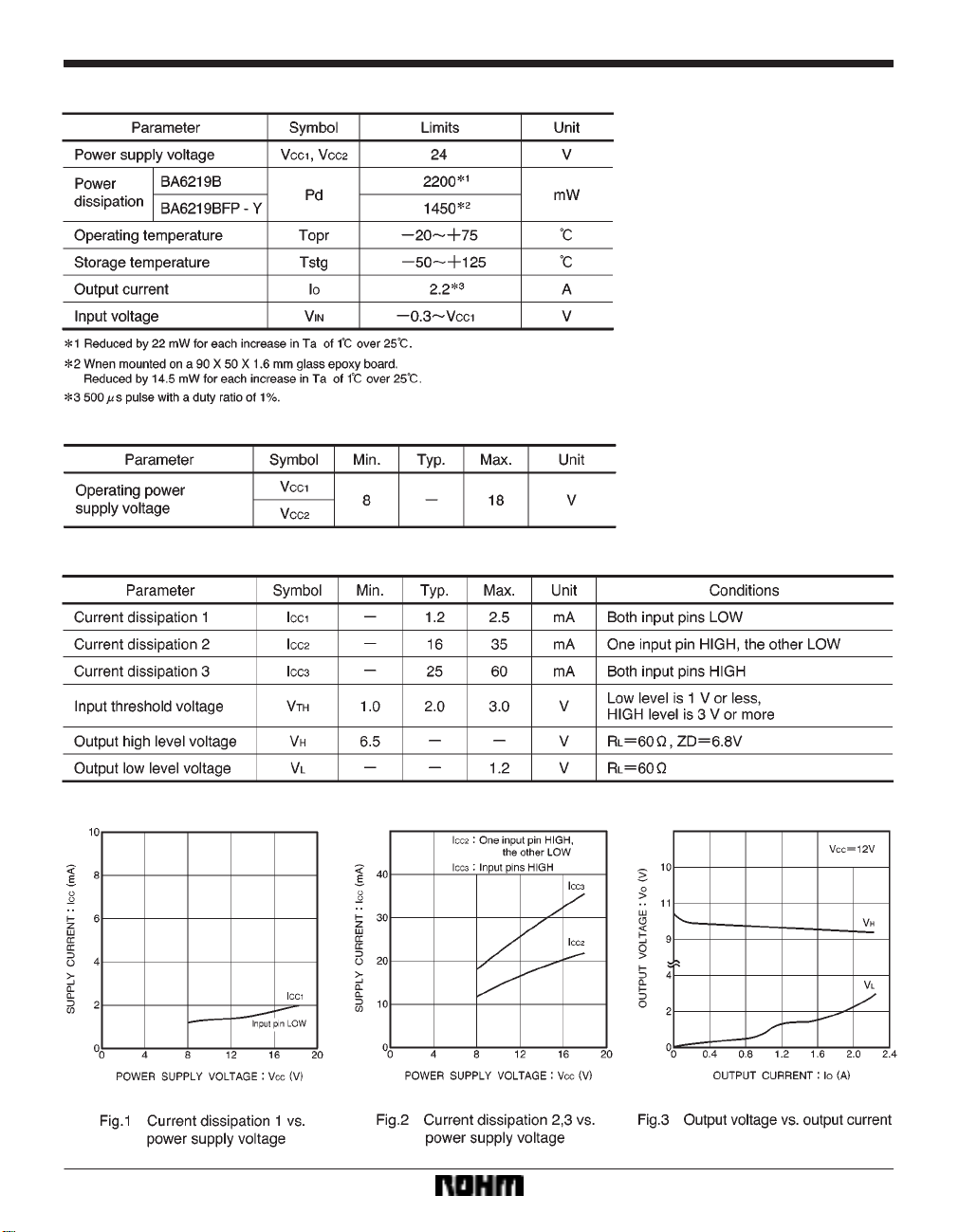
FAbsolute maximum ratings (Ta = 25_C)
FRecommended operating conditions (Ta = 25_C)
FElectrical characteristics (unless otherwise noted, Ta = 25_C and V
FElectrical characteristic curves
CC = 12V)
399
Page 3
Motor driver ICs BA6219B / BA6219BFP-Y
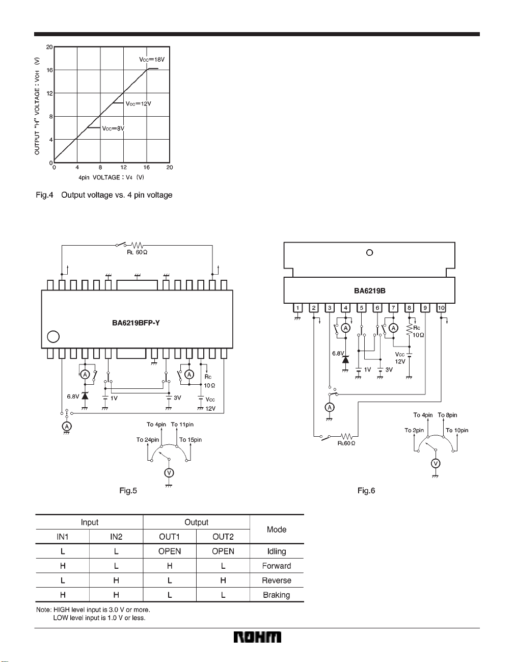
Measurement circuits
Input / output truth table
400
Page 4
Motor driver ICs BA6219B / BA6219BFP-Y
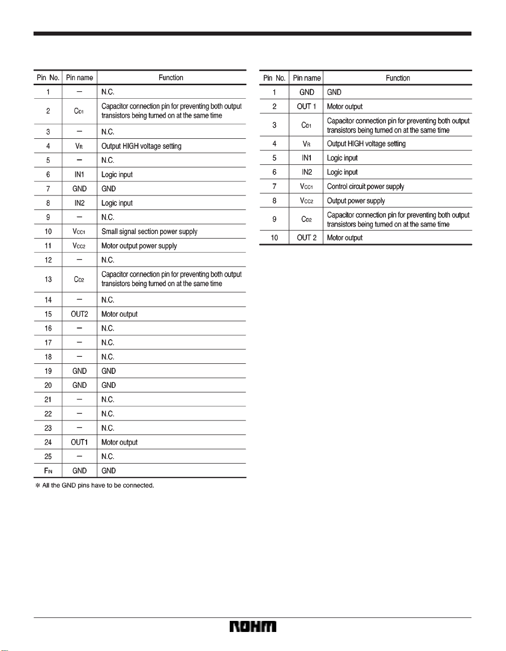
Pin descriptions
(BA6219BFP-Y) (BA6219B)
401
Page 5
Motor driver ICs BA6219B / BA6219BFP-Y
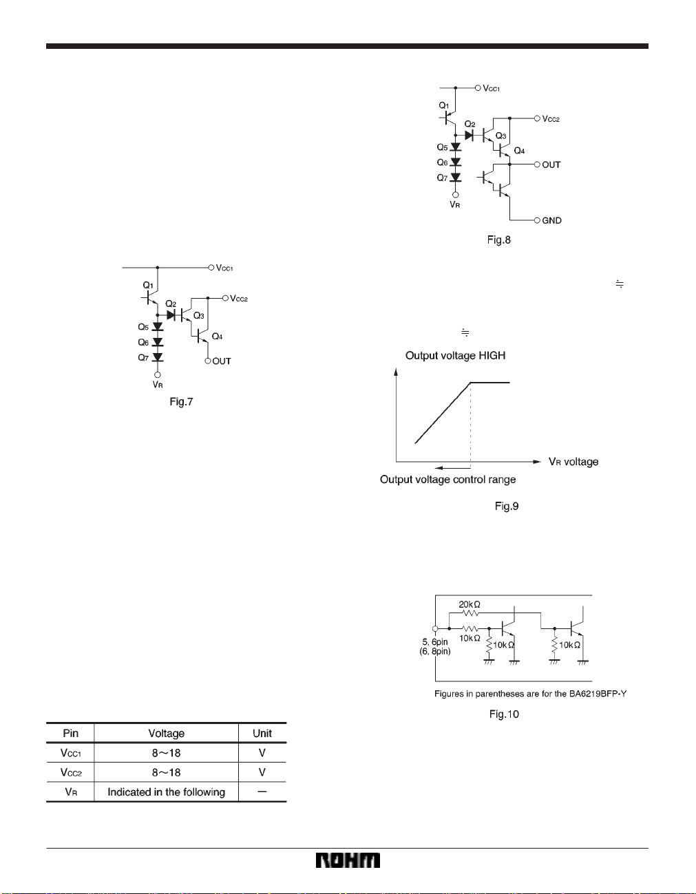
FOperation notes
(1) A schematic for the internal circuit associated with
the output voltage setting pin (Pin 4) is shown in Fig. 7.
The maximum output voltage (V
OMAX.=VCC1 VSAT (Q1) VBE (Q2) VBE (Q3) VBE (Q4)
V
For the condition of VR being equal to or less than
OMAX., the relationship between the output voltage (VO)
V
and the pin 4 voltage is given by :
V
O=VR {(VBE (Q5) VBE (Q6) VBE (Q7)) (VBE (Q2) VBE
(Q3) VBE (Q4))}
Though ∆V
nearly equal to V
BE depends on the output power supply, VO is
R.
(2) Thermal shutdown circuit
The thermal shutdown circuit turns off the driver output
if the chip temperature rises to about 180_. The shutdown signal is not latched.
(3) Power supply impedance
When the motor stops or starts, a rush current flows in the
VCC and GND lines. Depending on the way of connecting a power supply decoupling capacitor (100µF), the
control input voltage may become a negative value or the
supply voltage may drop to below the output voltage.
This can cause erratic operations due to parasitic effects.
Make sure that pin voltages will not exceed the supply
voltage by more than 0.3V or will not become less than
the GND pin voltage by more than 0.3V.
(4) VCC1, VCC2, and VR are related to each other as
shown in the output circuit diagram of Fig. 8. Their values
should be kept within the following ranges.
OMAX.) is given by :
(1) When the output voltage control pin (pin 4) is used
V
R < VCC1 (VSAT (Q1) VBE (Q5) VBE (Q6) VBE (Q7)) VCC1
2.5V
R < VCC2 {(VSAT (Q3) VBE (Q3) VBE (Q2)) (VBE (Q5)
V
V
BE (Q6) VBE (Q7))} VCC2 1V
(2) When the output voltage control pin (pin 4) is not
R is either short-circuited to VCC1 or left OPEN.
used, V
(5) Input circuit
Operating supply voltage ranges
402
Page 6

Motor driver ICs BA6219B / BA6219BFP-Y
(6) The quality of these products have been carefully
checked; however, use of the products with applied voltages, operating temperatures, or other parameters that
exceed the absolute maximum rating given may result in
the damage of the IC and the product it is used in. If the
IC is damaged, the short mode and open modes cannot
be specified, so if the IC is to be used in applications
where parameters may exceed the absolute maximum
ratings, then be sure to incorporate fuses, or other physical safety measures.
(7) Input pins
Voltage should never be applied to the input pins when
the V
CC voltage is not applied to the IC. Similarly, when
CC is applied, the voltage on each input pin should be
V
less than V
CC and within the guaranteed range for the
electrical characteristics.
(8) Back-rush voltage
Depending on the ambient conditions, environment, or
motor characteristics, the back-rush voltage may fluctuate. Be sure to confirm that the back-rush voltage will not
adversely affect the operation of the IC.
(9) Power dissipation
The power dissipation will fluctuate depending on the
mounting conditions of the IC and the ambient environment. Make sure to carefully check the thermal design of
the application where these ICs will be used.
(10) Power consumption
The power consumption by the IC varies widely with the
power supply voltage and the output current. Give full
consideration to the power dissipation rating and the
thermal resistance data and transient thermal resistance
data, to provide a thermal design so that none of the ratings for the IC are exceeded.
(11) ASO
Make sure that the output current and supply voltage do
not exceed the ASO values.
(12) Precautions for input mode switching
To ensure reliability, it is recommended that the mode
switching for the motor pass once through the open
mode.
(13) There are no circuits built into these ICs that prevent in-rush currents. Therefore, it is recommended to
place a current limiting resistor or other physical countermeasure.
(14) If the potential of the output pin sways greatly and
goes below the potential of ground, the operation of the
IC may malfunction or be adversely affected. In such a
case, place a diode between the output and ground, or
other measure, to prevent this.
403
Page 7

Motor driver ICs BA6219B / BA6219BFP-Y
Application examples
(1) BA6219B (2) BA6219BFP-Y
ZD : Zener diode to set output voltage. Use any zener
diode that is suitable for your application.
R
C : Resistor used for reducing collector loss and limit-
ing the short-circuit current. A resistance range of
310Ω is recommended.
C : Power supply filtering capacitor. Place as near as
possible to the V
CD : Capacitor to prevent both output transistors being
turned on at the same time.
CM : Capacitor to absorb surge voltage and prevent
parasitic oscillations.
CC1 pin.
External dimensions (Units: mm)
404
 Loading...