

Page 1
Regulator ICs
Trickle-charge IC for two-cell,
lithium-ion batteries
BA3170
The BA3170 is a trickle-charge IC developed for two-cell, lithium-ion batteries.The IC includes a charge control circuit,
a charge output transistor, and an LED driver for showing the charging status.
Applications
Lithium-ion (two cell) battery chargers, and charging circuits
Features
1) Output voltage can be varied using an external resistor.
2) The output pin is PNP output with low saturation voltage.
3) Built-in output current limiting circuit protects batteries from excessive current, and prevents destruction
of the IC due to output shorts.
The initial charge current is set to a low value (the current limit pin voltage can be used to vary the current
limit value).
4) Pulse charging at over 99% of the final voltage.
5) Built-in over-discharge battery return circuit.
6) Built-in charge fault protection circuit.
7) Built-in over-voltage battery operation circuit.
8) Built-in LED output for charge display (two outputs).
9) 12-pin power package provides large power dissipation in a compact package.
10) Temperature protection circuit prevents thermal destruction of the IC.
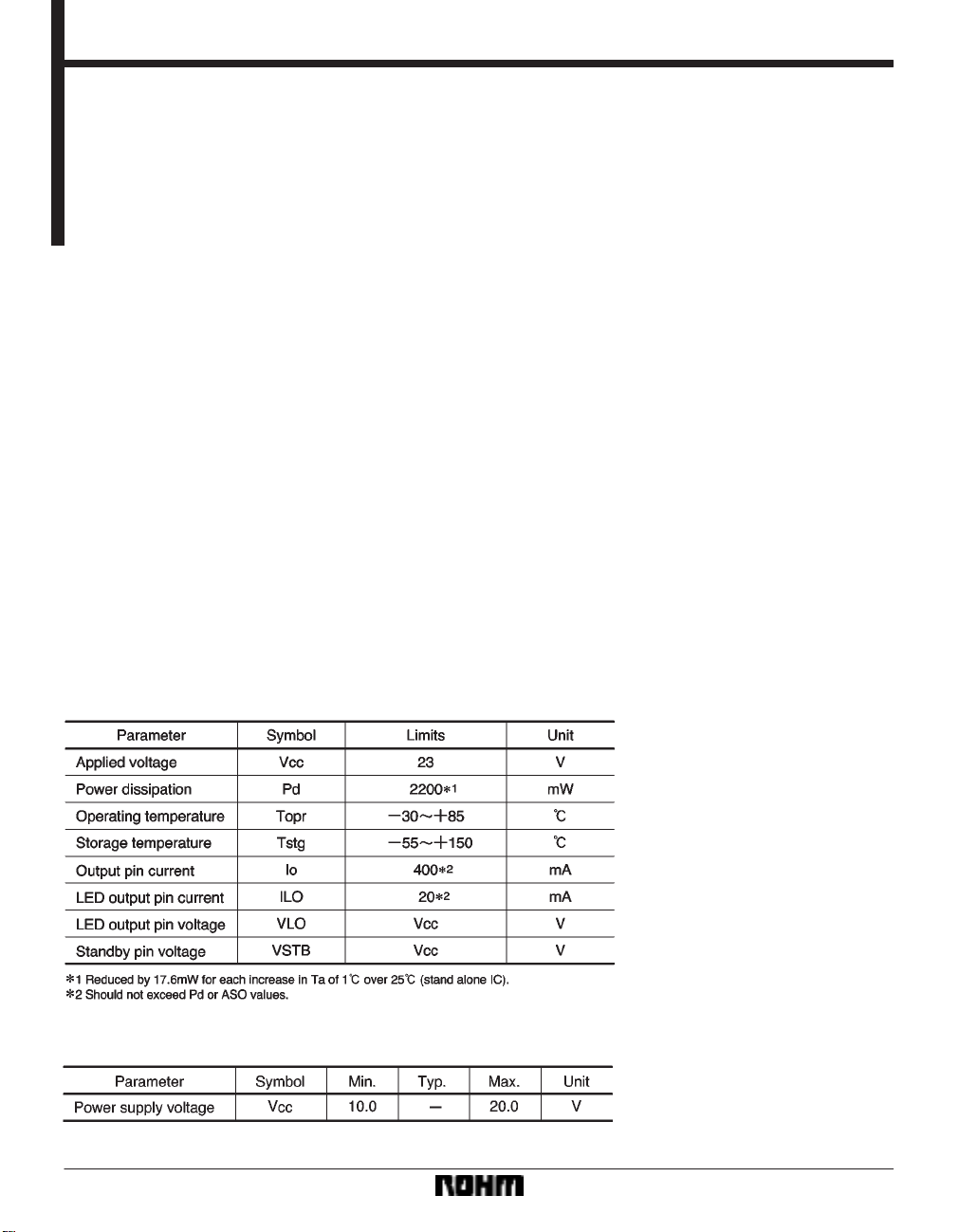
Absolute maximum ratings (Ta = 25C)
Recommended operating conditions (Ta = 25C)
395
Page 2
Regulator ICs BA3170
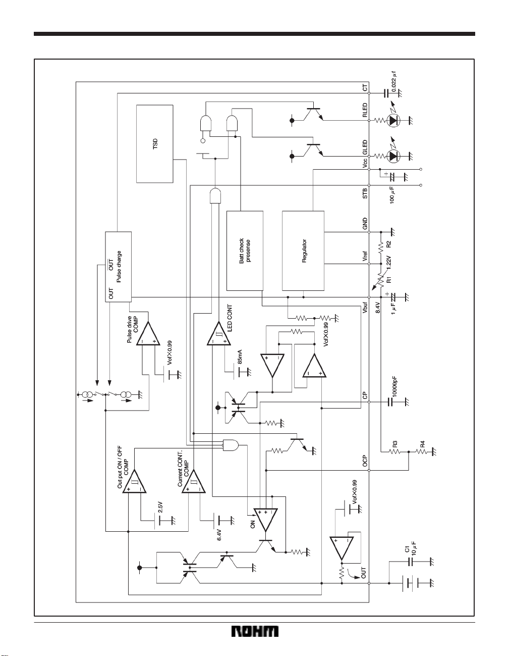
Block diagram
396
Page 3
Regulator ICs BA3170
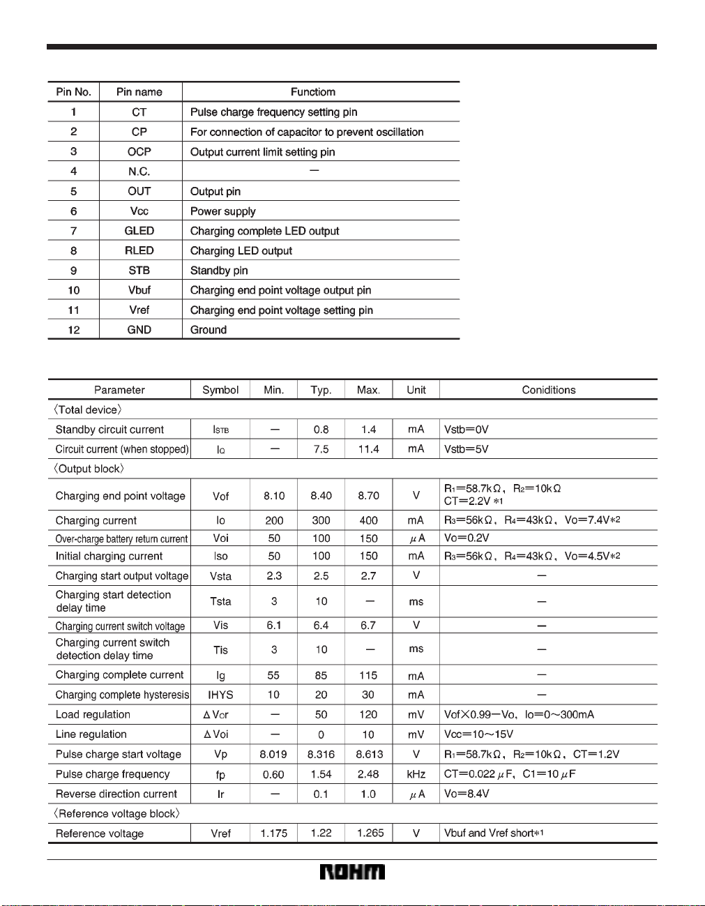
Pin descriptions
Electrical characteristics (unless otherwise noted, Ta = 25C, V
CC = 12V, R1 = 58.7kΩ, R2 = 10kΩ)
397
Page 4
Regulator ICs BA3170
Operation notes
(1) Do not use values other than CT = 0.022µF for the timing capacitor, and C1 = 10µF for the output capacitor.
(2) For the output capacitor C1, use a tantalum capacitor with low capacitance variation with temperature, and a static
capacitance tolerance of ±10% or less.
(3) For the timing capacitor CT, use a film capacitor with low capacitance variation with temperature, a static capacitance tolerance of ±10% or less, and a temperature variation rate of ±2% or less.
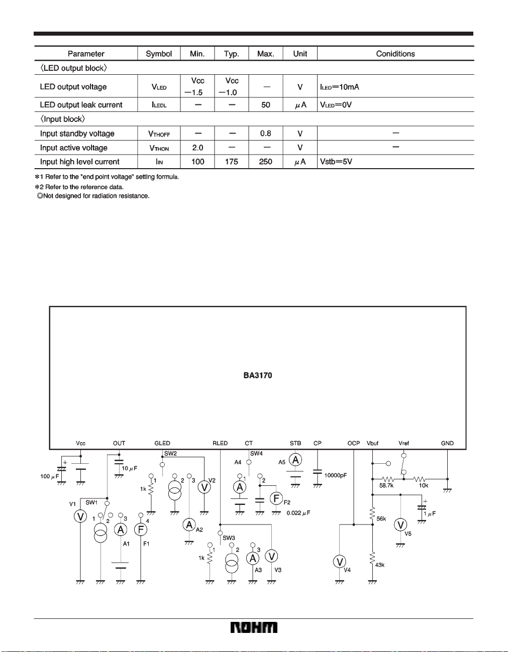
Measurement circuit
398
Fig.1
Page 5
Regulator ICs BA3170
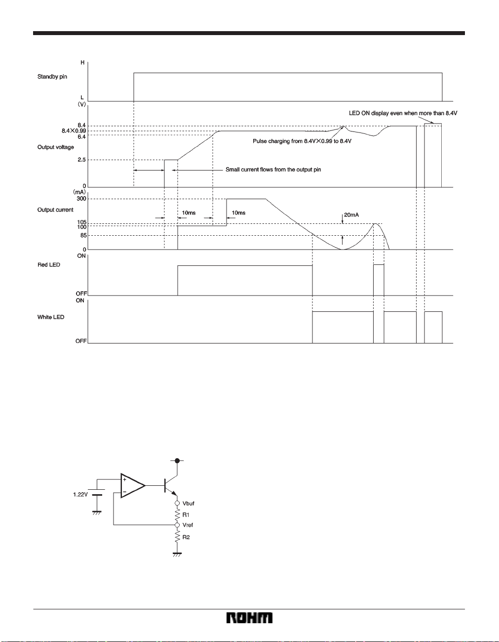
Timing chart
Fig.2
External components
Setting the “end point voltage” Set the “end point voltage” Vbuf using resistors R1 and
R2.
Example:
To set Vbuf to 8.4V:
1.22 = R2 / (R1 R2) 8.4
R1 = 5.88
. . .
R2
If R2 = 10kΩ, then
R1 = 58.7kΩ
∗ For measurement of the electrical characteristics, Vref and Vbuf are
shorted.
Fig.3
399
Page 6
Regulator ICs BA3170
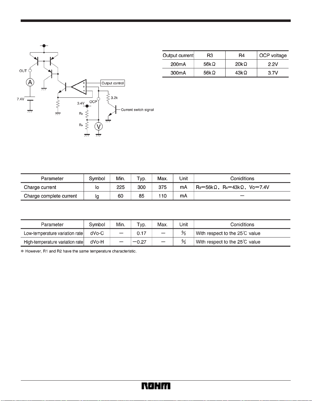
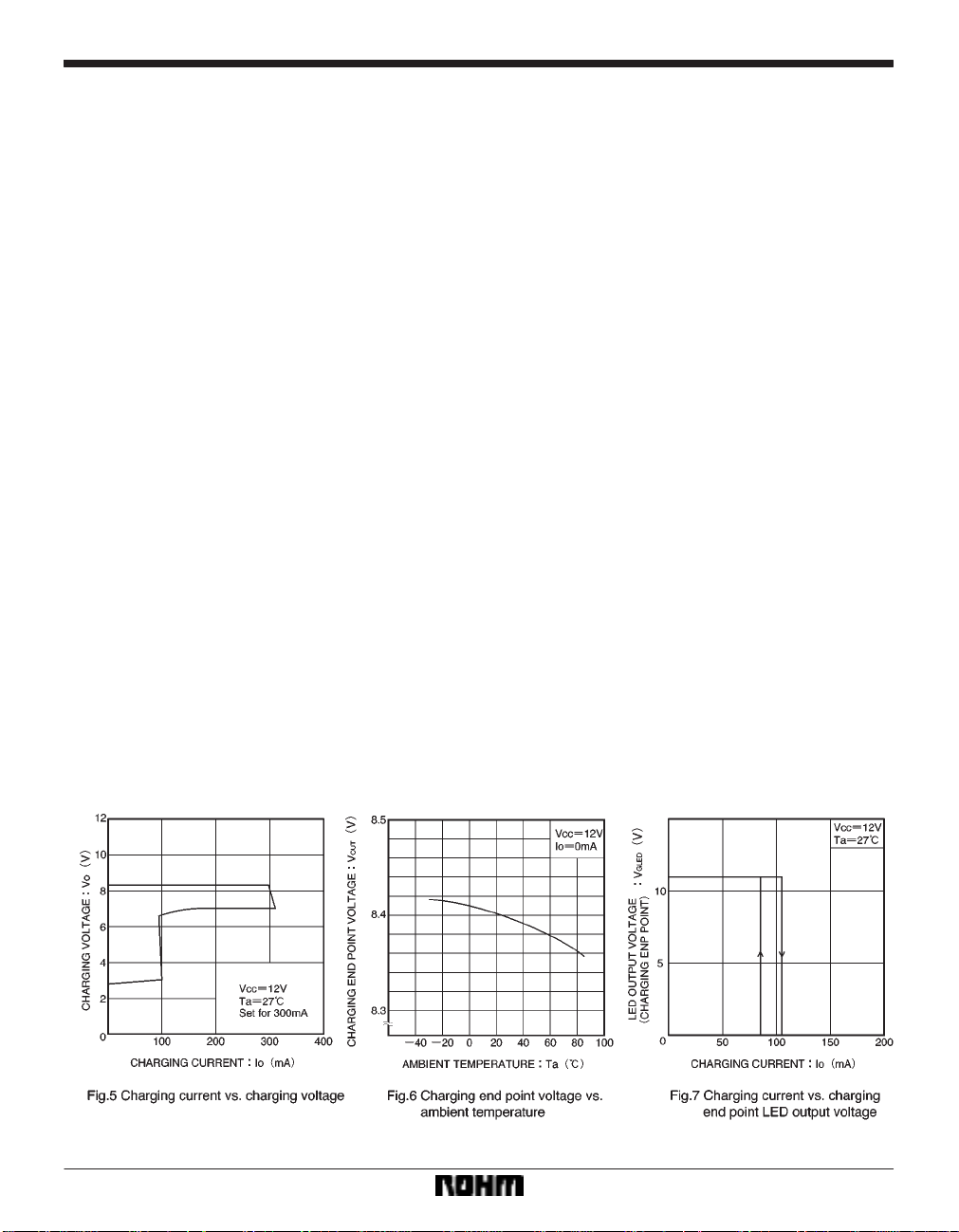
FReference data
S Output current limit value Set the value for the OCP voltage using R3 and R4(T a =
25_C, V
Fig.4
S Charging current and charge complete current for when the “end point voltage” is set to 8.4V ±50mV (Ta = 25_C and
V
CC = 12V)
CC = 12V, Vbuf = 8.4V, and Vo = 7.4V (Typ.))
S Charge “end point voltage” temperature characteristic (V
FOperation notes
(1) Application circuit (in the block diagram)
We guarantee the application circuit design, but recommend that you thoroughly check its characteristics in actual use.
If you change any of the external component values,
check both the static and transient characteristics of the
circuit, and allow sufficient margin in your selections to
take into account variations in the components and ICs.
Note that Rohm has not fully investigated patent rights
regarding this product.
400
CC = 12V, R1 = 58.7kΩ, R2 = 10kΩ, and CT = 2.2V)
(2) Operating voltage range
Provided that the IC is operated within the recommended
operating voltage range, the operation of the circuit is
guaranteed within the allowed operating temperature
range.
With regard to the values for the characteristics, the rating values for electrical characteristics cannot be guaranteed, but within these ranges there will not be a dramatic
change in the values for the characteristics.
(3) Notes regarding power dissipation (Pd)
A derating characteristic is provided for power dissipation. Your design should not require the component to
dissipate more than its maximum allowed power dissipation over the operating temperature range.
Page 7
Regulator ICs BA3170
(4) Over-voltage protection circuit
When the voltage between V
CC (pin 6) and GND (pin 12)
exceeds about 27V (at normal temperature), the overvoltage protection circuit switches all outputs off.
Make sure to use the IC within this voltage limit.
(5) Capacitors to prevent oscillation of the outputs
Be certain to connect capacitors between OUT (pin 5)
and ground, and CP (pin 2) and ground to prevent oscillation. We recommend tantalum capacitors that have low
capacitance variation with temperature (particularly for
the OUT pin).
(6) Thermal shutdown circuit
A thermal shutdown circuit is provided on the IC to prevent it from being destroyed by high temperatures. When
this circuit operates, all outputs go off, and when the temperature drops to a certain level, operation resumes.
(7) Output circuit construction
The outputs use PNP power transistors. When the V
(pin 6) voltage drops, even if the external capacitor on the
output side causes the output-side voltage to exceed the
CC-side voltage, the IC will not be destroyed.
V
(8) Grounding
With regard to the ground connections shown in the application example circuit, make the PCB connections
from each earth to the GND pin (pin 12) reasonably short,
and design your pattern layout to avoid electrical interference between the pattern lines.
(9) ASO
This IC includes a variety of protection circuits, but depending on the operation conditions, it may be possible
to exceed the ASO.
Exceeding the ASO will result in destruction of the IC, so
take due care to ensure that the ASO conditions are never exceeded.
(10) Great care has been paid to the quality of this component. However, due to the nature of lithium-ion batteries, if there is a risk of danger due to failure of this component (e.g. fire or explosion), be certain to take appropriate
measures in your design (fuses etc.).
CC
Electrical characteristics curves
401
Page 8

Regulator ICs BA3170
External dimensions (Units: mm)
402
 Loading...