

Page 1
BA3131FS
Standard ICs
Dual operational amplifier with switch,
for audio use (3 inputs × 1 output × 2)
BA3131FS
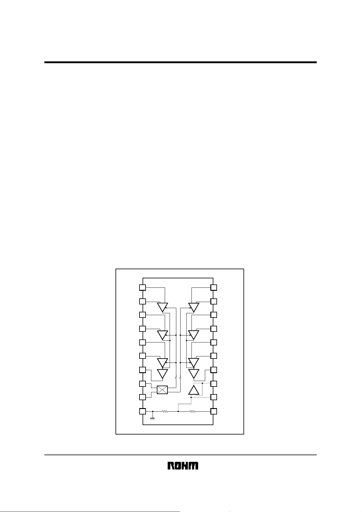
The BA3131FS contains two built-in circuits with operational amplifiers configured of three differential input circuits, an
output circuit, and a switch circuit. The three differential input circuits are separate, enabling independent settings to be
entered for the gain and frequency characteristics.
Applications
!
Car stereos, audio amplifiers and other electronic circuits
Features
!
1) High gain and low distortion. (Gv = 110dB, THD = 0.0015% typ.)
2) Low noise. (Vn = 2µVrms typ.)
3) Switching circuit can be directly coupled to microcomputer port.
4) Small switching noise.
5) Equipped with 1 / 2 Vcc output circuit for single power supply.
Block diagram
!!!!
+ IN1A
- IN1A
+ IN1B
- IN1B
+ IN1C
- IN1C
OUT1
SW1
SW2
GND
1
2
3
4
5
6
7
8
9
10
+
–
+
–
+
–
33
RR
+
–
+
–
+
–
+
–
20
19
18
17
16
15
14
13
12
11
+ IN2A
- IN2A
+ IN2B
- IN2B
+ IN2C
- IN2C
OUT2
Vref OUT
1 / 2 V
CC
V
CC
Page 2
BA3131FS
Standard ICs
Absolute maximum ratings
!!!!
Parameter Symbol Limits Unit
Power supply voltage V
Power dissipation 750
Operating temperature Topr ˚C
Storage temperature Tstg ˚C
Common-mode input voltage V
Differential input voltage V
Load current ± 50.0 mA
Reduced by 7.5mW for each increase in Ta of 1˚C over 25˚C.
∗
(When mounted on a glass epoxy board (90mm × 50mm × 1.6t))
Recommended operating conditions
!!!!
Parameter Symbol Min. Typ. Max. Unit Conditions
Operating power supply voltage
Electrical characteristics
!!!!
Parameter Symbol Min. Typ. Max. Unit Conditions
Quiescent current 2.0 4.9 7.8 mA
Input offset voltage - 0.5 5.0 mV
Input offset current - 5 200 nA
Input bias current - 50 500 nA
High-amplitude voltage gain 86 110 - dB
Common-mode input voltage 36-V
In-phase signal rejection ratio CMRR 60 72 - dB
Power supply voltage rejection ratio PSRR 76 90 - dB
Maximum output voltage /
Input conversion noise voltage - 2.0 4.0 µVrms
Reference voltage change - - ± 10 mV -
1 Because the first stage is contigured with PNP transistors, input bias current is from the IC.
∗
2 Tested under the following conditions: GV = 40dB, RS = 2kΩ, Matsushita Tsuko VP-9690A (using DIN audio filter)
∗
(Ta=25°C)
VCC
Pd
Vid
oMax.
I
Vi
18.0
∗
– 40 ~ + 85
– 55 ~ + 125
3 ~ VCC
VCC
mW
(Ta=25°C)
6.0 8.0 16.0 V single power source
CC
V
(unless otherwise noted, Ta=25°C, Vcc=8V)
Iq
Vio
Iio
Ib
Avol
Vicm
V
OH
36-V
V
Vn
∆V
36-V
OL
REF
VIN = 0, RL = ∞ , SW pin open
RS ≤ 10kΩ
1
∗
RL ≥ 2kΩ, V
O = ± 1.5V
RS ≤ 10kΩ
RS ≤ 10kΩ
RL ≥ 10kΩ
RL ≥ 2kΩ
2
∗
= ± 1mA
Ioref
Measurement
circuit
Fig.2
Fig.1
Fig.1
Fig.1
Fig.1
Fig.1
Fig.1
Fig.1
Fig.3
/
Fig.4
Fig.7
Design guaranteed values
!!!!
Parameter Symbol Min. Typ. Max. Unit Conditions
Slew rate SR 0.5 1.2 - V / µS
Gainbandwidth product GBW 1.5 2.6 - MHz f = 10kHz
Crosstalk between A, B and C CT
Total harmonic distortion
Channel separation
This item is not guaranteed during processes.
∗
(unless otherwise noted, Ta=25°C, Vcc=8V)
ABC
60 73 - dB f = 1kHz
THD - 0.0025 0.01 %
CS 90 115 - dB
V
= 0dB, RL = 2kΩ
G
GV = 0dB, f = 1kHz, VO = 1Vrms
f = 1kHz, input conversion
Measurement
circuit
Fig.5
Fig.6
Fig.8
Fig.9
Fig.10
Page 3
Standard ICs
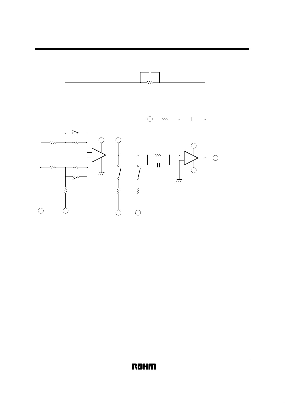
Measurement circuit
!!!!
C2
0.1µF
RK
50kΩ
BA3131FS
RK
RK
500kΩ
C3
1000pF
500kΩ
EK
S1
V
Rs
50Ω
Ri
10kΩ
CC
V
O
+
DUT
–
Rs
50Ω
50kΩ
VR
Ri
10kΩ
S2
Rf
Vref
RL1
2kΩ
S3
Vref
S4
RL2
10kΩ
Vref
C2 and C3 are used to prevent oscillation (adjustment required)
∗
–
NULL
+
C1
0.1µF
15V
VF
– 15V
Fig.1
Page 4

Standard ICs
Measurement conditions
!!!!
BA3131FS
(Figure 1)
5.5
2.5
VF
S1 S2 S3 S4
VF1
VF2
VF3
OFF ON
VF4
ON OFF
VF5
ON ON ON OFF 4
VF6
VF7
ON ON OFF OFF 5
VF8
VF9
ON ON OFF OFF 6
VF10
OFF OFF 3
Measurement Item EK Equation
Input offset voltage 8 — ON ON OFF OFF 1
Input offset current 8 — OFF OFF OFF OFF 2
Input bias current 8 —
High-amplitude voltage gain 8
Common-mode signal rejection ratio
(Common-mode input voltage)
Power supply voltage
rejection ratio
Equations
!!!!
V
CC
VR
Vref
Vref
Vref
Vref
868
820
Vref
6 —
Vref
18 —
(1) Input offset voltage (Vio)
Vio = | VF1 | / (1 + Rf / Rs)
(2) Input offset current (Iio)
Iio = | VF2 - VF1 | / (Ri (1 + Rf / Rs) )
(3) Input bias current (Ib)
Ib = | VF4 - VF3 | / (2 Ri (1 + Rf / Rs) )
(4) High-amplitude voltage gain (Avol)
Avol = 20log (3 (1 + Rf / Rs) / | VF6 - VF5 | ) (dB)
(5) In-phase signal rejection ratio (CMRR)
CMRR = 20log (4 (1 + Rf / Rs) / | VF8 - VF7 | ) (dB)
(6) (In-phase input voltage range) (PSRR)
PSRR = 20log (12 (1 + Rf / Rs) / | VF10 - VF9 | ) (dB)
Page 5

Standard ICs
Measurement circuits
!!!!
+
–
Vcc
BA3131FS
Iq
A
Vcc
+
–
1V
2k
or
10kΩ
VoH
V
Vref
Vref
Fig.2 Iq
1V
Vref
Vcc
+
–
Fig. 4 Maximum output voltage: Low
15
Vout (V)
5
SR = 10 /
t
t
Vref
2k
or
10kΩ
VoL
V
t (µsec)
Vref
Vref Vref
Fig. 3 Maximum output voltage: High
Vcc = 18V
–
V
IN
+
Fig. 5 Slew rate ( )
Vcc
–
+
10kΩ
GB = Vo / V
0.1µF
V
IN
f = 10kHz
Vref
V
OUT
RL
2kΩ
Vref
10µF
V
Vo
IN
× f
Fig. 6 Slew rate ( )
Fig. 7 Band width frequency gain
Page 6

Standard ICs
3.3µF
2.2kΩ 56kΩ
Vref
Vref
1k
47µF
+
–
100kΩ
Vcc
0.47µF
100kΩ
B.P.F
20Hz ~ 30kHz
Vn =
100 × 10
1 ÷
Von
1 × 10
BA3131FS
100k
Ω
–
~
Ω
100k
Ω
100k
1kΩ / 100k
Vref
V
f = 1kHz
Vref
A
+
Ω
–
B
+
Ω
–
C
+
IN
Ω
Channel selection
ABC
= 20log
CT
Vcc = 8V
Vo
VoA or VoB
VoC
1kΩ / 100k
1k
Ω
1kΩ / 100k
Von
3
3
Vref
1k
Ω
Vref
1k
Ω
Fig. 8 Input conversion noise voltage
Vref
Vcc
+
–
1kΩ
Vref
2.2kΩ
IN
V
f = 1kHz
3.3µF
56kΩ
~
Fig. 10 Total harmonic distortion
100kΩ
~
1kΩ
f = 1kHz
VrefVref
–
+
1k / 100kΩ
CS = 20log
Vcc = 8V
CH-2
0.47µF
100Vo2
Vo
Vo1
100kΩ
Vo = 1Vrms
Vo2
Distortion meter
Fig. 9 Crosstalk between A and B
100kΩ
–
+
1kΩ
1k / 100kΩ
VrefVref
CH-1
Fig. 11 Channel separation ( )
Vo1
Fig. 12 Channel separation ( )
Page 7

Standard ICs
Application example
!!!!
BA3131FS
IN2C
IN2B
IN2A
IN1A
IN1B
IN1C
3.3µ
3.3µ
10
Aamp: Gv = 20dB
Bamp: Gv = 10dB
Camp: Gv = 0dB
C7 C8 C9 C10
100µ 0.022µ 22µ 100µ
OUT2
Vcc = 8V
OUT1
R2
1k
47k
C6
3.3µ
C5
3.3µ
C4
20119218317416515614713812911
47k
1k
47k
1k
R16
10k
R14
3.3k
R12
R6
R10
R4
R8
BA3131FS
R13
3.3k
R15
R5
47k
R11
1k
10k
SW1 SW2
C3
3.3µ
C2
3.3µ
C1
R3
R7
R1
47k
1k
47k
R9
1k
µCOM.
Fig.13
Page 8

BA3131FS
Standard ICs
Operation notes
!!!!
(1) Pin 13 is the reference output pin, from which 1 / 2 Vcc is output. The value for the bypass capacitor should be
determined based on the desired characteristics. A value between 500pF and 1µF may produce oscillation, so if AC
grounding is being used, always use a bypass capacitor with a value of at least 10µF.
Also, Pin 12 is designated for reference circuit input, so if reference output is being used, always use a bypass capacitor
for AC grounding. (We recommend a bypass capacitor with a value of 22µF. )
Reference data (these values are intended only as a reference, and performance is not guaranteed)
•
Ripple rejection ratio (fIN = 100 Hz) (dB)Pin 12 bypass capacitor (µF) Output rise time (ms)
10 – 35 150
22 – 42 300
47 – 48 550
Test conditions: When power supply is on (VCC = 8V), time equal to 90% of VCC bypass capacitor,Pin 13 bypass
∗
capacitor 100µF, output smoothing voltage.
∗
(2) This IC offers stability even at low gain (0 to 20dB), but a capacitance load of 200pF or higher may cause oscillation
(the phase margin at a capacitance of 200pF is 10° typ. (Ta = 85°C, 0dB point) ). Consequently, please make sure
sufficient care is taken in terms of the capacitance load.
When using a 0dB buffer, as shown in the application example (Figure 13), introducing a bias resistance of several kΩ to
the negative input (R11 and R12 in Figure 13, indicated as circled items) results in greater stability in terms of the
capacitance load.
Truth value table
!!!!
ch1
SW1 (8pin)
SW2 (9pin)
“H” when the applied voltage at pins 8 and 9 is 2.0V or more, and “L” when it is 1.0V or less.
∗
H
H
ch2
H
L
ch3
H
OFF
L
L
L
Conditions
Corresponds to
µCOM output
Page 9

Standard ICs
Electrical characteristic curves
!!!!
1
0.5
0.1
0.05
0.01
DISTN (THD + Vn) (%)
0.005
0.00
2050100 500 1k 5k 10k 20k
FREQUENCY: f (Hz)
Fig. 14 Distortion vs. frequency
Vcc = 8V
Gv = 0dB
Vo = 1Vrms
120
110
100
90
(dB)
ABC
80
70
C.S., CT
60
50
40
20 50 100 500 1k 5k 20k10k
FREQUENCY: f (Hz)
Fig. 15 Channel separation and
crosstalk vs. frequency
CT
ABC
C.S.
Vcc = 8V
Gv = 0dB
Vo = 1Vrms
BA3131FS
0.1
0.05
0.01
0.005
DISTN (THD + Vn) (%)
0.001
0.05 0.1 0.5 1.0
OUTPUT VOLTAGE: Vo (Vrms)
Fig. 16 Distortion vs. output voltage
V
CC
= 8V
V
= 0dB
G
IN =
10kHz
f
1kHz
100Hz
4.1
4.0
REFERENCE VOLTAGE :Vref (V)
3.9
0510
13pin OUTPUT CURRENT: ∆I
Vcc = 8V
SOURCE
OUT
SINK
(mA)
Fig. 17 Reference voltage vs.
pin 13 output current
External dimensions
!!!!
8.7 ± 0.2
20
7.8 ± 0.3
5.4 ± 0.2
1
1.8 ± 0.1
0.11
(Units: mm)
11
10
0.36 ± 0.10.8
0.3Min.
0.15 ± 0.1
0.15
SSOP-A20
 Loading...