Page 1

1
Standard ICs
Dual comparators
BA10393 / BA10393F / BA10393N
The BA10393, BA10393F, and BA10393N are dual comparators with open-collector output which allows wired OR
connections.
The operating power supply voltage ranges from 2 to 36V for a single power supply and ± 1 to ± 18V for a dual
power supply. The packages are as follows: DIP 8-pin (BA10393), SOP 8-pin (BA10393F), and SIP 8-pin
(BA10393N).
•
Features
•
Block diagram
1
2
3
4
8
7
6
5
1ch
+–
2ch
–
+
VCC
OUT2
– IN2
+ IN2
OUT1
– IN1
+ IN1
V
EE
1
1ch
+
VCC
OUT2
– IN2
+ IN2
OUT1
– IN1
+ IN1
VEE
2
3
4
5
6
7
8
–
2ch
+
–
BA10393 / BA10393F BA10393N
1) Wide operating voltage range.
(Single power supply: 2 to 36V, dual power supply: ±
1 to ± 18V)
2) Low current dissipation. (0.4mA typ. at V
CC = 5V)
3) Low input offset voltage. (25nA typ. at V
CC = 5V) and
low input offset voltage. (typically ±1.0mV at V
CC =
5V)
4) Wide common-mode input voltage. (0 to V
CC – 1.5V)
5) Open collector output.
6) Compatible with 393 comparators from other manufacturers.
Page 2

2
Standard ICs BA10393 / BA10393F / BA10393N
•
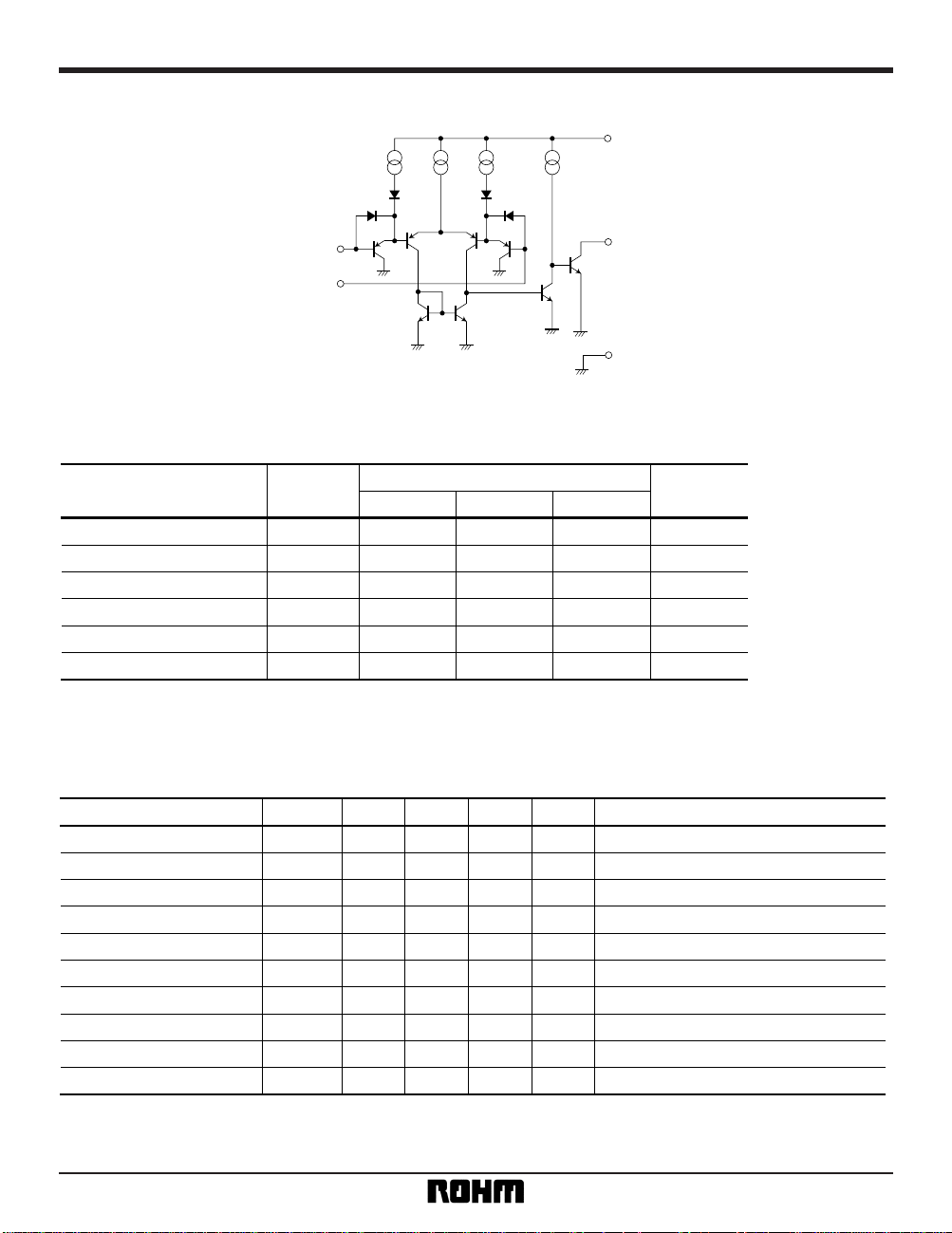
Internal circuit configuration
VCC
OUT
GND
+ IN
– IN
•
Absolute maximum ratings (Ta = 25°C)
Parameter Symbol
Limits
Unit
BA10393 BA10393F BA10393N
V
CC 36 ( ± 18) 36 ( ± 18) 36 ( ± 18) V
Pd 800
∗
550
∗
900
∗
mW
V
ID ± VCC V
V
I – 0.3 ~ VCC V
Topr °C
Tstg °C
– 40 ~ + 85
– 55 ~ + 125– 55 ~ + 125
– 40 ~ + 85– 40 ~ + 85
– 55 ~ + 125
± V
CC
– 0.3 ~ VCC
± VCC
– 0.3 ~ VCC
Power supply voltage
Power dissipation
Differential input voltage
Common-mode input voltage
Operating temperature
Storage temperature
∗
Refer to the Pd characteristics diagram.
The values for the BA10393F are those when it is mounted on a glass epoxy PCB (50mm × 50mm × 1.6mm).
•
Electrical characteristics (unless otherwise noted, Ta = 25°C, VCC = + 5V)
Parameter Symbol Min. Typ. Max. Unit Conditions
V
IO
— ± 1 ± 5mVV
O
= 1.4V
I
IO
— ± 5 ± 50 nA
| I
IN
+
+
+
+
– I
IN
–
|, VO = 1.4V
I
B
— 25 250 nA VO = 1.4V
V
ICM
0—VCC–1.5 V
A
V
93 106 — dB RL = 15kΩ, VCC = 15V
I
Q
— 0.4 1 mA RL = ∞, on All Comparators
I
sink
6 16 — mA VIN= + 1V, VIN= 0V, VO = 1.5V
V
OL
— 250 400 mV VIN= + 1V, VIN= 0V, I
sink
= 4mA
I
leak
— 0.1 — nA VIN= + 1V, VIN= 0V,VO = 5V
t
r
— 1.3 — µsRL = 5.1kΩ, VRL = 5V
I
nput offset voltage
Input offset current
Input bias current
Common-mode input voltage
Voltage gain
Quiescent current
Output sink current
Output saturation voltage
Output leakage current
Response time
–
–
–
Page 3

3
Standard ICs BA10393 / BA10393F / BA10393N
•
Electrical characteristic curves
Fig. 1 Power dissipation vs. ambient
temperature
POWER DISSIPATION: Pd (mW)
1200
1000
800
600
400
200
0
0 25 50 7585 100 125 150
AMBIENT TEMPERATURE: Ta (°C)
BA10393F
BA10393
BA10393N
INPUT BIAS CURRENT: IB (nA)
20
0
0
2010 30 40
POWER SUPPLY VOLTAGE: V
+
(V)
40
Ta = 25°C
Fig. 3 Input bias current vs. power
supply voltage
QUIESCENT CURRENT: IQ (mA)
0.2
0
0
2010 30 40
POWER SUPPLY VOLTAGE: V
+
(V)
0.6
0.8
Ta = 25°C
R
L = ∞
1.0
0.4
Fig. 2 Quiescent current vs. power
supply voltage
SATURATION VOLTAGE: VOL (V)
0.01
0.001
0.01
10.1 10 100
OUTPUT SINK CURRENT: I
O (mA)
0.1
1
10
Ta = 25°C
Fig. 4 Output saturation voltage vs.
output current
INPUT VOLTAGE
V
IN (mV)
50
0
100
0
1
3
4
5
2
1.0 1.5 2.00.50
TIME (µs)
OUTPUT VOLTAGE
VO
(V)
20mV
5mV
INPUT OVERDRIVE = 100mV
Fig. 6 Propagation characteristics (@)
INPUT VOLTAGE
V
IN (mV)
– 50
– 100
0
0
1
3
4
5
2
1.0 1.5 2.00.50
TIME (µs)
OUTPUT VOLTAGE
V
O (V)
100mV
20mV
5mV = INPUT OVERDRIVE
Fig. 5 Propagation characteristics (!)
Page 4

4
Standard ICs BA10393 / BA10393F / BA10393N
•
Operation notes
(1) Handling unused circuits
If a circuit is not in use, we recommend connecting it
as shown in Figure 7, so that its input is connected to
the potential within the in-phase input voltage range
(V
ICM) and the output is left open.
VCC
VEE
+
–
Fig. 7 Example of unused circuit connection
Open
(no connected)
To potential
in V
ICM
•
External dimensions (Units: mm)
DIP8 SOP8
SIP8
BA10393 BA10393F
BA10393N
0.4 ± 0.11.27
0.15
0.3Min.
0.15 ± 0.1
0.11
6.2 ± 0.3
4.4 ± 0.2
5.0 ± 0.2
85
41
1.5 ± 0.1
10.5 ± 0.5
1
8
2.54
3.5 ± 0.5
1.3
0.8
0.6
0.3 ± 0.1
2.8 ± 0.2
19.3 ± 0.2
1.2
5.8 ± 0.2
0.5 ± 0.1
3.2 ± 0.2 3.4 ± 0.3
85
14
9.3
± 0.3
6.5 ± 0.3
0.3
±
0.1
0.51Min.
2.54
0° ~ 15°
7.62
 Loading...