

Page 1
1
Standard ICs
Quad ground sense operational
amplifier
BA10324A / BA10324AF / BA10324AFV
The BA10324A, BA10324AF, and BA10324AFV are monolithic ICs with four built-in operational amplifiers featuring
internal phase compensation.
Either a dual or single power supply can be driven, and these products can be driven by a digital system 5V single
power supply. These products can be used in a wide range of administrative and industrial applications, including
transducer amplifiers and DC amplifiers.
•
Applications
Ground sensing type pre-amplifiers
Active filters
DC amplifiers
Pulse generators.
•
Features
1) Wide range of operating power supply voltages and
single power supply drive enabled.
(single power supply: 3 to 32V, dual power supply: ±
1.5 to ± 16V)
2) Common-mode input voltage can be operated from
the ground level.
3) Differential input voltage can be operated up to the
power supply voltage level.
4) Low current dissipation. (I
Q = 0.6mA)
5) Low offset voltage and offset current. (V
IO = 2mV, IIO
= 5nA typ.)
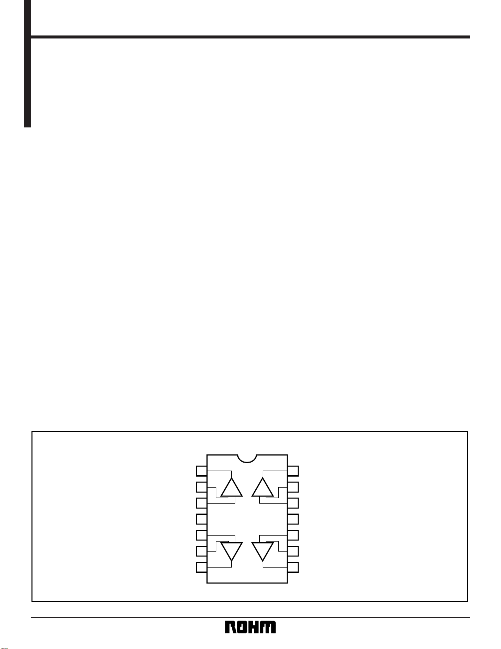
6) Four operational amplifiers with phase compensation are built into the DIP / SOP Pin 14.
7) Compatible with model 324 operational amplifiers of
other manufacturers.
•
Block diagram
1
2
1OUT1
– IN1
+ IN1
V
CC
+ IN2
–IN2
OUT2
OUT4
–IN4
+ IN4
V
EE
+ IN3
–IN3
OUT3
14
2
13
3
12
411
5
10
6
9
7
8
+–+–
3
+––+
4
BA10324A / BA10324AF / BA10324AFV
Page 2
2
Standard ICs BA10324A / BA10324AF / BA10324AFV
•
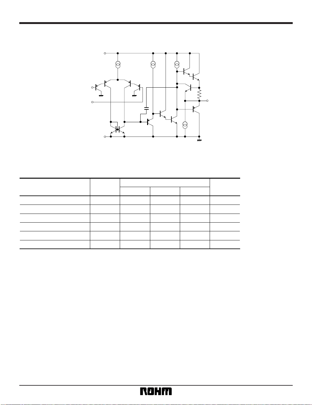
Internal circuit configuration
VCC
VEE
OUT
–IN
+ IN
•
Absolute maximum ratings (Ta = 25°C)
Parameter Symbol
Limits
Unit
BA10324A BA10324AF BA10324AFV
Power supply voltage
Power dissipation
Differential input voltage
Common-mode input voltage
Operating temperature
Storage temperature
V
CC 32 ( ± 16) 32 ( ± 16) 32 ( ± 16) V
950
∗
450
∗
400
∗
mW
V
ID ± VCC V
V
I – 0.3 ~ VCC V
Topr – 40 ~ + 85 – 40 ~ + 85 – 40 ~ + 85 °C
Tstg
– 55 ~ + 125 – 55 ~ + 125 – 55 ~ + 125
°C
Pd
± V
CC
– 0.3 ~ VCC
± VCC
– 0.3 ~ VCC
∗
Refer to the Pd characteristics diagram.
The values for the are those when BA10324AF / BA10324AFV it is mounted on a glass epoxy board (50mm × 50mm × 1.6mm).
Page 3

3
Standard ICs BA10324A / BA10324AF / BA10324AFV
•
Electrical characteristics (unless otherwise noted, Ta = 25°C, VCC = 5V)
Parameter Symbol Min. Typ. Max. Unit Conditions
V
IO
—2 7mVR
S
= 50Ω
I
IO
— 5 50 nA
Ib — 20 250 nA
V
ICM
0—V
CC
– 1.5
V
CC
– 1.5
V
CMRR 65 75 — dB
A
VOI
87 100 — dB
PSRR 65 100 — dB R
S
= 50Ω
I
Q
— 0.6 2.0 mA
V
OH
——VR
L
= 2kΩ
V
OL
— — 0.25 V RL = ∞
Source
Sink
I
OH
20 35 — mA VO = 0
I
OL
10 20 — mA VO = V
CC
CS — 120 — dB
f = 1kHz
input conversion
R
L
⭌ 2kΩ, VCC = 15V
R
L
= ∞, on All Op - Amps
∗
1
∗
1 Because the first stage is configured with a PNP transistor, input bias current is from the IC.
Input offset voltage
Input offset current
Input bias current
Common-mode input voltage
Common-mode rejection ratio
High-amplitude voltage gain
Power supply voltage rejection ratio
Quiescent current
Maximum output voltage
Maximum
output current
Channel separation
•
Electrical characteristic curves
1200
1000
800
600
400
200
0
0 25 50 75 85 100 125 150
AMBIENT TEMPERATURE: Ta (°C)
POWER DISSIPATION: Pd (mW)
Fig.1 Power dissipation vs. ambient
temperature
BA10324A
BA10324AF
BA10324AFV
2.0
1.5
1.0
0.5
010203040
POWER SUPPLY VOLTAGE: V
+
(V)
SUPPLY CURRENT: IQ (mA)
VCC
A
I
Q
+
–
Fig.2 Quiescent current vs. power
supply voltage
140
120
20
100
80
60
40
0
0 10 100 1k 10k 100k 1M 10M
FREQUENCY: f (Hz)
OPEN LOOP VOLTAGE GAIN: AV (dB)
10M
V
O
2
VCC
VIN
0.1µF
V
CC
+
–
~
Fig.3 Open loop voltage gain vs.
frequency
Page 4

4
Standard ICs BA10324A / BA10324AF / BA10324AFV
20
15
10
5
0
100 1k 10k 100k 1M
FREQUENCY: f (Hz)
MAXIMUM OUTPUT VOLTAGE: VOM (V)
100k
VO
VIN
2k
1k
7V
15V
~
+
–
Fig.4 Maximum output voltage vs.
frequency
50
40
0
– 20 0 20 40 60 80
10
20
30
AMBIENT TEMPERATURE: Ta (°C)
INPUT BIAS CURRET
:
I
B
(
nA)
Fig.5 Input bias current vs. ambient
temperature
40
0
10 20 30 40
10
20
30
POWER SUPPLY VOLTAGE: V
+
(V)
INPUT BIAS CURRENT: I
B
(nA)
Fig.6 Input bias current vs. power supply
voltage
5
3
2
4
0
0.001 0.01 0.1 1.0 10 100
1
OUTPUT SOURCE CURRENT (mA)
OUTPUT VOLTAGE
REFERENCED TO V
+
: ∆V (V)
Fig.7 Potential difference during
power supply output vs. output
source current
0.01
0.1
1.0
10
0.001 0.01 0.1 1.0 10 100 1000
OUTPUT SINK CURRENT: I
O
(mA)
OUTPUT VOLTAGE: V
O
(V)
Fig.8 Output voltage vs. output sink
current
RL ⭌ 2kΩ
V
CC
= 15V
4
3
2
1
0
0
020406080
1
2
3
TIME (µs)
INPUT VOLTAGE OUTPUT VOLTAGE
V
IN
(V) V
OUT
(V)
Fig.9 Output response characteristics
•
Operation notes
(1) Unused circuit connections
If there are any circuits which are not being used, we
recommend making connections as shown in Figure
10, with the non-inverted input pin connected to the
potential within the in-phase input voltage range (V
ICM).
VCC
VEE
+
–
Fig.10 Unused circuit connections
To potential
in V
ICM
Page 5

5
Standard ICs BA10324A / BA10324AF / BA10324AFV
BA10324A BA10324AF
BA10324AFV
DIP14 SOP14
SSOP-B14
6.5 ± 0.3
19.4 ± 0.3
0.5 ± 0.1
3.2 ± 0.2
4.25 ± 0.3
14 8
71
0.3 ± 0.1
0.51Min.
7.62
0° ~ 15°
2.54
0.4
± 0.11.27
1
14
8.7 ± 0.2
7
8
4.4 ± 0.2
6.2 ± 0.3
0.11
1.5 ± 0.1
0.15
0.15 ± 0.1
0.3Min.
0.1
0.22 ± 0.1
0.65
8
7
14
1
6.4 ± 0.3
4.4 ± 0.2
5.0 ± 0.2
1.15 ± 0.1
0.15 ± 0.1
0.3Min.
0.1
•
External dimensions (Units: mm)
 Loading...