

Page 1
Features
• Advanced, High-speed Programmable Logic Device – Superset of 22V10
– Improved Performance - 7.5 ns t
– Enhanced Logic Flexibility
– Backward Compatible with ATV750(L) Software and Hardware
• New Flip-flop Features
– D- or T-type
– Product Term or Direct Input Pin Clocking
• High-speed Erasable Programmable Logic Devices
– 7.5 ns Maximum Pin-to-pin Delay
Device ICC, Standby
ATV750B 125 mA
ATV750BL 15 mA
, 95 MHz External Operation
PD
High-speed UV
Erasable
Programmable
• Highest Density Programmable Logic Available in a 24-pin Package
• Increased Logic Flexibility
– 42 Array Inputs, 20 Sum Terms and 20 Flip-flops
• Enhanced Output Logic Flexibility
– All 20 Flip-flops Feed Back Internally
– 10 Flip-flops are Also Available as Outputs
• Full Military, Commercial and Industrial Temperature Ranges
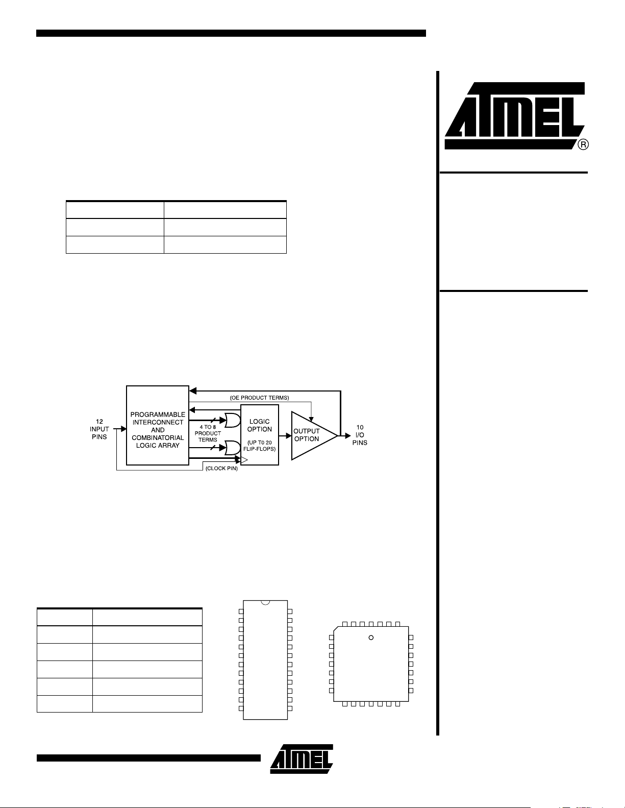
Logic Diagram
Description
The ATV750B(L) is twice as powerful as most other 24-pin programmable logic
devices. Increased product terms, sum terms, flip-flops and output logic configurations
translate into more usable gates. High-speed logic and uniform, predictable delays
guarantee fast in-system performance.
Logic Device
ATV750B
ATV750BL
Commercial and
industrial versions
are obsolete. Please
use ATF750C.
Military versions
continue to be available,
but please do not
use for new designs.
For new military
applications, recommend
multiple ATF22V10s.
Pin Configurations
Pin Name Function
CLK Clock
IN Logic Inputs
I/O Bi-directional Buffers
* No Internal Connection
V
CC
+5V Supply
CLK/IN
GND
DIP/SOIC
1
2
IN
3
IN
4
IN
5
IN
6
IN
7
IN
8
IN
9
IN
10
IN
11
IN
12
PLCC/LCC
24
VCC
23
I/O
22
I/O
21
I/O
20
I/O
19
I/O
18
I/O
17
I/O
16
I/O
15
I/O
14
I/O
13
IN
5
IN
6
IN
7
IN
8
*
9
IN
10
IN
11
IN
ININCLK/IN*VCC
432
12131415161718
IN
IN
GND
1
*
I/O
282726
IN
I/O
I/O
25
24
23
22
21
20
19
I/O
I/O
I/O
I/O
*
I/O
I/O
I/O
Rev. 0301I–08/01
1
Page 2
Each of the ATV750B(L) 22 logic pins can be used as an input. Ten of these can be used as
Combined Terms Separate Terms
inputs, outputs or bi-directional I/O pins. Each flip-flop is individually configurable as either Dor T-type. Each flip-flop output is fed back into the array independently. This allows burying of
all the sum terms and flip-flops.
There are 171 total product terms available. A variable format is used to assign between four
to eight product terms per sum term. There are two sum terms per output, providing added
flexibility. Much more logic can be replaced by this device than by any other 24-pin PLD. With
20 sum terms and flip-flops, complex state machines are easily implemented with logic to
spare.
Product terms provide individual clocks and asynchronous resets for each flip-flop. Each flipflop may also be individually configured to have direct input pin controlled clocking. Each output has its own enable product term. One product term provides a common synchronous
preset for all flip-flops. Register preload functions are provided to simplify testing. All registers
automatically reset upon power-up.
The ATV750BL is a low-power device with speeds as fast as 15 ns. The ATV750BL provides
the optimum low-power PLD solution, with full CMOS output levels. This device
significantly reduces total system power, thereby allowing battery-powered operation.
Absolute Maximum Ratings*
Temperature Under Bias................................ -55°C to +125°C
Storage Temperature..................................... -65°C to +150°C
Voltage on Any Pin with
Respect to Ground .........................................-2.0V to +7.0V
Voltage on Input Pins
with Respect to Ground
During Programming.....................................-2.0V to +14.0V
Programming Voltage with
Respect to Ground .......................................-2.0V to +14.0V
Integrated UV Erase Dose..............................7258 W•sec/cm
*NOTICE: Stresses beyond those listed under “Absolute
Maximum Ratings” may cause permanent damage to the device. This is a stress rating only and
functional operation of the device at these or any
(1)
(1)
(1)
2
Note: 1. Minimum voltage is -0.6V DC which may under-
other conditions beyond those indicated in the
operational sections of this specification is not
implied. Exposure to absolute maximum rating
conditions for extended periods may affect
device reliability.
shoot to -2.0V for pulses of less than
20 ns.Maximum output pin voltage is V
DC which may overshoot to +7.0V for pulses of
less than 20 ns.
+ 0.75V
CC
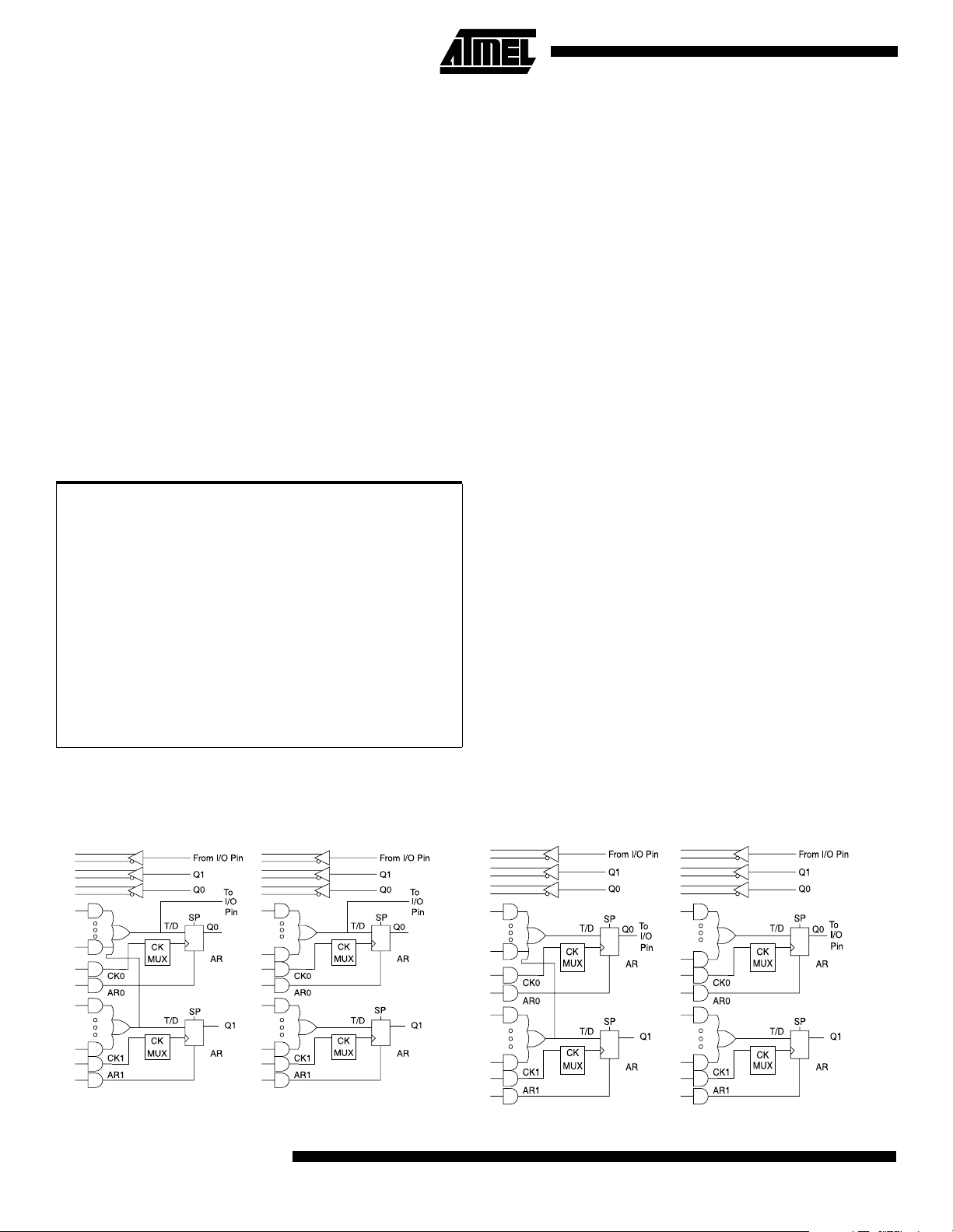
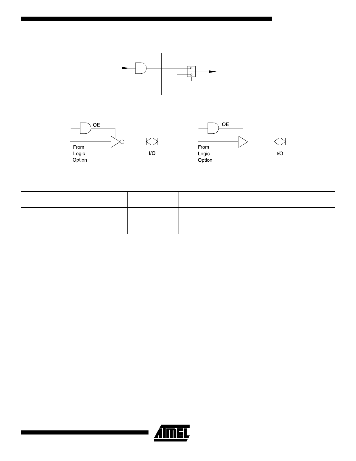
Logic Options
Combinatorial Output
2
ATV750B(L)
Registered Output
Combined Terms Separate Terms
0301I–08/01
Page 3
Clock Mux
C
Output Options
CLOCK
PRODUCT
TERM
CKi
CLK
PIN
ATV750B(L)
CK MUX
TO
LOGI
CELL
SELECT
DC and AC Operating Conditions
Operating Temperature 0°C - 70°C
V
Power Supply 5V ± 5% 5V ± 10% 5V ± 10% 5V ± 10%
CC
Note: 1. See ordering information for valid speed and temperature combination.
(1)
Commercial
-7, -10, -15
(Ambient)
Commercial
-25 Industrial Military
0°C - 70°C
(Ambient)
-40°C - 85°C
(Ambient)
-55°C - 125°C
(Case)
0301I–08/01
3
Page 4
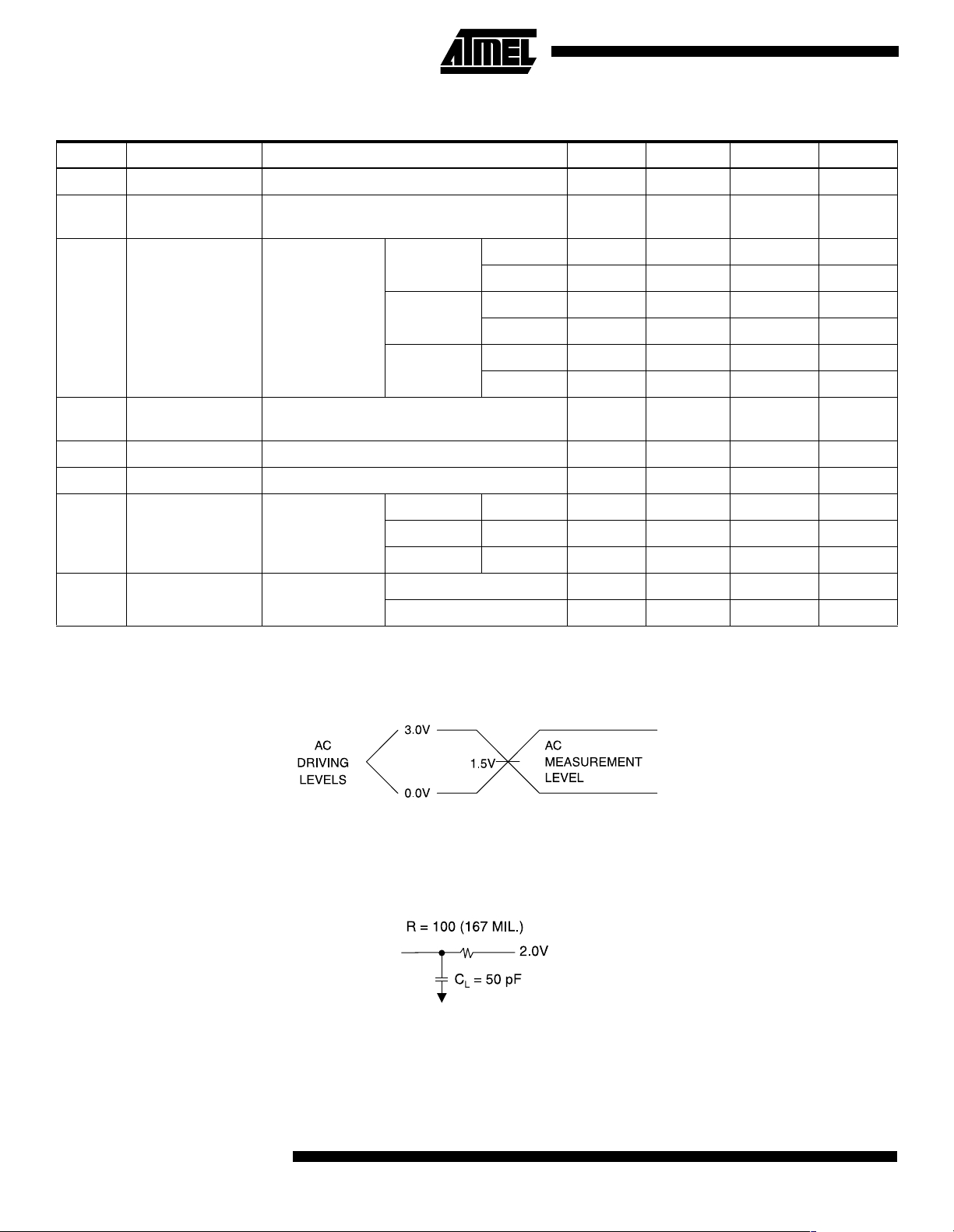
DC Characteristics
Symbol Parameter Condition Min Typ Max Units
I
LI
I
LO
Input Load Current VIN = -0.1V to VCC + 1V 10 µA
Output Leakage
Current V
= -0.1V to VCC + 0.1V
OUT
10 µA
Com. 125 180 mA
B-7, -10
Ind., Mil. 125 190 mA
Com. 125 180 mA
B-15, -25
= MAX,
V
Power Supply
I
CC
(1)
I
OS
V
IL
V
IH
Current, Standby
Output Short
Circuit Current V
Input Low Voltage 4.5 ≤ VCC ≤ 5.5V -0.6 0.8 V
Input High Voltage 2.0 V
Output Low
V
OL
Voltage
Output High
V
OH
Voltage
CC
= MAX,
V
IN
Outputs Open
= 0.5V
OUT
VIN = VIH or VIL,
V
= MIN
CC
VIN = VIH or VIL,
= MIN
V
CC
BL-15
= 16 mA Com., Ind. 0.5 V
I
OL
I
= 12 mA Mil. 0.5 V
OL
I
= 24 mA Com. 0.8 V
OL
= -100 µA VCC - 0.3 V
I
OH
I
= -4.0 mA 2.4 V
OH
Ind., Mil. 125 190 mA
Com. 15 30 mA
Ind., Mil. 15 30 mA
-120 mA
+ 0.75 V
CC
Note: 1. Not more than one output at a time should be shorted. Duration of short circuit test should not exceed 30 sec.
Input Test Waveforms and Measurement Levels
Output Test Load
4
ATV750B(L)
tR, tF < 3 ns (10% to 90%)
0301I–08/01
Page 5
ATV750B(L)
AC Waveforms, Product Term Clock
(1)
Note: 1. Timing measurement reference is 1.5V. Input AC driving levels are 0.0V and 3.0V, unless otherwise specified.
AC Characteristics, Product Term Clock
(1)
-7 -10 B/BL-15 B/BL-25
Symbol Parameter
UnitsMin Max Min Max Min Max Min Max
t
PD
t
EA
t
ER
t
CO
t
CF
t
S
t
SF
t
H
t
P
t
W
f
MAX
t
AW
t
AR
t
AP
Input or Feedback to
7.5 10 15 25 ns
Non-Registered Output
Input to Output Enable 7.5 10 15 25 ns
Input to Output Disable 7.5 10 15 25 ns
Clock to Output 3 7.5 4 10 5 12 6 20 ns
Clock to Feedback 1 5 4 7.5 5 9 5 10 ns
Input Setup Time 3 4 8/12 14 ns
Feedback Setup Time 3 4 7 7 ns
Hold Time 1 2 5/7 5/7 ns
Clock Period 7 11 14 17 ns
Clock Width 3.5 5.5 7 8.5 ns
External Feedback 1/(tS+tCO) 95 71 50/41 29 MHz
Internal Feedback 1/(t
No Feedback 1/(t
) 142 90 71 58 MHz
P
) 125 86 62 58 MHz
SF+tCF
Asynchronous Reset Width 5 10 15 20 ns
Asynchronous Reset
31015 20 ns
Recovery Time
Asynchronous Reset to
812 1525ns
Registered Output Reset
t
SP
Setup Time, Synchronous Preset 4 7 8 15 ns
Note: 1. See ordering information for valid part numbers.
0301I–08/01
5
Page 6
AC Waveforms, Input Pin Clock
(1)
Note: 1. Timing measurement reference is 1.5V. Input AC driving levels are 0.0V and 3.0V, unless otherwise specified.
AC Characteristics, Input Pin Clock
Symbol Parameter
Input or Feedback to
t
PD
t
EA
t
ER
t
COS
t
CFS
t
SS
t
SFS
t
HS
t
PS
t
WS
f
MAXS
Non-Registered Output
Input to Output Enable 7.5 10 15 25 ns
Input to Output Disable 7.5 10 15 25 ns
Clock to Output 0 6.5 0 7 0 10 0 12 ns
Clock to Feedback 0 3.5 0 5 0 5.5 0 7 ns
Input Setup Time 4 6.5 8/12.5 9/15 ns
Feedback Setup Time 4 5 7 9 ns
Hold Time 0 0 0 0 ns
Clock Period 7 10 12 16 ns
Clock Width 3.5 5 6 8 ns
External Feedback 1/(tSS+t
Internal Feedback 1/(t
No Feedback 1/(tPS) 142 100 83 62 MHz
t
t
AW
ARS
Asynchronous Reset Width 5 10 15 20 ns
Asynchronous Reset
Recovery Time
COS
SFS+tCFS
-7 -10
B/BL
-15
B/BL
-25
UnitsMin Max Min Max Min Max Min Max
7.5 10 15 25 ns
) 95 74 55/44 48/37 MHz
) 133 100 80 62 MHz
510 15 25 ns
t
AP
Asynchronous Reset to
810 15 25ns
Registered Output Reset
t
SPS
6
Setup Time, Synchronous Preset 5 5/9 11 15 ns
ATV750B(L)
0301I–08/01
Page 7

Functional Logic Diagram ATV750B, Upper Half
ATV750B(L)
0301I–08/01
7
Page 8

Functional Logic Diagram ATV750B, Lower Half
8
ATV750B(L)
0301I–08/01
Page 9

ATV750B(L)
Preload of Registered Outputs
The ATV750B(L) registers are provided with circuitry to allow loading of each register asynchronously with either a high or a low. This feature will simplify testing since any state can be
forced into the registers to control test sequencing. A V
ister high; a V
will force it low, independent of the output polarity. The PRELOAD state is
IL
level on the I/O pin will force the reg-
IH
entered by placing a 10.25V to 10.75V signal on pin 8 on DIPs, and lead 10 on SMDs. When
the clock term is pulsed high, the data on the I/O pins is placed into the register chosen by the
Select Pin.
Level Forced on Registered
Output Pin during
PRELOAD Cycle
V
IH
V
IL
V
IH
V
IL
Select Pin
State
Low High X
Low Low X
High X High
High X Low
Register #0 State after
Cycle
Register #1 State after
Cycle
0301I–08/01
9
Page 10

Power-up Reset The registers in the ATV750B(L) is designed to reset during power-up. At a point delayed
slightly from V
crossing V
CC
depend on the polarity of the output buffer.
This feature is critical for state machine initialization. However, due to the asynchronous
nature of reset and the uncertainty of how V
tions are required:
1. The V
rise must be monotonic,
CC
2. After reset occurs, all input and feedback setup times must be met before driving the
clock terms or pin high, and
3. The clock pin, or signals from which clock terms are derived, must remain stable during
.
t
PR
, all registers will be reset to the low state. The output state will
RST
actually rises in the system, the following condi-
CC
Parameter Description Typ Max Units
t
PR
V
RST
Power-up Reset Time 600 1000 ns
Power-up Reset Voltage 3.8 4.5 V
Pin Capacitance
f = 1 MHz, T = 25°C
C
IN
C
OUT
(1)
Typ Max Units Conditions
58 pF V
68 pF V
IN
OUT
= 0V
= 0V
10
ATV750B(L)
0301I–08/01
Page 11

ATV750B(L)
Using the ATV750B(L) Many Advanced Features
Programming Software Support
The ATV750B(L) advanced flexibility packs more usable gates into 24-pins than any other
logic device. The ATV750B(L) starts with the popular 22V10 architecture, and add several
enhanced features:
• Selectable D- and T-type Registers – Each ATV750B flip-flop can be individually
configured as either D- or T-type. Using the T-type configuration, JK and SR flip-flops are
also easily created. These options allow more efficient product term usage.
• Selectable Asynchronous Clocks – Each of the ATV750B(L) flip-flops may be clocked
by its own clock product term or directly from Pin 1 (SMD Lead 2). This removes the
constraint that all registers must use the same clock. Buried state machines, counters and
registers can all coexist in one device while running on separate clocks. Individual flip-flop
clock source selection further allows mixing higher performance pin clocking and flexible
product term clocking within one design.
• A Full Bank of Ten More Registers – The ATV750B provides two flip-flops per output
logic cell for a total of 20. Each register has its own sum term, its own reset term and its
own clock term.
• Independent I/O Pin and Feedback Paths – Each I/O pin on the ATV750B has a
dedicated input path. Each of the 20 registers has its own feedback terms into the array
as well. This feature, combined with individual product terms for each I/O’s output enable,
facilitates true bi-directional I/O design.
As with all other Atmel PLDs, several third-party development software products support the
ATV750B(L). Several third-party programmers support the ATV750B as well. Additionally, the
ATV750B may be programmed to perform the ATV750(L)’s functional subset (no T-type flipflops or pin clocking) using the ATV750(L) JEDEC file. In this case, the ATV750B becomes a
direct replacement or speed upgrade for the ATV750(L). The ATV750(L) programming algorithm is different from the ATV750B algorithm. Choose the appropriate device in your
programmer menu to ensure proper programming. Please refer to the Programmable Logic
Development Tools section for a complete PLD software and programmer listing.
Synchronous Preset and Asynchronous Reset
Security Fuse Usage
One synchronous preset line is provided for all 20 registers in the ATV750B. The appropriate
input signals to cause the internal clocks to go to a high state must be received during a synchronous preset. Appropriate setup and hold times must be met, as shown in the switching
waveform diagram.
An individual asynchronous reset line is provided for each of the 20 flip-flops. Both master and
slave halves of the flip-flops are reset when the input signals received force the internal resets
high.
A single fuse is provided to prevent unauthorized copying of the ATV750B fuse patterns. Once
the security fuse is programmed, all fuses will appear programmed during verify.
The security fuse should be programmed last, as its effect is immediate.
0301I–08/01
11
Page 12

Erasure Characteristics
The entire memory array of an ATV750B is erased after exposure to ultraviolet light at a wavelength of 2537 Å. Complete erasure is assured after a minimum of 20 minutes exposure using
12,000 µW/cm
lamps at other intensity ratings can be calculated from the minimum integrated erasure dose
of 15 W
the clear window on any UV-erasable PLD which will be subjected to continuous fluorescent
indoor lighting or sunlight.
•sec/cm
2
intensity lamps spaced one inch away from the chip. Minimum erase time for
2
. To prevent unintentional erasure, an opaque label is recommended to cover
Atmel CMOS PLDs
The ATV750B utilizes an advanced 0.65-micron CMOS EPROM technology. This technology’s state-of-art features are the optimum combination for PLDs:
• CMOS technology provides high-speed, low-power, and high noise immunity.
• EPROM technology is the most cos-effective method for producing PLDs – surpassing
bipolar fusible link technology in low cost, while providing the necessary
reprogrammability.
• EPROM reprogrammability, which is 100% tested before shipment, provides inherently
better programmability and reliability than one-time fusible PLDs.
12
ATV750B(L)
0301I–08/01
Page 13

ATV750B(L)
0301I–08/01
13
Page 14

14
ATV750B(L)
0301I–08/01
Page 15

Ordering Information
Ext.
t
PD
(ns)
t
COS
(ns)
7.5 6.5 95
10 7 74
15 10 58
25 15 41
10 7 74 5962-88726 08 LA
15 9 58 5962-88726 09 LA
Notes: 1. Obsolete, please use ATF750C versions.
2. Continue to be available, but please do not use for new designs. For new designs recommend multiple ATF22V10s.
f
MAXS
(MHz) Ordering Code Package Operation Range
ATV750B-7JC
ATV750B-7PC
ATV750B-10JC
ATV750B-10PC
ATV750B-10SC
ATV750B-10JI
ATV750B-10PI
ATV750B-10SI
ATV750B-10DM/883
ATV750B-10LM/883
ATV750B-15JC
ATV750B-15PC
ATV750B-15SC
ATV750B-15JI
ATV750B-15PI
ATV750B-15SI
ATV750B-15DM/883
ATV750B-15LM/883
ATV750B-25JC
ATV750B-25PC
ATV750B-25SC
ATV750B-25JI
ATV750B-25PI
ATV750B-25SI
5962-88726 08 3X
5962-88726 09 3X
ATV750B(L)
(1)
(1)
(1)
(1)
(1)
(1)
(1)
(1)
(2)
(2)
(1)
(1)
(1)
(1)
(1)
(1)
(2)
(2)
(1)
(1)
(1)
(1)
(1)
(1)
(2)
(2)
(2)
(2)
28J
24P3
28J
24P3
24S
28J
24P3
24S
24DW3
28LW
28J
24P3
24S
28J
24P3
24S
24DW3
28LW
28J
24P3
24S
28J
24P3
24S
24DW3
28LW
24DW3
28LW
Commercial
(0°C to 70°C)
Commercial
(0°C to 70°C)
Industrial
(-40°C to 85°C)
Military/883C
(-55°C to 125°C)
Class B, Fully Compliant
Commercial
(0°C to 70°C)
Industrial
(-40°C to 85°C)
Military/883C
(-55°C to 125°C)
Class B, Fully Compliant
Commercial
(0°C to 70°C)
Industrial
(-40°C to 85°C)
Military/883C
(-55°C to 125°C)
Class B, Fully Compliant
Military/883C
(-55°C to 125°C)
Class B, Fully Compliant
0301I–08/01
15
Page 16

Ordering Information (Continued)
Ext.
t
PD
(ns)
15 9 92 ATV750BL-15JC
25 15 37
t
COS
(ns)
f
MAXS
(MHz) Ordering Code Package Operation Range
ATV750BL-15PC
ATV750BL-15SC
ATV750BL-15JI
ATV750BL-15PI
ATV750BL-15SI
ATV750BL-15DM/883
ATV750BL-15LM/883
ATV750BL-25JC
ATV750BL-25PC
ATV750BL-25SC
(1)
(1)
(1)
(1)
(1)
(1)
(2)
(2)
28J
24P3
24S
28J
24P3
24S
24DW3
28LW
Commercial
(0°C to 70°C)
Industrial
(-40°C to 85°C)
Military/883C
(-55°C to 125°C)
Class B, Fully Compliant
(1)
(1)
(1)
28J
24P3
24S
Commercial
(0°C to 70°C)
ATV750BL-25JI19
ATV750BL-25PI
ATV750BL-25SI
(1)
(1)
15 9 92 5962-88726 11 LX
5962-88726 11 3X
(2)
(2)
28J
24P3
24S
24DW3
28LW
Industrial
(-40°C to 85°C)
Military/883C
(-55°C to 125°C)
Class B, Fully Compliant
Notes: 1. Obsolete, please use ATF750C versions.
2. Continue to be available, but please do not use for new designs. For new designs recommend multiple ATF22V10s.
Using “C” Product for Industrial
To use commercial product for Industrial temperature ranges, down-grade one speed grade from the “I” to the “C” device
(7 ns “C” = 10 ns “I”) and de-rate power by 30%.
Package Type
24DW3 24-lead, 0.300" Wide, Windowed, Ceramic Dual Inline Package (Cerdip)
28J 28-lead, Plastic J-leaded Chip Carrier OTP (PLCC)
28LW 28-pad, Windowed, Ceramic Leadless Chip Carrier (LCC)
24P3 24-lead, 0.300" Wide, Plastic Dual Inline Package OTP (PDIP)
24S 24-lead, 0.300" Wide, Plastic Gull Wing Small Outline OTP (SOIC)
16
ATV750B(L)
0301I–08/01
Page 17

Packaging Information
(
ATV750B(L)
24DW3, 24-lead, 0.300" Wide, WIndowed, Ceramic
Dual Inline Package (Cerdip)
Dimensions in Inches and (Millimeters)
MIL-STD-1835 D-9 CONFIG A
28J, 28-lead, Plastic J-leaded Chip Carrier (PLCC)
Dimensions in Inches and (Millimeters)
JEDEC STANDARD MS-018 AB
.045
.045(1.14) X 45°
.032(.813)
.026(.660)
.050(1.27) TYP
PIN NO. 1
IDENTIFY
.300(7.62) REF SQ
1.14) X 30° - 45°
.456(11.6)
.450(11.4)
SQ
.495(12.6)
.485(12.3)
.022(.559) X 45° MAX (3X)
SQ
.012(.305)
.008(.203)
.430(10.9)
.390(9.91)
.021(.533)
.013(.330)
.043(1.09)
.020(.508)
.120(3.05)
.090(2.29)
.180(4.57)
.165(4.19)
SQ
28LW, 28-pad, Windowed, Ceramic Leadless Chip
Carrier (LCC)
Dimensions in Inches and (Millimeters)*
MIL-STD-1835 C-4
*Controlling dimension: millimeters
24P3, 24-lead, 0.300" Wide, Plastic Dual Inline
Package (PDIP)
Dimensions in Inches and (Millimeters)
JEDEC STANDARD MS-001 AF
1.27(32.3)
.200(5.06)
SEATING
PLANE
MAX
.151(3.84)
.125(3.18)
.110(2.79)
.090(2.29)
.012(.305)
.008(.203)
1.25(31.7)
1.100(27.94) REF
PIN
1
.065(1.65)
.040(1.02)
.325(8.26)
.300(7.62)
0
REF
15
.400(10.2) MAX
.090(2.29)
.005(.127)
.070(1.78)
.020(.508)
.023(.584)
.014(.356)
.266(6.76)
.250(6.35)
MAX
MIN
0301I–08/01
17
Page 18

Packaging Information
24S, 24-lead, 0.300" Wide, Plastic Gull Wing Small
Outline (SOIC)
Dimensions in Inches and (Millimeters)
.020(.508)
.013(.330)
ATV750B(L)
PIN 1 ID
.616(15.6)
.598(15.2)
0
REF
8
.299(7.60)
.291(7.39)
.050(1.27) BSC
.012(.305)
.003(.076)
.050(1.27)
.015(.381)
.420(10.7)
.393(9.98)
.105(2.67)
.092(2.34)
.013(.330)
.009(.229)
0301I–08/01
18
Page 19

Atmel Headquarters Atmel Product Operations
Corporate Headquarters
2325 Orchard Parkway
San Jose, CA 95131
TEL (408) 441-0311
FAX (408) 487-2600
Europe
Atmel SarL
Route des Arsenaux 41
Casa Postale 80
CH-1705 Fribourg
Switzerland
TEL (41) 26-426-5555
FAX (41) 26-426-5500
Asia
Atmel Asia, Ltd.
Room 1219
Chinachem Golden Plaza
77 Mody Road Tsimhatsui
East Kowloon
Hong Kong
TEL (852) 2721-9778
FAX (852) 2722-1369
Japan
Atmel Japan K.K.
9F, Tonetsu Shinkawa Bldg.
1-24-8 Shinkawa
Chuo-ku, Tokyo 104-0033
Japan
TEL (81) 3-3523-3551
FAX (81) 3-3523-7581
Atmel Colorado Springs
1150 E. Cheyenne Mtn. Blvd.
Colorado Springs, CO 80906
TEL (719) 576-3300
FAX (719) 540-1759
Atmel Grenoble
Avenue de Rochepleine
BP 123
38521 Saint-Egreve Cedex, France
TEL (33) 4-7658-3000
FAX (33) 4-7658-3480
Atmel Heilbronn
Theresienstrasse 2
POB 3535
D-74025 Heilbronn, Germany
TEL (49) 71 31 67 25 94
FAX (49) 71 31 67 24 23
Atmel Nantes
La Chantrerie
BP 70602
44306 Nantes Cedex 3, France
TEL (33) 0 2 40 18 18 18
FAX (33) 0 2 40 18 19 60
Atmel Rousset
Zone Industrielle
13106 Rousset Cedex, France
TEL (33) 4-4253-6000
FAX (33) 4-4253-6001
Atmel Smart Card ICs
Scottish Enterprise Technology Park
East Kilbride, Scotland G75 0QR
TEL (44) 1355-357-000
FAX (44) 1355-242-743
e-mail
literature@atmel.com
Web Site
http://www.atmel.com
BBS
1-(408) 436-4309
© Atmel Corporation 2001.
Atmel Corporation makes no warranty for the use of its products, other than those expressly contained in the Company’s standard warranty
which is detailed in Atmel’s Terms and Conditions located on the Company’s web site. The Company assumes no responsibility for any errors
which may appear in this document, reserves the right to change devices or specifications detailed herein at any time without notice, and does
not make any commitment to update the information contained herein. No licenses to patents or other intellectual property of Atmel are granted
by the Company in connection with the sale of Atmel products, expressly or by implication. Atmel’s products are not authorized for use as critical
components in life support devices or systems.
ATME L® is the registered trademark of Atmel.
Other terms and product names may be the trademarks of others.
Printed on recycled paper.
0301I–08/01/xM
 Loading...