

Page 1
Features
• High-performance, High-density Programmable Logic Device
– Typical 7 ns Pin-to-pin Delay
– Fully Connected Logic Array with 416 Product Terms
• Flexible Output Macrocell
– 48 Flip-flops – Two per Macrocell
–72 Sum Terms
– All Flip-flops, I/O Pins Feed in Independently
– Achieves Over 80% Gate Utilization
• Enhanced Macrocell Configuration Selections
– D- or T-type Flip-flops
– Product Term or Direct Input Pin Clocking
– Registered or Combinatorial Internal Feedback
• Several Power Saving Options
Device ICC, Standby
High-speed
High-density
UV-erasable
ATV2500B 110 mA
ATV2500BQ 30 mA
ATV2500BL 2 mA
ATV2500BQL 2 mA
• Backward Compatible with ATV2500H/L Software
• Proven and Reliable High-speed UV EPROM Process
• Reprogrammable – Tested 100% for Programmability
• 40-lead Dual-in-line and 44-lead Surface Mount Packages
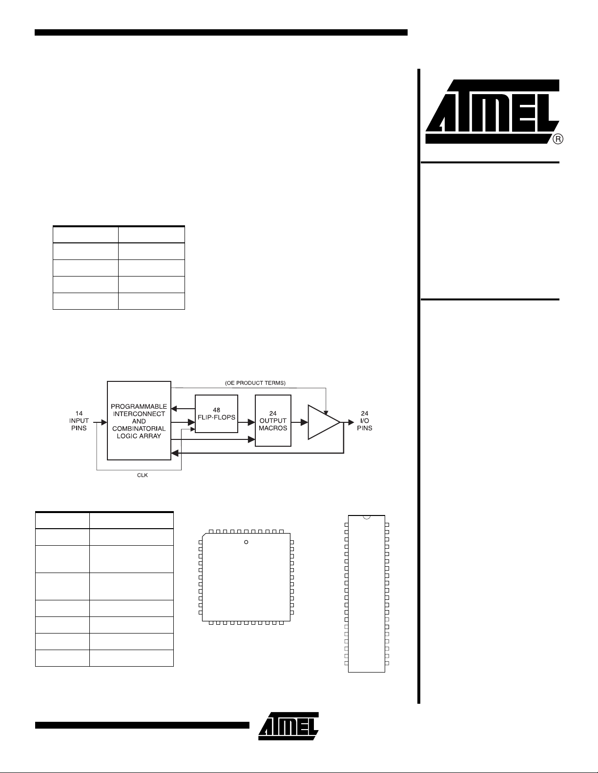
Block Diagram
Pin Configurations
Pin Name Function
IN Logic Inputs
CLK/IN Pin Clock and
Input
I/O Bi-directional
Buffers
I/O 0,2,4.. “Even” I/O Buffers
I/O 1,3,5.. “Odd” I/O Buffers
GND Ground
VCC +5V Supply
Note: For ATV2500BQ and
ATV2500BQL (PLCC/LCC
package only) pin 4 and
pin 26 connections are not
required.
I/O2
I/O3
I/O4
I/O5
VCC
VCC
I/O17
I/O16
I/O15
I/O14
I/O13
LCC/PLCC
I/O1
I/O0
GNDININ
65432
7
8
9
10
11
12
13
14
15
16
17
1819202122232425262728
I/O12
CLK/INININININ
1
4443424140
INININININININ
GND
I/O18
I/O06
39
38
37
36
35
34
33
32
31
30
29
I/O19
I/O7
I/O8
I/O9
I/O10
I/O11
GND
GND
I/O23
I/O22
I/O21
I/O20
CLK/IN
I/O0
I/O1
I/O2
I/O3
I/O4
I/O5
VCC
I/O17
I/O16
I/O15
I/O14
I/O13
I/O12
Programmable
Logic Device
ATV2500B
ATV2500BQ
ATV2500BQL
DIP
1
40
2
IN
3
IN
4
5
6
7
8
9
10
11
12
13
14
15
16
17
IN
18
IN
19
IN
20
IN
IN
39
IN
38
IN
37
IN
36
I/O6
35
I/O7
34
I/O8
33
I/O9
32
I/O10
31
I/O11
30
GND
29
I/O23
28
I/O22
27
I/O21
26
I/O20
25
I/O19
24
I/O18
23
IN
22
IN
21
IN
Rev. 0249J–05/00
1
Page 2
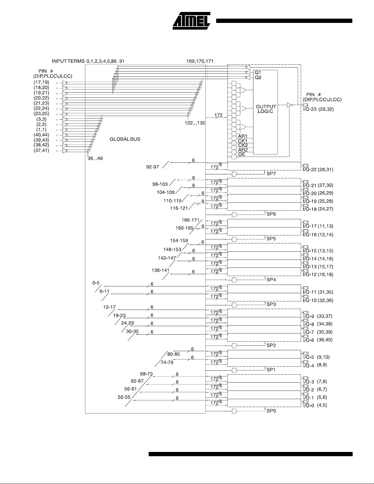
Functional Logic Diagram ATV2500B
Note: 1. Not required for PLCC versions of ATV2500BQ or ATV2500BQL, making them compatible with ATV2500H and ATV2500L
pinout.
2
ATV2500B(Q)(L)
Page 3

ATV2500B(Q)(L)
Description
The ATV2500Bs are the highest density PLDs available in
a 40- or 44-lead package. With their fully connected logic
array and flexible macrocell structure, high-gate utilization
is easily obtainable.
The ATV2500Bs are organized around a single universal
and-or array. All pins and feedback terms are always available to every macrocell. Each of the 38 logic pins are array
inputs, as are the outputs of each flip-flop.
In the ATV2500Bs, four product terms are input to each
sum term. Furthermore, each macrocell’s three sum terms
can be combined to provide up to 12 product terms per
sum term with no performance penalty. Each flip-flop is
individually selectable to be either D- or T-type, providing
further logic compaction. Also, 24 of the flip-flops may be
bypassed to provide internal combinatorial feedback to the
logic array.
Product terms provide individual clocks and asynchronous
resets for each flip-flop. The flip-flops may also be individually configured to have direct input pin clocking. Each
output has its own enable product term. Eight synchronous
preset product terms serve local groups of either four or
eight flip-flops. Register preload functions are provided to
simplify testing. All registers automatically reset upon
power-up.
Several low-power device options allow selection of the
optimum solution for many power-sensitive applications.
Each of the options significantly reduces total system
power and enhances system reliability.
Functional Logic Diagram Description
The ATV2500B functional logic diagram describes the
interconnections between the input, feedback pins and
logic cells. All interconnections are routed through the
single global bus.
The ATV2500Bs are straightforward and uniform PLDs.
The 24 macrocells are numbered 0 through 23. Each macrocell contains 17 AND gates. All AND gates have 172
inputs. The five lower product terms provide AR1, CK1,
CK2, AR2, and OE. These are: one asynchronous reset
and clock per flip-flop, and an output enable. The top 12
product terms are grouped into three sum terms, which are
used as shown in the macrocell diagrams.
Eight synchronous preset terms are distributed in a 2/4 pattern. The first four macrocells share Preset 0, the next two
share Preset 1, and so on, ending with the last two macrocells sharing Preset 7.
The 14 dedicated inputs and their complements use the
numbered positions in the global bus as shown. Each macrocell provides six inputs to the global bus: (left to right)
feedback F2
and the pin true and false. The positions occupied by these
signals in the global bus are the six numbers in the bus diagram next to each macrocell.
Note: 1. Either the flip-flop input (D/T2) or output (Q2) may be
(1)
true and false, flip-flop Q1 true and false,
3
Page 4
Absolute Maximum Ratings*
Temperature Under Bias................................ -55°C to +125°C
Storage Temperature..................................... -65°C to +150°C
Voltage on Any Pin with
Respect to Ground .........................................-2.0V to +7.0V
Voltage on Input Pins
with Respect to Ground
During Programming.....................................-2.0V to +14.0V
Programming Voltage with
Respect to Ground .......................................-2.0V to +14.0V
Integrated UV Erase Dose..............................7258 W•sec/cm
(1)
(1)
(1)
2
*NOTICE: Stresses beyond those listed under “Absolute
Maximum Ratings” may cause permanent damage to the device. This is a stress rating only and
functional operation of the device at these or any
other conditions beyond those indicated in the
operational sections of this specification is not
implied. Exposure to absolute maximum rating
conditions for extended periods may affect device
reliability.
Note: 1. Minimum voltage is -0.6V DC which may under-
shoot to -2.0V for pulses of less than 20 ns.
Maximum output pin voltage is V
CC
which may overshoot to +7.0V for pulses of less
than 20 ns.
DC and AC Operating Conditions
Commercial Industrial Military
Operating Temperature
0°C - 70°C
(Ambient)
VCC Power Supply 5V ± 5% 5V ± 10% 5V ± 10%
-40°C - 85°C
(Ambient)
-55°C - 125°C
(Case)
+ 0.75V DC
Pin Capacitance
f = 1 MHz, T = 25°C
C
IN
C
OUT
Note: 1. Typical values for nominal supply voltage. This parameter is only sampled and is not 100% tested.
(1)
Typ Max Units Conditions
46pFV
812pFV
= 0V
IN
OUT
= 0V
4
ATV2500B(Q)(L)
Page 5
ATV2500B(Q)(L)
Output Logic, Registered
(1)
S2 = 0 Terms in
Output ConfigurationS1 S0 D/T1 D/T2
0084Registered (Q1); Q2 FB
(1)
10124
1184Registered (Q1); D/T2 FB
Output
S3
Configuration S6 Q1 CLOCK
0 Active Low 0 CK1
1 Active High 1 CK1 • PIN1
S4 Register 1 Type S7 Q2 CLOCK
0D 0CK2
1T 1CK2 • PIN1
S5 Register 2 Type
0D
1T
Registered (Q1); Q2 FB
Output Logic, Combinatiorial
(1)
Note: 1. These diagrams show equivalent logic functions, not
necessarily the actual circuit implementation.
S2 = 1 Terms in
Output ConfigurationS5 S1 S0 D/T1 D/T2
X004
X0144
X104
1114
01144
(1)
(1)
(1)
Combinatorial (8 Terms);
4
Q2 FB
Combinatorial (4 Terms);
Q2 FB
Combinatorial (12 Terms);
(1)
4
Q2 FB
Combinatorial (8 Terms);
4
D/T2 FB
Combinatorial (4 Terms);
D/T2 FB
Note: 1. These four terms are shared with D/T1.
Clock Option
5
Page 6
DC Characteristics
Symbol Parameter Condition Min Typ Max Units
I
IL
I
LO
Input Load Current VIN = -0.1V to VCC + 1V 10 µA
Output Leakage
Current
= -0.1V to VCC + 0.1V 10 µA
V
OUT
Com. 110 190 mA
ATV2500B
Ind., Mil. 110 210 mA
= MAX,
V
Power Supply
I
CC
Current,
Standby
CC
V
= GND or
IN
f = 0 MHz,
V
CC
Outputs Open
ATV2500BQ
ATV2500BL
ATV2500BQL
I
OS
V
IL
V
IH
V
OL
V
OH
Output Short
Circuit Current
V
= 0.5V -120 mA
OUT
Input Low Voltage MIN ≤ VCC ≤ MAX -0.6 0.8 V
Input High Voltage 2.0
Output Low
Voltage
Output High
Voltage
VIN = VIH or VIL,
= 4.5V
V
CC
= MIN
V
CC
IOL = 8 mA Com., Ind. 0.5 V
I
= 6 mA Mil. 0.5 V
OL
I
= -100 µA VCC - 0.3 V
OH
I
= -4.0 mA 2.4
OH
Note: 1. See ICC versus frequency characterization curves.
Com. 30 70 mA
Ind., Mil. 30 85 mA
Com. 2 5 mA
Ind., Mil. 2 10 mA
Com. 2 4 mA
Ind., Mil. 2 5 mA
VCC +
0.75
V
6
ATV2500B(Q)(L)
Page 7
ATV2500B(Q)(L)
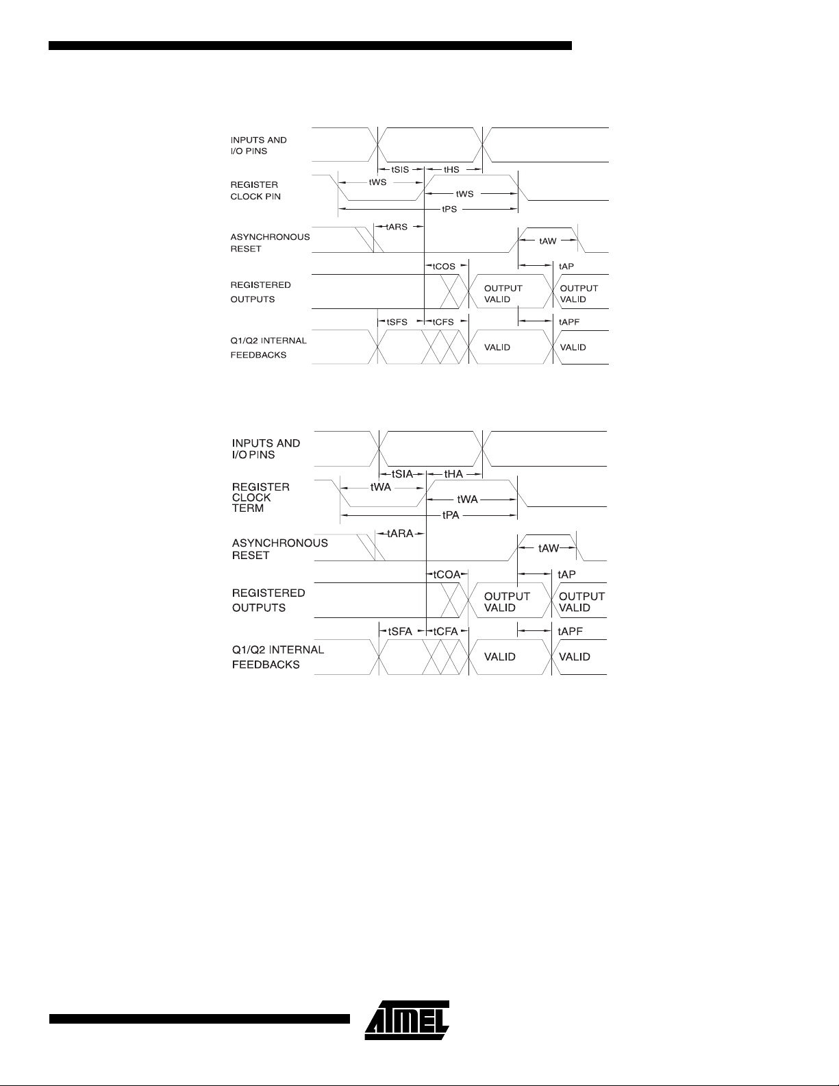
AC Waveforms
AC Waveforms
(1)
Input Pin Clock
(1)
Product Term Clock
Note: 1. Timing measurement reference is 1.5V. Input AC driving levels are 0.0V and 3.0V, unless otherwise specified.
7
Page 8

Register AC Characteristics, Input Pin Clock
-12 -15 -20 -25 -30
Symbol Parameter
t
COS
t
CFS
t
SIS
t
SFS
t
HS
t
WS
t
PS
Clock to Output 7.510111215ns
Clock to Feedback 0405060708 ns
Input Setup Time 7 9 14 20 23 ns
Feedback Setup Time 7 9 14 20 23 ns
Hold Time 00000 ns
Clock Width 56789 ns
Clock Period 10 12 14 16 18 ns
External Feedback 1/(t
F
MAXS
Internal Feedback 1/(t
No Feedback 1/(t
t
ARS
Asynchronous Reset/Preset
Recovery Time
+ t
SIS
COS
+ t
SFS
CFS
) 100 83 71 62 55 MHz
PS
Min Max Min Max Min Max Min Max Min Max
)6952403126MHz
)9071503732MHz
7 12152025 ns
Units
8
ATV2500B(Q)(L)
Page 9

Register AC Characteristics, Product Term Clock
-12 -15 -20 -25 -30
Symbol Parameter
t
COA
t
CFA
t
SIA
t
SFA
t
HA
t
WA
t
PA
Clock to Output 12 15 20 22 25 ns
Clock to Feedback 3 7 5 12 10 16 12 18 13 20 ns
Input Setup Time 4 5 10 15 19 ns
Feedback Setup Time 4 5 8 10 10 ns
Hold Time 3 5 10 12 13 ns
Clock Width 5.5 7.5 11 14 15 ns
Clock Period 11 15 22 28 30 ns
External Feedback 1/(t
F
MAXA
Internal Feedback 1/(t
No Feedback 1/(t
t
ARA
Asynchronous Reset/Preset
Recovery Time
+ t
SIA
COA
+ t
SFA
CFA
) 9066453633MHz
PS
Min Max Min Max Min Max Min Max Min Max
)62.550332723MHz
)9058383624MHz
3 8 12 15 18 ns
ATV2500B(Q)(L)
Units
AC Waveforms
(1)
Combinatorial Outputs and Feedback
Note: 1. Timing measurement reference is 1.5V. Input AC driving levels are 0.0V and 3.0V, unless otherwise specified.
9
Page 10

AC Characteristics
Symbol Parameter
t
t
PD1
PD2
Input to Non-registered Output 12 15 20 25 30 ns
Feedback to Non-registered
Output
-12 -15 -20 -25 -30
Min Max Min Max Min Max Min Max Min Max
12 15 20 25 30 ns
Units
t
t
t
t
t
t
t
t
t
PD3
PD4
EA1
ER1
EA2
ER2
AW
AP
APF
Input to Non-registered Feedback 8 11 15 18 20 ns
Feedback to Non-registered
Feedback
Input to Output Enable 12 15 20 25 30 ns
Input to Output Disable 12 15 20 25 30 ns
Feedback to Output Enable 12 15 20 25 30 ns
Feedback to Output Disable 12 15 20 25 30 ns
Asynchronous Reset Width 6 8 12 15 18 ns
Asynchronous Reset to
Registered Output
Asynchronous Reset to
Registered Feedback
Input Test Waveforms and Measurement Levels
811151820ns
15 18 22 28 30 ns
12 15 19 25 30 ns
Output Test Load
Preload and Observability of Registered Outputs
The ATV2500Bs registers are provided with circuitry to
allow loading of each register asynchronously with either a
high or a low. This feature will simplify testing since any
state can be forced into the registers to control test
sequencing. A V
appropriate register high; a V
level on the odd I/O pins will force the
IH
will force it low, independent
IL
of the polarity or other configuration bit settings.
The PRELOAD state is entered by placing an 10.25V to
10.75V signal on SMP lead 42. When the preload clock
10
ATV2500B(Q)(L)
SMP lead 23 is pulsed high, the data on the I/O pins is
placed into the 12 registers chosen by the Q select and
even/odd select pins.
Register 2 observability mode is entered by placing an
10.25V to 10.75V signal on pin/lead 2. In this mode, the
contents of the buried register bank will appear on the
associated outputs when the OE control signals are active.
Page 11

Level Forced on
Odd I/O Pin
during
PRELOAD Cycle
VIH/V
IL
V
IH/VIL
VIH/V
IL
V
IH/VIL
ATV2500B(Q)(L)
Q Select Pin
State Even/Odd Select
Low Low High/Low X X X
High Low X High/Low X X
Low High X X High/Low X
High High X X X High/Low
Even Q1 State
after Cycle
Even Q2 State
after Cycle
Odd Q1 State
after Cycle
Odd Q2 State
after Cycle
Power-up Reset
The registers in the ATV2500Bs are designed to reset during power-up. At a point delayed slightly from V
, all registers will be reset to the low state. The output
V
RST
crossing
CC
state will depend on the polarity of the output buffer.
This feature is critical for state as nature of reset and the
uncertainty of how V
actually rises in the system, the fol-
CC
lowing conditions are required:
1. The V
rise must be monotonic,
CC
2. After reset occurs, all input and feedback setup
times must be met before driving the clock pin or
terms high, and
3. The clock pin, and any signals from which clock
terms are derived, must remain stable during t
Parameter Description Typ Max Units
t
PR
V
RST
Power-up Reset Time 600 1000 ns
Power-up Reset Voltage 3.8 4.5 V
PR
.
.
11
Page 12

Security Fuse Usage
A single fuse is provided to prevent unauthorized copying
of ATV2500B fuse patterns. Once programmed, the outputs will read programmed during verify. The security fuse
should be programmed last, as its effect is immediate.
The security fuse also inhibits Preload and Q2
observability.
Atmel CMOS PLDs
The ATV2500Bs utilize an advanced 0.65-micron CMOS
EPROM technology. This technology’s state of the art fea-
tures are the optimum combination for PLDs:
• CMOS technology provides high speed, low power, and
high noise immunity.
• EPROM technology is the most cost effective method for
producing PLDs – surpassing bipolar fusible link
technology in low cost, while providing the necessary
reprogrammability.
• EPROM reprogrammability, which is 100% tested before
shipment, provides inherently better programmability and
reliability than one-time fusible PLDs.
Using the ATV2500Bs Many Advanced Features
The ATV2500Bs advanced flexibility packs more usable
gates into 44 leads than other PLDs. Some of the
ATV2500Bs key features are:
• Fully Connected Logic Array – Each array input is
always available to every product term. This makes logic
placement a breeze.
• Selectable D- and T-Type Registers – Each ATV2500B
flip-flop can be individually configured as either D- or Ttype. Using the T-type configuration, JK and SR flip-flops
are also easily created. These options allow more
efficient product term usage.
• Buried Combinatorial Feedback – Each macrocell’s
Q2 register may be bypassed to feed its input (D/T2)
directly back to the logic array. This provides further logic
expansion capability without using precious pin
resources.
• Selectable Synchronous/Asynchronous Clocking –
Each of the ATV2500Bs flip-flops has a dedicated clock
product term. This removes the constraint that all
registers use the same clock. Buried state machines,
counters and registers can all coexist in one device while
running on separate clocks. Individual flip-flop clock
source selection further allows mixing higher
performance pin clocking and flexible product term
clocking within one design.
• A Total of 48 Registers – The ATV2500B provides two
flip-flops per macrocell – a total of 48. Each register has
its own clock and reset terms, as well as its own sum
term.
• Independent I/O Pin and Feedback Paths – Each I/O
pin on the ATV2500B has a dedicated input path. Each
of the 48 registers has its own feedback term into the
array as well. These features, combined with individual
product terms for each I/O’s output enable, facilitate true
bi-directional I/O design.
• Combinable Sum Terms – Each output macrocell’s
three sum terms may be combined into a single term.
This provides a fan in of up to 12 product terms per sum
term with no speed penalty.
Programming Software Support
As with all other Atmel PLDs, several third party PLD development software products and programmers will support
the ATV2500Bs.
Several third party programmers will support the
ATV2500B as well. Additionally, the ATV2500B may be
programmed to perform the ATV2500H/Ls functional subset (no T-type flip-flops, pin clocking or D/T2 feedback)
using the ATV2500H/L JEDEC file. In this case, the
ATV2500B becomes a direct replacement or speed
upgrade for the ATV2500H/L (additional GND connections
are required). Please refer to the Programmable Logic
Development Tools section for a complete PLD software
and programmer listing.
Erasure Characteristics
The entire memory array of an ATV2500B is erased after
exposure to ultraviolet light at a wavelength of 2537 Å.
Complete erasure is assured after a minimum of 20 minutes exposure using 12,000 µW/cm
spaced one inch away from the chip. Minimum erase time
for lamps at other intensity ratings can be calculated from
the minimum integrated erasure dose of 15 W
prevent unintentional erasure, an opaque label is recommended to cover the clear window on any UV erasable
PLD which will be subjected to continuous fluorescent
indoor lighting or sunlight.
2
intensity lamps
•sec/cm
2
. To
12
ATV2500B(Q)(L)
Page 13

ATV2500B(Q)(L)
Note: 1. All normalized values referenced to maximum specification in AC Characteristics of data sheet.
13
Page 14

OUTPUT SOURCE CURRENT
0
5
5
vs. OUTPUT VOLTAGE (VCC=5V,TA=25°C)
0
-1
I
O
-2
H
-3
m
A
-4
-5
3.5 3.8 4.1 4.4 4.7 5.0
OUTPUT VOLTAGE (V)
OUTPUT SOURCE CURRENT
vs. OUTPUT VOLTAGE (VCC=5V,TA=25°C)
0
-20
I
O
H
-40
m
-60
A
-80
0.0 0.5 1.0 1.5 2.0 2.5 3.0 3.5 4.0 4.5 5.
OUTPUT VOLTAGE (V)
NORMALIZED TCO
1.3
N
1.2
O
R
1.1
M
1.0
T
C
0.9
O
0.8
4.50 4.75 5.00 5.25 5.50
vs. SUPPLYVOLTAGE (TA=25°C)
SUPPLYVOLTAGE (V)
ATV2500BQ(L)
ATV2500B(L)
NORMALIZED TPD
vs. AMBIENT TEMPERATURE (VCC = 5V)
1.3
N
1.2
O
R
1.1
M
1.0
T
P
0.9
D
0.8
-55-255 35659512
ATV2500B(L)
ATV2500BQ(L)
AMBIENT TEMPERATURE (C)
NORMALIZED TCO
1.3
N
1.2
O
R
1.1
M
1.0
T
C
0.9
O
0.8
-55 -25 5 35 65 95 12
vs. AMBIENT TEMPERATURE(VCC = 5V)
ATV2500B(L)
ATV2500BQ(L)
AMBIENT TEMPERATURE (C)
Note: 1. All normalized values referenced to maximum specification in AC Characteristics of data sheet.
14
ATV2500B(Q)(L)
Page 15

ATV2500B(Q)(L)
Note: 1. All normalized values referenced to maximum specification in AC Characteristics of data sheet.
15
Page 16

Ordering Information
t
PD
(ns)
12 7.5 69 ATV2500B-12JC
15 10 52 ATV2500B-15JC
20 11 40 ATV2500BL-20JC
20 11 40 ATV2500BQ-20DC
t
COS
(ns)
Ext. f
MAXS
(MHz) Ordering Code Package Operation Range
ATV2500B-12KC
ATV2500B-15KC
ATV2500B-15JI
ATV2500B-15KI
ATV2500B-15KM
ATV2500B-15LM
ATV2500B-15KM/883
ATV2500B-15LM/883
ATV2500BL-20KC
ATV2500BL-20JI
ATV2500BL-20KI
ATV2500BL-20KM
ATV2500BL-20LM
ATV2500BL-20KM/883
ATV2500BL-20LM/883
ATV2500BQ-20JC
ATV2500BQ-20KC
ATV2500BQ-20PC
44J
44KW
44J
44KW
44J
44KW
44KW
44LW
44KW
44LW
44J
44KW
44J
44KW
44KW
44LW
44KW
44LW
40DW6
44J
44KW
40P6
Commercial
(0°C to 70°C)
Commercial
(0°C to 70°C)
Industrial
(-40°C to 85°C)
Military
(-55°C to 125°C)
Military/883C
(-55°C to 125°C)
Class B, Fully Compliant
Commercial
(0°C to 70°C)
Industrial
(-40°C to 85°C)
Military
(-55°C to 125°C)
Military/883C
(-55°C to 125°C)
Class B, Fully Compliant
Commercial
(0°C to 70°C)
Using “C” Product for Industrial
To use commercial product for Industrial temperature ranges, down-grade one speed grade from the “I” to the “C” device
(7 ns “C” = 10 ns “I”) and de-rate power by 30%.
Package Type
40DW6 40-pin, 0.600" Wide, Ceramic, Dual Inline Package (Cerdip)
44J 44-lead, Plastic J-leaded Chip Carrier OTP (PLCC)
44KW 44-lead, Windowed, Ceramic J-leaded Chip Carrier (JLCC)
40P6 40-pin, 0.600" Wide, Plastic, Dual Inline Package OTP (PDIP)
44LW 44-pad, Windowed, Ceramic Leadless Chip Carrier (LCC)
16
ATV2500B(Q)(L)
Page 17

Ordering Information (Continued)
t
PD
(ns)
25 12 31 ATV2500BQ-25DC
25 12 31 ATV2500BQL-25DC
25 12 31 ATV2500BQL-25DI
30 15 26 ATV2500BQL-30DM
t
COS
(ns)
15 26 ATV2500BQL-30DM/883
Ext. f
MAXS
(MHz) Ordering Code Package Operation Range
ATV2500BQ-25JC
ATV2500BQ-25KC
ATV2500BQ-25PC
ATV2500BQ-25DI
ATV2500BQ-25JI
ATV2500BQ-25KI
ATV2500BQ-25PI
ATV2500BQ-25DM
ATV2500BQ-25KM
ATV2500BQ-25LM
ATV2500BQ-25DM/883
ATV2500BQ-25KM/883
ATV2500BQ-25LM/883
ATV2500BQL-25JC
ATV2500BQL-25KC
ATV2500BQL-25PC
ATV2500BQL-25JI
ATV2500BQL-25KI
ATV2500BQL-25PI
ATV2500BQL-30KM
ATV2500BQL-30LM
ATV2500BQL-30KM/883
ATV2500BQL-30LM/883
40DW6
44J
44KW
40P6
40DW6
44J
44KW
40P6
40DW6
44KW
44LW
40DW6
44KW
44LW
40DW6
44J
44KW
40P6
40DW6
44J
44KW
40P6
40DW6
44KW
44LW
40DW6
44KW
44LW
ATV2500B(Q)(L)
Commercial
(0°C to 70°C)
Industrial
(-40°C to 85°C)
Military/883C
(-55°C to 125°C)
Military/883C
(-55°C to 125°C)
Class B, Fully Compliant
Commercial
(0°C to 70°C)
Industrial
(-40°C to 85°C)
Military/883C
(-55°C to 125°C)
Military/883C
(-55°C to 125°C)
Class B, Fully Compliant
Using “C” Product for Industrial
To use commercial product for Industrial temperature ranges, down-grade one speed grade from the “I” to the “C” device
(7 ns “C” = 10 ns “I”) and de-rate power by 30%.
Package Type
40DW6 40-pin, 0.600" Wide, Ceramic, Dual Inline Package (Cerdip)
44J 44-lead, Plastic J-leaded Chip Carrier OTP (PLCC)
44KW 44-lead, Windowed, Ceramic J-leaded Chip Carrier (JLCC)
40P6 40-pin, 0.600" Wide, Plastic, Dual Inline Package OTP (PDIP)
44LW 44-pad, Windowed, Ceramic Leadless Chip Carrier (LCC)
17
Page 18

Ordering Information (Continued)
t
PD
(ns)
15 10 52 5962 - 9154504MXX
20 11 40 5962 - 9154505MXX
25 12 31 5962 - 9154506MXX
30 15 26 5962 - 9154507MXX
t
COS
(ns)
Ext. f
MAXS
(MHz) Ordering Code Package Operation Range
5962 - 9154504MYX
5962 - 9154505MYX
5962 - 9154506MYX
5962 - 9154506MQA
5962 - 9154507MYX
5962 - 9154507MQA
44LW
44KW
44LW
44KW
44LW
44KW
40DW6
44LW
44KW
40DW6
Military/883C
(-55°C to 125°C)
Class B, Fully Compliant
Military/883C
(-55°C to 125°C)
Class B, Fully Compliant
Military/883C
(-55°C to 125°C)
Class B, Fully Compliant
Military/883C
(-55°C to 125°C)
Class B, Fully Compliant
Using “C” Product for Industrial
To use commercial product for Industrial temperature ranges, down-grade one speed grade from the “I” to the “C” device
(7 ns “C” = 10 ns “I”) and de-rate power by 30%.
Package Type
40DW6 40-pin, 0.600" Wide, Ceramic, Dual Inline Package (Cerdip)
44J 44-lead, Plastic J-leaded Chip Carrier OTP (PLCC)
44KW 44-lead, Windowed, Ceramic J-leaded Chip Carrier (JLCC)
40P6 40-pin, 0.600" Wide, Plastic, Dual Inline Package OTP (PDIP)
44LW 44-pad, Windowed, Ceramic Leadless Chip Carrier (LCC)
18
ATV2500B(Q)(L)
Page 19

Packaging Information
40DW6, 40-pin, 0.600” Wide, Windowed, Ceramic
Dual Inline Package (Cerdip)
Dimensions in Inches and (Millimeters)
MIL-STD-1835 D-5 CONFIG A
44J, 44-lead, Plastic J-leaded Chip Carrier (PLCC)
Dimensions in Inches and (Millimeters)
JEDEC STANDARD MS-018 AC
.045(1.14) X 45°
.032(.813)
.026(.660)
.050(1.27) TYP
PIN NO. 1
IDENTIFY
.045(1.14) X 30° - 45°
.656(16.7)
SQ
.650(16.5)
.695(17.7)
.685(17.4)
.500(12.7) REF SQ
.022(.559) X 45° MAX (3X)
SQ
.012(.305)
.008(.203)
.630(16.0)
.590(15.0)
.021(.533)
.013(.330)
.043(1.09)
.020(.508)
.120(3.05)
.090(2.29)
.180(4.57)
.165(4.19)
44KW, 44-lead, Windowed, Ceramic J-leaded Chip
Carrier (JLCC)
Dimensions in Inches and (Millimeters)
MIL-STD-1835 CJ1
.032(.813)
.026(.660)
.050(1.27) TYP
.045(1.14) X 45°
.665(16.9)
SQ
.645(16.4)
.695(17.7)
.685(17.4)
.500(12.7) REF SQ
.025(.635) RADIUS MAX (3X)
.035(.889) X 45°
SQ
.010(.254)
.006(.152)
.630(16.0)
.590(15.0)
.021(.533)
.017(.432)
.045(1.14)
.035(.889)
.120(3.05)
.090(2.29)
.180(4.57)
.156(3.96)
40P6, 40-pin, 0.600” Wide, Plastic Dual Inline
Package (PDIP)
Dimensions in Inches and (Millimeters)
JEDED STANDARD MS-011 AC
2.07(52.6)
.220(5.59)
SEATING
PLANE
MAX
.161(4.09)
.125(3.18)
.110(2.79)
.090(2.29)
.012(.305)
.008(.203)
2.04(51.8)
1.900(48.26) REF
.065(1.65)
.041(1.04)
.630(16.0)
.590(15.0)
.690(17.5)
.610(15.5)
PIN
1
.566(14.4)
.530(13.5)
.090(2.29)
.005(.127)
.065(1.65)
.015(.381)
.022(.559)
.014(.356)
0
REF
15
MAX
MIN
19
ATV2500B(Q)(L)
Page 20

Packaging Information
44LW, 44-pad, Windowed, Ceramic Leadless Chip
Carrier (LCC)
Dimensions in Inches and (Millimeters)*
MIL-STD-1835 C-5
ATV2500B(Q)(L)
*Controlling dimension: millimeters
20
Page 21

Atmel Headquarters Atmel Operations
Corporate Headquarters
2325 Orchard Parkway
San Jose, CA 95131
TEL (408) 441-0311
FAX (408) 487-2600
Europe
Atmel U.K., Ltd.
Coliseum Business Centre
Riverside Way
Camberley, Surrey GU15 3YL
England
TEL (44) 1276-686-677
FAX (44) 1276-686-697
Asia
Atmel Asia, Ltd.
Room 1219
Chinachem Golden Plaza
77 Mody Road Tsimhatsui
East Kowloon
Hong Kong
TEL (852) 2721-9778
FAX (852) 2722-1369
Japan
Atmel Japan K.K.
9F, Tonetsu Shinkawa Bldg.
1-24-8 Shinkawa
Chuo-ku, Tokyo 104-0033
Japan
TEL (81) 3-3523-3551
FAX (81) 3-3523-7581
Atmel Colorado Springs
1150 E. Cheyenne Mtn. Blvd.
Colorado Springs, CO 80906
TEL (719) 576-3300
FAX (719) 540-1759
Atmel Rousset
Zone Industrielle
13106 Rousset Cedex
France
TEL (33) 4-4253-6000
FAX (33) 4-4253-6001
Fax-on-Demand
North America:
1-(800) 292-8635
International:
1-(408) 441-0732
e-mail
literature@atmel.com
Web Site
http://www.atmel.com
BBS
1-(408) 436-4309
© Atmel Corporation 2000.
Atmel Corporation makes no warranty for the use of its products, other than those expressly contained in the Company’s standard warranty which is detailed in Atmel’s Terms and Conditions located on the Company’s web site. The Company assumes no responsibility for
any errors which may appear in this document, reserves the right to change devices or specifications detailed herein at any time without
notice, and does not make any commitment to update the information contained herein. No licenses to patents or other intellectual property of Atmel are granted by the Company in connection with the sale of Atmel products, expressly or by implication. Atmel’s products are
not authorized for use as critical components in life support devices or systems.
Marks bearing ® and/or ™ are registered trademarks and trademarks of Atmel Corporation.
Terms and product names in this document may be trademarks of others.
Printed on recycled paper.
0249J–05/00/xM
 Loading...