

Page 1

Features
• High Performance, Low Power AVR
• Advanced RISC Architecture
– 120 Powe rful Instructions – Most Single Clock Cycle Execution
– 32 x 8 General Purpose Working Registers
– Fully Static Operation
• Non-Volatile Program and Data Memories
– 4K Bytes of In-System Programmable Program Memory Flash
– 64 Bytes of In-System Programmable EEPROM
– 256 Bytes of Internal SRAM
– Write/Erase Cycles: 10,000 Flash/ 100,000 EEPROM
– Data retention: 20 years at 85°C/ 100 years at 25°C
– Programming Lock for Software Security
• Peripheral Features
– Two 8-Bit Timer/Counters with two PWM Channels, Each
– Programmable Watchdog Timer with Separate On-chip Oscillator
– On-Chip Analog Comparator
– 10-bit ADC
4 Single-Ended Channels
– Universal Serial Interface
–Boost Converter
• Special Microcontroller Features
– debugWIRE On-chip Debug System
– In-System Programmab le via SPI Port
– External and Internal Interrupt Sources
– Pin Change Interrupt on 16 Pins
– Low Power Idle, ADC Noise Reduction and Power-Down Modes
– Enhanced Power-On Reset Circuit
– Programmable Brown-Out Detection Circuit
– Internal Calibrated Oscillator
– Temperature Sensor On Chip
• I/O and Pac kages
– Available in 20-Pin SOIC and 20-Pin QFN/MLF
– 16 Programmable I/O Lines
• Operating Voltage:
– 0.7 – 1.8V (via On-Chip Boost Converter)
– 1.8 – 5.5V (Boost Converter Bypassed)
• Speed Grade
– Using On-Chip Boost Converter
0 – 4 MHz
– External Power Supply
0 – 4 MHz @ 1.8 – 5.5V
0 – 8 MHz @ 2.7 – 5.5V
• Low Power Consumption
– Active Mode, 1 MHz System Clock (Without Boost Converter)
400 µA @ 3V
– Power-Down Mode (Without Boost Converter)
150 nA @ 3V
Note: 1. See “Data Retention” on page 6 for details.
®
8-Bit Microcontroller
(1)
8-bit
Microcontroller
with 4K Bytes
In-System
Programmable
Flash and Boost
Converter
ATtiny43U
Preliminary
Rev. 8048B–AVR–03/09
Page 2
ATtiny43U
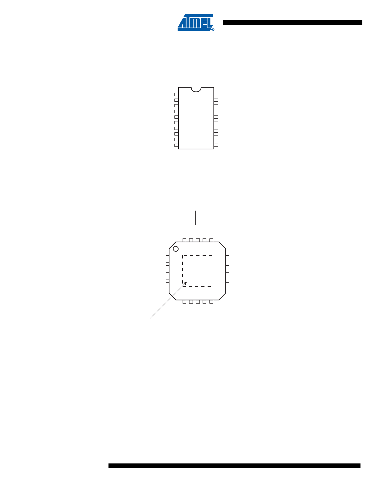
1. Pin Configurations
Figure 1-1. Pinout of ATtiny43U
SOIC
(T0/PCINT8) PB0
(OC0A/PCINT9) PB1
(OC0B/PCINT10) PB2
(T1/CLKO/PCINT11) PB3
(DI/OC1A/PCINT12) PB4
(DO/OC1B/PCINT13) PB5
(USCK/SCL/PCINT14) PB6
(INT0/PCINT15) PB7
QFN/MLF Top View
(OC0B/PCINT9) PB2
(T1/CLKO/PCINT11) PB3
(DI/OC1A/PCINT12) PB4
(DO/OC1B/PCINT13) PB5
(USCK/SCL/PCINT14) PB6
VCC
GND
1
2
3
4
5
6
7
8
9
10
1
2
3
4
5
20
19
18
17
16
15
14
13
12
11
(T0/PCINT8)
PB0
PB1 (OC0A/PCINT9)
PA7 (RESET/dW/PCINT7)
PA6 (CLKI)
PA5 (AIN1/PCINT5)
2019181716
PA7 (RESET/dW/PCINT7)
PA6 (CLKI/PCINT6)
PA5 (AIN1/PCINT5)
PA4 (AIN0/PCINT4)
PA3 (ADC3/PCINT3)
PA2 (ADC2/PCINT2)
PA1 (ADC1/PCINT1)
PA0 (ADC0/PCINT0)
VBAT
LSW
15
14
13
12
11
PA4 (AIN0/
PA3 (ADC3/
PA2 (ADC2/
PA1 (ADC1/
PA0 (ADC0/
PCINT4)
PCINT3)
PCINT2)
PCINT1)
PCINT0)
1.1 Pin Descriptions
1.1.1 V
1.1.2 GND
1.1.3 Port A (PA7:PA0)
2
CC
Supply voltage.
Ground.
Port A is a 8-bit bi-directional I/O port with internal pull-up resistors (selected for each bit). The
Port A output buffers have symmetrical drive characteristics with both high sink and source
NOTE: Bottom pad should
be Soldered to ground.
678910
VCC
LSW
GND
VBAT
(INT0/PCINT15) PB7
8048B–AVR–03/09
Page 3

capability except PA7 which has the RESET capability. To use pin PA7 as an I/O pin, instead of
RESET pin, program (‘0’) RSTDISBL fuse. As inputs, Port A pins that are externally pulled low
will source current if the pull-up resistors are activated. The Port A pins are tri-stated when a
reset condition becomes active, even if the cloc k is not ru nn in g.
Port A has an alternate functions as analog inputs for the ADC, analog comparator, timer/counter, SPI and pin change interrupt as described in “Alternate Port Functions” on page 67.
1.1.4
RESET
Reset input. A low level on this pin for longer than the minimum pulse length will generate a
reset, even if the clock is not running. The minimum pulse length is given in Table 20-4 on page
158. Shorter pulses are not guaranteed to gener at e a re se t.
1.1.5 Port B (PB7:PB0)
Port B is a 8-bit bi-directional I/O port with internal pull-up resistors (selected for each bit). The
Port B output buffers have symmetrical drive characteristics with both high sink and source
capability. As inputs, Port B pins that are externally pulled low will source current if the pull-up
resistors are activated. The Port B pins are tri-stated when a reset co ndition becomes active,
even if the clock is not running.
Port B also serves the functions of various special features as listed in Section 11.3 “Alternate
Port Functions” on page 67.
1.1.6 LSW
Boost converter external inductor connection. Connect to ground when boost converter is disabled permanently.
1.1.7 V
BAT
Battery supply voltage. Connect to ground when boost converter is disabled permanently.
8048B–AVR–03/09
3
Page 4
ATtiny43U
2. Overview
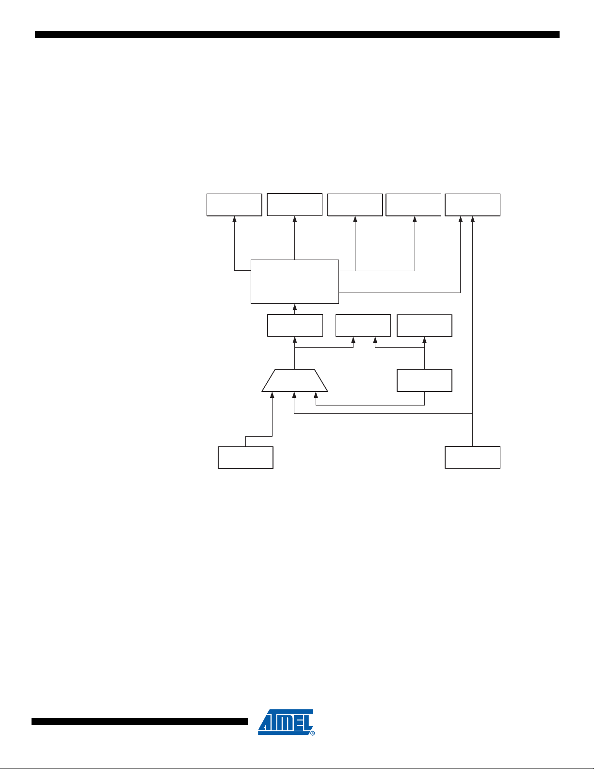
STACK
POINTER
SRAM
PROGRAM
COUNTER
BOOST
CONVERTER
PROGRAMMING
LOGIC
ISP
INTERFACE
INTERNAL
OSCILLATOR
WATCHDOG
TIMER
MCU CONTROL
REGISTER
MCU STATUS
REGISTER
TIMER/
COUNTER0
TIMER/
COUNTER1
CALIBRATED
OSCILLATOR
TIMING AND
CONTROL
INTERRUPT
UNIT
EEPROM
ANALOG
COMPARATOR
ADC
POWER
SUPERVISION
POR
BOD
RESET
ON-CHIP
DEBUG
VOLTAGE
REFERENCE
GENERAL
PURPOSE
REGISTERS
X
Y
Z
ALU
STATUS
REGISTER
PROGRAM
FLASH
INSTRUCTION
REGISTER
INSTRUCTION
DECODER
CONTROL
LINES
DATA REGISTER
PORT A
DIRECTION REG.
PORT A
DRIVERS
PORT A
V
CC
VBAT
LSW
RESET
DATA REGISTER
PORT B
DIRECTION REG.
PORT B
DRIVERS
PORT B
GND
USI
PA7:0 PB7:0
The ATtiny43U is a low-power CMOS 8-bit microcontroller based on the AVR enhanced RISC
architecture. By executing powerful instructions in a single clock cycle, the ATtiny43U achieves
throughputs approaching 1 MIPS pe r MHz allow ing the sy stem de signer to optimize power c onsumption versus processing speed.
Figure 2-1. Block Diagram
4
The AVR core combines a rich instruction set with 32 general purpose working registers. All the
32 registers are directly connected to the Arithmetic Logic Unit (ALU), allowing two independent
registers to be accessed in one single instruction executed in one clock cycle. The resulting
8048B–AVR–03/09
Page 5

architecture is more code efficient while achieving throughputs up to ten times faster than conventional CISC microcontrollers.
The ATtiny43U provides the following features: 4K by te of In-System Programmab le Flash, 64
bytes EEPROM, 256 bytes SRAM, 16 general purpose I/O lines, 32 general purpose working
registers, two 8-bit Timer/Counters with two PWM channels, Internal and External Interrupts, a
4-channel 10-bit ADC, Universal Serial Interface, a programmable Watchdog Timer with internal
Oscillator, internal calibrated oscillator, and three software selectable power saving modes. The
Idle mode stops the CPU while allowing the SRAM, Timer/Counter, ADC, Analog Comparator,
and Interrupt system to continue functioning. The Power-down mode saves the register contents, disabling all chip functions until the next Interrupt or Hardware Reset. The ADC Noise
Reduction mode stops the CPU and all I/O modules except ADC, to minimize switching noise
during ADC conversions.
A special feature of ATtiny43U is the built-in boost voltage converter, which provides 3V supply
voltage from an external, low voltage.
The device is manufactured using Atmel’s high density non-volatile memory technology. The
On-chip ISP Flash allows the Program memory to be re-programmed In-System through an SPI
serial interface, by a conventional non-volatile memory programmer or by an On-chip boot code
running on the AVR core.
The ATtiny43U AVR is supported by a full suite of program and system development tools
including: C Compilers, Macro Assemblers, Program Debugger/Simulators, In-Circuit Emulators,
and Evaluation kits.
8048B–AVR–03/09
5
Page 6

ATtiny43U
3. About
3.1 Resources
A comprehensive set of development tools, drivers and application notes, and datasheets are
available for download on http://www.atmel.com/avr.
3.2 Code Examples
This documentation contains simple code examples t hat brief ly show h ow to us e various parts of
the device. These code examples assume that the part specific header file is included b efore
compilation. Be aware that not all C compiler vendors include bit definitions in the header files
and interrupt handling in C is compiler dependent . Please con firm wit h the C com piler d ocume ntation for more details.
For I/O Registers located in extended I/O map, “IN”, “OUT”, “SBIS”, “SBIC”, “CBI”, and “SBI”
instructions must be replaced with instructions that allow access to extended I/O. Typically
“LDS” and “STS” combined with “SBRS”, “SBRC”, “SBR”, and “CBR”.
3.3 Data Retention
Reliability Qualification results show that the projected data retention failure rate is much less
than 1 PPM over 20 years at 85°C or 100 years at 25°C.
3.4 Disclaimer
Typical values contained in this data sheet are based on simulations and characterization of
other AVR microcontrollers manufactured on the same process technology. Min and Max values will be available after the device is characterized.
6
8048B–AVR–03/09
Page 7
4. AVR CPU Core
Flash
Program
Memory
Instruction
Register
Instruction
Decoder
Program
Counter
Control Lines
32 x 8
General
Purpose
Registrers
ALU
Status
and Control
I/O Lines
EEPROM
Data Bus 8-bit
Data
SRAM
Direct Addressing
Indirect Addressing
Interrupt
Unit
Watchdog
Timer
Analog
Comparator
Timer/Counter 0
Timer/Counter 1
Universal
Serial Interface
4.1 Introduction
This section discusses the AVR core architecture in general. The main function of the CPU core
is to ensure correct program execution. The CPU must therefore be able to access memories,
perform calculations, control peripherals, and handle interrupts.
4.2 Architectural Overview
Figure 4-1. Block Diagram of the AVR Architecture
In order to maximize performance and parallelism, the AVR uses a Harvard architecture – with
separate memories and buses for program and data. Instructions in the Program memory are
executed with a single level pipelining. While one instruction is being executed, the next instruction is pre-fetched from the Program memo ry. This concept enables instructions to be executed
in every clock cycle. The Program memory is In-System Reprogrammable Flash memory.
8048B–AVR–03/09
7
Page 8

ATtiny43U
The fast-access Register File contains 32 x 8-bit general purpose working registers with a single
clock cycle access time. This allows single-cycle Arithmetic Logic Unit (ALU) operation. In a typical ALU operation, two operands are output from the Register File, the operation is executed,
and the result is stored back in the Register File – in one clock cycle.
Six of the 32 registers can be used as three 16-bit indirect address register pointers for Data
Space addressing – enabling efficient address calculations. One of the these address pointe rs
can also be used as an address pointer for look up tables in Flash Program memory. These
added function registers are the 16-bit X-, Y-, and Z-register, described later in this section.
The ALU supports arithmetic and logic operations between registers or between a constant and
a register. Single register operations can also be executed in the AL U. After an arith metic operation, the Status Register is updated to reflect informat ion about the result of the operation.
Program flow is provided by conditional and unconditional jump and call instructions, able to
directly address the whole address space. Most AVR instructions have a single 16-bit word format. Every Program memory address contains a 16- or 32-bit instruction.
During interrupts and subroutine calls, the return address Prog ram Counter (PC) is stored on the
Stack. The Stack is effectively allocated in the general data SRAM, and consequently the Stack
size is only limited by the total SRAM size and the usage of the SRAM. All user programs must
initialize the SP in the Reset routine (before subroutines or interrupts are executed). The Stack
Pointer (SP) is read/write accessible in the I/O space. The data SRAM can easily be accessed
through the five different addressing modes supported in the AVR architecture.
The memory spaces in the AVR architecture are all linear and regular memory maps.
A flexible interrupt module has its control registers in the I/O space with an additional Global
Interrupt Enable bit in the Status Register. All interrupts have a separate Interrupt Vector in the
Interrupt Vector table. The interrupts have priority in accordance with their Interrupt Vector position. The lower the Interrupt Vector address, the higher the priority.
The I/O memory space contains 64 addresses for CPU peripheral functions as Control Registers, SPI, and other I/O functions. The I/O memory can be acces sed directly, or as the Data
Space locations following those of the Register File, 0x20 - 0x5F.
4.3 ALU – Arithmetic Logic Unit
The high-performance AVR ALU operates in direct connection with all the 32 general purpose
working registers. Within a single clock cycle, arithmetic operations between general purpose
registers or between a register and an immediate are execut ed . The ALU ope ra tio ns are divided
into three main categories – arithmetic, logical, and bit-functions. Some implementations of the
architecture also provide a powerful multiplier supporting both signed/unsigned multiplication
and fractional format. See the “Instruction Set” section for a detailed description.
4.4 Status Register
The Status Register contains information abou t th e result o f th e most r ecently exe cuted arith metic instruction. This information can be used for altering program flow in order to perform
conditional operations. Note that the Status Register is updated after all ALU operations, as
specified in the Instruction Set Refe rence. This wil l in many cases remove the n eed for using the
dedicated compare instructions, resulting in faster and more compact code.
8
The Status Register is not automatically stored when entering an interrupt routine and restored
when returning from an interrupt. This must be hand le d by so ftware.
8048B–AVR–03/09
Page 9

4.4.1 SREG - AVR Status Register
Bit 76543210
0x3F (0x5F) I T H S V N Z C SREG
Read/Write R/W R/W R/W R/W R/W R/W R/W R/W
Initial Value00000000
• Bit 7 – I: Global Interrupt Enable
The Global Interrupt Enable bit must be set for the interrupts to be enabled. The individual interrupt enable control is then performed in separate control registers. If the Global Interrupt Enable
Register is cleared, none of the interrupts are enabled independent of the individual interrupt
enable settings. The I-bit is cleared by hardware after an interrupt has occurred, and is set by
the RETI instruction to enable subsequent interrupts. The I-bit can also be set and cleared by
the application with the SEI and CLI instructions, as described in the instruction set reference.
• Bit 6 – T: Bit Copy Storage
The Bit Copy instructions BLD (Bit LoaD) and BST (Bit STore) use the T-bit as source or destination for the operated bit. A bit from a register in the Register File can be copied into T by the
BST instruction, and a bit in T can be copied into a bit in a register in the Register File by the
BLD instruction.
• Bit 5 – H: Half Carry Flag
The Half Carry Flag H indicates a Half Carry in some arithmetic operations. Half Carry is useful
in BCD arithmetic. See the “Instruction Set Description” for detailed information.
• Bit 4 – S: Sign Bit, S = N
⊕ V
The S-bit is always an exclusive or between the Negative Flag N and the Two’s Complement
Overflow Flag V. See the “Instruction Set Description” for detailed information.
• Bit 3 – V: Two’s Complement Overflow Flag
The Two’s Complement Overflow Flag V supports two’s complement arithmetics. See the
“Instruction Set Description” for detailed information.
• Bit 2 – N: Negative Flag
The Negative Flag N indicates a negative result in an arithmetic or logic operation. See the
“Instruction Set Description” for detailed information.
• Bit 1 – Z: Zero Flag
The Zero Flag Z indicates a zero result in an arithmetic or logic operation. See the “Instruction
Set Description” for detailed information.
• Bit 0 – C: Carry Flag
The Carry Flag C indicates a carry in an arithmetic or logic operation. See the “Instruction Set
Description” for detailed information.
8048B–AVR–03/09
9
Page 10

ATtiny43U
4.5 General Purpose Register File
The Register File is optimized for the AVR Enhanced RISC instruction set. In order t o achieve
the required performance and flexibility, the following input/output schemes are supported by the
Register File:
• One 8-bit output operand and one 8-bit result input
• Two 8-bit output operands and one 8-bit result input
• Two 8-bit output operands and one 16-bit result input
• One 16-bit output operand and one 16-bit result input
Figure 4-2 on page 10 shows the structure of the 32 general purpose working registers in the
CPU.
Figure 4-2. AVR CPU General Purpose Working Registers
General R14 0x0E
Purpose R15 0x0F
Working R16 0x10
Registers R17 0x11
7 0 Addr.
R0 0x00
R1 0x01
R2 0x02
…
R13 0x0D
…
R26 0x1A X-register Low Byte
R27 0x1B X-register High Byte
R28 0x1C Y-register Low Byte
R29 0x1D Y-register High Byte
R30 0x1E Z-register Low Byte
R31 0x1F Z-register High Byte
4.5.1 The X-register, Y-register, and Z-register
10
Most of the instructions operating on the Register File have direct access to all registers, and
most of them are single cycle instructions.
As shown in Figure 4-2, each register is also assigned a Data memory address, mapping them
directly into the first 32 locations of the user Data Space. Although not being physically implemented as SRAM locations, this memory organization provides great flexibility in access of the
registers, as the X-, Y- and Z-pointer registers can be set to index any register in the file.
The registers R26..R31 have some added functions to their general purpose usage. These registers are 16-bit address pointers for indirect addressing of the data space. The three indirect
address registers X, Y, and Z are defined as described in Figure 4-3 on page 11.
8048B–AVR–03/09
Page 11
4.6 Stack Pointer
Figure 4-3. The X-, Y-, and Z-registers
15 XH XL 0
X-register 707 0
R27 (0x1B) R26 (0x1A)
15 YH YL 0
Y-register 707 0
R29 (0x1D) R28 (0x1C)
15 ZH ZL 0
Z-register 7070
R31 (0x1F) R30 (0x1E)
In the different addressing modes these addr ess regist er s have fun cti ons a s fi xed d isp lacement ,
automatic increment, and automatic decrement (see the instruction set reference for details).
The Stack is mainly used for storing temporary data, for storing local variables and for storing
return addresses after interrupts and subroutine calls. Note that the Stack is implemented as
growing from higher to lower memory locations. The Stack Pointer Register always points to the
top of the Stack. The Stack Pointer points to the data SRAM Stack area wh ere the Subroutine
and Interrupt Stacks are located. A Stack PUSH command will decrease the Stack Pointer.
The Stack in the data SRAM must be defined by the program before any subroutine calls ar e
executed or interrupts are enabled. Initial Stack Pointer value equa ls the last address of the
internal SRAM and the Stack Pointer must be set to point above start of the SRAM, see Figure
5-2 on page 16.
See Table 4-1 for Stack Pointer details.
Table 4-1. Stack Pointer instructions
Instruction Stack pointer Description
PUSH Decremented by 1 Data is pushed onto the stack
CALL
ICALL
RCALL
POP Incremented by 1 Data is popped from the stack
RET
RETI
Decremented by 2
Incremented by 2 Return address is popped from the stack with return from
Return address is pushed onto the stack with a subroutine call or
interrupt
subroutine or return from interrupt
The AVR Stack Pointer is implemented as two 8-bit registers in the I/O space. The number of
bits actually used is implementation dependent. Note that the data space in some implementations of the AVR architecture is so small that only SPL is needed. In this case, the SPH Register
will not be present.
8048B–AVR–03/09
11
Page 12
ATtiny43U
4.6.1 SPH and SPL — Stack Pointer Register
clk
1st Instruction Fetch
1st Instruction Execute
2nd Instruction Fetch
2nd Instruction Execute
3rd Instruction Fetch
3rd Instruction Execute
4th Instruction Fetch
T1 T2 T3 T4
CPU
Total Execution Time
Register Operands Fetch
ALU Operation Execute
Result Write Back
T1 T2 T3 T4
clk
CPU
Bit 151413121110 9 8
0x3E (0x5E) SP15 SP14 SP13 SP12 SP11 SP10 SP9 SP8 SPH
0x3D (0x5D) SP7 SP6 SP5 SP4 SP3 SP2 SP1 SP0 SPL
76543210
Read/Write R/W R/W R/W R/W R/W R/W R/W R/W
Read/Write R/W R/W R/W R/W R/W R/W R/W R/W
Initial Value
Initial Value
RAMEND RAMEND RAMEND RAMEND RAMEND RAMEND RAMEND RAMEND
RAMEND RAMEND RAMEND RAMEND RAMEND RAMEND RAMEND RAMEND
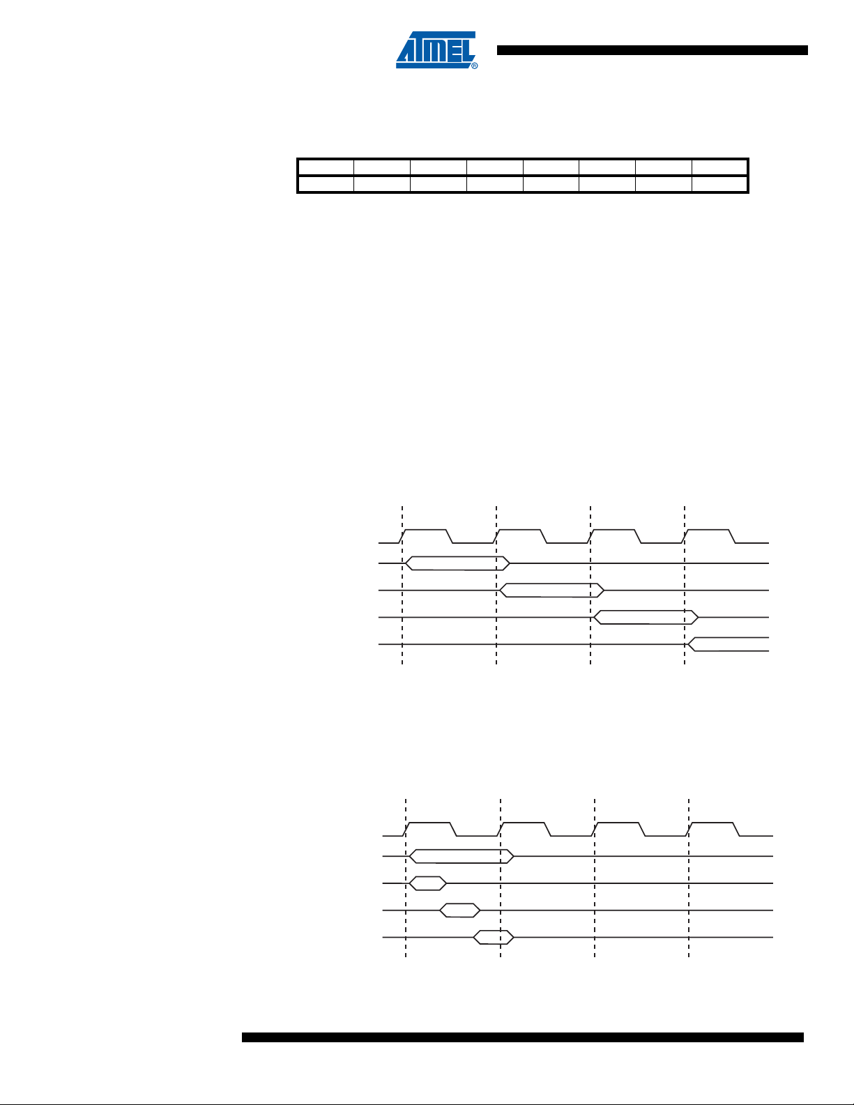
4.7 Instruction Execution Timing
This section describes the general access timing concepts for instruction execution. The AVR
CPU is driven by the CPU clock clk
chip. No internal clock division is used.
Figure 4-4 on page 12 shows the parallel instruction fetches and instruction executions enabled
by the Harvard architecture and the fast access Register File concept. This is the basic pipelining concept to obtain up to 1 MIPS per MH z with the correspo nding unique results for function s
per cost, functions per clocks, and functions per power-unit.
Figure 4-4. The Parallel Instruction Fetches and Instruction Executions
, directly generated from the selected clock source for the
CPU
12
Figure 4-5 on page 12 shows the internal timing concept for the Register File. In a single clock
cycle an ALU operation using two register operands is executed, and the result is stored back to
the destination register.
Figure 4-5. Single Cycle ALU Operation
8048B–AVR–03/09
Page 13

4.8 Reset and Interrupt Handling
The AVR provides several different interrupt sources. These interrupts and the separate Reset
Vector each have a separate Program Vector in the Program memory space. All interrupts are
assigned individual enable bits which must be written logic one toge ther with the Glo bal Interru pt
Enable bit in the Status Register in order to enable the int errupt.
The lowest addresses in the Program memory space are by default defined as the Reset and
Interrupt Vectors. The complete list of vectors is shown in “Interrupts” on page 57. The list also
determines the priority levels of the different interrupts. The lower the address the higher is the
priority level. RESET has the highest priority, and next is INT0 – the External Interrupt Request
0.
When an interrupt occurs, the Global Interrupt Enable I-bit is cleared and all interrupts are dis-
abled. The user software can write logic one to the I-bit to enable nested interrupts. All enabled
interrupts can then interrupt the current interrupt routine. The I-bit is automatically set when a
Return from Interrupt instruction – RETI – is executed.
There are basically two types of interrupts. The first type is triggered by an event that sets the
Interrupt Flag. For these interrupts, the Program Counter is vectored to the actual Interrupt Vector in order to execute the interrupt handling routine, and hardware clears the corresponding
Interrupt Flag. Interrupt Flags can also be cleared by writing a logic one to the fl ag bit position(s)
to be cleared. If an interrupt condition occurs while the corresponding interrupt enable bit is
cleared, the Interrupt Flag will be set and remembered until the interrupt is enabled, or the flag is
cleared by software. Similarly, if one or more interrupt conditions occur while the Global Interrupt
Enable bit is cleared, the corresponding Interrupt Flag(s) will be set and remembered until the
Global Interrupt Enable bit is set, and will then be executed by order of priority.
The second type of interrupts will trigger as long as the interrupt condition is present. These
interrupts do not necessarily have Int errupt Flags. If the interrup t condition disappears before t he
interrupt is enabled, the interrupt will not be triggered.
When the AVR exits from an interrupt, it will always return to the main program and execute one
more instruction before any pending interrupt is served.
Note that the Status Register is not automatically stored when entering an interrupt routine, nor
restored when returning from an interrupt rou tine. This must be handled by software.
When using the CLI instruction to disable interrupts, the interrupts will be immediately disabled.
No interrupt will be executed after the CLI instruction, even if it occurs simultaneously with the
CLI instruction. The following example shows how this can be used to avoid interrupts during the
timed EEPROM write sequence.
8048B–AVR–03/09
13
Page 14

ATtiny43U
Assembly Code Example
in r16, SREG ; store SREG value
cli ; disable interrupts during timed sequence
sbi EECR, EEMPE ; start EEPROM write
sbi EECR, EEPE
out SREG, r16 ; restore SREG value (I-bit)
C Code Example
char cSREG;
cSREG = SREG; /* store SREG value */
/* disable interrupts during timed sequence */
_CLI();
EECR |= (1<<EEMPE); /* start EEPROM write */
EECR |= (1<<EEPE);
SREG = cSREG; /* restore SREG value (I-bit) */
When using the SEI instruction to enable interrupts, the instruction following SEI will be executed before any pending interrupts, as shown in this example.
Assembly Code Example
sei ; set Global Interrupt Enable
sleep; enter sleep, waiting for interrupt
; note: will enter sleep before any pending
; interrupt(s)
C Code Example
_SEI(); /* set Global Interrupt Enable */
_SLEEP(); /* enter sleep, waiting for interrupt */
/* note: will enter sleep before any pending interrupt(s) */
4.8.1 Interrupt Response Time
The interrupt execution response for all the enabled AVR interrupts is four clock cycles minimum. After four clock cycles the Program Vector address for the a ctual interru pt handling routine
is executed. During this four clock cycle period, the Program Counter is pushed onto the Stack.
The vector is normally a jump to the interrupt routine, and this jump takes three clock cycles. If
an interrupt occurs during execution of a multi-cycle instruction, this instruction is completed
before the interrupt is served. If an interrupt occurs when the MCU is in sleep mode, the interrupt
execution response time is increased by four clock cycles. This increase comes in ad dition to the
start-up time from the selected sleep mode.
A return from an interrupt handling routine takes four clock cycles. During these four clock
cycles, the Program Counter (two bytes) is popped back from the Stack, the Stack Pointer is
incremented by two, and the I-bit in SREG is set.
14
8048B–AVR–03/09
Page 15

5. Memories
5.1 Overview
This section describes the different memories in ATt iny43U. The AVR architect ure ha s t wo main
memory spaces, the Data memory and the Program memory space. In addition, the ATtiny43U
features an EEPROM Memory for data storage. All three memory spaces are linear and regular.
5.2 In-System Re-programmable Flash Program Memory
The ATtiny43U contains 4K byte On-chip In-System Reprogrammable Flash memory for program storage. Since all AVR instructions are 16 or 32 bits wide, the Flash is or ganized as 204 8 x
16.
The Flash memory has an endurance of at least 10,000 write/erase cycles. The ATtiny43U Pro-
gram Counter (PC) is 11 bits wide, thus addressing the 2048 Program memory locations.
“Memory Programming” on page 139 contains a detailed description on Flash data downloading.
Constant tables can be allocated within the entire Prog ram memory address space (se e the
LPM – Load Program memory instruction description).
Timing diagrams for instruction fetch and execution are presented in “Instruction Execution Tim-
ing” on page 12.
Figure 5-1. Program Memory Map
5.3 SRAM Data Memory
Figure 5-2 on page 16 shows how the ATtiny43U SRAM Memory is organized.
The low Data memory locations address both the Register File, the I/O memory and the internal
data SRAM, as follows:
• The first 32 locations address the Register File
• The next 64 locations address the standard I/O memory
• The last 256 locations address the internal data SRAM
Program Memory
0x0000
0x07FF
8048B–AVR–03/09
The five different addressing modes for the Data memory cover: Dire ct, Indirect with Displacement, Indirect, Indirect with Pre-decrement, and Indirect with Post-increment. In the Register
File, registers R26 to R31 feature the indirect addressing pointer registers.
15
Page 16
ATtiny43U
The direct addressing reaches the entire data space.
clk
WR
RD
Data
Data
Address
Address valid
T1 T2 T3
Compute Address
Read
Write
CPU
Memory Access Instruction
Next Instruction
The Indirect with Displacement mode reaches 63 address locations f rom the base address given
by the Y- or Z-register.
When using register indirect addressing modes with automatic pre-decrement and post-increment, the address registers X, Y, and Z are decremented or incremented.
The 32 general purpose working registers, 64 I/O Registers, and the 256 bytes of internal data
SRAM in ATtiny43U are all accessible through all these addressing modes. The Register File is
described in “General Purpose Register File” on page 10.
Figure 5-2. Data Memory Map
Data Memory
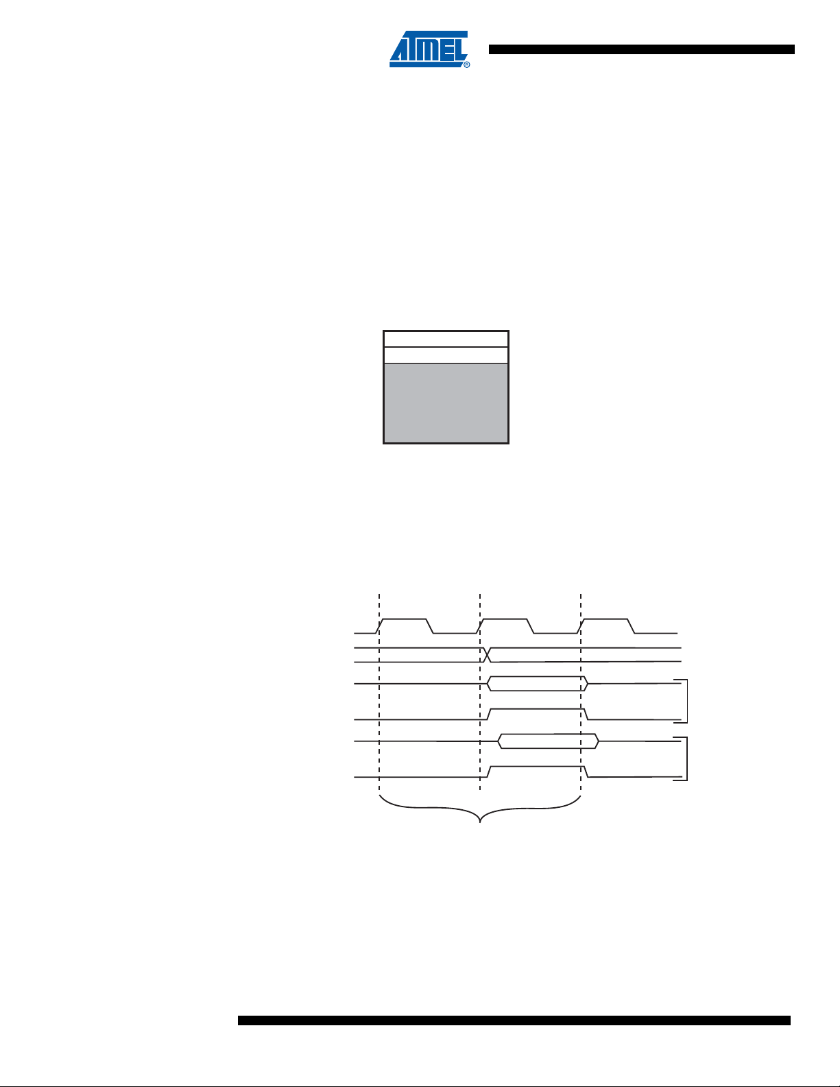
5.3.1 Data Memory Access Times
This section describes the general access timing concepts for internal memory access. The
internal data SRAM access is performed in tw o clk
16.
Figure 5-3. On-chip Data SRAM Access Cycles
32 Registers
64 I/O Registers
Internal SRAM
(256 x 8)
0x0000 - 0x001F
0x0020 - 0x005F
0x0060
0x15F
cycles as described in Figure 5-3 on page
CPU
5.4 EEPROM Data Memory
16
The ATtiny43U contains 64 bytes of data EEPROM memory. It is organized as a separate data
space, in which single bytes can be read and written. The EEPROM has an endurance of at
least 100,000 write/erase cycles. The access between the EEPROM and the CPU is described
in the following, specifying the EEPROM Address Registers, the EEPROM Data Register, and
8048B–AVR–03/09
Page 17

the EEPROM Control Register. For a detailed description of Serial data downloading to the
EEPROM, see “Serial Programming” on page 151.
5.4.1 EEPROM Read/Write Access
The EEPROM Access Registers are accessible in the I/O space.
The write access times for the EEPROM are given in Table 5-1 on page 21. A self-timing func-
tion, however, lets the user software detect when the next byte can be written. If the user code
contains instructions that write the EEPROM, some precautions must be taken. In heavily filtered power supplies, V
device for some period of time to run at a voltage lower than specified as minimum for the clock
frequency used. See “Preventing EEPROM Corruption” on page 19 for details on how to avoid
problems in these situations.
In order to prevent unintentional EEPROM writes, a specific write procedure must be followed.
See “Atomic Byte Programming” on page 17 and “Split Byte Programming” on page 17 for
details on this.
When the EEPROM is read, the CPU is halted for four clock cycles before the next instruction is
executed. When the EEPROM is written, the CPU is halted for two clock cycles before the next
instruction is executed.
5.4.2 Atomic Byte Programming
Using Atomic Byte Programming is the simplest mode. When writing a byte to the EEPROM, the
user must write the address into the EEAR Register and data into EEDR Register. If the EEPMn
bits are zero, writing EEPE (within four cycles after EEMPE is written) will trigger the erase/write
operation. Both the erase and write cycle are done in one operation and the total programming
time is given in Table 1. The EEPE bit remains set until the erase and write operations are completed. While the device is busy with programming, it is not possible to do any other EEPROM
operations.
is likely to rise or fall slowly on Power-up/down. This causes the
CC
5.4.3 Split Byte Programming
It is possible to split the erase and write cycle in two different operations. This may be useful if
the system requires short access time for some limited period of time (typically if the power supply voltage falls). In order to take advantage of this method, it is required that the locations to be
written have been erased before the write operation. But since the erase and write operations
are split, it is possible to do the erase operations whe n the system allows doing time-critical
operations (typically after Power-up).
5.4.4 Erase
To erase a byte, the address must be written to EEAR. If the EEPMn bits are 0b01, writing the
EEPE (within four cycles after EEMPE is written) will trigger the erase operation only (programming time is given in Table 1). The EEPE bit remains set until the erase operation completes.
While the device is busy programming, it is not possible to do any other EEPROM operations.
5.4.5 Write
To write a location, the user must write the address into EEAR and the data into EEDR. If the
EEPMn bits are 0b10, writing the EEPE (within four cycles after EEMPE is written) will trigger
the write operation only (programming time is given in Table 1). The EEPE bit remains set until
the write operation completes. If the location to be written has not been erased before write, the
8048B–AVR–03/09
17
Page 18

ATtiny43U
data that is stored must be considered as lost. While the device is busy with programming, it is
not possible to do any other EEPROM operations.
The calibrated Oscillator is used to time the EEPROM accesses. Make sure the Oscillator frequency is within the requirements described in “OSCCAL – Oscillator Calibration Register” on
page 28.
The following code examples show one assembly and one C function for erase, write, or atomic
write of the EEPROM. The examples assume that interrupts are controlled (e.g., by disabling
interrupts globally) so that no interrupts will occur during execution of these functions.
Assembly Code Example
EEPROM_write:
; Wait for completion of previous write
sbic EECR,EEPE
rjmp EEPROM_write
; Set Programming mode
ldi r16, (0<<EEPM1)|(0<<EEPM0)
out EECR, r16
; Set up address (r17) in address register
out EEAR, r17
; Write data (r19) to data register
out EEDR,r19
; Write logical one to EEMPE
sbi EECR,EEMPE
; Start eeprom write by setting EEPE
sbi EECR,EEPE
ret
18
C Code Example
void EEPROM_write(unsigned char ucAddress, unsigned char ucData)
{
/* Wait for completion of previous write */
while(EECR & (1<<EEPE))
;
/* Set Programming mode */
EECR = (0<<EEPM1)|(0<<EEPM0)
/* Set up address and data registers */
EEAR = ucAddress;
EEDR = ucData;
/* Write logical one to EEMPE */
EECR |= (1<<EEMPE);
/* Start eeprom write by setting EEPE */
EECR |= (1<<EEPE);
}
8048B–AVR–03/09
Page 19

The next code examples show assembly and C functions for reading the EEPROM. The examples assume that interrupts are controlled so that no interrupts will occur during execution of
these functions.
Assembly Code Example
EEPROM_read:
; Wait for completion of previous write
sbic EECR,EEPE
rjmp EEPROM_read
; Set up address (r17) in address register
out EEAR, r17
; Start eeprom read by writing EERE
sbi EECR,EERE
; Read data from data register
in r16,EEDR
ret
C Code Example
unsigned char EEPROM_read(unsigned char ucAddress)
{
/* Wait for completion of previous write */
while(EECR & (1<<EEPE))
;
/* Set up address register */
EEAR = ucAddress;
/* Start eeprom read by writing EERE */
EECR |= (1<<EERE);
/* Return data from data register */
return EEDR;
}
5.4.6 Preventing EEPROM Corruption
During periods of low V
too low for the CPU and the EEPROM to operate properly. These issues a re the same as for
board level systems using EEPROM, and the same design solutions should be applied.
An EEPROM data corruption can be caused by two situations when the voltage is too low. First,
a regular write sequence to the EEPROM requires a minimum voltage to operate correctly. Secondly, the CPU itself can execute instructions incorrectly, if the supply voltage is too low.
EEPROM data corruption can easily be avoided by following this design recommendation:
Keep the AVR RESET active (low) during periods of insufficient power supply voltage. This can
be done by enabling the internal Brown-out Detector (BOD). If the detection level of the internal
BOD does not match the needed detection level, an external low V
be used. If a reset occurs while a write operation is in progress, the write operation will be completed provided that the power supply voltage is sufficient.
8048B–AVR–03/09
, the EEPROM data can be corrupted because the supply voltage is
CC
reset protection circuit can
CC
19
Page 20

ATtiny43U
5.5 I/O Memory
The I/O space definition of the ATtiny43U is shown in “Register Summary” on page 167.
All I/Os and peripherals are placed in the I/O space. All I/O locations may be accessed by the
LD/LDS/LDD and ST/STS/STD instructions, transferring data between the 32 general purpose
working registers and the I/O space. I/O Registers within the address range 0x00 - 0x1F are
directly bit-accessible using the SBI and CBI instructions. In these registers, the value of single
bits can be checked by using the SBIS and SBIC instruct ion s. See th e instr uc tion se t section for
more details. When using the I/O sp ecific commands IN and O UT, the I/O addresses 0x00 0x3F must be used. When addressing I/O Registers as data space using LD and ST instructions, 0x20 must be added to these addresses.
For compatibility with future devices, reserved bits should be written to zero if accessed.
Reserved I/O memory addresses should never be written.
Some of the Status Flags are cleared by writing a logical one to them. Note that, unlike most
other AVRs, the CBI and SBI instructions will only operate on the specified bit, and can therefore
be used on registers containing such Status Flags. The CBI and SBI instructions work with registers 0x00 to 0x1F only.
The I/O and Peripherals Control Registers are explained in later sections.
5.5.1 General Purpose I/O Registers
ATtiny43U contains three General Purpose I/O Registers. These registers can be used for storing any information, and they are particularly useful for storing global variables and status flags.
General Purpose I/O Registers within the address range 0x00 - 0x1F are directly bit-accessible
using the SBI, CBI, SBIS, and SBIC instructions.
5.6 Register Description
5.6.1 EEAR – EEPROM Address Register
Bit 76543210
0x1E (0x3E) - - EEAR5 EEAR4 EEAR3 EEAR2 EEAR1 EEAR0 EEAR
Read/Write R R R/W R/W R/W R/W R/W R/W
Initial Value 0 0 X X X X X X
• Bits 7:6 – Res: Reserved Bit
These bits are reserved and will always read zero.
• Bits 5:0 – EEAR[5:0]: EEPROM Address
The EEPROM Address Register – EEAR – specifies the EEPROM address. The EEPROM data
bytes are addressed linearly in the range 0...(64-1). The initial value of EEAR is undefined. A
proper value must be written before the EEPROM may be accessed.
20
8048B–AVR–03/09
Page 21
5.6.2 EEDR – EEPROM Data Register
Bit 76543210
0x1D (0x3D) EEDR7 EEDR6 EEDR5 EEDR4 EEDR3 EEDR2 EEDR1 EEDR0 EEDR
Read/Write R/W R/W R/W R/W R/W R/W R/W R/W
Initial Value 0 0 0 0 0 0 0 0
• Bits 7:0 – EEDR[7:0]: EEPROM Data
For the EEPROM write operation the EEDR Register contains the data to be written to the
EEPROM in the address given by the EEAR Register. For the EEPROM read operation, the
EEDR contains the data read out from the EEPROM at the address given by EEAR.
5.6.3 EECR – EEPROM Control Register
Bit 76543210
0x1C (0x3C) – – EEPM1 EEPM0 EERIE EEMPE EEPE EERE EECR
Read/Write R R R/W R/W R/W R/W R/W R/W
Initial Value 0 0 X X 0 0 X 0
• Bit 7 – Res: Reserved Bit
These bits are reserved and will always read zero. For compatibility with future AVR devic es,
always write this bit to zero. After reading, mask out this bit.
• Bit 6 – Res: Reserved Bit
These bits are reserved and will always read zero.
• Bits 5, 4 – EEPM1 and EEPM0: EEPROM Mode Bits
The EEPROM Programming mode bits setting defines which programming action that will be
triggered when writing EEPE. It is possible to program data in on e atomic operation (e rase the
old value and program the new value) or to split the Erase and Write operations in two different
operations. The Programming t imes fo r the d ifferen t modes ar e shown in Table 5- 1. While EEPE
is set, any write to EEPMn will be ignored. During reset, the EEPMn bits will be reset to 0b00
unless the EEPROM is busy programming.
Table 5-1. EEPROM Mode Bits
Programming
EEPM1 EEPM0
0 0 3.4 ms Erase and Write in one operation (Atomic Operation)
0 1 1.8 ms Erase Only
1 0 1.8 ms Write Only
1 1 – Reserved for future use
Time Operation
• Bit 3 – EERIE: EEPROM Ready Interrupt Enable
Writing EERIE to one enables the EEPROM Ready Interrupt if the I-bit in SREG is set. Writing
EERIE to zero disables the interrupt. The EEPROM Ready Interrupt generates a constant interrupt when Non-volatile memory is ready for programming.
• Bit 2 – EEMPE: EEPROM Master Program Enable
The EEMPE bit determines whether writing EEPE to one will have effect or not.
8048B–AVR–03/09
21
Page 22

ATtiny43U
When EEMPE is set, setting EEPE within four clock cycles will program the EEPROM at the
selected address. If EEMPE is zero, setting EEPE will have no effect. When EEMPE has been
written to one by software, hardware clears the bit to zero after four clock cycles.
• Bit 1 – EEPE: EEPROM Program Enable
The EEPROM Program Enable Signal EEPE is the programming enable signal to the EEPROM.
When EEPE is written, the EEPROM will be programmed according to the EEPMn bits setting.
The EEMPE bit must be written to one before a logical one is written to EEPE, otherwise no
EEPROM write takes place. When the write access time has elapsed, the EEPE bit is cleared
by hardware. When EEPE has been set, the CPU is halted for two cycles before the next
instruction is executed.
• Bit 0 – EERE: EEPROM Read Enable
The EEPROM Read Enable Signal – EERE – is the read strobe to the EEPROM. When the correct address is set up in the EEAR Register, the EERE bit must be written to one to trigger the
EEPROM read. The EEPROM read access takes one instruction, and the requested data is
available immediately. When the EEPROM is read, the CPU is halted for four cycles before the
next instruction is executed. The user should poll the EEPE bit before starting the read operation. If a write operation is in progress, it is neither possible to read the EEPROM, nor to change
the EEAR Register.
5.6.4 GPIOR2 – General Purpose I/O Regist er 2
Bit 76543210
0x15 (0x35) MSB LSB GPIOR2
Read/Write R/W R/W R/W R/W R/W R/W R/W R/W
Initial Value 0 0 0 0 0 0 0 0
5.6.5 GPIOR1 – General Purpose I/O Regist er 1
Bit 76543210
0x14 (0x34) MSB LSB GPIOR1
Read/Write R/W R/W R/W R/W R/W R/W R/W R/W
Initial Value 0 0 0 0 0 0 0 0
5.6.6 GPIOR0 – General Purpose I/O Regist er 0
Bit 76543210
0x13 (0x33) MSB LSB GPIOR0
Read/Write R/W R/W R/W R/W R/W R/W R/W R/W
Initial Value 0 0 0 0 0 0 0 0
22
8048B–AVR–03/09
Page 23
6. System Clock and Clock Options
6.1 Clock Systems and their Distribution
Figure 6-1 presents the principal clock systems in the AVR and their distribution. All of the clocks
need not be active at a given time. In order to reduce power consump tion, th e cloc ks to modules
not being used can be halted by using different sleep modes, as described in “Power Manage-
ment and Sleep Modes” on page 31. The clock systems are detailed below.
Figure 6-1. Clock Distribution
General I/O
Modules
clk
I/O
External Clock
ADC
clk
AVR Clock
Control Unit
System Clock
Prescaler
Source clock
Clock
Multiplexer
ADC
CPU Core RAM
clk
CPU
clk
FLASH
Reset Logic
Watchdog Timer
Watchdog clock
Watchdog
Oscillator
Flash and
EEPROM
Calibrated RC
Oscillator
6.1.1 CPU Clock – clk
The CPU clock is routed to parts of the system concerned with operation of the AVR core.
Examples of such modules are the General Purpose Register File, the Status Register and the
data memory holding the Stack Pointer. Halting the CPU clock inhibits the core from performing
general operations and calculations.
6.1.2 I/O Clock – clk
I/O
The I/O clock is used by the majority of the I/O modules, like Timer/Counters. The I/O clock is
also used by the External Interrupt module, but note that some external interrupts are detected
by asynchronous logic, allowing such interrupts to b e detected even if the I/O clock is halted.
Also note that start condition detection in the USI module is carried out asynchronously when
clk
6.1.3 Flash Clock – clk
The Flash clock controls operation of the Flash inte rface. The Fla sh clock is usually active simultaneously with the CPU clock.
8048B–AVR–03/09
CPU
is halted.
I/O
FLASH
23
Page 24
ATtiny43U
6.1.4 ADC Clock – clk
EXTERNAL
CLOCK
SIGNAL
CLKI
GND
6.2 Clock Sources
ADC
The ADC is provided with a dedicated clock domain. This allows halting the CPU and I/O clocks
in order to reduce noise generated by digital cir cuit ry. Th is gives mo re accurat e ADC conversion
results.
The device has the following clock source options, selec table by Flash Fuse bits as shown
below. The clock from the selected so ur ce is i npu t to th e AVR clo c k gene ra to r, and r ou te d to t he
appropriate modules.
6.2.1 External Clock
Table 6-1. Device Clocking Options Select
Device Clocking Option CKSEL3..0
External Clock (see page 24) 0000
Calibrated Internal 8 MHz Oscillator (see page 25) 0010
Internal 128 kHz Oscillator (see page 26) 0011
Reserved 0001, 0100-1111
Note: 1. For all fuses “1” means unprogrammed while “0” means programmed.
To drive the device from an external clock source, CLKI should be driven as shown in Figure 6-2
on page 24. To run the device on an external clock, the CKSEL Fuses must be programmed to
“0000” (see Table 6-2).
Table 6-2. Crystal Oscillator Clock Frequency
CKSEL3..0 Frequency
0000 0 - 8 MHz
Figure 6-2. External Clock Drive Configuration
(1)
24
8048B–AVR–03/09
Page 25
When this clock source is selected, start-up times are determined by SUT Fuses as shown in
Table 6-3.
Table 6-3. Start-up Times for the External Clock Selection
SUT1..0
00 6 CK 14CK BOD enabled
01 6 CK 14CK + 4 ms Fast rising power
10 6 CK 14CK + 64 ms Slowly rising power
11 Reserved
from Power-down
When applying an external clock, it is required to avoid sudden changes in the applied clock frequency to ensure stable operation of the MCU. A variation in frequency of more than 2% from
one clock cycle to the next can lead to unpredictable behavior. If changes of more than 2% is
required, ensure that the MCU is kept in Reset during the changes.
Note that the System Clock Prescaler can be used to implement run-ti me changes of the int ernal
clock frequency while still ensuring stable operation. Refer to “Power Management and Sleep
Modes” on page 31 for details.
6.2.2 Calibrated Internal 8 MHz Oscillator
By default, the Internal RC Oscillator provides an approximate 8.0 MHz clock. Though voltage
and temperature dependent, this clock can be very accurately calibrated by the user. See Table
20-2 on page 157 for more details. The device is shipped with the CKDIV8 Fuse programmed.
See “System Clock Prescaler” on page 27 for more details.
Start-up Time
Additional Delay
from Reset Recommended Usage
This clock may be selected as the system cloc k by p rogr am m in g th e CKS E L Fus es a s sh own in
Table 6-4. If selected, it will operate with no external components. During reset, hardware loads
the pre-programmed calibration value into th e OSCCAL Re giste r a nd the reby aut omat ica lly calibrates the RC Oscillator. The accuracy of this calibration is shown as Factory calibration in
Table 20-2 on page 157.
By changing the OSCCAL register from SW, see “OSCCAL – Oscillator Calibration Register” on
page 28, it is possible to get a higher calibration accuracy than by using the factory calibration.
The accuracy of this calibration is shown as User calibration in Table 20-2 on page 157.
When this Oscillator is used as the chip clock, the Watchdog Oscillator will still be used for the
Watchdog Timer and for the Reset Time-out. For more information on the pre-programmed calibration value, see the section “Calibration Byte” on page 142.
Table 6-4. Internal Calibrated RC Oscillator Operating Modes
CKSEL3..0 Nominal Frequency (MHz)
(1)
0010
Notes: 1. The device is shipped with this option selected.
8.0
8048B–AVR–03/09
25
Page 26
ATtiny43U
When this Oscillator is selected, start-up times are determined by the SUT Fuses as shown in
Table 6-5 below.
Table 6-5. Start-up times for Internal Calibrated RC Oscillator Clock Selection
SUT1..0
00 6 CK 14CK
01 6 CK 14CK + 4 ms Fast rising power
(2)
10
11 Reserved
Note: 1. If the RSTDISBL fuse is programmed, this start-up time will be increased to
2. The device is shipped with this option selected.
6.2.3 Internal 128 kHz Oscillator
The 128 kHz internal oscillator is a low power oscillator providing a clock of 128 kHz. The frequency is nominal at 3V and 25°C. This clock may be select as the system clock by
programming the CKSEL Fuses to “11” as shown in Table 6-6 below.
Table 6-6. 128 kHz Internal Oscillator Operating Modes
When this clock source is selected, start-up times are determined by the SUT Fuses as shown in
Table 6-7 below.
Start-up Time
from Power-down
6 CK 14CK + 64 ms Slowly rising power
14CK + 4 ms to ensure programming mode can be entered.
CKSEL3..0 Nominal Frequency
0011 128 kHz
Additional Delay from
Reset (VCC = 5.0V) Recommended Usage
(1)
BOD enabled
Table 6-7. Start-up Times for the 128 kHz Internal Oscillator
SUT1..0
00 6 CK 14CK
01 6 CK 14CK + 4 ms Fast rising power
10 6 CK 14CK + 64 ms Slowly rising power
11 Reserved
Note: 1. If the RSTDISBL fuse is programmed, this start-up time will be increased to 14CK + 4 ms to
6.2.4 Default Clock Source
The device is shipped with CKSEL = "0010", SUT = "10", and CKDIV8 programmed. The default
clock source is therefore the internal RC oscillator running at 8.0 MHz with the longest start-up
time and an initial system clock prescale setting of 8, resulting in a 1 MHz system clock. The
default setting ensures every user can make the desired clock sou rce setting using any available
programming interface.
Start-up Time
from Power-down
ensure programming mode can be entered.
Additional Delay
from Reset Recommended Usage
(1)
BOD enabled
26
8048B–AVR–03/09
Page 27

6.2.5 Clock Startup Sequence
Any clock source needs a sufficient V
cycles before it can be considered stable.
to start oscillating and a minimum number of oscillating
CC
To ensure sufficient V
, the device issues an internal reset with a time-out delay (t
CC
TOUT
) after
the device reset is released by all other reset sources. The section “System Control and Reset”
on page 48 describes the start conditions for the internal reset. T he delay (t
) is timed from
TOUT
the Watchdog Oscillator and the number of cycles in the delay is set by the SUTn and CKSELn
fuse bits. The available delays are shown in Table 6-8.
Table 6-8. Number of Watchdog Oscillator Cycles
Typ Time-out (VCC = 5.0V) Typ Time-out (VCC = 3.0V) Number of Cycles
0 ms 0 ms 0
4.1 ms 4.3 ms 512
65 ms 69 ms 8K (8,192)
Note: The frequency of the Watchdog Oscillator is voltage dependent as shown in TBD.
The main purpose of the delay is to keep the AVR in reset until VCC has risen to a sufficient level.
The delay will not monitor the actual voltage and, hence, the user must make sure the delay time
is longer than the V
tion circuit should be used. A BOD circuit ensures there is sufficie nt V
rise time. If this is not possible, an internal or external Brown-Out Detec-
CC
before it releases the
CC
reset line, and the time-out delay can then be disabled. It is not recommended to disable the
time-out delay without implementing a Brown-Out Detection circuit.
The oscillator is required to oscillate for a minimum number of cycles before the clock is considered stable. An internal ripple counter monitors the oscillator output clock, and keeps the internal
reset active for a given number of clock cycles. The reset is then released and the device will
start to execute.
The start-up sequence for the clock includes both the time-out delay and the start-up time when
the device starts up from reset. When star ting up from Power- down mode , V
at a sufficient level and only the start-up time is included.
6.3 System Clock Prescaler
The ATtiny43U has a system clock prescaler, which means the system clock can be divided as
described in section “CLKPR – Clock Prescale Register” on page 28. This feature can be used
to lower system clock frequency and decrease the power consumption at times when requirements for processing power is low. This can be used with all clock source options, and it will
affect the clock frequency of the CPU and all synchronous peripherals. Clock signals clk
clk
, clk
ADC
6.3.1 Switching Time
When changing prescaler settings, the System Clock Prescaler ensures that no glitches occurs
in the clock system. It also ensures that no inter mediate fr equency is hi gher th an eit her the clock
frequency corresponding to the previous setting or the clock frequency corresponding to the new
setting. The ripple counter of the prescaler runs at the same frequency as the undivided clock,
which may be higher than the CPU's clock frequency. Hence, even if it was readable, it is not
possible to determine the state of the prescaler, and it is not possible to predict the exact time it
takes to switch from one clock division to the other. From the time the CLKPS values are written,
8048B–AVR–03/09
CPU
, and clk
CC
are divided by a factor as shown in Table 20-4 on page 158.
FLASH
is assumed to be
I/O
27
,
Page 28

ATtiny43U
it takes between T1 + T2 and T1 + 2 * T2 before the new clock frequency is active. In this interval, two active clock edges are produced. Here, T1 is the previous clock period, and T2 is the
period corresponding to the new prescaler setting.
6.4 Clock Output Buffer
The device can output the system clock on the CLKO pin. To enable the output, the CKOUT
Fuse has to be programmed. This mode is suit able when the chip clock is u sed to drive other circuits on the system. The clock also will be output during reset, and the normal operation of I/O
pin will be overridden when the fuse is programmed. Any clock source, including the internal RC
Oscillator, can be selected when the clock is output on CLKO. If the System Clock Prescaler is
used, it is the divided system clock that is output.
6.5 Register Description
6.5.1 OSCCAL – Oscillator Calibration Register
Bit 76543210
CAL7 CAL6 CAL5 CAL4 CAL3 CAL2 CAL1 CAL0 OSCCAL
Read/Write R/W R/W R/W R/W R/W R/W R/W R/W
Initial Value Device Specific Calibration Value
• Bits 7:0 – CAL[7:0]: Oscillator Calibration Value
The Oscillator Calibration Register is used to trim the Calibrated Internal RC Oscillator to
remove process variations from the oscillator frequency. A pre-programmed calibration value is
automatically written to this register during chip reset, giving the Factory calibrated frequency as
specified in Table 20-2 on page 157. The application software can write this register to change
the oscillator frequency. The oscillator can be calibrated to frequencies as specified in Table 20-
2 on page 157. Calibration outside that range is not guaranteed.
Note that this oscillator is used to time EEPROM and Flash write accesses, and these write
times will be affected accordingly. If the EEPROM or Flash are written, do not calibrate to more
than 8.8 MHz. Otherwise, the EEPROM or Flash write may fail.
The CAL7 bit determines the range of operation for the oscillator. Setting this bit to 0 gives the
lowest frequency range, setting this bit to 1 gives the highest frequency range. The two frequency ranges are overlapping, in other words a setting of OSCCAL = 0x7F gives a higher
frequency than OSCCAL = 0x80.
The CAL6..0 bits are used to tune the frequency within the selected range. A setting of 0x00
gives the lowest frequency in that r ange, and a setting of 0x7F g ives the high est freq uency in the
range.
6.5.2 CLKPR – Clock Prescale Register
Bit 76543210
CLKPCE – – – CLKPS3 CLKPS2 CLKPS1 CLKPS0 CLKPR
Read/Write R/W R R R R/W R/W R/W R/W
Initial Value 0 0 0 0 See Bit Description
• Bit 7 – CLKPCE: Clock Prescaler Change Enable
The CLKPCE bit must be written to logic one to enable change of the CLKPS bits. The CLKPCE
bit is only updated when the other bits in CLKPR are simultaneously written to zero. CLKPCE is
28
8048B–AVR–03/09
Page 29

cleared by hardware four cycles after it is written or when CLKPS bits are written. Rewriting the
CLKPCE bit within this time-out period does neither extend the time-out period, nor clear the
CLKPCE bit.
• Bits 3:0 – CLKPS[3:0]: Clock Prescaler Select Bits 3 - 0
These bits define the division factor between the selected clock source and the internal system
clock. These bits can be written run-time to vary the clock frequency to suit the application
requirements. As the divider divides the master clock input to t he MCU, the speed o f all synchronous peripherals is affected. The division factors are given in Table 6-9.
The CKDIV8 Fuse determines the initial value of the CLKPS bits. If CKDIV8 is unprogrammed,
the CLKPS bits will be reset to “0000”. If CKDIV8 is programmed, CLKPS bits are reset to
“0011”, giving a division factor of 8 at start up. This feature should be used if the selected clock
source has a higher frequency than the maximum frequency of the device at the present operating conditions. Note that any value can be written to the CLKPS bits regardless of the CKDIV8
Fuse setting. The Application software must ensure that a sufficient division factor is chosen if
the selected clock source has a higher frequency than the maximum frequency of the device at
the present operating conditions. The device is shipped with the CKDIV8 Fuse programmed.
Table 6-9. Clock Prescaler Select
CLKPS3 CLKPS2 CLKPS1 CLKPS0 Clock Division Factor
0000 1
0001 2
0010 4
0011 8
0100 16
0101 32
0110 64
0111 128
1000 256
1001 Reserved
1010 Reserved
1011 Reserved
1100 Reserved
1101 Reserved
1110 Reserved
1111 Reserved
To avoid unintentional changes of clock frequency, a special write procedure must be followed
to change the CLKPS bits:
1. Write the Clock Prescaler Change Enable (CLKPCE) bit to one and all other bitsin
CLKPR to zero.
2. Within four cycles, write the desired value to CLKPS while writing a zero to CLKPCE.
8048B–AVR–03/09
29
Page 30

ATtiny43U
Interrupts must be disabled when changing prescaler setting to make sure t he write procedur e is
not interrupted.
30
8048B–AVR–03/09
Page 31

7. Power Management and Sleep Modes
Sleep modes enable the application to shut down unused modules in the MCU, thereby saving
power. The AVR provides various sleep modes allowing the user to tailor the po wer consumption to the application’s requirements.
When enabled, the Brown-out Detector (BOD) actively monitors the power supply volta ge dur ing
the sleep periods. To further save power, it is possib le to d isable the BOD in some sleep modes.
See “Software BOD Disable” on page 32 for more details.
7.1 Sleep Modes
Figure 6-1 on page 23 presents the different clock systems in ATtiny43U, and their distribution.
The figure is helpful in selecting an appropria te sleep m ode. Table 7-1 bel ow shows the diffe rent
sleep modes and their wake-up sources.
Table 7-1. Active Clock Domains and Wake-up Sources in the Different Sleep Modes
Active Clock Domains Oscillators Wake-up Sources
CPU
clk
Sleep Mode
Idle X X X X X X X X
ADC Noise Reduction X X X
Power-down X
clk
FLASH
ADC
clkIOclk
Main Clock
Source Enabled
INT0 and
Pin Change
(1)
(1)
SPM/EEPROM
Ready
ADC
Other I/O
Watchdog
Interrupt
XX X
X
7.1.1 Idle Mode
Note: 1. For INT0, only level interrupt.
To enter any of the sleep modes, the SE bit in MCUCR must be written to logic one and a
SLEEP instruction must be executed. The SM1:0 bits in the MCUCR Register select which sleep
mode (Idle, ADC Noise Reduction or Power-down) will be activated by the SLEEP instruction.
See Table 7-2 on page 34 for a summary.
If an enabled interrupt occurs while the MCU is in a sleep mode, the MCU wakes up. The MCU
is then halted for four cycles in addition to the start-up time, executes the interrupt routine, and
resumes execution from the instruction following SLEEP. The contents of the Register File and
SRAM are unaltered when the device wakes up from slee p. I f a r eset occurs d uri ng sle ep mode,
the MCU wakes up and executes from the Reset Vector.
Note that if a level triggered interrupt is used for wake-up the changed level must be held for
some time to wake up the MCU (and for the MCU to enter the interrupt service routine). See
“External Interrupts” on page 58 for details.
When the SM1:0 bits are written to 00, the SLEEP instruction makes the MCU enter Idle mode,
stopping the CPU but allowing Analog Comparator, ADC, Timer/Counter, Watchdog, and the
interrupt system to continue operating. This sleep mode basically halts clk
CPU
and clk
FLASH
, while
allowing the other clocks to run.
8048B–AVR–03/09
31
Page 32

ATtiny43U
Idle mode enables the MCU to wake up from external triggered interrupts as well a s internal
ones like the Timer Overflow. If wake-up from the Analog Comparator interrupt is not required,
the Analog Comparator can be powered down by setting the ACD bit in the “ACSR – Analog
Comparator Control and Status Register ” on page 113. This will reduce power consumption in
Idle mode. If the ADC is enabled, a conversion starts automatically when this mode is entered.
7.1.2 ADC Noise Reduction Mode
When the SM1..0 bits are written to 01, the SLEEP instruction makes the MCU enter ADC Noise
Reduction mode, stopping the CPU but allowing the ADC, the external interrupts, and the
Watchdog to continue operating (if enabled). This sleep mode halts clk
while allowing the other clocks to run.
This improves the noise environment for the ADC, enabling higher resolution measurements. If
the ADC is enabled, a conversion starts automatically when this mode is e ntered. Apart fo rm the
ADC Conversion Complete interrupt, only an External Reset, a Watchdog Reset, a Brown-out
Reset, an SPM/EEPROM ready interrupt, an external level interrupt on INT0 or a pin change
interrupt can wake up the MCU from ADC Noise Reduction mode.
7.1.3 Power-Down Mode
When the SM1..0 bits are written to 10, the SLEEP instruction makes the MCU enter Powerdown mode. In this mode, the Oscillator is stopped, while the external interrupts, and the Watchdog continue operating (if enabled). Only an External Reset, a Watchd og Reset, a Brown-out
Reset, an external level interrupt on INT0, or a pin change interrupt can wake up the MCU. This
sleep mode halts all generated clocks, allowing operation of asynchronous modules only.
I/O
, clk
, and clk
CPU
FLASH
,
7.2 Software BOD Disable
When the Brown-out Detector (BOD) is enabled by BODLEVEL fuses (see Table 19.2 on page
140), the BOD is actively monitoring the power supply voltage during a sleep period. To save
power, it is possible for software to disable the BOD in Power-Down Mode (see “Power-Down
Mode” on page 32). The sleep mode power consumption will then be at the same level as when
BOD is globally disabled by fuses. If disabled by software, the BOD is turned of f immediately
after entering the sleep mode and automatically turned o n upon wake-up. This ensures safe
operation in case the V
When the BOD has been disabled the wake-up time from sleep mode will be the same as the
wake-up time from RESET. This is in order to ensure the BOD is working correctly before the
MCU continues executing code.
BOD disable is controlled by bit 7 (BODS — BOD Sleep) of MCU Control Register, see “MCUCR
– MCU Control Register” on page 34. Writing this bit to one turns off the BOD in Power-Down
Mode, while a zero in this bit keeps BOD active. The default setting is zero, i.e. BOD active.
Writing to the BODS bit is controlled by a timed sequence and an enable bit, see “MCUCR –
MCU Control Register” on page 34.
7.3 Po wer Reduction Register
The Power Reduction Register (PRR), see “PRR – Power Reduction Register” on page 35, pro-
vides a method to stop the clock to individual peripherals to reduce power consumption. The
current state of the peripheral is frozenand the I/O registers can not be read or written.
Resources used by the peripheral when stopping the clock will remain occupied, hence the
level has dropped during the sleep period.
CC
32
8048B–AVR–03/09
Page 33

peripheral should in most cases be disabled before stopping the clock. Waking up a module,
which is done by clearing the bit in PRR, puts the module in t he sa me stat e a s befor e shut down.
Module shutdown can be used in Idle mode and Active mode to significantly reduce the overall
power consumption. In all other sleep modes, the clock is already stopped
7.4 Minimizing Power Consumption
There are several issues to consider when trying to minimize the power consumption in an AVR
controlled system. In general, sleep modes should be used as much as possible, and the sleep
mode should be selected so that as few as possible of the device’s functions are operating. All
functions not needed should be disabled. In particular, the following modules may need special
consideration when trying to achieve the lowest possible power consumption.
7.4.1 Analog to Digital Converter
If enabled, the ADC will be enabled in all sleep modes. To save power, the ADC should be disabled before entering any sleep mode. When the ADC is turned off and on again, the next
conversion will be an extended conversion. See “Analog to Digital Converter” on page 115 for
details on ADC operation.
7.4.2 Analog Comparator
When entering Idle mode, the Analog Comparator should be disabled if not used. When entering
ADC Noise Reduction mode, the Analog Comparator should be disabled. In the other sleep
modes, the Analog Comparator is automatically disabled. However, if the Analog Comparator is
set up to use the Internal Voltage Reference as input, the Analog Comparator should be disabled in all sleep modes. Otherwise, the Internal Voltage Reference will be enabled,
independent of sleep mode. See “Analog Comparator” on page 112 for details on how to config-
ure the Analog Comparator.
7.4.3 Brown-out Detector
If the Brown-out Detector is not needed in the ap plication, this module should be turne d off. If the
Brown-out Detector is enabled it will be active in all sleep modes and, hence, always consume
power. In the deeper sleep modes, this will contribute significantly to the total current consumption. See “Brown-out Detection” on page 50 and “Software BOD Disable” on page 32 for details
on how to configure the Brown-out Detector.
7.4.4 Internal Voltage Reference
The Internal Voltage Reference will be enabled when needed by the Brown-out Detection, the
Analog Comparator or the ADC. If these modules are disabled as described in the sections
above, the internal voltage reference will be disabled and it will not be consuming power. When
turned on again, the user must allow the reference to start up before the output is used. If the
reference is kept on in sleep mode, the output can be used immediately. Se e “Internal Voltage
Reference” on page 51 for details on the start-up time.
7.4.5 Watchdog Timer
If the Watchdog Timer is not needed in the application, this module should be turned off. If the
Watchdog Timer is enabled, it will be enabled in all sleep modes, and hence, always consume
power. In the deeper sleep modes, this will contribute significantly to the total current consumption. See “Watchdog Timer” on page 51 for details on how to configure the Watchdog Timer.
8048B–AVR–03/09
33
Page 34

ATtiny43U
7.4.6 Port Pins
When entering a sleep mode, all port pins should be configured to use minimum power. The
most important thing is then to ensure that no pins drive resistive loads. In sleep modes where
both the I/O clock (clk
will be disabled. This ensures that no power is consumed by the input logic when not needed. In
some cases, the input logic is needed for detecting wake-up conditions, and it will then be
enabled. See the section “Digital Input Enable and Sleep Modes” on page 66 for details on
which pins are enabled. If the input buffer is enab led and the in put sig nal is le ft fl oati ng or ha s an
analog signal level close to V
For analog input pins, the digital input buffer should be disabled at all times. An analog signal
level close to V
CC
input buffers can be disabled by writing to the Digital Input Disable Register (DIDR0). See
“DIDR0 – Digital Input Disable Register 0” on page 130 for details.
7.5 Register Description
7.5.1 MCUCR – MCU Control Register
The MCU Control Register contains control bits for power management .
Bit 76543210
0x35 (0x55) BODS
Read/Write R/W R/W R/W R/W R/W R/W R/W R/W
Initial Value00000000
) and the ADC clock (clk
I/O
/2, the input buffer will use excessive power.
CC
) are stopped, the input buffers of the device
ADC
/2 on an input pin can cause significant current even in active mode. Digital
PUD SE SM1 SM0 BODSE ISC01 ISC00 MCUCR
• Bit 7 – BODS: BOD Sleep
The BODS bit must be written to logic one in order to turn off BOD during sleep, see Table 7-1
on page 31. Writing to the BODS bit is controlled by a timed sequence and an enable bit,
BODSE in MCUCR. To disable BOD in relevant sleep modes, both BODS and BODSE must first
be set to one. Then, to set the BODS bit, BODS must be set to one and BODSE must be set to
zero within four clock cycles.
The BODS bit is active three clock cycles after it is set. A sleep instruction must be executed
while BODS is active in order to turn off the BOD for the actual sleep mode . The BODS bit is
automatically cleared after three clock cycles.
• Bit 5 – SE: Sleep Enable
The SE bit must be written to logic one to make the MCU enter the sleep mode when th e SLEEP
instruction is executed. To avoid the MCU enteri ng th e sleep mode unless it is the programmer’s
purpose, it is recommended to write the Sleep Enable (SE) b it to one just befor e the exe cution of
the SLEEP instruction and to clear it immediately after waking up.
• Bits 4, 3 – SM[1:0]: Sleep Mode Select Bits 2:0
These bits select between the three available sleep modes as shown in Table 7-2 below.
Table 7-2. Sleep Mode Select
SM1 SM0 Sleep Mode
00Idle
34
8048B–AVR–03/09
Page 35

Table 7-2. Sleep Mode Select
SM1 SM0 Sleep Mode
0 1 ADC Noise Reduction
1 0 Power-down
11Reserved
• Bit 2 – BODSE: BOD Sleep Enable
BODSE enables setting of BODS control bit, as explained in BODS bit description. BOD disabl e
is controlled by a timed sequence.
7.5.2 PRR – Power Reduction Register
Bit 76543 210
0x00 (0x20) PRE2 PRE1 PRE0 – PRTIM1 PRTIM0 PRUSI PRADC PRR
Read/Write R R R R R/W R/W R/W R/W
Initial Value 0 0 0 0 0 0 0 0
• Bits 7:5 – PRE[2:0]: Prepared Read Enable
These bits are used for prepared r ead o perat ion s. Se e se ction s “So ftw are Co nt rol of Bo ost Con-
verter” on page 42 and “ADCSRB – ADC Control and Status Register B” on page 47.
• Bit 4 – Res: Reserved Bit
This bit is reserved and will always read zero.
• Bit 3 – PRTIM1: Power Reduction Timer/Counter1
Writing a logic one to this bit shuts down the Timer/Counter1 module. When the Timer/Counter1
is enabled, operation will continue like before the shutdown.
• Bit 2 – PRTIM0: Power Reduction Timer/Counter0
Writing a logic one to this bit shuts down the Timer/Counter0 module. When the Timer/Counter0
is enabled, operation will continue like before the shutdown.
• Bit 1 – PRUSI: Power Reduction USI
Writing a logic one to this bit shuts down the USI by stopping the clock to the module. When
waking up the USI again, the USI should be re-initialized to ensure proper operation.
• Bit 0 – PRADC: Power Reduction ADC
Writing a logic one to this bit shuts do wn the ADC. The ADC mu st be disabled b efore shut down.
The analog comparator cannot use the ADC input MUX when the ADC is shut down.
8048B–AVR–03/09
35
Page 36

ATtiny43U
8. Power Supply and On-Chip Boost Converter
In order to work properly microcontrollers typically require a supply voltage level that can not be
provided by battery packs of less than two or three battery cells. This constraint adds to size,
cost and complexity of the design. T he inte grat ed boost converter of ATtiny43U bridges the gap
between minimum supply voltage of the device and typical output voltages of single-cell standard, alkaline, Lithium, NiCd or NiMH batteries. The boost converter enables the device to be
powered from a source with a supply voltage well below 1V.
A block diagram illustrating the use of the boost converter is shown in Fig ure 8-1, below.
Figure 8-1. Block Diagram of Boost Converter Usage.
ATtiny43U
V
VIN
EXTERNAL
COMPONENTS
BAT
LSW
V
CC
REGULATOR MCU
GND
16
I/O
8.1 Overview
A boost converter is a device that converts a DC voltage to a higher level. The integrated boost
converter of ATtiny43U provides the microcontroller (and its peripherals) with a fixed supply voltage, generated from an external supply of lower voltage.
The ATtiny43U boost converter is a switching type, step-up converter that uses an external
inductor, a diode and bypass capacitors. The boost converter is self-sufficient, completely independent and does not need any control from the MCU. The converter starts automatically as
soon as there is sufficient voltage at the V
pin. See Table 20-7 on page 159 for electrical
BAT
characteristics.
The microcontroller starts as soon as the regulated output of the boost converter rises above
power-on and brown-out reset levels (if enabled), as described in section “System Control and
Reset” on page 48. After the MCU is released from rese t and ha s started running th e applicat ion
software can then measure the battery voltage and decide if there is sufficient voltage to continue operation.
The boost converter continuously switches between storing energy in and draining energy from
the external inductor. During the charge phase the current through the inductor ramps up at a
rate determined by the converter input voltage. During the discharge phase energy stored in the
inductor is released to the load and the current in the inductor ramps down at a rate determined
by the difference between the input and output voltages.
The boost converter requires some external components to operate. See Figure 8-2 on page 37
for component placement. The circuit is comp leted by inserting an ind uctor between node VIN
and pin LSW, and a Schottky diode between pins LSW and V
and external bypass capacitor from V
to GND are typically required. See “Typical Applica-
CC
. In addition, an input capacitor
CC
tions” on page 46 for more details.
36
8048B–AVR–03/09
Page 37

Figure 8-2. Typical Connection of Boost Converter.
PB0
PB1
PB2
PB3
PB4
PB5
PB6
PB7
VCC
GND
PA 7
PA 6
PA 5
PA 4
PA 3
PA 2
PA 1
PA 0
VBAT
LSW
C
4
C
3
C
2
C
1
R
1
L
1
D
1
VIN
When the boost converter is not connected the microcontroller can be powered directly from an
external source and is then subject to the standard su pply voltage limits de fined in “Electrical
Characteristics” on page 155.
It is recommended to disable the Brown-Out Detection (BOD) circuit when using the integrated
boost converter. This is because supply voltage of the microcontroller can drop to lowest BOD
levels during regular operation. See “Brown-out Detection” on page 50.
8.2 Modes of Operation
The boost converter has three main modes of operation; Stop, Start, and Active. Operation
begins from Stop Mode and is transferred to Start Mode when input voltage, V
high for stable operation. When the converter ha s managed to raise the outpu t voltage, V
sustainable level control is then transferred to the main mode of operation, Active Mode.
The modes of operation are illustrated in Figure 8-3, below.
Figure 8-3. Operating Modes of Boost Converter.
ENTRY
P
O
T
S
V
<
T
A
B
V
REGULATED
8048B–AVR–03/09
)
D
A
O
L
I
(
f
ACTIVE
MODE
f
(
I
L
O
A
D
)
LOW CURRENT
A
W
M
R
I
F
V
C
C
V
C
STOP
MODE
V
B
E
R
<
V
B
O
O
S
T
>
C
V
T
B
S
O
O
V
B
A
T
<
V
S
T
O
P
A
T
>
V
S
T
A
R
T
START
MODE
, is sufficiently
BAT
CC
, to a
37
Page 38

ATtiny43U
8.2.1 Stop Mode
The boost converter enters Stop Mo de (see F igure 8-3 on page 37 for mode s of oper ation) when
input voltage ,V
, is below the shutdown voltage, V
BAT
(see Table 20-7 on page 159). Alter-
STOP
natively, the boost converter enters Stop Mode when instructed by firmware to do so.
In this mode of operation the boost conver ter i s not acti ve and curre nt consumption is decreased
to a minimum. This is in order to prevent battery discharge and to avoid battery damage.
8.2.2 Start Mode
8.2.3 Active Mode
The voltage at the converter output, V
voltage of the input pin, V
, and waits for it to rise above the start voltage, V
BAT
, has no effect in this mode. The converter monitors the
CC
(see Table
START
20-7 on page 159). When there is sufficient voltage at the input the converter exits Stop Mode
and enters Start Mode.
The converter switches from Stop Mode to Start Mode (see Figure 8-3 on page 37) as soon as
the input voltage, V
, goes above the start voltage, V
BAT
(see Table 20-7 on page 159).
START
Alternatively, the boost converter switches from Active Mode to Start Mode whe n the outp ut voltage drops below V
In this mode of operation the boost converter pumps up the V
duty cycle and high frequency, until it reaches V
BOOST
.
voltage by switcing at a 50%
CC
.
BOOST
All loads should be disconnected during this stage. The boost converter is design ed to rema in in
Start Mode for a short moment, but it is optimised to bring the microcontroller on line, only. If
there are additional loads connected to the V
pin the boost converter may not reach the V
CC
CC
voltage required to go into Active Mode.
The converter enters Active Mode of operation (see Figur e 8-3 on pag e 37) wh en bot h input and
output voltages are sufficiently high. This means that V
V
. If input voltage drops below V
BOOST
or output voltage drops below V
STOP
is above V
BAT
and VCC is above
START
the converter
BOOST
will exit Active Mode. Alternatively, firmware can force the boost converter to exit Active Mode
and enter Stop Mode.
8.2.4 Examples
38
In this mode of operation, the boost converter keeps V
within limits given in Table 20-7 on
CC
page 159 by constantly adjusting the duty cycle between energy charge and discharge phases.
The duty cycle is affected mainly by input voltage, V
, load current, I
BAT
, and temperature.
LOAD
By default, the boost converter operates in Active Regulated Mode but when load current drops
sufficiently low it will enter Active Low Current Mode, as explained in “Output Voltage versus
Load Current” . In Active Low Current Mode cur rent consumption is min imised on the expense of
output voltage regulation.
Figure 8-4 illustrates operating modes and input and output voltages of the boost converter. As
input voltage, V
converter enters Start Mode and output voltage, V
, rises above V
BAT
(see “Boost Converter Characteristics” on page 159) the
START
, begins to rise. At V
CC
output voltage
BOOST
the converter exits Start Mode and goes into Active Mode. When output voltage exceeds the
power-on threshold V
(see “System and Reset Characteristics” on page 158) the microcon-
POT
troller is released from reset.
8048B–AVR–03/09
Page 39

Figure 8-4. Input and Output Voltages of Boost Converter.
V
CC
V
BAT
V
POT
V
START
V
BOOST
V
STOP
CONVERTER:
STOP STOPACTIVE
t
MCU CORE:
When input voltage V
V
begins to fall. When converter output voltage, i.e. the supply voltage of the microcontroller,
CC
falls below V
the MCU will go into reset.
POT
RESET ACTIVE RESET
falls below V
BAT
the converter enters Stop Mode and output voltage
STOP
Figure 8-5 illustrates how the boost converter output changes with load current. As converter
output voltage rises above the power-on threshold the microcontr oller is brought on- line and cu rrent consumption steps up to a level sufficiently high for the converter to remain in Active
Regulated Mode of operation.
Figure 8-5. Output Voltage vs. Load Current of Boost Converter.
V/A
V
CCMAX
V
CCNOM
V
CCMIN
I
MS
V
I
LOAD
CC
8048B–AVR–03/09
MODE:
LOW CURRENT MODEACTIVE, REGULATED
REGULATED
t
Note: The figure is not to scale. Typically, the switching time (rising voltage) is measured in hundreds of
microseconds and idle time (falling voltage) is measured in seconds.
39
Page 40

ATtiny43U
As current consumption goes below IMS (see Figure 8-5) the converter goes from Active Regulated Mode to Active Low Current Mode. After this, the more th e load current is decreased the
longer the discharge time of the output capacitor, i.e. the time when the converter is not switching, will be. Similarly, the charge time, i.e. the time when the converter is switching, will be
shorter. Note that in Active Low Current Mode only the last part of the rising /switching slope is
changed.
Charge time can be minimised by forcing the device into Full Duty Cycle mode of operation (see
“Full Duty Cycle” on page 41).
When load current increases above I
8.3 Output Voltage versus Load Current
The output voltage of the boost converter depends on the amount of load and method of duty
cycle control.
In Active Mode the boost converter operates in one of two sub-modes called (Active) Regulated
Mode and (Active) Low Current Mode. In Regulated Mo de the em pha sis is on main taining a stable output voltage, while in Low Current Mode the emphasis is on minimising current
consumption. The converter always enters Active Regulated Mode at first and switches to Low
Current Mode automatically when required but it is possible to design the application such that
the converter always stays in Active Regulated Mode.
The boost converter goes from Active Regulated Mode to Active Low Current Mode when the
duty cycle reaches its minimum and the output voltage reaches its maximum. At this point the
converter stops switching and the output voltage starts to fall. The converter starts switching
again when the output voltage has fallen to the low limit defined for Low Current Mode. If load
current increases sufficiently th e conve rter w ill go b ack from Active L ow Curr ent Mode to Activ e
Regulated Mode. See Figure 21-1 on page 165.
The boost converter goes back to Start Mode if output voltage drops below V
over from Stop Mode if input voltage drops below V
so.
the converter goes back to Active Regulated Mode.
MS
, and starts
BOOST
, or when instructed by firmware to do
STOP
8.3.1 Active Regulated Mode
This is the default method of operation in Active Mode. The converter will remain in this mode
provided that load current is sufficiently high. See “Active Low Current Mode” on page 41.
In this mode of operation the output voltage is cons tantly regu lated. This me ans a stable output
voltage with a low amplitude, high frequency ripple superimpo sed. See Figure 8-6 an d Table 20-
7 on page 159.
The firmware can instruct the converter to leave this mode and enter Stop Mode. See “Software
Control of Boost Converter” on page 42.
40
8048B–AVR–03/09
Page 41

Figure 8-6. Typical Output Voltage of Boost Converter in Active Regulated Mode.
V
CC
START MODE
ACTIVE REGULATED MODE
t
f
SW
V
RPP
8.3.2 Active Low Current Mode
The boost converter enters Active Low Current Mode from Active Regulated Mode when output
voltage reaches its maximum and duty cycle is at its minimum. In practice, this means that the
load current drops below a threshold. The threshold varies with converter input voltage and temperature but a typical plot is shown in Figure 21-1 on page 165.
From Figure 21-1 on page 165 can be seen that at low input voltages (V
and high load currents (I
typically above 0.6mA) the boost converter will never enter Low
LOAD
typically below 1.0V)
BAT
Current Mode. Using Full Duty Cycle mode the boost converter can be forced to enter Active
Low Current Mode at input voltages lower than those shown in Figure 21-1 on page 165. See
“Full Duty Cycle” on page 41.
In Low Current Mode the boost converter stops switching and reduces current consumption to a
minimum, while still remaining active. Provided there are no external loads active the boost converter enters Low Current Mode automatically when the microcontroller goes into Power Down
Mode (see “Sleep Modes” on page 31).
In this mode of operation the converter periodically reaches its duty cycle low limit. When this
happens the converter stops switching and the output voltage starts dropping. The converter
starts switching again when the output voltage has decreased to the low limit of Active Low Current Mode. This results in a periodical pattern as illustrated in Figure 8-5 on page 39.
If the output voltage, V
, drops below V
CC
(due to an overload or a short circuit) the con-
BOOST
verter goes back to Start Mode. In addition, the firmware can instruct the converter to leave this
mode and enter Stop Mode. See “Software Control of Boost Converter” on page 42.
8.3.3 Full Duty Cycle
By default, the boost converter keeps V
within limits by controlling the duty cycle of the switch-
CC
ing waveform. It is possible to bypass the duty cycle regulation and lock the duty cycle at its
maximum, resulting in a V
dropping when the boost converter enters Low Current Mode. See Figure 8-7, below.
voltage that quickly ramps up to the maximum limit and then starts
CC
8048B–AVR–03/09
41
Page 42

ATtiny43U
Figure 8-7. Typical Output Voltage of Boost Converter at Constant Full Duty Cycle.
V
CC
FDC = ON
FDC = OFF
FULL
V
AR
IAB
LE
DUTY
CYCLE
See section “Software Control of Boost Converter” on page 42 for instructions on how to turn on
and off duty cycle control.
The use of Full Duty Cycle mode is recommended only at low load currents.
8.4 Overload Behaviour
The output is considered overloaded when the load current, I
in Table 20-7 on page 159. During an overload condition the boost converter operates at maxi-
mum duty cycle and can no longer regulate V
voltage will drop as load current increases. If V
will switch to Start Mode.
, exceeds the maximum given
LOAD
. If the overload condition prevails the output
CC
drops below its minimum level the converter
CC
8.5 Software Control of Boost Converter
8.5.1 Stopping the Boost Converter
42
In Start Mode the converter has a low load current capability, which means nearly all overload
current will be drained straight from the battery (or other power source) via the inductor and the
diode. The resistance of the inductor is typically very low and, provided the voltage of the power
source remains constant, the output voltage during overload will stabilise to battery voltage,
V
, minus the forward voltage drop, VF, of the diode used.
BAT
The boost converter is an independent hardware module that requires no interaction by the
microcontroller, although some features can be controlled by firmware. Features that can be
controlled by firmware are described in the following sections.
The device firmware can stop the boost converter on demand. When issued a stop signal, the
boost converter will exit Active Mode and enter Stop Mode, as illustrated in Figure 8-3 on page
37. This procedure allows the device to read true battery voltage using the on-board ADC,
assess if the voltage is sufficient for the selected battery chemistry and then control the boost
converter accordingly.
8048B–AVR–03/09
Page 43

To stop the boost converter, follow the below procedure:
I
IN
V
CCILOAD
×
V
BAT
η×
--------------------------------=
I
PEAK
V
BATTS
D××
L
----------------------------------- -=
1. Write 110x xxxx to the Power Reduction Register, PRR
2. Within 3 clock cycles of the above, write 10xx xxxx to PRR
3. Within 4 clock cycles of the first step, write 01xx xxxx to PRR
8.5.2 Switching to Full Duty Cycle Mode of Operation
When duty cycle control is disabled the output voltage of the boost converter will rise as fast as
possible, resulting in a minimum switching time and a maximum idle time for the converter.
To turn on Full Duty Cycle (FDC) mode, follow the below procedure:
1. Write 110x xxxx to the Power Reduction Register, PRR
2. Within 3 clock cycles of the above, write 10xx xxxx to PRR
3. Within 4 clock cycles of the first step, write 111x xxxx to PRR
8.5.3 Switching to Normal (Variable Duty Cycle) Mode of Operation
To return duty cycle control to the boost converter, follow the below procedure:
1. Write 111x xxxx to the Power Reduction Register, PRR
8.6 Component Selection
Refer to Figure 8-2 on page 37 for component placement and numbering.
8.6.1 Inductor
Low inductance increases peak currents of the inductor, creating more interference noise and
lowering the overall efficiency of the converter. Too high inductance values force the converter
into non-stable operation. The boost converter has b een optimized fo r a cer tai n size indu cta nce,
L, and may not work reliably if other inductance values are used. See “Boost Converter Compo-
nent Values” on page 45.
The inductor must be able to tolerate the following input curre nt:
... where
η is the efficiency of the converter at given voltages and load current . See “Boo st Co n-
verter Efficiency vs. Load Current and VBAT Voltage” on page 166.
The inductor must also be able to tolerate short peak currents. At steady state, i.e. when the
converter has stabilised after a constant load current has been introduced, the peak current is
calculated as follows:
8048B–AVR–03/09
43
Page 44

ATtiny43U
8.6.2 Diode
D
V
CC
V
BAT
------------ -
1
2
-- -–
⎝⎠
⎛⎞
I
LOAD
×=
f
LPF
1
2 π× R
1
× C2×
-------------------------------------- -=
... where D is the duty cycle and TS the switching period of the boost converter. See “Boost Co n-
verter Characteristics” on page 159 for limits. The steady-state duty cycle is calculated as
follows:
Overall efficiency of the boost converter is also affected by the resistance of the inductor.
It is recommended to use a Schottky diode with forward voltage, V
rent, I
forward voltage of the diode when I
, values as low as possible. This is because converter efficiency mainly depends on the
R
is at maximum and V
LOAD
, and reverse leakage cur-
F
is at minimum. It should be
BAT
noted that the reverse leakage current easily becomes a dominant factor, especially in Active
Low Current Mode. For reference, see converter current consumption during Low Current Mode
in Table 20-7 on page 159.
The diode is subject to peak currents the same magnitude as the inductor. See “Inductor” on
page 43.
It should be noted that reverse leakage current is a highly temperature dependent variable.
8.6.3 Input Capacitors
A voltage drop occurs between the voltage source and inductor L
not ideal and tracks have a non-zero resistance. The voltage drop is application specific and
depends on the quality of the voltage source, inductor current, track size and track length.
Capacitor C
currents.
The highest inductor peak currents are reached at highest load current and lowest V
application. The input capacitor stabilises the input voltage and guarantees stable opera tion at
all load currents. The size of the capacitor can be decreased if load currents remain low, or if a
voltage supply with low internal resistance is available. Also, a good low-pass filter design (see
section “RC Filter” below) reduces the size requirements of the capacitor.
8.6.4 RC Filter
A secondary input capacitor, C
they form a Low-Pass Filter (LPF), the purpose of which is to reduce the voltage ripple at the
V
counteracts the voltage drop by providing energy to the inductor during high peak
1
, and a series input resistor, R1, are recommended. Together
2
pin. The corner frequency of the filter can be calculated as follows:
BAT
because voltage sources are
1
of the
BAT
44
Component values are application specific and depend on the stability of the supply voltage. The
LPF reduces voltage ripple at the V
pin and helps to prevent the boost converter unintention-
BAT
ally entering Stop Mode.
8048B–AVR–03/09
Page 45

Too high resistor values may lead to Start Mode failures. See “Boost Converter Component Val-
C
OUT
I
LOADTS
D××
V
PP
--------------------------------------=
ESR
V
PP
I
PEAK
-------------- -
≤
ues” on page 45 for component recommendations and limits.
Capacitor C
8.6.5 Output Capacitors
An output capacitor, C
transferred to the inducto r. It is re commend ed to use a capacitor with high capacitance and low
Equivalent Series Resistance, ESR. A large capacitance helps to reduce the voltage ripple at
the output and a low ESR reduces voltage ripple and helps to keep the temperature of the
capacitor within limits.
The recommended capacitance at a given, steady-state load is calculated as follows:
... where T
and D is the duty cycle, calculated as shown in “Inductor” on page 43.
The recommended ESR is calculated as follows:
should be located close to the device.
2
, is required to keep the output voltage stable at times when energy is
3
is the switching frequency of the boost converter, VPP is the allowed voltage ripple
S
8.6.6 Summary
A secondary output capacitor, C
, is recommended and should be placed close to the device.
4
The table below summarises recommended component values for a typical application.
Table 8-1. Boost Converter Component Values
Component Recommended Value Min
C
1
C
2
C
3
C
4
D
1
L
1
R
1
Note: 1. With these values the LPF provides a 32dB attenuation at the switching frequency of the boost
2. Application specific limits may be tighter
C = 4.7µF 1µF
C = 100nF
(1)
C = 22µF, ESR < 100mΩ
C = 100nF 100nF 100nF
IR = 1µA @ 25°C, VF = 0.5V @ 1A
L = 15µH ±20%, I
R = 680Ω
converter while permitting a supply voltage ripple of about ±200mV
(1)
= 700mA, R < 150mΩ
MAX
(2)
10µF
15µH 15µH
Max
1kΩ
(2)
8048B–AVR–03/09
45
Page 46

ATtiny43U
8.7 Typical Applications
A typical use of the boost converter is illustrated in Figure 8-2 on page 37. Components can be
optimized depending on the type of app lication. Ta ble 8-2, below, pr esents recommendati ons for
three different types of applications (cost effective, high output current and long battery life). All
values are guidelines, only.
Table 8-2. Recommended Components and Values for Various Designs
Symbol Component Cost Effective High Current Battery Life Unit
L
1
D
1
R
1
C
1
C
2
C
3
C
4
Notes: 1. Low ESR required.
Inductor 15 15
Schottky diode 10MQ100N 10BQ015
Resistor 680 680 680 Ω
Input Capacitor 1
Secondary Input Cap. 100 100 100 nF
Output Capacitor 10
Secondary Output Cap. – 22 22 nF
2. High reverse leakage current, increases current consumption.
3. The diode is the largest individual contributor to battery life. The example diode keeps the
boost converter running and maintains a reasonable efficiency level.
4. Depends on internal resistance of power supply.
5. Depends on load current. May not be sufficient for maximum current rating.
(4)
(5)
(1)
(2)
4.7 4.7 µF
22 22 µF
(1)
15
10BQ040
µH
(3)
8.8 Characteristics
Electrical characteristics of the boost conv erter are given in Table 20-7 on page 159. Typical
characteristics can be found under section “Boost Converter” on page 165.
8.9 Potential Limitations
When the device is powered via the boost converter some usage limitiations may apply. For
example, the highest allowed operating fre quency of the device depends on supply voltage (see
“Speed Grades” on page 156) and the boost converter output voltage varies within the limits
given in Table 20-7 on page 159. This means that if the design allows the boost converter to go
into Active Low Current Mode the supply voltage will drop periodically, affecting the maximum
allowed operating frequency.
Provided the load current remains sufficiently high the boost converter will never enter Active
Low Current Mode and the supply voltage will remain high enough to run the device at higher
frequencies. The boost converter status bit BS can be used to de termine if the boost conver ter is
in Low Current Mode (see “ADCSRB – ADC Control and Status Register B” on page 47).
Since the entire device is powered from the boost converter output variations will show in all
peripherals. This means that, for example, high levels of I/O pins may vary with supply voltage.
8.10 Bypassing the Boost Converter
It is possible to bypass and disable the boos t converter so that the device can b e powered
directly from an external su pply. To for ce the boost converter into Stop Mode, connect pin V
to ground and provide the device with supply directly to the VCC pin. To permanently disable the
BAT
46
8048B–AVR–03/09
Page 47

boost converter, connect pins V
directly to the V
CC
pin.
8.11 Register Description
8.11.1 ADCSRB – ADC Control and Status Register B
Bit 7 6543210
0x03 (0x23) BS
Read/Write R R/W R/W R/W R/W R/W R/W R/W
Initial Value0 0000000
• Bit 7 – BS: Boost Status
The BS bit can be used to identify silent periods of the boost converter. When this bit is one the
boost converter is active and switching, i.e . it is either in Active Regulated Mode, o r in the switching period of Active Low Current Mode. When this b it is zero the boost converter is not switchin g,
i.e. it is either in Stop Mode or in the non-switching period of Active Low Current Mode.
Alternatively, the BS bit can be programmed to return the state of the duty cycle controller, as
follows:
1. Write 11xx xxxx to register PRR
2. Within 3 clock cycles of the above, write 10xx xxxx to register PRR
3. Wait (issue a single-cycle no operation)
4. Within 5 clock cycles of first write, read the BS bit
ACME – ADLAR – ADTS2 ADTS1 ADTS0 ADCSRB
and LSW to ground and provide the device with supply
BAT
If the BS bit now is zero the converter is operating in normal duty cycle control mode. If the bit is
one the converter is working in full duty cycle mode.
8048B–AVR–03/09
47
Page 48

ATtiny43U
9. System Control and Reset
9.1 Resetting the AVR
During reset, all I/O Registers are set to their initial values, and the program starts execution
from the Reset Vector. The instruction placed at the Reset Vector must be a RJMP – Relative
Jump – instruction to the reset handling routine. If the program never enables an interrupt
source, the Interrupt Vectors are not used, and regular program code can be placed at these
locations. The circuit diagram in Figure 9-1 shows the reset logic. Table 20-4 on page 158
defines the electrical parameters of the reset circuitry.
Figure 9-1. Reset Logic
Power-on Reset
Circuit
DATA BUS
MCU Status
Register (MCUSR)
BORF
PORF
WDRF
EXTRF
BODLEVEL [2..0]
Pull-up Resistor
SPIKE
FILTER
Brown-out
Reset Circuit
Watchdog
Oscillator
Clock
Generator
CKSEL[1:0]
SUT[1:0]
CK
Delay Counters
TIMEOUT
The I/O ports of the AVR are immediately reset to their initial state when a reset source goes
active. This does not require any clock source to be running.
After all reset sources have gone inactive, a delay counter is invoked, stretching the internal
reset. This allows the power to reach a stable level before normal operation starts. The time-out
period of the delay counter is defined by the user through the SUT and CKSEL Fuses. The different selections for the delay period are presented in “Clock Sources” on page 24.
48
8048B–AVR–03/09
Page 49

9.2 Reset Sources
V
RESET
TIME-OUT
INTERNAL
RESET
t
TOUT
V
POT
V
RST
CC
RESET
TIME-OUT
INTERNAL
RESET
t
TOUT
V
POT
V
RST
V
CC
The ATtiny43U has four sources of reset:
9.3 Po wer-on Reset
A Power-on Reset (POR) pulse is generated by an On-chip detection circuit. The detection level
is defined in Table 20-4 on page 158. The POR is activated whenever V
level. The POR circuit can be used to trigger the Start-u p Reset, as well as to de tect a failure in
supply voltage.
A Power-on Reset (POR) circuit ensures that the device is reset from Power-on. Reac hing the
Power-on Reset threshold voltage invokes the delay counter, which determines how long the
device is kept in RESET after V
when V
• Power-on Reset. The MCU is reset when the supply voltage is below the Power-on Reset
threshold (V
• External Reset. The MCU is reset when a low level is present on the RESET
than the minimum pulse length when RESET
POT
).
pin for longer
function is enabled.
• W atchdog Reset. The MCU is reset when the Watchdog Timer period expires and the
Watchdog is enabled.
• Brown-out Reset. The MCU is reset when the supply voltage V
Reset threshold (V
decreases below the detection level.
CC
) and the Brown-out Detector is enabled.
BOT
rise. The RESET signal is activated again, without any delay,
CC
is below the Brown-out
CC
is below the detection
CC
Figure 9-2. MCU Start-up, RESET
Tied to V
CC
Figure 9-3. MCU Start-up, RESET Extended Externally
8048B–AVR–03/09
49
Page 50

ATtiny43U
9.4 External Reset
CC
V
CC
RESET
TIME-OUT
INTERNAL
RESET
V
BOT-
V
BOT+
t
TOUT
An External Reset is generated by a low level on the RESET pin if enabled. Reset pulses longer
than the minimum pulse width (see Table 20-4 on page 158) will generate a reset, even if the
clock is not running. Shorter pulses are not guaranteed to generate a reset. When the applied
signal reaches the Reset Threshold Voltage – V
starts the MCU after the Time-out period – t
Figure 9-4. External Reset During Operation
9.5 Brown-out Detection
ATtiny43U has an On-chip Brown-out Detect ion ( BOD) cir cuit for m onit ori ng t he VCC level during
operation by comparing it to a fixed trigger level. The trigger level for the BOD can be selected
by the BODLEVEL Fuses. The trigger level has a hysteresis to ensure spike free Brown-out
Detection. The hysteresis on the detection le vel should be int erpreted as V
and V
BOT-
= V
BOT
- V
HYST
/2.
TOUT –
– on its positive edge, the delay counter
RST
has expired.
BOT+
= V
BOT
+ V
HYST
/2
When the BOD is enabled, and V
decreases to a value below the trigger level (V
CC
9-5 on page 50), the Brown-out Reset is immediately activated. When V
trigger level (V
out period t
TOUT
The BOD circuit will only detect a drop in V
ger than t
BOD
in Figure 9-5 on page 50), the delay counter starts the MCU after the Time-
BOT+
has expired.
if the voltage stays below the trigger level for lon-
CC
given in Table 20-4 on page 158.
Figure 9-5. Brown-out Reset During Operation
in Figure
BOT-
increases above the
CC
50
8048B–AVR–03/09
Page 51

It is recommended to disable the BOD when using th e integrated boost converter. See “Power
CK
CC
Supply and On-Chip Boost Converter” on page 36
9.6 Watchdog Reset
When the Watchdog times out, it will generate a short reset pulse of one CK cycle duration. On
the falling edge of this pulse, the delay timer starts counting the Time-out period t
“Watchdog Timer” on page 51 for details on operation of the Watchdog Timer.
Figure 9-6. Watchd og R eset Du rin g Op er a tion
TOUT
. See
9.7 Internal Voltage Reference
ATtiny43U features an internal bandgap reference. This reference is used for Brown-out Detection, and it can be used as an input to the Analog Comparator or the ADC.
9.7.1 Voltage Reference Enable Signals and Start-up Time
The voltage reference has a start-up time that may influence the way it should be used. T he
start-up time is given in Table 20-4 on page 158. To save power, the reference is not always
turned on. The reference is on during the following situations:
1. When the BOD is enabled (by programming the BODLEVEL [2..0] Fuse).
2. When the bandgap reference is connected to the Analog Comparator (by setting the
ACBG bit in ACSR).
3. When the ADC is enabled.
Thus, when the BOD is not enabled, after setting the ACBG bit or enabling the ADC, the user
must always allow the reference to start up before the output from the Analog Comparator or
ADC is used. To reduce power consumption in Power-down mode, the user can avoid the three
conditions above to ensure that the reference is turned off before entering Power-down mode.
9.8 Watchdog Timer
The Watchdog Timer is clocked from an On-chip Oscillator which runs at 128 kHz. By controlling
the Watchdog Timer prescaler, the Watchdog Reset interval can be adjusted as shown in Table
9-3 on page 56. The WDR – Watchdog Reset – instruction resets the Watchdog Timer. The
Watchdog Timer is also reset when it is d isabled and when a Chip Reset occurs . Ten different
8048B–AVR–03/09
51
Page 52

ATtiny43U
clock cycle periods can be selected to determine the reset period. If the reset period expires
without another Watchdog Reset, the ATtiny43U resets and executes from the Reset Vector.
For timing details on the Watchdog Reset, refer to Table 9-3 on page 56.
The Wathdog Timer can also be configured to generate an interrupt instead of a reset. This can
be very helpful when using the Watchdog to wake-up from Power-down.
To prevent unintentional disabling of the Watchd og or unintentional chan ge of time-out period,
two different safety levels are s elected by the fuse W DTON as sh own in Tabl e 9-1. See “Timed
Sequences for Changing the Configuration of the Watchdog Timer” on page 52 for details.
Table 9-1. WDT Configuration as a Function of the Fuse Settings of WDTON
WDTON
Safety
Level
WDT Initial
State
How to Disable the
WDT
Unprogrammed 1 Disabled Timed sequence No limitations
Programmed 2 Enabled Always enabled Timed sequence
Figure 9-7. Watchdog Timer
128 kHz
OSCILLATOR
WATCHDOG
RESET
WDP0
WDP1
WDP2
WDP3
WDE
OSC/2K
WATCHDOG
PRESCALER
OSC/4K
OSC/8K
OSC/16K
MCU RESET
9.8.1 Timed Sequences for Changing the Configuration of the Watchdog Timer
The sequence for changing configuration differs slightly between the two safety levels. Separate
procedures are described for each level.
OSC/32K
OSC/64K
OSC/128K
How to Change Timeout
OSC/512K
OSC/256K
OSC/1024K
9.8.1.1 Safety Level 1
52
In this mode, the Watchdog Timer is initially disabled, but can be enabled by writing the WDE bit
to one without any restriction. A timed sequence is needed when disabling an enabled Watchdog Timer. To disable an enabled Watchdog Timer, the following procedure must be followed:
1. In the same operation, write a logic one to WDCE and WDE. A logic one must be writ-
ten to WDE regardless of the previous value of the WDE bit.
2. Within the next four clock cycles, in the same operation, write the WDE and WDP bits
as desired, but with the WDCE bit cleared.
8048B–AVR–03/09
Page 53

9.8.1.2 Safety Level 2
9.8.2 Code Example
In this mode, the Watchdog Timer is always enabled, and the WDE bit will always read as one. A
timed sequence is needed when changing the Watchdog Time-out period. To change the
Watchdog Time-out, the following procedure must be followed:
1. In the same operation, write a logical one to WDCE and WDE. Even though the WDE
always is set, the WDE must be written to one to start the timed sequence.
2. Within the next four clock cycles, in the same operat ion, write the WDP bit s a s de sir ed,
but with the WDCE bit cleared. The value written to the WDE bit is irrelev ant.
The following code example shows one assembly and one C function for turning off the WDT.
The example assumes that interrupts are controlled (e.g. , by disabling interrupt s globally) so that
no interrupts will occur during execution of these functions.
Assembly Code Example
WDT_off:
wdr
; Clear WDRF in MCUSR
ldi r16, (0<<WDRF)
out MCUSR, r16
; Write logical one to WDCE and WDE
; Keep old prescaler setting to prevent unintentional Watchdog Reset
in r16, WDTCR
ori r16, (1<<WDCE)|(1<<WDE)
out WDTCR, r16
; Turn off WDT
ldi r16, (0<<WDE)
out WDTCR, r16
ret
C Code Example
void WDT_off(void)
{
_WDR();
/* Clear WDRF in MCUSR */
MCUSR = 0x00
/* Write logical one to WDCE and WDE */
WDTCR |= (1<<WDCE) | (1<<WDE);
/* Turn off WDT */
WDTCR = 0x00;
}
(1)
(1)
8048B–AVR–03/09
Note: 1. See “Code Examples” on page 6.
53
Page 54

ATtiny43U
9.9 Register Description
9.9.1 MCUSR – MCU Status Register
The MCU Status Register provides information on which reset source caused an MCU Reset.
Bit 76543210
0x34 (0x54) – – – – WDRF BORF EXTRF PORF MCUSR
Read/Write RRRRR/WR/WR/WR/W
Initial Value 0 0 0 0 See Bit Description
• Bits 7:4 – Res: Reserved Bits
These bits are reserved and will always read zero.
• Bit 3 – WDRF: Watchdog Reset Flag
This bit is set if a Watchdog Reset occurs. The bit is reset by a Power-on Reset, or by writing a
logic zero to the flag.
• Bit 2 – BORF: Brown-out Reset Flag
This bit is set if a Brown-out Reset occurs. The bit is reset by a Power-on Reset, or by writing a
logic zero to the flag.
• Bit 1 – EXTRF: External Reset Flag
This bit is set if an External Reset occurs. The bit is reset by a Power-on Reset, or by writing a
logic zero to the flag.
• Bit 0 – PORF: Power-on Reset Flag
This bit is set if a Power-on Reset occurs. The bit is reset only by writing a logic zero to the flag.
To make use of the Reset Flags to identify a r eset condition, t he user should r ead and t hen reset
the MCUSR as early as possible in the prog ram. If the register is cle ared before anot her reset
occurs, the source of the reset can be found by examining the Reset Flags.
9.9.2 WDTCSR – Watchdog Timer Control and Status Register
Bit 76543210
0x21 (0x41) WDIF WDIE WDP3 WDCE WDE WDP2 WDP1 WDP0 WDTCSR
Read/Write R/W R/W R/W R/W R/W R/W R/W R/W
Initial Value 0 0 0 0 X 0 0 0
• Bit 7 – WDIF: Watchdog Timeout Interrupt Flag
This bit is set when a time-out occurs in the Watchdog Timer and the Watchdog Timer is configured for interrupt. WDIF is cleared by hardware when executing the corresponding interrupt
handling vector. Alternatively, WDIF is clear ed by writing a logic on e to the f lag. Whe n the I-bi t in
SREG and WDIE are set, the Watchdog Time-out Interrupt is executed .
• Bit 6 – WDIE: Watchdog Timeout Interrupt Enable
When this bit is written to one, WDE is cleared, and the I-bit in the Status Register is set, th e
Watchdog Time-out Interrupt is enabled. In this mode the corresponding interr upt is executed
instead of a reset if a timeout in the Watchdog Timer occurs.
54
If WDE is set, WDIE is automatically cleared by hardware when a time-out occurs. This is useful
for keeping the Watchdog Reset security while using the interrupt. After the WDIE bit is cleared,
8048B–AVR–03/09
Page 55

the next time-out will generate a reset. To avoid the Watchdog Reset, WDIE must be set after
each interrupt.
Table 9-2. Watchdog Timer Configuration
WDE WDIE Watchdog Timer State Action on Time-out
0 0 Stopped None
0 1 Running Interrupt
1 0 Running Reset
1 1 Running Interrupt
• Bit 4 – WDCE: Watchdog Change Enable
This bit must be set when the WDE bit is written to logic zero. Otherwise, the Watchdog will not
be disabled. Once written to one, hardware will clear this bit after four clock cycles. See the
description of the WDE bit for a Watchdog disable procedure. This bit must also be set when
changing the prescaler bits. See “Timed Sequences for Changing the Configuration of the
Watchdog Timer” on page 52.
• Bit 3 – WDE: Watchdog Enable
When the WDE is written to logic one, the Watchdog Timer is enabled, and if the WDE is written
to logic zero, the Watchdog Timer function is di sabled. WDE can on ly be clear ed if the WDCE bit
has logic level one. To disable an enabled Watchdog Timer, the following procedure must be
followed:
1. In the same operation, write a logic one to WDCE and WDE. A logic one must be writ-
ten to WDE even though it is set to one before the disable operation starts.
2. Within the next four clock cycles, write a logic 0 to WDE. This disables the Watchdog.
In safety level 2, it is not possible to disable the Watchdog Timer, even with the algorithm
described above. See “Timed Sequences for Changing the Configuration of the Watchdog
Timer” on page 52.
In safety level 1, WDE is overridden by WDRF in MCUSR. See “MCUSR – MCU Status Regis-
ter” on page 54 for description of WDRF. This means that WDE is always set when WDRF is set.
To clear WDE, WDRF must be cleared before disabling the Watchdog with the procedure
described above. This feature ensures multiple resets during conditions causing failure, and a
safe start-up after the failure.
Note: If the watchdog timer is not going to be used in the application, it is important to go through a
watchdog disable procedure in the initialization of the device. If the Watchdog is accidentally
enabled, for example by a runaw ay pointer or brown-out condition, the device will be reset, which
in turn will lead to a new watchdog reset. To avoid this situation, the application software should
always clear the WDRF flag and the WDE control bit in the initialization routine.
8048B–AVR–03/09
55
Page 56

ATtiny43U
• Bits 5, 2:0 – WDP[3:0]: Watchdog Timer Prescaler 3, 2, 1, and 0
The WDP[3:0] bits determine the Watchdog Timer prescaling when the Watchdog Timer is
enabled. The different prescaling values and their corresponding Timeout Periods are shown in
Table 9-3 on page 56.
Table 9-3. Watchdog Timer Prescale Select
Number of WDT Oscillator
WDP3 WDP2 WDP1 WDP0
0 0 0 0 2K cycles 16 ms
0 0 0 1 4K cycles 32 ms
0 0 1 0 8K cycles 64 ms
0 0 1 1 16K cycles 0.125 s
0 1 0 0 32K cycles 0.25 s
0 1 0 1 64K cycles 0.5 s
0 1 1 0 128K cycles 1.0 s
0 1 1 1 256K cycles 2.0 s
1 0 0 0 512K cycles 4.0 s
1 0 0 1 1024K cycles 8.0 s
1010
1011
1100
1101
1110
1111
Cycles
Reserved
Typical Time-out at
VCC = 5.0V
56
8048B–AVR–03/09
Page 57

10. Interrupts
This section describes the specifics of the interrupt handling as performed in ATtiny43 U. For a
general explanation of the AVR interrupt handling, see “Reset and Interrupt Handling” on page
13.
10.1 Interrupt Vectors
Table 10-1. Reset and Interrupt Vectors
Vector No. Program Address Source Interrupt Definition
1 0x0000 RESET
2 0x0001 INT0 External Interrupt Request 0
3 0x0002 PCINT0 Pin Change Interrupt Request 0
4 0x0003 PCINT1 Pin Change Interrupt Request 1
5 0x0004 WDT Watchdog Time-out
6 0x0005 TIMER1_COMPA Timer/Counter1 Compare Match A
7 0x0006 TIMER1_COMPB Timer/Counter1 Compare Match B
8 0x0007 TIMER1_OVF Timer/Counter1 Overflow
9 0x0008 TIMER0_COMPA Timer/Counter0 Compare Match A
10 0x0009 TIMER0_COMPB Timer/Counter0 Compare Match B
11 0x000A TIMER0_OVF Timer/Counter0 Overflow
12 0x000B ANA_COMP Analog Comparator
13 0x000C ADC ADC Conversion Complete
14 0x000D EE_RDY EEPROM Ready
15 0x000E USI_START USI Start
16 0x000F USI_OVF USI Overflow
External Pin, Power-on Reset,
Brown-out Reset, Watchdog Reset
8048B–AVR–03/09
If the program never enables an interr upt sou rce, the I nter rupt Vect ors ar e n ot used , and regu lar
program code can be placed at these locations. The most typical and general program setup for
the Reset and Interrupt Vector Addresses in ATtiny43U is:
Address Labels Code Comments
0x0000 rjmp RESET ; Reset Handler
0x0001 rjmp INT0 ; IRQ0 Handler
0x0002 rjmp PCINT0 ; PCINT0 Handler
0x0003 rjmp PCINT1 ; PCINT1 Handler
0x0004 rjmp WDT ; Watchdog Interrupt Handler
0x0005 rjmp TIM1_COMPA ; Timer1 Compare A Handler
0x0006 rjmp TIM1_COMPB ; Timer1 Compare B Handler
0x0007 rjmp TIM1_OVF ; Timer1 Overflow Handler
57
Page 58

ATtiny43U
10.2 External Interrupts
The External Interrupts are triggered by the INT0 pin or any of the PCINT pins. Observe that, if
enabled, the interrupts will trigger even if INT0 or the PCINT pins are con figured as o utputs. This
feature provides a way of generating a software interrupt, as follows.
• Pin Change Interrupt PCI0 triggers if a pin in PCINT7:0 is toggled while enabled
• Pin Change Interrupt PCI1 triggers if a pin in PCINT15:8 is toggled while enabled
0x0008 rjmp TIM0_COMPA ; Timer0 Compare A Handler
0x0009 rjmp TIM0_COMPB ; Timer0 Compare B Handler
0x000A rjmp TIM0_OVF ; Timer0 Overflow Handler
0x000B rjmp ANA_COMP ; Analog Comparator Handler
0x000C rjmp ADC ; ADC Conversion Handler
0x000D rjmp EE_RDY ; EEPROM Ready Handler
0x000E rjmp USI_STR ; USI Start Handler
0x000F rjmp USI_OVF ; USI Overflow Handler
;
0x0010 RESET: ldi r16, low(RAMEND); Main program start
0x0011 out SPL,r16 ; Set Stack Pointer to top of RAM
0x0012 sei ; Enable interrupts
0x0013 <instr> xxx
... ... ... ...
The PCMSK0 and PCMSK1 Registers control which pins contr ibute to t he pin change in terr upts.
Pin change interrupts on PCINT15..0 are detected asynchronously. This means that these interrupts can be used for waking the part also from sleep modes other than Idle mode.
The INT0 interrupt can be triggered by a falling or rising edge, or a low level. This is configured
as described in “MCUCR – MCU Control Register” on page 59. When the INT0 interrupt is
enabled and is configured as level triggered, the interrupt will trigger as long as the pin is held
low. Low level and edge interrupts on INT0 are d etected a synch ronou sly. This im plies that t hese
interrupts can be used for waking the part also from sleep modes other than Idle mode. The I/O
clock is halted in all sleep modes except Idle mode.
Note that if a level triggered interrupt is used for wake-up from Power -down, the required level
must be held long enough for the MCU to complete the wake-up to trigger the level interrupt.
If the level disappears before the end of the Start-up Time, the MCU will still wake up, but no
interrupt will be generated and execution will continue from the instruction following the SLEEP
command. The start-up time is defined by the SUT and CKSEL fuses, as described in “System
Clock and Clock Options” on page 23.
10.2.1 Pin Change Interrupt Timing
An example of timing of a pin change interrupt is shown in Figure 10-1 below.
58
8048B–AVR–03/09
Page 59

Figure 10-1. Timing of pin change interrupts
p
IF
PCINT(0)
clk
PCINT(0)
pin_lat
pin_sync
pcint_in_(0)
pcint_syn
cint_setflag
pin_lat
D Q
LE
clk
pin_sync
PCINT(0) in PCMSK(x)
pcint_in_(0)
0
x
clk
pcint_syn
pcint_setflag
PC
PCIF
10.3 Register Description
10.3.1 MCUCR – MCU Control Register
The External Interrupt Control Register A contains control bits for interrupt sense control.
Bit 76543210
0x35 (0x55)
Read/Write R/W R/W R/W R/W R/W R/W R/W R/W
Initial Value 0 0 0 0 0 0 0 0
• Bits 1, 0 – ISC01, ISC00: Interrupt Sense Control 0 Bit 1 and Bit 0
External Interrupt 0 is activated by the external pin INT0 if the I-flag of SREG and the corresponding interrupt mask are set. The level and edges on the external INT0 pin that activate the
interrupt are defined in Table 10-2 on page 60.
Edges on INT0 are registered asynchronously. Pulses on INT0 wider than the pulse width given
in Table 20-6 on page 158 will generate an interrupt. Shorter pulses are not guaranteed to generate an interrupt.
BODS PUD SE SM1 SM0 BODSE ISC01 ISC00 MCUCR
8048B–AVR–03/09
59
Page 60

ATtiny43U
If low level interrupt is selected, the low level must be held until the completion of the currently
executing instruction to generate an interrupt.
Table 10-2. Interrupt 0 Sense Control
ISC01 ISC00 Description
0 0 The low level of INT0 generates an interrupt request asynchronously
0 1 Any logical change on INT0 generates an interrupt request asynchronously
1 0 The falling edge of INT0 generates an interrupt request asynchronously
1 1 The rising edge of INT0 generates an interrupt request asynchronously
10.3.2 GIMSK – General Interrupt Mask Register
Bit 76543210
0x3B (0x5B) – INT0 PCIE1 PCIE0 – – – – GIMSK
Read/Write R R/W R/W R/W R R R R
Initial Value 0 0 0 0 0 0 0 0
• Bits 7, 3:0 – Res: Reserved Bits
These bits are reserved and will always read zero.
• Bit 6 – INT0: External Interrupt Request 0 Enable
When the INT0 bit is set (one) and the I-bit in the Status Register (SREG) is set (one), the external pin interrupt is enabled. The I nterrupt Sen se Control0 bits 1/ 0 (ISC0 1 and ISC0 0) in the MCU
Control Register (MCUCR) define whether the exter nal inter rupt is activate d on r ising and/ or falling edge of the INT0 pin or level sensed. Activity on the pin will cause an interrupt request even
if INT0 is configured as an output. The corresponding interrupt of External Interrupt Request 0 is
executed from the INT0 Interrupt Vector.
• Bit 5 – PCIE1: Pin Change Interrupt Enable 1
When the PCIE1 bit is set (one) and the I-bit in the Status Register (SREG) is set (one), pin
change interrupt 1 is enabled. Any change on any enabled PCINT15..8 pin will cause an interrupt. The corresponding interrupt of Pin Change Inter rupt Request is executed from the PCI1
Interrupt Vector. PCINT15..8 pins are enabled individually by the PCMSK1 Register.
• Bit 4 – PCIE0: Pin Change Interrupt Enable 0
When the PCIE0 bit is set (one) and the I-bit in the Status Register (SREG) is set (one), pin
change interrupt 0 is enabled. Any change on any enabled PCINT7..0 pin will cause an interrupt.
The corresponding interrupt of Pin Change Interrupt Request is executed from the PCI0 Interrupt Vector. PCINT7..0 pins are enabled individually by the PCMSK0 Register.
10.3.3 GIFR – General Interrupt Flag Register
Bit 76543210
0x3A (0x5A) –INTF0PCIF1PCIF0––––GIFR
Read/Write R R/W R/W R/W R R R R
Initial Value 0 0 0 0 0 0 0 0
• Bits 7, 3:0 – Res: Reserved Bits
These bits are reserved and will always read zero.
60
8048B–AVR–03/09
Page 61

• Bit 6 – INTF0: External Interrupt Flag 0
When an edge or logic change on the INT0 pin triggers an interrup t requ est, INTF0 be comes set
(one). If the I-bit in SREG and the INT0 bit in GIMSK are set (one), the MCU will jump to the corresponding Interrupt Vector. The flag is cleared when the interrupt routine is executed.
Alternatively, the flag can be cleared by writing a logical one to it. This flag is always cleared
when INT0 is configured as a level interrupt.
• Bit 5 – PCIF1: Pin Change Interrupt Flag 1
When a logic change on any PCINT15..8 pin triggers an interrupt request, PCIF1 becomes set
(one). If the I-bit in SREG and the PCIE1 bit in GIMSK are set (one), the MCU will jump to the
corresponding Interrupt Vector. The flag is cleared when the interrupt routine is executed. Alternatively, the flag can be cleared by writing a logical one to it.
• Bit 4 – PCIF0: Pin Change Interrupt Flag 0
When a logic change on any PCINT7..0 pin triggers an interrupt request, PCIF0 becomes set
(one). If the I-bit in SREG and the PCIE0 bit in GIMSK are set (one), the MCU will jump to the
corresponding Interrupt Vector. The flag is cleared when the interrupt routine is executed. Alternatively, the flag can be cleared by writing a logical one to it.
10.3.4 PCMSK1 – Pin Change Mask Register 1
Bit 76543210
0x20 (0x40) PCINT15 PCINT14 PCINT13 PCINT12 PCINT11 PCINT10 PCINT9 PCINT8 PCMSK1
Read/Write R/W R/W R/W R/W R/W R/W R/W R/W
Initial Value00000000
• Bits 7:0 – PCINT[15:8]: Pin Change Enable Mask 15:8
Each PCINT15:8 bit selects whether pin change interrupt is enabled on the corresponding I/O
pin, or not. If PCINT15:8 is set and the PCIE1 bit in GIMSK is set, pin change interrupt is
enabled on the corresponding I/O pin. If PCINT1 5:8 is cleared, pin change interr upt on the co rresponding I/O pin is disabled.
10.3.5 PCMSK0 – Pin Change Mask Register 0
Bit 76543210
0x12 (0x32) PCINT7 PCINT6 PCINT5 PCINT4 PCINT3 PCINT2 PCINT1 PCINT0 PCMSK0
Read/Write R R/W R/W R/W R/W R/W R/W R/W
Initial Value 0 0 0 0 0 0 0 0
• Bits 7:0 – PCINT[7:0]: Pin Change Enable Mask 7:0
Each PCINT7:0 bit selects whether pin change interrupt is enabled on the corresponding I/O pin.
If PCINT7:0 is set and the PCIE0 bit in GIMSK is set, pin change interrupt is enabled on the corresponding I/O pin. If PCINT7:0 is cleared, pin change interrupt on the corresponding I/O pin is
disabled.
8048B–AVR–03/09
61
Page 62

ATtiny43U
11. I/O Ports
C
pin
Logic
R
pu
See Figure
"General Digital I/O" for
Details
Pxn
11.1 Introduction
All AVR ports have true Read-Modify-Write functionality when used as general digital I/O ports.
This means that the direction of one port pin can be changed without unintentionally changing
the direction of any other pin with the SBI and CBI instructions. The same applies when changing drive value (if configured as output) or enabling/ disabling of p ull-up resist ors (if con figured as
input). Each output buffer has symmetrical drive characteristics with both high sink and source
capability. The pin driver is strong enough to drive LED displays directly. All port pins have individually selectable pull-up resistors with a supply-voltage invariant resistance. All I/O pins have
protection diodes to both V
cal Characteristics” on page 155 for a complete list of parameters.
Figure 11-1. I/O Pin Equivalent Schematic
and Ground as indicated in Figure 11-1 on page 62. See “Electri-
CC
62
All registers and bit references in this section are written in general form. A lower case “x” r epresents the numbering letter for the port, and a lower case “n” rep resents the bit number. However,
when using the register or bit defines in a program , the precise form must be used. For examp le,
PORTB3 for bit no. 3 in Port B, here documented gener ally as PORTxn .
Three I/O memory address locations are allocated for each port, one each for the Data Register
– PORTx, Data Direction Register – DDRx, and the Port Input Pins – PINx. The Port Input Pins
I/O location is read only, while the Data Register and the Data Direction Register are read/write.
However, writing a logic one to a bit in the PINx Register, will result in a toggle in the corresponding bit in the Data Register. In addition, the Pull-up Disable – PUD bit in MCUCR disables the
pull-up function for all pins in all ports when set.
Using the I/O port as General Digital I/O is described in “Ports as General Digital I/O” on page
63. Most port pins are multiplexed with alternate func tions for the peripheral featur es on the
device. How each alternate function interferes with the port pin is described in “Alternate Port
Functions” on page 67. Refer to the individual module sections for a full description of the alter-
nate functions.
Note that enabling the alternate function of some of the port pins does not affect the use of the
other pins in the port as general digital I/O.
8048B–AVR–03/09
Page 63

11.2 Ports as General Digital I/O
The ports are bi-directional I/O ports with optional internal pull-ups. Figure 11-2 shows a functional description of one I/O-port pin, here generically called Pxn.
Figure 11-2. General Digital I/O
Pxn
SLEEP
(1)
SYNCHRONIZER
DLQ
PUD
Q
D
DDxn
Q
CLR
RESET
WDx
RDx
Q
PORTxn
Q
CLR
D
1
0
DATA BU S
RESET
WRx
RRx
RPx
D
Q
PINxn
Q
Q
WPx
Note: 1. WRx, WPx, WDx, RRx, RPx, and RDx are common to all pins within the same port. clk
11.2.1 Configuring the Pin
Each port pin consists of three register bits: DDxn, PORTxn, and PINxn. The DDxn bits are
accessed at the DDRx I/O address, the PORTxn bits at the PORTx I/O address, and the PINxn
bits at the PINx I/O address.
The DDxn bit in the DDRx Register selects the direction of this pin. If DDxn is written logic one,
Pxn is configured as an output pin. If DDxn is written logic zero, Pxn is configured as an input
pin.
If PORTxn is written logic one when the pin is configured as an input pin, the pull-up resistor is
activated. To switch the pull-up resistor off, PORTxn has to be written logic zero or the pin h as to
8048B–AVR–03/09
PUD: PULLUP DISABLE
SLEEP: SLEEP CONTROL
: I/O CLOCK
clk
I/O
SLEEP, and PUD are common to all ports.
clk
I/O
WDx: WRITE DDRx
RDx: READ DDRx
WRx: WRITE PORTx
RRx: READ PORTx REGISTER
RPx: READ PORTx PIN
WPx: WRITE PINx REGISTER
I/O
,
63
Page 64

ATtiny43U
be configured as an output pin. The port pi ns are tri-stated when re set condition b ecomes active,
even if no clocks are running.
If PORTxn is written logic one when the pin is configured as an output pin, the port pin is driven
high (one). If PORTxn is written logic zero when the pin is configured as an output pin, the port
pin is driven low (zero).
11.2.2 Toggling the Pin
Writing a logic one to PINxn toggles the value of PORTxn, independent on the value of DDRxn.
Note that the SBI instruction can be used to toggle one single bit in a port.
11.2.3 Switching Between Input and Output
When switching between tri-state ({DDxn, PORTxn} = 0b00) and output high ({DDxn, PORTxn}
= 0b11), an intermediate state with either pull-up enabled {DDxn, PORTxn} = 0b01) or output
low ({DDxn, PORTxn} = 0b10) must occur. Normally, the pull-up enabled state is fully acceptable, as a high-impedant environment will not notice the difference between a strong high driver
and a pull-up. If this is not the case, the PUD bit in the MCUCR Register can be set to disable all
pull-ups in all ports.
Switching between input with pull-up and output low generates the same problem. The user
must use either the tri-sta te ({DDxn, PORTxn} = 0b00) o r the o utput high state ({DDxn, PORTxn}
= 0b10) as an intermediate step.
Table 11-1 on page 64 summarizes the control signals for the pin value.
Table 11-1. Port Pin Configurations
DDxn PORTxn
0 0 X Input No Tri-state (Hi-Z)
0 1 0 Input Yes Pxn will source current if ext. pulled low.
0 1 1 Input No Tri-state (Hi-Z)
1 0 X Output No Output Low (Sink)
1 1 X Output No Output High (Source)
11.2.4 Reading the Pin Value
Independent of the setting of Data Direction b it DDxn, the port pin can be read through the
PINxn Register bit. As shown in Figure 11-2 on page 63, the PINxn Register bit a nd th e pr eceding latch constitute a synchronizer. This is needed to avoid metastability if the physical pin
changes value near the edge of the internal clock, but it also introduces a delay. Figure 11-3 on
page 65 shows a timing diagram of the synchronization when reading an externally applied pin
value. The maximum and minimum propaga tion delays are denoted t
respectively.
PUD
(in MCUCR) I/O Pull-up Comment
pd,max
and t
pd,min
64
8048B–AVR–03/09
Page 65

Figure 11-3. Synchronization when Reading an Externally Applied Pin value
XXX in r17, PINx
0x00 0xFF
INSTRUCTIONS
SYNC LATCH
PINxn
r17
XXX
SYSTEM CLK
t
pd, max
t
pd, min
out PORTx, r16 nop in r17, PINx
0xFF
0x00 0xFF
SYSTEM CLK
r16
INSTRUCTIONS
SYNC LATCH
PINxn
r17
t
pd
Consider the clock period starting shortly after the first falling edge of the system clock. The latch
is closed when the clock is low, and goes transparent when the clock is high, as indicated by the
shaded region of the “SYNC LATCH” signal. The signal value is latched when the system clock
goes low. It is clocked into the PINxn Register at the succeeding positive clock edge. As indicated by the two arrows tpd,max and tpd,min, a single signal transition on the pin will be delayed
between ½ and 1½ system clock period depending upon the time of assertion.
When reading back a software assigned pin value, a nop instruction must be inserted as indicated in Figure 11-4 on page 65. The out instruction sets the “SYNC LATCH” signal at the
positive edge of the clock. In this case, the delay tpd through the synchronizer is one system
clock period.
Figure 11-4. Synchronization when Reading a Software Assigned Pin Value
8048B–AVR–03/09
65
Page 66

ATtiny43U
The following code example shows how to set port A pins 0 and 1 high, 2 and 3 low, and define
the port pins from 4 to 5 as input with a pull-up assigned to port pin 4. T he resulting pin values
are read back again, but as previously discussed, a nop instruction is in cluded to be able t o read
back the value recently assigned to some of the pins.
Assembly Code Example
...
; Define pull-ups and set outputs high
; Define directions for port pins
ldi r16,(1<<PA4)|(1<<PA1)|(1<<PA0)
ldi r17,(1<<DDA3)|(1<<DDA2)|(1<<DDA1)|(1<<DDA0)
out PORTA,r16
out DDRA,r17
; Insert nop for synchronization
nop
; Read port pins
in r16,PINA
...
(1)
C Code Example
unsigned char i;
...
/* Define pull-ups and set outputs high */
/* Define directions for port pins */
PORTA = (1<<PA4)|(1<<PA1)|(1<<PA0);
DDRA = (1<<DDA3)|(1<<DDA2)|(1<<DDA1)|(1<<DDA0);
/* Insert nop for synchronization*/
_NOP();
/* Read port pins */
i = PINA;
...
11.2.5 Digital Input Enable and Sleep Modes
66
Note: 1. For the assembly program, two temporary registers are used to minimize the time from pull-
ups are set on pins 0, 1 and 4, until the direction bits are correctly set, defining bit 2 and 3 as
low and redefining bits 0 and 1 as strong high drivers.
As shown in Figure 11-2 on page 63, the digital input signal can be clamped to ground at the
input of the schmitt-trigger. The signal denoted SLEEP in the figure, is set by the MCU Sleep
Controller in Power-down mode, Power-save mode, and Standby mode to avoid high power
consumption if some input signals are left floating, or have an analo g signa l level close to V
CC
/2.
SLEEP is overridden for port pins enabled as external interrupt pins. If the external interrupt
request is not enabled, SLEEP is active also for these pins. SLEEP is also overridden by various
other alternate functions as described in “Alternate Port Functions” on page 67.
If a logic high level (“one”) is present on an asynchronous external interrupt pin configured as
“Interrupt on Rising Edge, Falling Edge, or Any Logic Change on Pin” while the extern al interrupt
8048B–AVR–03/09
Page 67

is not enabled, the corresponding External Interrupt Flag will be set when resuming from the
above mentioned Sleep mode, as the clamping in these sleep mode produces the requested
logic change.
11.2.6 Unconnected Pins
If some pins are unused, it is recommended to ensure t hat these pins have a defi ned level. Even
though most of the digital inputs are disabled in th e deep sleep modes as de scribed above, floating inputs should be avoided to reduce current consumption in all other modes where the digital
inputs are enabled (Reset, Active mode and Idle mode).
The simplest method to ensure a defined level of an unused pin, is to enable the internal pull-up.
In this case, the pull-up will be disabled during reset. If low power consumption during reset is
important, it is recommended to use an external pull-up or pulldown. Connecting unused pins
directly to V
accidentally configured as an output.
11.3 Alternate Port Functions
Most port pins have alternate functions in addition to being gene ral digital I/Os. Figure 11-5 on
page 68 shows how the port pin control signals from the simplified Figure 11-2 on page 63 can
be overridden by alternate functions. The overriding signals may not be present in all port pins,
but the figure serves as a generic description applicable to all port pins in the AVR microcontroller family.
or GND is not recommended, since this may caus e excessiv e currents if t he pin is
CC
8048B–AVR–03/09
67
Page 68

ATtiny43U
Figure 11-5. Alternate Port Functions
clk
RPx
RRx
WRx
RDx
WDx
PUD
SYNCHRONIZER
WDx: WRITE DDRx
WRx: WRITE PORTx
RRx: READ PORTx REGISTER
RPx: READ PORTx PIN
PUD: PULLUP DISABLE
clk
I/O
: I/O CLOCK
RDx: READ DDRx
DLQ
Q
SET
CLR
0
1
0
1
0
1
DIxn
AIOxn
DIEOExn
PVOVxn
PVOExn
DDOVxn
DDOExn
PUOExn
PUOVxn
PUOExn: Pxn PULL-UP OVERRIDE ENABLE
PUOVxn: Pxn PULL-UP OVERRIDE VALUE
DDOExn: Pxn DATA DIRECTION OVERRIDE ENABLE
DDOVxn: Pxn DATA DIRECTION OVERRIDE VALUE
PVOExn: Pxn PORT VALUE OVERRIDE ENABLE
PVOVxn: Pxn PORT VALUE OVERRIDE VALUE
DIxn: DIGITAL INPUT PIN n ON PORTx
AIOxn: ANALOG INPUT/OUTPUT PIN n ON PORTx
RESET
RESET
Q
Q
D
CLR
Q
Q
D
CLR
Q
Q
D
CLR
PINxn
PORTxn
DDxn
DATA B US
0
1
DIEOVxn
SLEEP
DIEOExn: Pxn DIGITAL INPUT-ENABLE OVERRIDE ENABLE
DIEOVxn: Pxn DIGITAL INPUT-ENABLE OVERRIDE VALUE
SLEEP: SLEEP CONTROL
Pxn
I/O
0
1
PTOExn
PTOExn: Pxn, PORT TOGGLE OVERRIDE ENABLE
WPx: WRITE PINx
WPx
(1)
Note: 1. WRx, WPx, WDx, RRx, RPx, and RDx are common to all pins within the same port. clk
SLEEP, and PUD are common to all ports. All other signals are unique for each pin.
I/O
,
68
8048B–AVR–03/09
Page 69

Table 11-2 summarizes the function of the o verridin g signals. Th e pin and por t indexes f rom Fig-
ure 11-5 on page 68 are not shown in the succeeding tables. The overriding signals are
generated internally in the modules having the alternate function.
Table 11-2. Generic Description of Overriding Signals for Alternate Functions
Signal Name Full Name Description
If this signal is set, the pull-up enable is controlled by the PUOV
signal. If this signal is cleared, the pull-up is enabled when
{DDxn, PORTxn, PUD} = 0b010.
If PUOE is set, the pull-up is enabled/disabled when PUOV is
set/cleared, regardless of the setting of the DDxn, PORTxn,
and PUD Register bits.
If this signal is set, the Output Driver Enable is controlled by the
DDOV signal. If this signal is cleared, the Output driver is
enabled by the DDxn Register bit.
If DDOE is set, the Output Driver is enabled/disabled when
DDOV is set/cleared, regardless of the setting of the DDxn
Register bit.
If this signal is set and the Output Driver is enabled, the port
value is controlled by the PVOV signal. If PVOE is cleared, and
the Output Driver is enabled, the port Value is controlled by the
PORTxn Register bit.
PUOE
PUOV
DDOE
DDOV
PVOE
Pull-up Override
Enable
Pull-up Override
Value
Data Direction
Override Enable
Data Direction
Override Value
Port Value
Override Enable
PVOV
PTOE
DIEOE
DIEOV
DI Digital Input
AIO
Port Value
Override Value
Port Toggle
Override Enable
Digital Input
Enable Override
Enable
Digital Input
Enable Override
Value
Analog
Input/Output
If PVOE is set, the port value is set to PVOV, regardless of the
setting of the PORTxn Register bit.
If PTOE is set, the PORTxn Register bit is inverted.
If this bit is set, the Digital Input Enable is controlled by the
DIEOV signal. If this signal is cleared, the Digital Input Enable
is determined by MCU state (Normal mode, sleep mode).
If DIEOE is set, the Digital Input is enabled/disabled when
DIEOV is set/cleared, regardless of the MCU state (Normal
mode, sleep mode).
This is the Digital Input to alternate functions. In the figure, the
signal is connected to the output of the schmitt-trigger but
before the synchronizer. Unless the Digital Input is used as a
clock source, the module with the alternate function will use its
own synchronizer.
This is the Analog Input/Output to/from alternate functions. The
signal is connected directly to the pad, and can be used bidirectionally.
The following subsections shortly describe the alternate functions for each port, and relate the
overriding signals to the alternate function. Refer to the alternate function description for further
details.
8048B–AVR–03/09
69
Page 70

ATtiny43U
11.3.1 Alternate Functions of Port A
The Port A pins with alternate function are shown in Table 11-3 on page 70.
Table 11-3. Port A Pins Alternate Functions
Port Pin Alternate Function
PA0
PA1
PA2
PA3
PA4
PA5
PA6
PA7
ADC0: ADC input channel 0.
PCINT0:Pin change interrupt 0 source 0.
ADC1: ADC input channel 1.
PCINT1:Pin change interrupt 0 source 1.
ADC2: ADC input channel 2.
PCINT2:Pin change interrupt 0 source 2.
ADC3: ADC input channel 3.
PCINT3:Pin change interrupt 0 source 3.
AIN0: Analog Comparator Positive Input.
PCINT4:Pin change interrupt 0 source 4.
AIN1: Analog Comparator Negative Input.
PCINT5:Pin change interrupt 0 source 5.
PCINT6:Pin change interrupt 0 source 6.
CLKI: External Clock Input.
RESET
: Reset pin.
dW: debugWire I/O.
PCINT7:Pin change interrupt 0 source 7
• Port A, Bit 0 – ADC0/PCINT0
ADC0: Analog to Digital Converter, Channel 0
.
PCINT0: Pin Change Interrupt source 0. The PA0 pin can serve as an external interrupt source
for pin change interrupt 0.
• Port A, Bit 1 – ADC1/PCINT1
ADC1: Analog to Digital Converter, Channel 1
.
PCINT1: Pin Change Interrupt source 1. The PA1 pin can serve as an external interrupt source
for pin change interrupt 0.
• Port A, Bit 2 – ADC2/PCINT2
ADC2: Analog to Digital Converter, Channel 2
.
PCINT2: Pin Change Interrupt source 2. The PA2 pin can serve as an external interrupt source
for pin change interrupt 0.
• Port A, Bit 3 – ADC3/PCINT3
ADC3: Analog to Digital Converter, Channel 3
.
PCINT3: Pin Change Interrupt source 3. The PA3 pin can serve as an external interrupt source
for pin change interrupt 0.
70
8048B–AVR–03/09
Page 71

• Port A, Bit 4 – AIN0/PCINT4
AIN0: Analog Comparator Positive Input. Configure the port pin as input with the internal pull-up
switched off to avoid the digital port function from interfering with the function of the Analog
Comparator.
PCINT4: Pin Change Interrupt source 4. The PA4 pin can serve as an external interrupt source
for pin change interrupt 0.
• Port A, Bit 5 – AIN1/PCINT5
AIN1: Analog Comparator Negative Input. Configur e the port pin as inpu t with the inter nal pull-up
switched off to avoid the digital port function from interfering with the function of the Analog
Comparator.
PCINT5: Pin Change Interrupt source 5. The PA5 pin can serve as an external interrupt source
for pin change interrupt 0.
• Port A, Bit 6 – CLKI/PCINT6
CLKI: External Clock Input. When used as a clock pin, the pin can not be used as an I/O pin.
PCINT6: Pin Change Interrupt source 6. The PA6 pin can serve as an external interrupt source
for pin change interrupt 0.
• Port A, Bit 7 – RESET
RESET
: External Reset input is active low and enabled by unprogramming (“1”) the RSTDISBL
/dW/PCINT7
Fuse. Pullup is activated and output driver and digit al inpu t are de activa te d wh en the pin is used
as the RESET
pin.
dW: When the debugWIRE Enable (DWEN) Fuse is programmed and Lock bits are unprogrammed, the debugWIRE system within the target device is activated. The RESET port pin is
configured as a wire-AND (open-drain) bi-directional I/O pin with pull-up enabled and becomes
the communication gateway between target and emulator.
PCINT7: Pin Change Interrupt source 7. The PA7 pin can serve as an external interrupt source
for pin change interrupt 0.
8048B–AVR–03/09
71
Page 72

ATtiny43U
Table 11-4 on page 72 to Table 11-6 on page 73 relate the alternate function s of Port A to the
overriding signals shown in Figure 11-5 on page 68.
Table 11-4. Overriding Signals for Alternate Functions in PA7..PA6
Signal
Name PA7/RESET/dW/PCINT7 PA6/ PCINT6
PUOE RSTDISBL
(1)
+ MONCOM_ENABLE
EXT_CLK
PUOV 1 0
DDOE RSTDISBL
DDOV
MONCOM_ENABLE • debugW i r e
Transmit
PVOE RSTDISBL
(1)
+ MONCOM_ENABLE EXT_CLK
0
(1)
+ MONCOM_ENABLE EXT_CLK
PVOV 0 0
PTOE 0 0
DIEOE
DIEOV
RSTDISBL
PCINT7 • PCIE0
MONCOM_ENABLE +
MONCOM_ENABLE
PCINT7 • PCIE0)
(1)
+ MONCOM_ENABLE +
• RSTDISBL
EXT_CLK
(1)
•
(EXT_CLK
(EXT_CLK
DI dW/PCINT7 Input CLKI/PCINT6 Input
(2)
(2)
(2)
(2)
+ (PCINT6 • PCIE0)
(2)
• PWR_DOWN) +
(2)
• PCINT7 • PCIE0)
AIO
1. RSTDISBL is 1 when the Fuse is “0” (Programmed).
2. EXT_CLOCK = external clock is selected as system clock
Table 11-5. Overriding Signals for Alternate Functions in PA5..PA4
Signal
Name PA5/AIN1/ PCINT5 PA4/AIN0/PCINT4
PUOE 0 0
PUOV 0 0
DDOE 0 0
DDOV 0 0
PVOE 0 0
PVOV 0 0
PTOE 0 0
DIEOE (PCINT5 • PCIE) + AIN1D (PCINT4 • PCIE0) + AIN0D
DIEOV PCINT5 • PCIE0 PCINT4 • PCIE0
DI PCINT5 Input PCINT4 input
AIO A nalog Comparator Negative Input Analog Comparator Positive Input
72
8048B–AVR–03/09
Page 73

Table 11-6. Overriding Signals for Alternate Functions in PA3..PA2
Signal
Name PA3/ADC3/PCINT3 PA2/ADC2/PCINT2
PUOE 0
PUOV 0 0
DDOE 0
DDOV 0 0
PVOE 0
PVOV 0 0
PTOE 0 0
DIEOE (PCINT3 • PCIE0) + ADC3D (PCINT2 • PCIE) + ADC2D
DIEOV PCINT3 • PCIE0 PCINT2 • PCIE0
DI PCINT3 Input PCINT2 Input
AIO ADC3 Input ADC2
Table 11-7. Overriding Signals for Alternate Functions in PA1..PA0
Signal
Name PA1/ADC1/PCINT1 PA0/ADC0/PCINT0
PUOE 0
PUOV 0 0
DDOE 0
DDOV 0 0
PVOE 0
PVOV 0 0
PTOE 0 0
DIEOE (PCINT1 • PCIE) + ADC1D (PCINT0 • PCIE0) + ADC0D
DIEOV PCINT1 • PCIE0 PCINT0 • PCIE0
DI PCINT1 Input PCINT0 Input
AIO ADC1 Input ADC0 Input
8048B–AVR–03/09
73
Page 74

ATtiny43U
11.3.2 Alternate Functions of Port B
The Port B pins with alternate function are shown in Table 11-8 on page 74.
Table 11-8. Port B Pins Alternate Functions
Port Pin Alternate Function
PB0
PB1
PB2
PB3
PB4
PB5
PB6
T0: Timer/Counter0 Counter Source.
PCINT8:Pin change interrupt 1 source 8.
OC0A: Timer/Counter0 Compare Match A output.
PCINT9:Pin change interrupt 1 source 9.
OC0B: Timer/Counter0 Compare Match B output.
PCINT10:Pin change interrupt 1 source 10.
T1: Timer/Counter1 Counter Source.
CLKO: System Clock Output.
PCINT11:Pin change interrupt 1 source 11.
OC1A: Timer/Counter1 Compare Match A output.
DI: USI Data Input three wire mode.
SDA: USI Data Input two wire mode.
PCINT12:Pin change interrupt 1 source 12.
OC1B: Timer/Counter1 Compare Match B output.
DO: U SI Data Output three wire mode.
PCINT13:Pin change interrupt 1 source 13.
USCK: USI Clock three wire mode.
SCL: USI Clock two wire mode.
PCINT14:Pin change interrupt 1 source 14.
PB7
INT0: External Interrupt 0 input.
PCINT15:Pin change interrupt 1 source 15.
• Port B, Bit 0 – T0/PCINT8
T0: Timer/Counter0 Counter Source .
PCINT8: Pin Change Interrupt source 8. The PB0 pin can serve as an external interrupt source
for pin change interrupt 1.
• Port B, Bit 1 – OC0A/PCINT9
OC0A: Output Compare Match output: The PB1 pin can serve as an external output for the
Timer/Counter0 Compare Match A. The PB1 pin has to be configured as an output (DDB1 set
(one)) to serve this function. The OC0A pin is also the output pin for the PWM mode timer
function.
PCINT9: Pin Change Interrupt source 9. The PB1 pin can serve as an external interrupt source
for pin change interrupt 1.
• Port B, Bit 2 – OC0B/PCINT10
OC0B: Output Compare Match output: The PB2 pin can serve as an external output for the
Timer/Counter0 Compare Match A. The PB2 pin has to be configured as an output (DDB2 set
(one)) to serve this function. The OC0B pin is also the output pin for the PWM mode timer
function.
74
8048B–AVR–03/09
Page 75

PCINT10: Pin Change Interrupt source 10. The PB2 pin can serve as an external interrupt
source for pin change interrupt 1.
• Port B, Bit 3 – T1/CLKO/PCINT11
T1: Timer/Counter1 Counter sour ce.
CLKO: System Clock Output. The system clock can be output on the PB3 pin. The system clock
will be output if the CKOUT Fuse is programmed, regardless of the PORTB3 and DDB3 settings.
It will also be output during reset.
PCINT11: Pin Change Interrupt source 11. The PB3 pin can serve as an external interrupt
source for pin change interrupt 1.
• Port B, Bit 4 – DI/SDA/OC1A/PCINT12
DI: Data Input in USI Three-wire mode. USI Three-wire mode does not override normal port
functions, so pin must be configure as an input for DI function.
SDA: Two-wire mode Serial Interface Data.
OC1A, Output Compare Match output: The PB4 pin can serve as an external output for the
Timer/Counter1 Compare Match A. The PB4 pin has to be configured as an output (DDB4 set
(one)) to serve this function. The OC1A pin is also the output pin for the PWM mode timer
function.
PCINT12: Pin Change Interrupt source 12. The PB4 pin can serve as an external interrupt
source for pin change interrupt 1.
• Port B, Bit 5 – DO/OC1B/PCINT13
DO: Data Output in USI Three-wire mode. Data output (DO) overrides PORTB5 value and it is
driven to the port when the data direction bit DDB5 is set (one). However the PORTB5 bit still
controls the pullup, enabling pullup if direction is input and PORTB5 is set (one).
OC1B: Output Compare Match output: The PB5 pin can serve as an external output for the
Timer/Counter1 Compare Match B. The PB5 pin has to be configured as an output (DDB5 set
(one)) to serve this function. The OC1B pin is also the output pin for the PWM mode timer
function.
PCINT13: Pin Change Interrupt source 13. The PB5 pin can serve as an external interrupt
source for pin change interrupt 1.
• Port B, Bit 6 – USCK/SCL/PCINT14
USCK: Three-wire mode Universal Serial Interface Clock.
SCL: Two-wire mode Serial Clock for USI Two-wire mode.
PCINT14: Pin Change Interrupt source 14. The PB6 pin can serve as an external interrupt
source for pin change interrupt 1.
• Port B, Bit 7 – INT0/PCINT15
INT0: External Interrupt Request 0.
PCINT15: Pin Change Interrupt source 15. The PB7 pin can serve as an external interrupt
source for pin change interrupt 1.
8048B–AVR–03/09
75
Page 76

ATtiny43U
Table 11-9 on page 76 to Table 11-12 on page 77 relate the alternate functio ns of Port B to the
overriding signals shown in Figure 11-5 on page 68.
Table 11-9. Overriding Signals for Alternate Functions in PB7..PB6
Signal
Name PB7/INT0/PCINT15 PB6/PCINT14
PUOE 0 0
PUOV 0 0
DDOE 0 USIWM1
DDOV 0 USI_SCL_HOLD + PORTB6
PVOE 0 USIWM1
PVOV 0 0
PTOE 0 USIPTOE
DIEOE (PCINT15 • PCIE1) + INT0 (PCINT14 • PCIE1) + USISIE
DIEOV (PCINT15 • PCIE1) + INT0 (PCINT14 • PCIE1) + USISIE
DI INT0/PCINT15 PCINT14/USCK/SCL
AIO
Table 11-10. Overriding Signals for Alternate Functions in PB5..PB4
Signal
Name PB5/OC1B/PCINT13 PB4/OC1A/PCINT10
PUOE 0 0
PUOV 0 0
DDOE 0 USIWM1
DDOV 0 (SDA
PVOE OC1B Enable + (USIWM1
PVOV
PTOE 0 0
DIEOE PCINT13 • PCIE1 PCINT10 • PCIE1 + USISIE
DIEOV PCINT1 3 • PCIE1 PCINT10 • PCIE1 + USISIE
DI PCINT13 PCINT10/DI/SDA
AIO
OC1B • (~USIWM1
• USIWM0 • DO
• USIWM0) OC1A Enable + (USIWM1 • DDRB4)
• USIWM0) + USIWM1
+ PORTB4) • DDRB4
OC1A • (USIWM1
• DDRB4)
76
8048B–AVR–03/09
Page 77

Table 11-11. Overriding Signals for Alternate Functions in PB3..PB2
Signal
Name PB3/T1/CLKO/PCINT9 PB2/OC0B/PCINT8
PUOE CKOUT 0
PUOV 0 0
DDOE CKOUT 0
DDOV 1’b1 0
PVOE CKOUT OC0B Enable
PVOV CKOUT • System Clock OC0B
PTOE 0 0
DIEOE PCINT9 • PCIE1 PCINT8 • PCIE1
DIEOV PCINT9 • PCIE1 PCINT8 • PCIE1
DI T1/PCINT9 Input PCINT8 Input
AIO
Table 11-12. Overriding Signals for Alternate Functions in PB1..PB0
Signal
Name PB1/OC0A/PCINT7 PB0/T0/PCINT6
PUOE 0 0
PUOV 0 0
DDOE 0 0
DDOV 0 0
PVOE 0 0
PVOV OC0A Enable 0
PTOE OC0A 0
DIEOE PCINT7 • PCIE1 PCINT6 • PCIE1
DIEOV PCINT7 • PCIE1 PCINT6 • PCIE1
DI PCINT7 Input PCINT6 Input
AIO
8048B–AVR–03/09
77
Page 78

ATtiny43U
11.4 Register Description
11.4.1 MCUCR – MCU Control Register
Bit 7 6 5 4 3 2 1 0
0x35 (0x55)
Read/Write R/W R/W R/W R/W R/W R/W R/W R/W
Initial Value 0 0 0 0 0 0 0 0
• Bit 6 – PUD: Pull-up Disable
When this bit is written to one, the pull-ups in the I/O ports are disabled even if the DDxn and
PORTxn Registers are configured to enable the pull-ups ({DDxn, PORTxn} = 0b01). See “Con-
figuring the Pin” on page 63 for more details about this feature.
11.4.2 PORTA – Port A Data Register
Bit 76543210
0x1B (0x3B)
Read/Write R/W R/W R/W R/W R/W R/W R/W R/W
Initial Value00000000
11.4.3 DDRA – Port A Data Direction Register
Bit 76543210
0x1A (0x3A) DDA7 DDA6 D DA5 DDA4 DDA3 DDA2 DDA1 DDA0 DDRA
Read/Write R/W R/W R/W R/W R/W R/W R/W R/W
Initial Value00000000
BODS PUD SE SM1 SM0 BODSE ISC01 ISC00 MCUCR
PORTA7 PORTA6 PORTA5 PORTA4 PORTA3 PORTA2 PORTA1 PORTA0 PORTA
11.4.4 PINA – Port A Input Pins Address
Bit 76543210
0x19 (0x39) PINA7 PINA6 PINA5 PINA4 PINA3 PINA2 PINA1 PINA0 PINA
Read/Write R/W R/W R/W R/W R/W R/W R/W R/W
Initial Value N/A N/A N/A N/A N/A N/A N/A N/A
11.4.5 PORTB – Port B Data Register
Bit 76543210
0x18 (0x38)
Read/Write R/W R/W R/W R/W R/W R/W R/W R/W
Initial Value00000000
PORTB7 PORTB6 PORTB5 PORTB4 PORTB3 PORTB2 PORTB1 PORTB0 PORTB
11.4.6 DDRB – Port B Data Direction Register
Bit 76543210
0x17 (0x37) DDB7 DDB6 DDB5 DDB4 DDB3 DDB2 DDB1 DDB0 DDRB
Read/Write R/W R/W R/W R/W R/W R/W R/W R/W
Initial Value00000000
11.4.7 PINB – Port BInput Pins Address
Bit 76543210
0x16 (0x36) PINB7 PINB6 PINB5 PINB4 PINB3 PINB2 PINB1 PINB0 PINB
Read/Write R/W R/W R/W R/W R/W R/W R/W R/W
Initial Value N/A N/A N/A N/A N/A N/A N/A N/A
78
8048B–AVR–03/09
Page 79

12. 8-bit Timer/Counter with PWM (Timer/Counter0 and Timer/Counter1)
Clock Select
Timer/Counter
DATA B U
S
OCRnA
OCRnB
=
=
TCNTn
Waveform
Generation
Waveform
Generation
OCnA
OCnB
=
Fixed
TOP
Value
Control Logic
=
0
TOP BOTTO M
Count
Clear
Direction
TOVn
(Int.Req.)
OCnA
(Int.Req.)
OCnB
(Int.Req.)
TCCRnA TCCRnB
Tn
Edge
Detector
( From Prescaler )
clk
Tn
12.1 Features
• Two Independent Output Compare Units
• Double Buffered Output Compare Registers
• Clear Timer on Compare Match (Auto Reload)
• Glitch Free, Phase Correct Pulse Width Modulator (PWM)
• Variable PWM Period
• Frequency Generator
• Six Independent Interrupt Sources (TOV0, OCF0A, OCF0B, TOV1, OCF1A, and OCF1B)
12.2 Overview
Timer/Counter0 and Timer/Conter1 are general purpose Timer/Counter modules with two independent Output Compare Units, each, and with PWM support. They allow accurate pro gram
execution timing (event management) and wave generation .
Register and bit references in this section are written in general form. A lower case “n” replaces
the Timer/Counter number, and a lower case “x” replaces the Output Compare Unit, in this case
Compare Unit A or Compare Unit B. However, when using the register or bit define s in a program, the precise form must be used, i.e., TCNT0 for accessing Timer/Counter0 counter value
and so on.
A simplified block diagram of the 8-bit Timer/Counter is shown in Figure 12-1 on page 79. For
the actual placement of I/O pins, refer to Figure 1-1 on page 2. CPU accessible I/O Registers,
including I/O bits and I/O pins, are shown in bold. The device-spe cific I/O Register and bit locations are listed in the “Register Description” on page 90 .
Figure 12-1. 8-bit Timer/Counter Block Diagram
8048B–AVR–03/09
79
Page 80

ATtiny43U
12.2.1 Registers
12.2.2 Definitions
The Timer/Counter (TCNTn) and Output Compare Registers (OCRnA and OCRn B) are 8-bit
registers. Interrupt request (abbreviated to Int.Req. in the figure) signals are all visible in the
Timer Interrupt Flag Register (TIFRn). All interr upts are individ ually masked with the Timer Inte rrupt Mask Register (TIMSKn). TIFRn and TIMSKn are not shown in the figure.
The Timer/Counter can be clocked internally, via th e prescaler, or b y an external clo ck source on
the Tn pin. The Clock Select logic block controls which clock source a nd edge the Tim er/Counter
uses to increment (or decrement) its value. The Timer/Counter is inactive when no clock source
is selected. The output from the Clock Select logic is referred to as the timer clock (clk
The double buffered Output Compare Registers (OCRnA and OCRnB) is compared with the
Timer/Counter value at all times. The result of the compare can be used by the Waveform Generator to generate a PWM or variable frequency output on the Output Compare pins (OCnA and
OCnB). See “Output Compare Unit” on page 81 for details. The Compare Match event will also
set the Compare Flag (OCFnA or OCFnB) which can be used to generate an Output Compare
interrupt request.
The definitions in Table 12-1 are used extensively throughout the document.
Table 12-1. Definitions
BOTTOM The counter reaches the BOTTOM when it becomes 0x00.
MAX The counter reaches its MAXimum when it becomes 0xFF (decimal 255).
Tn
).
TOP The counter reaches the TOP whe n it becomes eq ual to t he hi ghest va lue in th e
count sequence. The TOP value can be assigned to be the fixed value 0xFF
(MAX) or the value stored in the OCRnA Register. The assignment is dependent on the mode of operation.
12.3 Timer/Counter Clock Sources
The Timer/Counter can be clocked by an internal or an external clock source. The clock source
is selected by the Clock Select logic which is controlled by the Clock Select (CSn2:0) bits
located in the Timer/Counter Control Register (TCCRnB) . For details o n clock sources and p rescaler, see “Timer/Counter Prescaler” on page 98.
12.4 Counter Unit
The main part of the 8-bit Timer/Counter is the programmable bi-directional counter unit. Figure
12-2 on page 81 shows a block diagram of the counter and its surroundings.
80
8048B–AVR–03/09
Page 81

Figure 12-2. Counter Unit Block Diagram
DATA BUS
TCNTn Control Logic
count
TOVn
(Int.Req.)
Clock Select
top
Tn
Edge
Detector
( From Prescaler )
clk
Tn
bottom
direction
clear
Signal description (internal signals):
count Increment or decrem en t TCNTn by 1.
direction Select between increment and decrement.
clear Clear TCNTn (set all bits to zero).
clk
top Signalize that TCNTn has reached maximum value.
bottom Signalize that TCNTn has reached minimum value (zero).
Depending of the mode of operation used, the counter is cleared, incremented, or decremented
at each timer clock (clk
selected by the Clock Select bits (CSn2:0). When no clock source is selected (CSn2:0 = 0) the
timer is stopped. However, the TCNTn value can be accessed by the CPU, regardless of
whether clk
count operations.
The counting sequence is determined by the setting of the WGMn1 and WGMn0 bits located in
the Timer/Counter Control Register (TCCRnA) and the WGMn2 bit located in the Timer/Counter
Control Register B (TCCRnB). There are close connections between how the counter behaves
(counts) and how waveforms are generated on the Output Compare output OCnA. Fo r more
details about advanced counting sequences and waveform generation, see “Modes of Opera-
tion” on page 84.
The Timer/Counter Overflow Flag (TOVn) is set according to the mode of operation selected by
the WGMn1:0 bits. TOVn can be used for generating a CPU interrupt.
12.5 Output Compare Unit
The 8-bit comparator continuously compares TCNTn with the Output Compare Registers
(OCRnA and OCRnB). Whenever TCNTn equals OCRnA or OCRnB, the comparator signals a
match. A match will set the Output Compare Flag (OCFnA or OCFnB) at the next timer clock
cycle. If the corresponding interrupt is enabled, the Output Compare Flag generates an Output
Compare interrupt. The Output Compare Flag is aut om atica lly cleare d wh en the int errup t is executed. Alternatively, the flag can be cleared by software by writing a logical one to its I/O bit
location. The Waveform Generator uses the match signal to generate an output according to
operating mode set by the WGMn2:0 bits and Compa re Outpu t mode (COMnx1:0) bits. The max
and bottom signals are used by the Waveform Generator for handling the special cases of the
extreme values in some modes of operation. See “Modes of Operation” on page 84.
Tn
is present or not. A CPU write overrides (has priority over) all counter clear or
Tn
Timer/Counter clock, referred to as clkTn in the following.
). clkTn can be generated from an external or internal clock source,
Tn
Figure 12-3 on page 82 shows a block diagram of the Output Compare unit.
8048B–AVR–03/09
81
Page 82

ATtiny43U
Figure 12-3. Output Compare Unit, Block Diagram
DATA BUS
OCRnx
TCNTn
= (8-bit Comparator )
OCFnx (Int.Req.)
top
bottom
FOCn
The OCRnx Registers are double buffered when using any of the Pulse Width Modulation
(PWM) modes. For the normal and Clear Timer on Comp are (CTC) mode s of oper ation, the do uble buffering is disabled. The double buffering synchronizes the update of the OCRnx Compare
Registers to either top or bottom of the counting sequence. The synchronization prevents the
occurrence of odd-length, non-symmetrical PWM pulses, thereby making the output glitch-free.
The OCRnx Register access may seem complex, but this is not case. When the doub le buffering
is enabled, the CPU has access to the OCRnx Buffer Register, and if double buffering is disabled the CPU will access the OCRnx directly.
Waveform Generator
WGMn1:0
COMnx1:0
OCnx
12.5.1 Force Output Compare
In non-PWM waveform generation modes, the match output of the comparator can be forced by
writing a one to the Force Output Compare (nx) bit. Forcing Compare Match will not set the
OCFnx Flag or reload/clear the timer, but the OCnx pin will be updated as if a real Compare
Match had occurred (the COMnx1:0 bits settings define whether the OCnx pin is set, cleared or
toggled).
12.5.2 Compare Match Blocking by TCNTn Write
All CPU write operations to the TCNTn Register will block any Compare Match that occur in the
next timer clock cycle, even when the timer is stopped. This feature allows OCRnx to be initialized to the same value as TCNTn without triggering an inte rrupt when the Timer/Counte r clock is
enabled.
12.5.3 Using the Output Compare Unit
Since writing TCNTn in any mode of operation will block all Compare Matches for one timer
clock cycle, there are risks involved when changing TCNTn when using the Output Compare
Unit, independently of whether the Timer/Counter is running or not. If the va lue written to TCNTn
equals the OCRnx value, the Compare Match will be missed, resulting in incorrect waveform
82
8048B–AVR–03/09
Page 83

generation. Similarly, do not write the TCNTn value equal to BOT TOM when the counter is
PORT
DDR
DQ
DQ
OCn
Pin
OCnx
DQ
Waveform
Generator
COMnx1
COMnx0
0
1
DATA BU S
FOCn
clk
I/O
down-counting.
The setup of the OCnx should be performed before setting the Data Direction Register for the
port pin to output. The easiest way of setting the OCnx value is to use the Force Output Compare (nx) strobe bits in Normal mode. The OCnx Registers keep their values even when
changing between Waveform Generation modes.
Be aware that the COMnx1:0 bits are not double buffered together with the compare value.
Changing the COMnx1:0 bits will take effect immediately.
12.6 Compare Match Output Unit
The Compare Output mode (COMnx1:0) bits have two funct ions. The Wavefor m Generato r uses
the COMnx1:0 bits for defining the Output Compare (OCnx) state at the next Compare Match.
Also, the COMnx1:0 bits control the OCnx pin output source. Figure 12-4 on page 83 shows a
simplified schematic of the logic affected by the COMnx1:0 bit setting. The I/O Registers, I/O
bits, and I/O pins in the figure are shown in bold. Only the parts of the general I/O Port Control
Registers (DDR and PORT) that are affected by the COMnx1:0 bits are shown. When referring
to the OCnx state, the reference is for the internal OCnx Register, not the OCnx pin. If a system
reset occur, the OCnx Register is reset to “0”.
Figure 12-4. Compare Match Output Unit, Schematic (non-PWM Mode)
8048B–AVR–03/09
The general I/O port function is overridden by the Output Compare (OCnx) from the Waveform
Generator if either of the COMnx1:0 bits are set. However, the OCnx pin direction (input or output) is still controlled by the Data Direction Register (DDR) for the port pin. The Data Direction
Register bit for the OCnx pin (DDR_OCnx) must be set as output before the OCnx value is visible on the pin. The port override function is independen t of the Waveform Generation mode.
83
Page 84

ATtiny43U
The design of the Output Compare pin logic allows initialization of the OCnx state befor e the output is enabled. Note that some COMnx1:0 bit settings are reserved for certain modes of
operation, see “Register Description” on page 90
12.6.1 Compare Output Mode and Waveform Generation
The Waveform Generator uses the COMnx1:0 bits diff erently in Nor mal, CTC, and PWM modes.
For all modes, setting the COMnx1:0 = 0 tells the Waveform Generator that no action on the
OCnx Register is to be performed on the next Compare Match. For compare output actions in
the non-PWM modes refer to Table 12- 2 on page 90. For fast PWM mode, r efer to Table 12-3 on
page 91, and for phase correct PWM refer to Table 12-4 on page 91.
A change of the COMnx1:0 bits state will have effect at the first Compare Match after the bits are
written. For non-PWM modes, the action can be forced to have immediate effect by using the
FOCnx strobe bits.
12.7 Modes of Operation
The mode of operation, i.e., the behavior of the Timer/Counter and the Output Compare pins, is
defined by the combination of the Waveform Gen eration mode (WGMn2:0) and Comp are Output
mode (COMnx1:0) bits. The Compare Output mode bits do not affect the counting se quence,
while the Waveform Generation mode bits do. The COMnx1: 0 bits control wheth er the PWM output generated should be inverted or not (inverted or non-inverted PWM). For non-PWM modes
the COMnx1:0 bits control whether the output should be set, cleared, or toggled at a Compare
Match (See “Modes of Operation” on page 84).
For detailed timing information refer to Figure 12-8 on page 89, Figure 12-9 on page 89, Figure
12-10 on page 89 and Figure 12-11 on page 90 in “Timer/Counter Timing Diagrams” on page
88.
12.7.1 Normal Mode
The simplest mode of operation is the Normal mode (WGMn2:0 = 0). In this mode the counting
direction is always up (incrementing), and no counter clear is performed. The counter simply
overruns when it passes its maximum 8-bit value (TOP = 0xFF) and then restarts from the bottom (0x00). In normal operation the Timer/Counter Overflow Flag (TOVn) will be set in the same
timer clock cycle as the TCNTn becomes zero. The TOVn Flag in this case behaves like a ninth
bit, except that it is only set, not cleared. However, combined with the timer overflow interrupt
that automatically clears the TOVn Flag, the timer resolution can be increased by software.
There are no special cases to consider in the Normal mode, a new counter value can be written
anytime.
The Output Compare Unit can be used to ge nerate int errupts at some given time . Using the Output Compare to generate waveforms in Normal mode is not recommended, since this will
occupy too much of the CPU time.
12.7.2 Clear Timer on Compare Match (CTC) Mode
In Clear Timer on Compare or CTC mode (WGMn2:0 = 2), the OCRnA Register is used to
manipulate the counter resolution. In CTC mode the counter is cleared to zero wh en the counter
value (TCNTn) matches the OCRnA. The OCRnA defines the top valu e for the counter, hence
also its resolution. This mode allows greater control of the Compare Match output frequency. It
also simplifies the operation of counting exte rn al ev en ts.
84
8048B–AVR–03/09
Page 85

The timing diagram for the CTC mode is shown in Figure 12-5 on page 85. The counter value
TCNTn
OCn
(Toggle)
OCnx Interrupt Flag Set
1 4
Period
2 3
(COMnx1:0 = 1)
f
OCnx
f
clk_I/O
2 N 1 OCRnx+()⋅⋅
------------------------------------------------- -=
(TCNTn) increases until a Compare Match occurs between TCNTn and OCRnA, and then counter (TCNTn) is cleared.
Figure 12-5. CTC Mode, Timing Diagram
An interrupt can be generated each time the counter value reaches the TOP value by using the
OCFnA Flag. If the interrupt is enabled, the interrupt handler routine can be used for updating
the TOP value. However, changing TOP to a value close to BOTTOM when the counter is running with none or a low prescaler value must be done with care since the CTC mode does not
have the double buffering feature. If the new value written to OCRnA is lower than the current
value of TCNTn, the counter will miss the Compare Match. The counter will then have to count to
its maximum value (0xFF) and wrap around starting at 0x00 before the Co mpare Match can
occur.
12.7.3 Fast PWM Mode
For generating a waveform output in CT C mod e, the O CnA outp ut can be set to t oggle it s logica l
level on each Compare Match by setting the Compare Output mode bits to toggle mode
(COMnA1:0 = 1). The OCnA value will not be visible on the port pin unless the data direction for
the pin is set to output. The waveform generated will have a maximum frequency of f
f
/2 when OCRnA is set to zero (0x00). The waveform frequency is defined by the following
clk_I/O
OCnx
=
equation:
The N variable represents the prescale factor (1, 8, 64, 256, or 1024).
As for the Normal mode of operation, the TOVn Flag is set in the same tim er clock cycle tha t the
counter counts from MAX to 0x00.
The fast Pulse Width Modulation or fast PWM mode (WGMn2:0 = 3 or 7) pro vides a high frequency PWM waveform generation option. The fast PWM differs from the other PWM option by
its single-slope operation. The counter counts from BOTTOM to TOP then restarts from BOTTOM. TOP is defined as 0xFF when WGMn2:0 = 3, and OCRnA when WGMn2:0 = 7. In noninverting Compare Output mode, the Out put Compare (OCnx) is cleared on the Compare Match
between TCNTn and OCRnx, and set at BOTTOM. In inverting Compare Output mode, the output is set on Compare Match and cleared at BOTTOM. Due to the single-slope operation, the
operating frequency of the fast PWM mo de can be twice as high as the phase co rrect PWM
mode that use dual-slope operation. This high frequency makes the fast PWM mode well suited
8048B–AVR–03/09
85
Page 86

ATtiny43U
for power regulation, rectification, and DAC applications. High frequency allows physically small
TCNTn
OCRnx Update and
TOVn Interrupt Flag Set
1
Period
2 3
OCn
OCn
(COMnx1:0 = 2)
(COMnx1:0 = 3)
OCRnx Interrupt Flag Set
4 5 6 7
f
OCnxPWM
f
clk_I/O
N 256⋅
----------------- -=
sized external components (coils, capacitors), and therefore reduces total system cost.
In fast PWM mode, the counter is incremented until the counter value matches the TOP value.
The counter is then cleared at the following timer clock cycle. The timing diagram for the fast
PWM mode is shown in Figure 12-6 on page 86. The TCNTn value is in the timing diagram
shown as a histogram for illustrating the single-slope operation. The diagram includes noninverted and inverted PWM outputs. The small horizontal line marks on the TCNTn slop es represent Compare Matches between OCRnx and TCNTn.
Figure 12-6. Fast PWM Mode, Timing Diagram
86
The Timer/Counter Overflow Flag (TOVn) is set each time the counter reaches TOP. If the interrupt is enabled, the interrupt handler routine can be used for updating the compare value.
In fast PWM mode, the compare unit allows generation of PWM waveforms on the OCnx pins.
Setting the COMnx1:0 bits to two will produce a non-inverted PWM and an inverted PWM output
can be generated by setting the COMnx1:0 to three: Setting the COMnA1:0 bits to one allowes
the OCnA pin to toggle on Compare Matches if the WGMn2 bit is set. This op tion is no t ava ilable
for the OCnB pin (See Table 12-3 on page 91). The actual OCnx value will only be visible on the
port pin if the data direction for the port pin is set as output . Th e PWM wa vef orm is g ene rate d by
setting (or clearing) the OCnx Register a t the Comp are Ma tch between OCRnx and TCNTn, and
clearing (or setting) the OCnx Register at the timer clock cycle the counter is cleared (changes
from TOP to BOTTOM).
The PWM frequency for the output can be calculated by the following equation:
The N variable represents the prescale factor (1, 8, 64, 256, or 1024).
The extreme values for the OCRnA Regis ter represe nts specia l cases when generat ing a PWM
waveform output in the fast PWM mode. If the OCRnA is set equal to BOTTOM, the output will
be a narrow spike for each MAX+1 timer clock cycle. Setting the OCRnA equal to MAX will result
8048B–AVR–03/09
Page 87

in a constantly high or low output (depending on the polarity of the output set by the COMnA1:0
TOVn Interrupt Flag Set
OCnx Interrupt Flag Set
1 2 3
TCNTn
Period
OCn
OCn
(COMnx1:0 = 2)
(COMnx1:0 = 3)
OCRnx Update
bits.)
A frequency (with 50% duty cycle) waveform output in fast PWM mode can be achieved by set-
ting OCnx to toggle its logical level on each Compare Match (COMnx1:0 = 1). The waveform
generated will have a maximum frequency of f
feature is similar to the OCnA toggle in CTC mode, except the double buffer feature of the Output Compare unit is enabled in the fast PWM mode.
12.7.4 Phase Correct PWM Mode
The phase correct PWM mode (WGMn2:0 = 1 or 5) provides a high resolution phase correct
PWM waveform generation option. The phase correct PWM mode is based on a dual-slope
operation. The counter counts repeatedly from BOTTOM to TOP and then from TOP to BOTTOM. TOP is defined as 0xFF when WGMn2:0 = 1, and OCRnA when WGMn2:0 = 5. In noninverting Compare Output mode, the Out put Compare (OCnx) is cleared on the Compare Match
between TCNTn and OCRnx while upcounting, and set on the Compare Match while downcounting. In inverting Output Compar e mod e, the operat ion is in verted . The dual-s lope o peration
has lower maximum operation frequency than single slope operation. However, due to the symmetric feature of the dual-slope PWM modes, these modes are preferred for motor control
applications.
In phase correct PWM mode the counter is increme nted until the counter valu e matches TOP.
When the counter reaches TOP, it changes the count direction. The TCNTn value will be equal
to TOP for one timer clock cycle. The timing diagram for the phase correct PWM mode is shown
on Figure 12-7 on page 87. The TCNTn value is in the timing diagram show n as a h i st og ra m fo r
illustrating the dual-slope operation. The diagram includes non-inverted and inverted PWM outputs. The small horizontal line marks on the TCNTn slopes represent Compare Matches
between OCRnx and TCNTn.
OCnx
= f
/2 when OCRnA is set to zero. This
clk_I/O
Figure 12-7. Phase Correct PWM Mode, Timing Diagram
8048B–AVR–03/09
87
Page 88

ATtiny43U
The Timer/Counter Overflow Flag (TOVn) is set each time the counter reaches BOTTOM. The
f
OCnxPCPWM
f
clk_I/O
N 510⋅
----------------- -=
Interrupt Flag can be used to generate an interrupt each time the counter reaches the BOTTOM
value.
In phase correct PWM mode, the compare unit allows generation of PWM waveforms on the
OCnx pins. Setting the COMnx1:0 bits to two will produce a non-inverted PWM. An inverted
PWM output can be generated by setting the COMnx1:0 to three: Setting the COMnA0 bits to
one allows the OCnA pin to toggle on Compare Matches if the WGMn2 bit is set. This option is
not available for the OCnB pin (See Tab le 12-4 on page 91). The actual OCnx value will only be
visible on the port pin if the data direction for the port pin is se t as o ut put. Th e PWM wa vef orm is
generated by clearing (or setting) the OCnx Register at the Compare Match between OCRnx
and TCNTn when the counter increments, and setting (or clearing) the OCnx Register at Compare Match between OCRnx and TCNTn when the counter decrements. Th e PWM frequency for
the output when using phase correct PWM can be calculated by the following equation:
The N variable represents the prescale factor (1, 8, 64, 256, or 1024).
The extreme values for the OCRnA Register represent special cases when generating a PWM
waveform output in the phase correct PWM mod e. If the OCRnA is set equal to BOTTOM , the
output will be continuously low and if set equal to MAX the output will be continuously high for
non-inverted PWM mode. For inverted PWM the output will have the opposite logic values.
At the very start of period 2 in Figure 12-7 on page 87 OCn has a transition from high to low
even though there is no Compare Match. The point of this transition is to guaratee symmetry
around BOTTOM. There are two cases that give a transition without Compare Match.
• OCRnA changes its value fr om MAX, like in Figu re 12-7 on page 87. When the OCRnA v alue
is MAX the OCn pin value is the same as the result of a down-counting Compare Match. To
ensure symmetry around BOTTOM the OCn value at MAX must correspond to the result of
an up-counting Compare Matc h.
• The timer starts counting from a value higher than the one in OCRnA, and for that reason
misses the Compare Match and hence the OCn change that wou ld have happened on the
way up.
12.8 Timer/Counter Timing Diagrams
The Timer/Counter is a synchronous design and the timer clock (clkTn) is therefore shown as a
clock enable signal in the following figures. Th e figures include information on whe n Interrupt
Flags are set. Figure 12-8 on page 89 contains timing data for basic Timer/Counter operation.
The figure shows the count sequence close to the MAX value in all modes other than phase correct PWM mode.
88
8048B–AVR–03/09
Page 89

Figure 12-8. Timer/Counter Timing Diagram, no Prescaling
clk
Tn
(clk
I/O
/1)
TOVn
clk
I/O
TCNTn MAX - 1 MAX BOTTOM BOTTOM + 1
TOVn
TCNTn
MAX - 1 MAX BOTTOM BOTTOM + 1
clk
I/O
clk
Tn
(clk
I/O
/8)
OCFnx
OCRnx
TCNTn
OCRnx Value
OCRnx - 1 OCRnx OCRnx + 1 OCRnx + 2
clk
I/O
clk
Tn
(clk
I/O
/8)
Figure 12-9 on page 89 shows the same timing data, but with the prescaler enabled.
Figure 12-9. Timer/Counter Timing Diagram, with Prescaler (f
clk_I/O
/8)
Figure 12-10 on page 89 shows the setting of OCFnB in all modes and OCFnA in all modes
except CTC mode and PWM mode, where OCRnA is TOP.
Figure 12-10. Timer/Counter Timing Diagram, Setting of OCFnx, with Prescaler (f
clk_I/O
/8)
Figure 12-11 on page 90 shows the setting of OCFnA and the clearing of TCNTn in CTC mode
and fast PWM mode where OCRnA is TOP.
8048B–AVR–03/09
89
Page 90

ATtiny43U
Figure 12-11. Timer/Counter Timing Diagram, Clear Timer on Compare Match mode, with Pres-
OCFnx
OCRnx
TCNTn
(CTC)
TOP
TOP - 1 TO P BOTTOM BOTTOM + 1
clk
I/O
clk
Tn
(clk
I/O
/8)
caler (f
clk_I/O
/8)
12.9 Register Description
12.9.1 TCCR 0A – Ti mer/ Co un t er Cont rol Register A
Bit 7 6 5 4 3 2 1 0
0x30 (0x50)
Read/Write R/W R/W R/W R/W R R R/W R/W
Initial Value 0 0 0 0 0 0 0 0
COM0A1 COM0A0 COM0B1 COM0B0 – – WGM01 WGM00 TCCR0A
12.9.2 TCCR 1A – Ti mer/ Co un t er Cont rol Register A
Bit 7 6 5 4 3 2 1 0
0x2F (0x4F)
Read/Write R/W R/W R/W R/W R R R/W R/W
Initial Value 0 0 0 0 0 0 0 0
COM1A1 COM1A0 COM1B1 COM1B0 – – WGM11 WGM10 TCCR1A
• Bits 7:6 – COMnA[1:0]: Compare Match Output A Mode
These bits control the Output Compare pin (OCnA) behavior. If one or both of the COMnA[1:0]
bits are set, the OCnA output overrides the normal por t function ality of th e I/O pin it is conne cted
to. However, note that the Data Direction Register (DDR) bit corresponding to the OCnA pin
must be set in order to enable the output driver.
When OCnA is connected to the pin, the function of the COMnA[1:0] bits depends on the
WGMn[2:0] bit setting. Table 12-2 on page 90 shows the COMnA[1:0] bit functionality when the
WGMn[2:0] bits are set to a normal or CTC mode (non-PWM).
Table 12-2. Compare Output Mode, non-PWM Mode
COMnA1 COMnA0 Description
0 0 Normal port operation, OCnA disconnected.
0 1 Toggle OCnA on Compare Match
1 0 Clear OCnA on Compare Match
1 1 Set OCnA on Compare Match
90
8048B–AVR–03/09
Page 91

Table 12-3 on page 91 shows the COMnA[1:0] bit functionality when the WGMn[1:0] bits are set
to fast PWM mode.
Table 12-3. Compare Output Mode, Fast PWM Mode
COMnA1 COMnA0 Description
0 0 Normal port operation, OCnA disconne cted.
01
1 0 Clear OCnA on Compare Match, set OCnA at TOP
1 1 Set OCnA on Compare Match, clear OCnA at TOP
Note: 1. A special case occurs when OCRnA equals TOP and COMnA1 is set. In this case, the Com-
pare Match is ignored, but the set or clear is done at TOP. See “Fast PWM Mode” on page 85
for more details.
WGMn2 = 0: Normal Port Operation, OCnA Disconnected.
WGMn2 = 1: Toggle OCnA on Compare Match.
(1)
Table 12-4 on page 91 shows the COMnA[1:0] bit functionality when the WGMn[2:0] bits are set
to phase correct PWM mode.
Table 12-4. Compare Output Mode, Phase Correct PWM Mode
COMnA1 COMnA0 Description
0 0 Normal port operation, OCnA disconnected.
01
10
WGMn2 = 0: Normal Port Operation, OCnA Disconnected.
WGMn2 = 1: Toggle OCnA on Compare Match.
Clear OCnA on Compare Match when up-counting. Set OCnA on
Compare Match when down-counting.
(1)
11
Note: 1. A special case occurs when OCRnA equals TOP and COMnA1 is set. In this case, the Com-
pare Match is ignored, but the set or clear is done at TOP. See “Phase Correct PWM Mode” on
page 87 for more details.
Set OCnA on Compare Match when up-counting. Clear OCnA on
Compare Match when down-counting.
• Bits 5:4 – COMnB[1:0]: Compare Match Output B Mode
These bits control the Output Compare pin (OCnB) behavior. If one or both of the COMnB1:0
bits are set, the OCnB output overrides the normal por t function ality of th e I/O pin it is conne cted
to. However, note that the Data Direction Register (DDR) bit corresponding to the OCnB pin
must be set in order to enable the output driver.
When OCnB is connected to the pin, the function of the COMnB[1:0] bits depends on the
WGMn[2:0] bit setting. Table 12-5 on page 91 shows the COMnB[1:0] bit functionality when the
WGMn[2:0] bits are set to a normal or CTC mode (non-PWM).
Table 12-5. Compare Output Mode, non-PWM Mode
COMnB1 COMnB0 Description
0 0 Normal port operation, OCnB disconnected.
0 1 Toggle OCnB on Compare Match
1 0 Clear OCnB on Compare Match
1 1 Set OCnB on Compare Match
8048B–AVR–03/09
91
Page 92

ATtiny43U
Table 12-6 on page 92 shows the COMnB[1:0] bit functionality when the WGMn[2:0] bits are set
to fast PWM mode.
Table 12-6. Compare Output Mode, Fast PWM Mode
COMnB1 COMnB0 Description
0 0 Normal port operation, OCnB disconnected.
01Reserved
1 0 Clear OCnB on Compare Match, set OC0B at TOP
1 1 Set OCnB on Compare Match, clear OC0B at TOP
Note: 1. A special case occurs when OCRnB equals TOP and COMnB1 is set. In this case, the Com-
pare Match is ignored, but the set or clear is done at TOP. See “Fast PWM Mode” on page 85
for more details.
(1)
Table 12-7 shows the COMnB[1:0] bit functionality when the WGMn2:0 bits are set to phase cor-
rect PWM mode.
Table 12-7. Compare Output Mode, Phase Correct PWM Mode
COMnB1 COMnB0 Description
0 0 Normal port operation, OCnB disconnected.
01Reserved
10
11
Clear OCnB on Compare Match when up-counting. Set OCnB on
Compare Match when down-counting.
Set OCnB on Compare Match when up-counting. Clear OCnB on
Compare Match when down-counting.
(1)
Note: 1. A special case occurs when OCRnB equals TOP and COMnB1 is set. In this case, the Com-
pare Match is ignored, but the set or clear is done at TOP. See “Phase Correct PWM Mode” on
page 87 for more details.
• Bits 3, 2 – Res: Reserved Bits
These bits are reserved and will always read zero.
• Bits 1:0 – WGMn[1:0]: Waveform Generation Mode
Combined with the WGMn2 bit found in the TCCRnB Register, these bits control the counting
sequence of the counter, the source for maximum (TOP) counter value, and what type of waveform generation to be used, see Table 12-8 on page 93. Modes of operation supported by the
Timer/Counter unit are: Normal mode (counter), Clear Timer on Compare Match (CTC) mode,
and two types of Pulse Width Modulation (PWM) modes (see “Modes of Operation ” on page 84).
92
8048B–AVR–03/09
Page 93

Table 12-8. Waveform Generation Mode Bit Des crip tio n
Timer/Counter
Mode of
Mode WGMn2 WGMn1 WGMn0
Operation TOP
0 0 0 0 Normal 0xFF Immediate MAX
Update of
OCRx at
TOV Flag
(1)
Set on
1001
2 0 1 0 CTC OCRnA Immediate MAX
3 0 1 1 Fast PWM 0xFF TOP MAX
4100Reserved – – –
5101
6110Reserved – – –
7111Fast PWMOCRnATOPTOP
Note: 1. MAX = 0xFF, BOTTOM = 0x00
12.9.3 TCCR 0B – Ti mer/ Co un t er Cont rol Register B
Bit 7 6 5 4 3 2 1 0
0x33 (0x53)
Read/Write W W R R R/W R/W R/W R/W
Initial Value 0 0 0 0 0 0 0 0
FOC0A FOC0B – – WGM02 CS02 CS01 CS00 TCCR0B
12.9.4 TCCR 1B – Ti mer/ Co un t er Cont rol Register B
Bit 7 6 5 4 3 2 1 0
0x2E (0x4E)
Read/Write W W R R R/W R/W R/W R/W
Initial Value 0 0 0 0 0 0 0 0
FOC1A FOC1B – – WGM12 CS12 CS11 CS10 TCCR1B
PWM, Phase
Correct
PWM, Phase
Correct
0xFF TOP BOTTOM
OCRnA TOP BOTTOM
8048B–AVR–03/09
• Bit 7 – FOCnA: Force Output Compare A
The FOCnA bit is only active when the WGM bits specify a non-PWM mode.
However, for ensuring compatibility with future devices, this bit must be set to zero when
TCCRnB is written when operating in PWM mode. When writing a logical one to the FOCnA bit,
an immediate Compare Match is forced on the Waveform Generation unit. The OCnA output is
changed according to its COMnA1:0 bits setting. Note that the FOCnA bit is implemented as a
strobe. Therefore it is the value present in the COMnA1:0 bits that determines the effect of the
forced compare.
A FOCnA strobe will not generate any interrupt, nor will it clear the timer in CTC mode using
OCRnA as TOP.
The FOCnA bit is always read as zero.
• Bit 6 – FOCnB: Force Output Compare B
The FOCnB bit is only active when the WGM bits specify a non-PWM mode.
93
Page 94

ATtiny43U
However, for ensuring compatibility with future devices, this bit must be set to zero when
TCCR0B is written when operating in PWM mode. When writing a logical one to the FOCnB bit,
an immediate Compare Match is forced on the Waveform Generation unit. The OCnB output is
changed according to its COMnB1:0 bits setting. Note that the FOCnB bit is implemented as a
strobe. Therefore it is the value present in the COMnB1:0 bits that determines the effect of the
forced compare.
A FOCnB strobe will not generate any interrupt, nor will it clear the timer in CTC mode using
OCRnB as TOP.
The FOCnB bit is always read as zero.
• Bits 5, 4 – Res: Reserved Bits
These bits are reserved and will always read zero.
• Bit 3 – WGMn2: Waveform Generation Mode
See the description in the “Register Description” on page 90.
• Bits 2:0 – CSn[2:0]: Clock Select
The three Clock Select bits select the clock source to be used by the Timer/Counter.
Table 12-9. Clock Select Bit Description
CSn2 CSn1 CSn0 Description
0 0 0 No clock source (Timer/Counter stopped)
001clk
010clk
011clk
100clk
101clk
1 1 0 External clock source on Tn pin. Clock on falling edge.
1 1 1 External clock source on Tn pin. Clock on rising edge.
If external pin modes are used for the Timer/Countern, transitions on the Tn pin will clock the
counter even if the pin is configured as an output. This feature allows software control of the
counting.
12.9.5 TCNT0 – Timer/Counter Register
Bit 76543210
0x32 (0x52) TCNT0[7:0] TCNT0
Read/Write R/W R/W R/W R/W R/W R/W R/W R/W
Initial Value 0 0 0 0 0 0 0 0
/(No prescaling)
I/O
/8 (From prescaler)
I/O
/64 (From prescaler)
I/O
/256 (From prescaler)
I/O
/1024 (From prescaler)
I/O
94
8048B–AVR–03/09
Page 95

12.9.6 TCNT1 – Timer/Counter Register
Bit 76543210
0x2D (0x4D) TCNT1[7:0] TCNT1
Read/Write R/W R/W R/W R/W R/W R/W R/W R/W
Initial Value 0 0 0 0 0 0 0 0
The Timer/Counter Register gives direct access, both for read and write operations, to the
Timer/Counter unit 8-bit counter. Writing to the TCNTn Register blocks (removes) the Compare
Match on the following timer clock. Modifying the counter (TCNTn) while the counter is running,
introduces a risk of missing a Compare Match between TCNTn and the OCRnx Registers.
12.9.7 OCR0A – Output Com pa re Re gister A
Bit 76543210
0x36 (0x56) OCR0A[7:0] OCR0A
Read/Write R/W R/W R/W R/W R/W R/W R/W R/W
Initial Value 0 0 0 0 0 0 0 0
12.9.8 OCR1A – Output Com pa re Re gister A
Bit 76543210
0x2C (0x4C) OCR1A[7:0] OCR1A
Read/Write R/W R/W R/W R/W R/W R/W R/W R/W
Initial Value 0 0 0 0 0 0 0 0
The Output Compare Register A contains an 8-bit value that is continuously compared with the
counter value (TCNTn). A match can be used to generate an Output Compare interrupt, or to
generate a waveform output on the OCnA pin.
12.9.9 OCR0B – Output Com pa re Re gister B
Bit 76543210
0x3C (0x5C) OCR0B[7:0] OCR0B
Read/Write R/W R/W R/W R/W R/W R/W R/W R/W
Initial Value 0 0 0 0 0 0 0 0
12.9.10 OCR1B – Output Compare Register B
Bit 76543210
0x2B (0x4B) OCR1B[7:0] OCR1B
Read/Write R/W R/W R/W R/W R/W R/W R/W R/W
Initial Value 0 0 0 0 0 0 0 0
The Output Compare Register B contains an 8-bit value that is continuously compared with the
counter value (TCNTn). A match can be used to generate an Output Compare interrupt, or to
generate a waveform output on the OCnB pin.
12.9.11 TIMSK0 – Timer/Counter 0 Interrupt Mask Register
Bit 76543210
0x39 (0x59) –––––OCIE0BOCIE0ATOIE0TIMSK0
Read/Write RRRRRR/WR/WR/W
Initial Value00000000
8048B–AVR–03/09
95
Page 96

ATtiny43U
12.9.12 TIMSK1 – Timer/Counter 1 Interrupt Mask Register
Bit 76543210
0x0C (0x2C) –––––OCIE1BOCIE1ATOIE1TIMSK1
Read/Write RRRRRR/WR/WR/W
Initial Value00000000
• Bits 7:3 – Res: Reserved Bits
These bits are reserved and will always read zero.
• Bit 2 – OCIEnB: Timer/Countern Output Compare Match B Interrupt Enable
When the OCIEnB bit is written to one, and the I-bit in the Status Register is set, the
Timer/Counter Compare Match B interrupt is enabled. The correspondin g interrupt is ex ecuted if
a Compare Match in Timer/Countern occurs, i.e., when the OCFnB bit is set in the Timer/Counter Interrupt Flag Register – TIFRn.
• Bit 1 – OCIEnA: Timer/Countern Output Compare Match A Interrupt Enable
When the OCIEnA bit is written to one, and the I-bit in the Status Register is set, the
Timer/Countern Compare Ma tch A interrupt is enabled. The co rr es po nd in g int er ru p t is e xe cu te d
if a Compare Match in Timer/Countern occ urs, i.e., when the OCFnA bit is set in the
Timer/Counter n Interrupt Flag Register – TIFRn.
• Bit 0 – TOIEn: Timer/Countern Overflow Interrupt Enable
When the TOIEn bit is written to on e, an d th e I-bi t in the S tat us Re giste r is set , the T imer/ Coun tern Overflow interrupt is enabled. The corresponding interrupt is executed if an overflow in
Timer/Countern occurs, i.e., when the TOVn bit is set in the Timer/Counter n Interrupt Flag Register – TIFRn.
12.9.13 TIFR0 – Timer/Counter 0 Interrupt Flag Register
Bit 76543210
0x38 (0x58) – – – – – OCF0B OCF0A TOV0 TIFR0
Read/Write RRRRRR/WR/WR/W
Initial Value 0 0 0 0 0 0 0 0
12.9.14 TIFR1 – Timer/Counter 1 Interrupt Flag Register
Bit 76543210
0x0B (0x2B) – – – – – OCF1B OCF1A TOV1 TIFR1
Read/Write RRRRRR/WR/WR/W
Initial Value 0 0 0 0 0 0 0 0
• Bits 7:3 – Res: Reserved Bits
These bits are reserved and will always read zero.
• Bit 2 – OCFnB: Output Compare Flag n B
The OCFnB bit is set when a Compare Match occurs between the Timer/Countern and the data
in OCRnB – Output Compare Registern B. OCFnB is cleared by hardware wh en executing the
corresponding interrupt handling vector. Altern atively, OCFnB is cleared by writing a logic one to
the flag. When the I-bit in SREG, OCIEnB (Timer/Counter Compare B Match Interrupt Enable),
and OCFnB are set, the Timer/Countern Compare Match Interrupt is executed.
96
8048B–AVR–03/09
Page 97

• Bit 1 – OCFnA: Output Compare Flag n A
The OCFnA bit is set when a Compare Match occurs between the Timer/Countern and the data
in OCRnA – Output Compare Registern A. OCFnA is cleared by hardware wh en executing the
corresponding interrupt handling vector. Altern atively, OCFnA is cleared by writing a logic one to
the flag. When the I-bit in SREG, OCIEnA (Timer/Countern Compare Match Interrupt Enable),
and OCFnA are set, the Timer/Countern Compare Match Interrupt is executed.
• Bit 0 – TOVn: Timer/Countern Overflow Flag
The bit TOVn is set when an overflow occurs in Timer/Countern. TOVn is cleared by hardware
when executing the corresponding interrupt handling vector. Alternatively, TOVn is cleared by
writing a logic one to the flag. When the SREG I-bit, TOIEn (Timer/Countern Overflow Interrupt
Enable), and TOVn are set, the Timer/Countern Overflow interrupt is executed.
8048B–AVR–03/09
97
Page 98

ATtiny43U
13. Timer/Counter Prescaler
Timer/Counter0 and Timer/Counter1 share the same prescaler module, but the Timer/Counters
can have different prescaler settings. The description below applies to both Timer/Counters. Tn
is used as a general name, n = 0, 1.
The Timer/Counter can be clocked directly by the syst em clo ck (by se tting t he CSn2:0= 1). This
provides the fastest operation, with a maximum Timer/Counter clock frequency equal to system
clock frequency (f
clock source. The prescaled clock has a frequency of either f
f
/1024.
CLK_I/O
13.1 Prescaler Reset
The prescaler is free running, i.e., operates independently of t he Clock Select logic of the
Timer/CounterCounter, and it is shared by the Timer/Counter Tn. Since the prescaler is not
affected by the Timer/Counter’s clock select, the state of the prescaler will have implications for
situations where a prescaled clock is used. One example of pr escaling a rti facts o ccurs when t he
timer is enabled and clocked by the prescaler (6 > CSn2:0 > 1). The number of system clo ck
cycles from when the timer is enabled to the first count occurs can be from 1 to N+1 system
clock cycles, where N equals the prescaler divisor (8, 64, 256, or 1024).
It is possible to use the Prescaler Reset for synchronizing the Timer/Counter to program
execution.
). Alternatively, one of four taps from the prescaler can be used as a
CLK_I/O
CLK_I/O
/8, f
CLK_I/O
/64, f
CLK_I/O
/256, or
13.2 External Clock Source
An external clock source applied to the Tn pin can be used as Timer/Counter clock (clkTn). The
Tn pin is sampled once every system clock cycle by the pin synchronization logic. The synchronized (sampled) signal is then passed through the edge detecto r. Figure 13-1 on page 9 8 shows
a functional equivalent block diagram of the Tn synchronization and edge detector logic. The
registers are clocked at the positive edge of the internal system clock (
parent in the high period of the internal system clock.
The edge detector generates one clk
= 6) edge it detects.
Figure 13-1. Tn Pin Sampling
Tn
clk
The synchronization and edge detector logic introduces a delay of 2.5 to 3.5 system clock cycles
from an edge has been applied to the Tn pin to the counter is updated.
Enabling and disabling of the clock input must be done when Tn has been stable for at least one
system clock cycle, otherwise it is a risk that a false Timer/Count er clock pulse is generated.
clk
). The latch is trans-
I/O
pulse for each positive (CSn2:0 = 7) or negat ive (CSn2 :0
0
T
DQDQ
LE
I/O
DQ
Edge DetectorSynchronization
Tn_sync
(To Clock
Select Logic)
98
Each half period of the external clock applied must be longer than one system clock cycle to
ensure correct sampling. The external clock must be guaranteed to have less than half the sys-
8048B–AVR–03/09
Page 99

tem clock frequency (f
ExtClk
< f
/2) given a 50/50% duty cycle. Since the edge detec tor uses
clk_I/O
sampling, the maximum frequency of an external clock it can detect is half the sampling frequency (Nyquist sampling theorem). However, due to variation of the system clock frequency
and duty cycle caused by Oscillator source (crystal, resonator, and capacitors) tolerances, it is
recommended that maximum frequency of an external clock source is less than f
clk_I/O
/2.5.
An external clock source can not be prescaled.
Figure 13-2. Prescaler for Timer/Countern
clk
I/O
PSR10
Tn
Synchronization
Clear
0
CSn0
CSn1
CSn2
Note: 1. The synchronization logic on the input pins (Tn) is shown in Figure 13-1 on page 98.
13.3 Register Description
13.3.1 GTCCR – General Timer/Counter Control Register
Bit 7 6 5 4 3 2 1 0
0x23 (0x43) TSM
Read/Write R/W R R R R R R R/W
Initial Value 0 0 0 0 0 0 0 0
• Bit 7 – TSM: Timer/Counter Synchronization Mode
Writing the TSM bit to one activates the Timer/Counter Synchronization mo d e. In th is mo de , th e
value that is written to the PSR10 bit is kept, hence keeping the Prescaler Reset signal asserted.
This ensures that the Timer/Counter is halted and can be configured without the risk of advancing during configuration. When the TSM bit is written to zero, the PSR10 bit is cleared by
hardware, and the Timer/Counter start counting.
• Bit 0 – PSR10: Prescaler Reset Timer/Counter
When this bit is one, the Timer/Counter prescaler will be reset. This bit is normally cleared immediately by hardware, except if the TSM bit is set.
– – – – – – PSR10 GTCCR
TIMER/COUNTERn CLOCK SOURCE
clk
Tn
8048B–AVR–03/09
99
Page 100

ATtiny43U
14. USI – Universal Serial Interface
DATA BUS
USIPF
USITC
USICLK
USICS0
USICS1
USIOIFUSIOIE
USIDC
USISIF
USIWM0
USIWM1
USISIE Bit7
Two-wire Clock
Control Unit
DO
(Output only)
DI/SDA
(Input/Open Drain)
USCK/SCL
(Input/Open Drain)
4-bit Counter
USIDR
USISR
DQ
LE
USICR
CLOCK
HOLD
TIM0 COMP
Bit0
[1]
3
0
1
2
3
0
1
2
0
1
2
USIDB
14.1 Features
• Two-wire Synchronous Data Transfer (Master or Slave)
• Three-wire Synchronous Data Transfer (Master or Slave)
• Data Received Interrupt
• Wakeup from Idle Mode
• In Two-wire Mode: Wake-up from All Sleep Modes, Including Power-down Mode
• Two-wire Start Condition Detector with Interrupt Capability
14.2 Overview
The Universal Serial Interface (USI), provides the basic hardware resources needed for serial
communication. Combined with a minimum of control software, the USI allows significantly
higher transfer rates and uses less code space than solut ions based on softwar e only. Int errupt s
are included to minimize the processor load.
A simplified block diagram of the USI is sh own in Figure 14-1 on page 100. For actual placement
of I/O pins, refer to “Pinout of ATtiny43U” on page 2. CPU accessible I/O Registers, including I/O
bits and I/O pins, are shown in bold. The device-specific I/O Register and bit locations are listed
in the “Register Descriptions” on page 107.
Figure 14-1. Universal Serial Interface, Block Diagram
100
The 8-bit USI Data Register (USIDR) contains the incoming and outgoing data. It is directly
accessible via the data bus but a copy of the contents is also placed in the USI Buffer Register
(USIBR) where it can be retrieved later. If reading the USI Data Register directly, the register
must be read as quickly as possible to ensure that no data is lost.
The most significant bit of the USI Data Regist er is co nnected to one of t wo output pins (depen ding on the mode configuration, see Table 14-1 on page 108). There is a transparent latch
between the output of the USI Data Regist er and the outpu t pin, which de lays the change of data
8048B–AVR–03/09
 Loading...