

Page 1

Features
• Utilizes the AVR
• AVR – High-performance and Low-power RISC Architecture
– 120 Powerful Instructions – Most Single Clock Cycle Execution
– 32 x 8 General Purpose Working Registers
– Fully Static Operation
• Data and Non-volatile Program and Data Memories
– 2K Bytes of In-System Self Programmable Flash
Endurance 10,000 Write/Erase Cycles
– 128 Bytes In-System Programmable EEPROM
Endurance: 100,000 Write/Erase Cycles
– 128 Bytes Internal SRAM
– Programming Lock for Flash Program and EEPROM Da ta Security
• Peripheral Features
– One 8-bit Timer/Counter with Separate Prescaler
– One 16-bit Timer/Counter with Separate Prescaler,
Compare, Capture Modes and Two PWM Channels
– On-chip Analog Comparator
– Programmable Watchdog Timer with On-chip Oscillator
– USI – Universal Serial Interface
– Full Duplex UART
• Special Microcontroller Features
– debugWIRE On-chip Debugging
– In-System Programmable via SPI Port
– External and Internal Interrupt Sources
– Low-power Idle, Power-down, and Standby Modes
– Enhanced Power-on Reset Circuit
– Programmable Brown-out Detection Circuit
– Internal Calibrated Oscillator
• I/O and Packages
– 18 Programmable I/O Lines
– 20-pin PDIP, 20-pin SOIC, and 32-pin MLF
• Operating Voltages
– 1.8 - 5.5V (ATtiny2313)
• Speed Grades
– 0 - 16MHz (ATtiny2313). For Speed vs. VCC: See Figure 81 on page 180.
• Power Consumption Estimates
– Active Mode
1 MHz, 1.8V: 300 µA
32 kHz, 1.8V: 20 µA (including oscillator)
– Power-down Mode
0.5 µA at 1.8V
®
RISC Architecture
8-bit
Microcontroller
with 2K Bytes
In-System
Programmable
Flash
ATtiny2313
Preliminary
Pin Configurations
Figure 1. Pinout ATtiny2313
(RESET/dW)PA2
(RXD)PD0
(TXD)PD1
(XTAL2)PA1
(XTAL1)PA0
(CKOUT/XCK/INT0)PD2
(INT1)PD3
(OC0B/T1)PD5
(T0)PD4
GND
1
2
3
4
5
6
7
8
9
10
VCC
20
PB7(UCSK/SCK/PCINT7)
19
PB6(DO/PCINT6)
18
PB5(DI/SDA/PCINT5)
17
PB4(OC1B/PCINT4)
16
PB3(OC1A/PCINT3)
15
PB2(OC0A/PCINT2)
14
PB1(AIN1/PCINT1)
13
PB0(AIN0/PCINT0)
12
PD6(ICP)
11
2543A–AVR–0 8/ 0 3
Rev. 2543A– A VR –0 8/ 03
1
Page 2
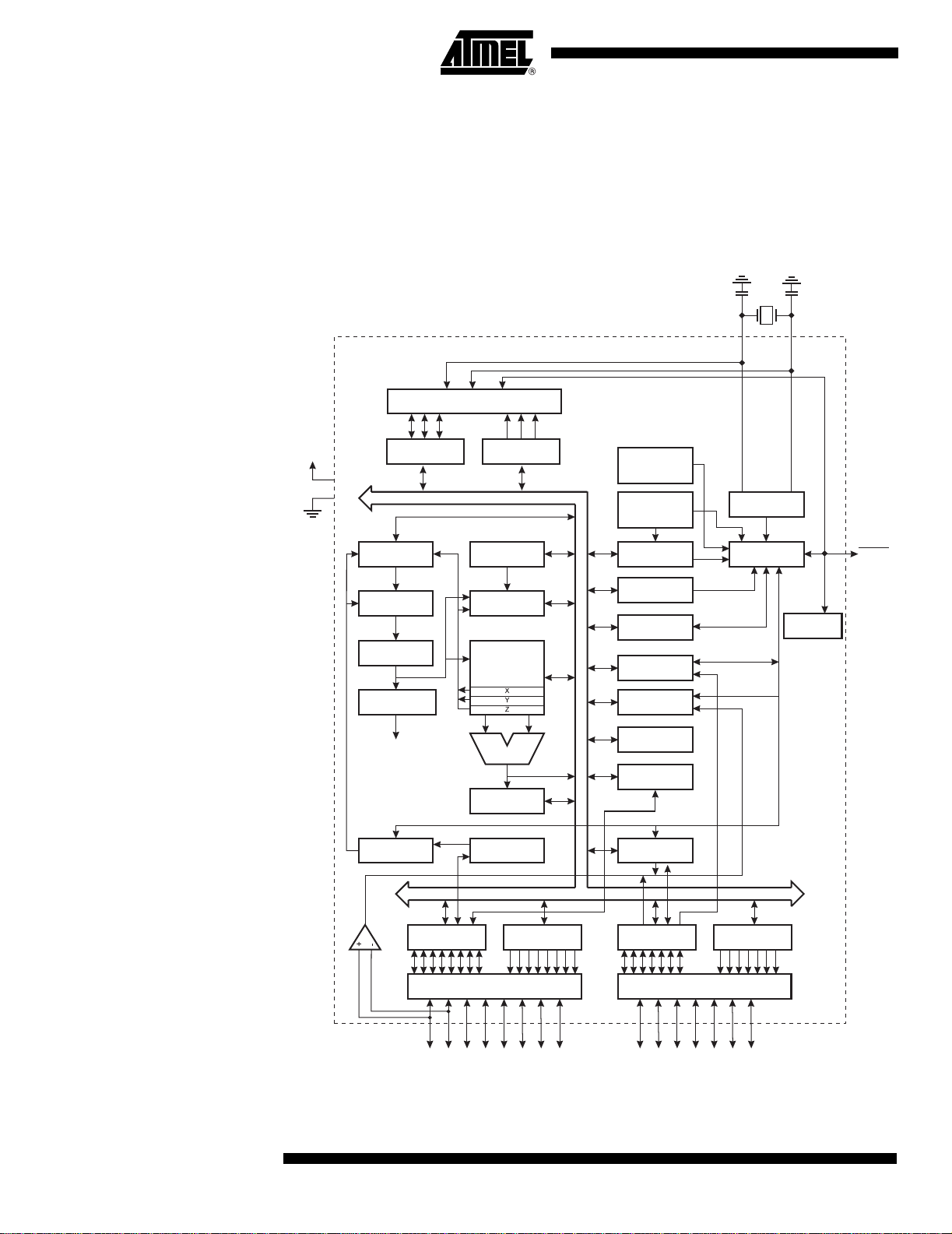
Overview The ATtiny2313 is a low-power CMOS 8-bit microcontroller based on the AVR
enhanced RISC architecture. By executing powerful instructions in a single clock cycle,
the ATtiny2313 achieves throughputs appr oaching 1 MIPS per MHz allowing the system
designer to optimize power consumption versus processing speed.
Block Diagram
Figure 2. Block Diagram
VCC
GND
DATA REGISTER
PORTA
PROGRAM
COUNTER
PROGRAM
FLASH
INSTRUCTION
REGISTER
INSTRUCTION
DECODER
CONTROL
LINES
PA0 - PA 2
PORTA DRIVERS
REG. PORTA
STACK
POINTER
SRAM
GENERAL
PURPOSE
REGISTER
ALU
STATUS
REGISTER
DATA DIR.
8-BIT DATA BUS
INTERNAL
CALIBRATED
OSCILLATOR
INTERNAL
OSCILLATOR
WATCHDOG
TIMER
MCU CONTROL
REGISTER
MCU STATUS
REGISTER
TIMER/
COUNTERS
INTERRUPT
UNIT
EEPROM
USI
XTAL1
OSCILLATOR
TIMING AND
CONTROL
XTAL2
ON-CHIP
DEBUGGER
RESET
PROGRAMMING
LOGIC
DATA REGISTER
PORTB
ANALOG
COMPARATOR
2
ATtiny2313
SPI
REG. PORTB
PORTB DRIVERS
PB0 - PB7
DATA DIR.
USART
DATA REGISTER
PORTD
PORTD DRIVERS
PD0 - PD6
DATA DIR.
REG. PORTD
2543A–AVR–08/03
Page 3

ATtiny2313
The AVR core combines a ric h instr uctio n set wit h 32 general purpose worki ng regi sters .
All the 32 regi sters are dire ctly conn ected to the Arithm etic Logic U nit (A LU), all owing
two independent regist ers t o be acces sed i n one sing le inst ructi on execut ed in one clo ck
cycle. The resulting arc hitect ur e is more code eff icient whil e achievi ng throug hput s up to
ten times faster than conventional CISC microcontrollers.
The ATtiny2313 provides the fol lowing features: 2K bytes of In-System Programm able
Flash, 128 bytes EEPROM, 128 bytes SRAM, 18 general purpose I/O lines, 32 general
purpose wo rking re giste rs, a singl e-wire Inte rface f or O n-chip Debu ggi ng, two fle xible
Timer/Counters with compare modes, internal and external interrupts, a serial programmable USART, Universal Serial Int erface wi th Star t Condition Detector , a progra mmable
Watchdog Timer with internal Oscillator, and three sof tware sele ctable p ower savin g
modes. The Idle m ode stops the CPU whil e allowing the SRAM, Ti mer/Cou nters, and
interrupt system to continue functioning. The Power-down mode saves the register contents but freezes the Oscillator, disabling all other chip functions until the next interrupt
or hardware reset. In Standby mode, the cryst al/resonator Oscillator is running while t he
rest of the devic e is sleeping . This allo ws very fast sta rt-up com bined with low-pow er
consumption.
The device is manufactured using Atmel’s high density non-volatile memory technology.
The On-chip ISP Flash allows the program memory to be reprogrammed In-System
through an SPI serial interface, or by a conventional non-volatile memory programmer.
By combining an 8-bit RISC CPU with In-System Self-Programmable Flash on a monolithic chip, the Atmel ATtiny2313 is a powerful microcontroller that provides a highly
flexible and cost effective solution to many embedded control applications.
The ATtiny2313 AVR is supported with a full suite of program and system development
tools including: C Compilers, Macro Assemblers, Program Debugger/Simulators, In-Circuit Emulators, and Evaluation kits.
2543A–AVR–08/03
3
Page 4

Pin Descriptions
VCC Digital supply voltage. GND Ground. Port A (PA2..PA0) Port A is a 3-bit bi-directional I/O port with in ternal pull-up resistors (sel ected for each
bit). The Port A output buf fers have symmetrical drive char acteristics with both high sink
and source capability. As inputs, Por t A pins that are externally p ulled low w ill source
current if the pull-up resistors are activated. The Port A pins are tri-stated when a reset
condition becomes active, even if the clock is not running.
Port A also serves the functions of various special features of the ATtiny2313 as listed
on page 54.
Port B (PB7..PB0) Port B is an 8-bit bi-directional I/O port with internal pull-up resistors (selected for each
bit). The Port B output buf fers have symmetrical drive char acteristics with both high sink
and source capability. As inputs, Por t B pins that are externally p ulled low w ill source
current if the pull-up resistors are activated. The Port B pins are tri-stated when a reset
condition becomes active, even if the clock is not running.
Port B also serves the functions of various special features of the ATtiny2313 as listed
on page 54.
Port D (PD6..PD0) Port D is a 7-bit bi-direct ional I/O port w ith intern al pull-up resistor s (selected for each
bit). The Port D output buffers have symmetri cal drive character ist ics with both high sink
and source capability. As inputs, Port D pins that are externally pulled low will source
current if the pull-up resistors are activated. The Port D pins are tri-stated when a reset
condition becomes active, even if the clock is not running.
Port D also serves the functions of various special features of the ATtiny2313 as listed
on page 57.
RESET
XTAL1 Input to the inverting Oscillator amplifier and input to the internal clock operating circuit.
XTAL2 Output from the inverting Oscillator amplifier. XTAL2 is an alternate fun cti on for PA1.
About Code Examples
Reset input. A low level on this pin for longer than the minimum pulse length will generate a reset, even if the clock is not running. The minimum pulse length is given in Table
15 on page 35. Shorter pulses are not guaranteed to generate a reset. The Reset Input
is an alternate function for PA2 and dW.
XTAL1 is an alternate function for PA0.
This documentation contai ns simpl e code examples that bri efly show how to use var ious
parts of the device. These cod e example s assume tha t the part speci fic header file is
included before compilation. Be aware that not all C compiler vendors include bit definitions in the header files and interrupt handling in C is compiler dependent. Please
confirm with the C compiler documentation for more details.
Disclaimer Typical values contained in this data sheet are based on simulations and characteriza-
tion of other AVR microcontrollers manufactured on the same process technology. Min
and Max values will be available after the device is characterized.
4
ATtiny2313
2543A–AVR–08/03
Page 5
ATtiny2313
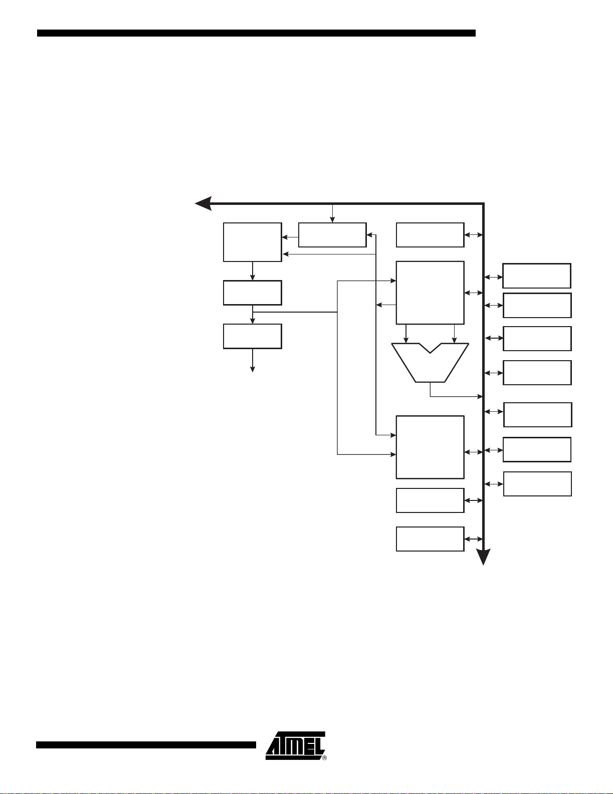
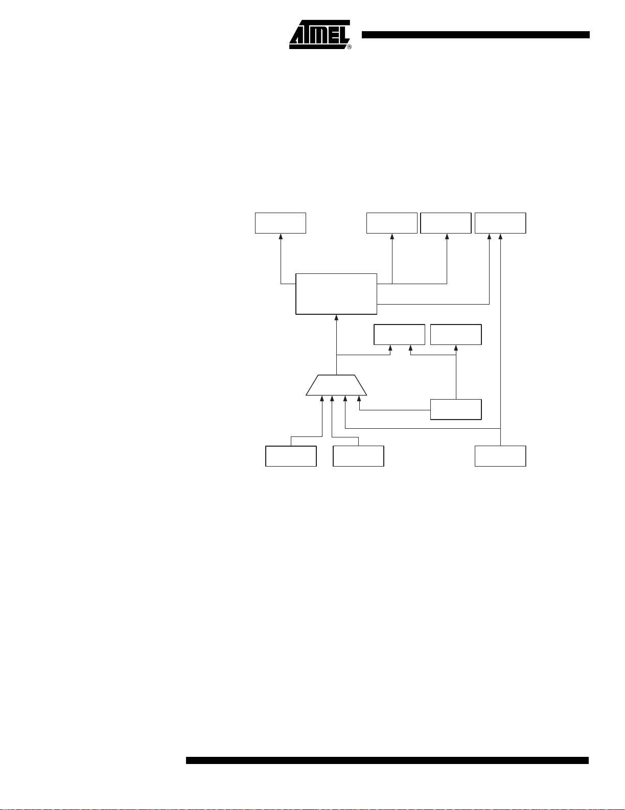
AVR CPU Core
Introduction This section discusses the AV R core architecture in general. The main function of the
CPU core is to e nsu re corre ct program exec ution. The CP U mu st there fore b e abl e to
access memories, perform cal culations, control peripher als, and handle interrupts.
Architectual Overview Figure 3. Block Diagram of the AVR Architecture
Data Bus 8-bit
Flash
Program
Memory
Instruction
Register
Instruction
Decoder
Control Lines
Program
Counter
Direct Addressing
Status
and Control
32 x 8
General
Purpose
Registrers
ALU
Indirect Addressing
Data
SRAM
EEPROM
Interrupt
Unit
SPI
Unit
Watchdog
Timer
Analog
Comparator
I/O Module1
I/O Module 2
I/O Module n
2543A–AVR–08/03
I/O Lines
In order to maximize per formance and parallelism, the AVR uses a Harvard architecture
– with separate memories and buses for program and data. Instructions in the program
memory are executed with a single level pipelining. While one instruction is being executed, the next instruction is pre-fetched from the program memory. This concept
enables instructions to be executed in every clock cycle. The program memory is InSystem Reprogrammable Flash memory.
The fast-access Regist er File contains 32 x 8-bit general purpose working registers with
a single clock cycle a ccess time. This a llows single -cycle Arithmetic Logic Unit (ALU)
operation. In a typical AL U operation, two operands are out put from the Registe r File,
5
Page 6

the operation is executed, and the result is stored back in the Register File – in one
clock cycle.
Six of the 32 registers can be used as three 16-bit indirect address register pointers for
Data Space addressing – enabling efficient address calculations. One of the these
address pointers can also be used as an addres s pointer for look up ta bles in Flash program memory. These adde d function registers are the 1 6-bit X-, Y-, and Z-register,
described later in t his section.
The ALU supports arithmetic and logic operations between registers or between a constant and a register. Single register operations can also be executed in the ALU. After
an arithmetic operation, the St atus Regist er is updat ed to reflect i nformation a bout the
result of the operation.
Program flow is provided by conditional and unconditional jump and call instructions,
able to directly address the whole address space. Most AVR instructions have a single
16-bit word format. Every program memory address contains a 16- or 32-bit instruction.
During interrupts and subroutine cal ls, the return address Program Counter (PC) is
stored on the Stack . Th e Stac k is effectiv ely al locat ed in t he general data SRAM , a nd
consequently the Stack size is only limited by the total SRAM size and the usage of the
SRAM. All user programs must initialize the SP in the Reset routine (bef ore subroutines
or interrupts are exe cuted). The S tack Pointer (SP ) is read/wri te accessible in the I/O
space. The data SRAM can easily be accessed through the five different addressing
modes supported in the AVR architecture.
The memory spaces in the AVR architecture are all linear and regular memory maps.
ALU – Arithmetic Logic Unit
A flexible inte rrupt modu le has its con trol regist ers in the I/O space with an additio nal
Global Interrupt Enabl e bit in the St atus Regis ter. All i nterr upts have a sep arat e Interrup t
Vector in the Interrupt Vector table. The interrupts have priority in accordance with their
Interrupt Vector pos ition. The lower the Interrupt Vect or address, the higher the priorit y.
The I/O memory space contains 64 addresses for CPU peripheral functions as Control
Registers, and other I/O functions. The I/O Memory can be accessed directly, or as the
Data Space locations following thos e of the Regi ster File, 0x20 - 0x5F.
The high-performance AVR ALU operates in direct connection with all the 32 general
purpose worki ng register s. Withi n a single cl ock cycle, arithmet ic operat ions betw een
general purp ose regis ters or be tween a re giste r and an imme diate ar e ex ecuted . T he
ALU operations are divided i nto three main categories – ari thmet ic, logical, and bit-functions. Some implementations of the architecture also provide a powerful multiplier
supporting both signed/unsi gned m ultiplic ation and fractio nal format. See the “Ins truction Set” section for a detailed description.
6
ATtiny2313
2543A–AVR–08/03
Page 7

ATtiny2313
Status Register The Status Register contains information about the result of the most recently executed
arithmetic instruction. This information can be used for altering program flow in order to
perform conditi onal opera tions. Note that the Stat us Registe r is update d after all AL U
operations, as specified in the Instruction Set Reference. This will in many cases
remove the need for using the dedicated compare instructions, resulting in faster and
more compact code.
The Status Register is not a utomaticall y stored wh en ent ering an i nterrupt routine and
restored when returning from an interrupt. This must be handled by software.
The AVR Status Register – SREG – is defined as:
Bit 76543210
I T H S V N Z C SREG
Read/Write R/W R/W R/W R/W R/W R/W R/W R/W
Initial Value00000000
• Bit 7 – I: Glob a l In te r ru p t En a b le
The Global Interrupt Enable bit must be set for the interrupts to be enabled. The individual interrupt enable control is then performed in separate control registers. If the Global
Interrupt Enable Register is cleared, none of the interrupts are enabled independent of
the individual interrupt enable sett ings. The I-bit is cl eared by hardwar e after an in terrup t
has occurred, and is set by the RETI instruction to enable subsequent interrupts. The Ibit can also be set and cleared by the application with the SEI and CLI instructions, as
described in the instruction set reference.
• Bit 6 – T: Bit Copy Storage
The Bit Copy instructions BLD (Bit LoaD) and BST (Bit STore) use the T-bit as sour ce or
destination for the operated bit. A bit from a register in the Reg ister File can be copied
into T by the BST instruction, and a bit i n T can be copied into a b it in a reg ister in the
Register File by the BLD instruct ion.
• Bit 5 – H: Half Car ry F la g
The Half Carry Flag H indicates a Half Carry in some arith metic opera tions. Half Carry Is
useful in BCD arithmetic. See the “Instru cti on Set Description” for detailed information.
• Bit 4 – S: Sign Bit, S = N
⊕ V
The S-bit is always an exclusive or between the negative flag N and the Two’s Complement Overflow Flag V. See the “Instruction Set Descr iption” for detailed information.
• Bit 3 – V: Two’s Complement Overflow Flag
The Two’s C omplem ent O verflow Fla g V s upports two’s compl eme nt a rithmet ics. S ee
the “Instruction Set Descr iption” for detailed information.
• Bit 2 – N: Negative Flag
The Negative Flag N indicates a negative result in an arithmetic or logic operation. See
the “Instruction Set Descr iption” for detailed information.
2543A–AVR–08/03
• Bit 1 – Z: Zero Flag
The Zero Flag Z indicates a zero result i n an arith metic or logic operation. S ee the
“Instruction Set Description” for detailed information.
7
Page 8

• Bit 0 – C: Carry Flag
The Carry Flag C indicates a carry in an arithmetic or logic operation. See the “Instruction Set Description” for detailed information.
General Purpose Register File
The Register F ile is optim ized f or the A VR E nhanc ed RIS C in struction set. I n orde r to
achieve the required performance and flexibility, the following input/output schemes are
supported by the Register File:
• One 8-bit output operand and one 8-bit result input
• Two 8-bit output operands and one 8-bit result input
• Two 8-bit output operands and one 16-bit result input
• One 16-bit output operand and one 16-bit result input
Figure 4 shows the structure of the 32 general purpose working registers in the CPU.
Figure 4. AVR CPU General Purpose Working Registers
70Addr.
R0 0x00
R1 0x01
R2 0x02
…
R13 0x0D
General R14 0x0E
Purpose R15 0x0F
Working R16 0x10
Registers R17 0x11
…
R26 0x1A X-register Low Byte
R27 0x1B X-register High Byte
R28 0x1C Y-register Low Byte
R29 0x1D Y-register High Byte
R30 0x1E Z-register Low Byte
R31 0x1F Z-register High Byte
Most of the instruction s operati ng on the Regist er File have di rec t access to al l regi sters ,
and most of them are single cycle instructions.
As shown in Figure 4, each register is also assigned a data memory address, mapping
them directly into the first 32 locations of the user Data Space. Although not being physically implemented as SRAM locations, t his memory organizati on provides great
flexibility in acces s of the regi sters, as the X-, Y- and Z -pointe r registe rs can b e s et to
index any register in the file.
8
ATtiny2313
2543A–AVR–08/03
Page 9
ATtiny2313
The X-register, Y- regi ster, and Z-register
The registers R26..R31 have some added functions to their general purpose usage.
These registers are 16-bit address pointers for indirect addressing of the data space.
The three indirect address registers X, Y, and Z are defined as described in Figure 5.
Figure 5. The X-, Y-, and Z-registers
15 XH XL 0
X-register 7 0 7 0
R27 (0x1B) R26 (0x1A)
15 YH YL 0
Y-register 7 0 7 0
R29 (0x1D) R28 (0x1C)
15 ZH ZL 0
Z-register 7 0 7 0
R31 (0x1F) R30 (0x1E)
In the different addressi ng mode s these ad dress registe rs have f unctions as f ixed di splacement, autom atic increment, and aut omatic decreme nt (see the instruction set
reference for details).
Stack Pointer The Stack is mainly used for storing temp orary data, for storing l ocal variables and for
storing return addresses after interrupts and subroutine calls. The Stack Pointer Register always points to the top of the Stack. Note that the Stack is implemented as growing
from higher memory locati ons to lower mem ory locations. This implies that a Stack
PUSH command decreases the Stack Pointer.
The Stack Pointer points to the data SRAM Stack area where the Subroutine and Interrupt Stacks are located. This Stack space in the data SRAM must be defined by the
program before any subroutine calls are executed or interrupts are enabled. The Stack
Pointer must be set to point a bove 0x60. The Stack Poi nter is decremented by one
when data is pushed ont o the Stack with the PUSH instruction, and it is decremented by
two when the return address is pushed onto the Stack with subroutine call or interrupt.
The Stack Pointer is incremented by one when dat a is popped f rom the Stack with the
POP instruction, and it is incremented by two when data is popped from the Stack with
return from subroutine RET or return from interrupt RETI.
The AVR Stack Pointer is implemented as two 8-bit registers in the I/O space. The number of bits actually used i s implementation dependent. Note that the data space in some
implementations of the AVR architecture is so small that only SPL is needed. In this
case, the SPH Register will not be present.
Bit 1514131211109 8
––––––––SPH
SP7 SP6 SP5 SP4 SP3 SP2 SP1 SP0 SPL
76543210
Read/WriteRRRRRRRR
R/W R/W R/W R/W R/W R/W R/W R/W
Initial Value00000000
00000000
2543A–AVR–08/03
9
Page 10
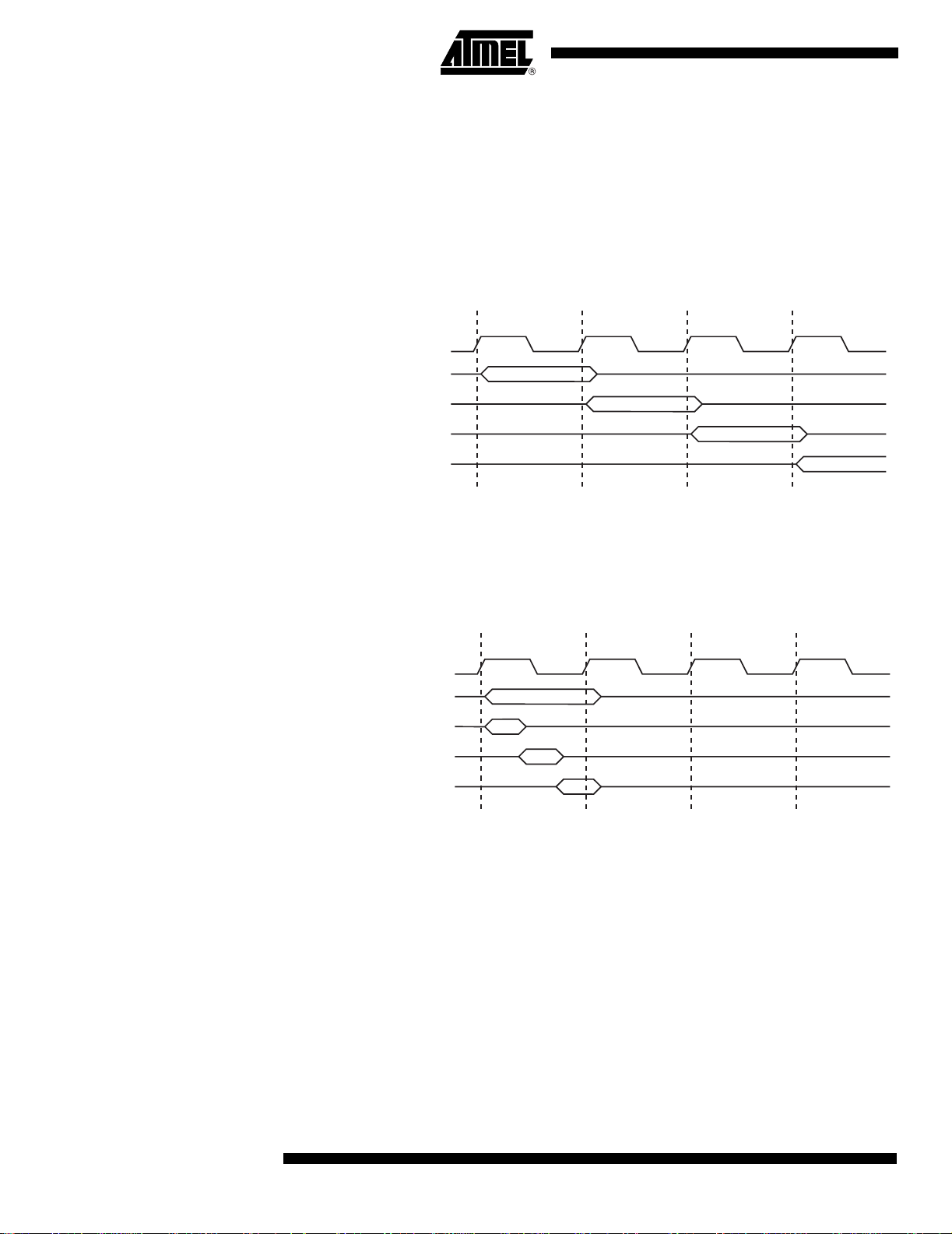
Instruction Execution Timing
This section describes the gener al access timing conc epts for i nstruct ion execut ion. The
AVR CPU is driven by the CPU clock clk
, directly generated from the selected clock
CPU
source for the chip. No internal clock division is used.
Figure 6 shows the parallel instructi on fetches and instruc tion exec utions enab led by the
Harvard architecture and the fast-access Register Fil e concept. This is the basic pipelining concept t o obtain up t o 1 M IPS p er MH z with t he co rrespondin g u nique res ults for
functions per cost, functions per clocks, and functions per power-unit.
Figure 6. The Parallel Instruc ti on Fetches and Instruction Executions
T1 T2 T3 T4
clk
CPU
1st Instruction Fetch
1st Instruction Execute
2nd Instruction Fetch
2nd Instruction Execute
3rd Instruction Fetch
3rd Instruction Execute
4th Instruction Fetch
Figure 7 shows the internal timing concept for the Register File. In a single clock cycle
an ALU operation using two register operands is executed, and the result is stored back
to the destination regis ter.
Reset and Interrupt Handling
Figure 7. Single Cycle ALU Operation
T1 T2 T3 T4
clk
CPU
Total Execution Time
Register Operands Fetch
ALU Operation Execute
Result Write Back
The AVR provides several different interrupt sources. These interrupts and the separate
Reset Vector each have a separate program vector in t he program memo ry space. Al l
interrupts are assigned indi vidual en able bits w hich must b e wr itten logic one together
with the Global Interrupt Enable bit in t he Status Register in order to enable the interrupt .
The lowest addresses in the p rogram memory spa ce are by def ault def ined as t he Rese t
and Interrupt Vectors. The complete list of vectors is shown in “Interrupts” on page 45.
The list also determines the priori ty levels of the different interrupts. The lower the
address the higher is the priority level. RESET has the highest priority, and next is INT0
– the External Inte rrupt Request 0. Ref er to “ Inter rupts” on page 45 for more i nformat ion .
When an interrupt occurs, the Global In terrupt Enab le I-bit is cleared and al l interrupts
are disabled. The user softw are ca n wri te logi c on e to the I-bit t o en able n este d int errupts. All enabled interrupts can then i nterrupt the current interrupt routine. The I-bit is
automatically set when a Return from Interrupt instruction – RETI – is executed.
10
ATtiny2313
2543A–AVR–08/03
Page 11

ATtiny2313
There are basicall y two types of inter rupts. The first type is triggered by an event that
sets the interrupt flag. For these interrupts, the P rogram Counter i s vectored to the
actual Interrupt Vector in order to execute the interrupt handling routine, and hardware
clears the corresponding interrupt flag. Interrupt flags can also be cleared by writing a
logic one to the flag bi t posi tion( s) to be c leared. If an i nterr upt condi tion oc curs whil e the
corresponding interru pt ena ble bit is cleared , the inte rrupt flag w ill be set an d rem embered until the interrupt is enabled, or the flag is cleared by software. Similarly, if one or
more interrupt conditions occur while the Global Interrupt Enable bit is cleared, the corresponding interrupt flag(s) will be set and remembered until th e Global Interrupt Enable
bit is set, and will then be executed by order of pri ority.
The second type of interrupts will trigger as long as the interrupt condition is present.
These interrupts do not necessarily have interrupt flags. If the interrupt condition disappears before the interrupt is enabled, the interrupt will not be tri ggered.
When the AVR exits from an interrupt, it will always return to the main pr ogram and execute one more instruction before any pending interrupt is served.
Note that the Status Register is not automatically stored when entering an interrupt routine, nor restored when returning from an interrupt routine. This must be handled by
software.
When using the CLI instruction to disable interrupts, the interrupts will be immediately
disabled. No interrupt wil l be executed after the CLI instruction, even if it occ urs simultaneously with the CLI instruction. The following example shows how this can be used to
avoid interrupts during the timed EEPROM write sequence..
Assembly Code Example
in r16, SREG ; store SREG value
cli ; disable interrupts during timed sequence
sbi EECR, EEMWE ; start EEPROM write
sbi EECR, EEWE
out SREG, r16 ; restore SREG value (I-bit)
C Code Example
char cSREG;
cSREG = SREG; /* store SREG value */
/* disable interrupts during timed sequence */
_CLI();
EECR |= (1<<EEMWE); /* start EEPROM write */
EECR |= (1<<EEWE);
SREG = cSREG; /* restore SREG value (I-bit) */
2543A–AVR–08/03
11
Page 12

When using the SEI instruction to enable interrupts, the instruction following SEI will be
executed before any pending inter rupt s, as shown in this example.
Assembly Code Example
sei ; set Global Interrupt Enable
sleep ; enter sleep, waiting for interrupt
; note: will enter sleep before any pending
; interrupt(s)
C Code Example
_SEI(); /* set Global Interrupt Enable */
_SLEEP(); /* enter sleep, waiting for interrupt */
/* note: will enter sleep before any pending interrupt(s) */
Interrupt Response Time The interrupt execution response for all the enabled AVR interrupts is four clock cycles
minimum. After four clock cycles the program vector address for the actual interrupt
handling routine is executed. During this four clock cycle period, the Program Counter is
pushed onto the Stack. The vect or i s normall y a jum p to t he int errupt routin e, and thi s
jump takes three clock cycles. If an interrupt occurs during execution of a multi-cycle
instruction, this instruction is completed before the interrupt is served. If an interrupt
occurs when the MCU is in sleep mode, the interrupt execution response time is
increased by four clock cycles. This increase comes in additio n to the st art-up time from
the selected sleep mode.
A return from an interrupt handling routine takes four clock cycles. During these four
clock cycles, t he Program Counter (two bytes) is popped back from the St ack, the Stack
Pointer is incremented by two, and the I-bit in SREG is set.
12
ATtiny2313
2543A–AVR–08/03
Page 13

ATtiny2313
F
AVR ATtiny2313 Memories
In-System Reprogrammable Flash Program Memory
This section describes the different memories in the ATtiny2313. The AVR architecture
has two main memory spaces, the Data Memory and the Program Memory space. In
addition, the ATtiny2313 features an EEPROM Memory for data storage. All three memory spaces are linear and regular.
The ATtiny2313 contains 2K bytes On-chip In-System Reprogrammable Flash memory
for program storage. Since all AVR instr uctions are 16 or 32 bi ts wide, the Flash is organized as 1K x 16.
The Flash me mory has an endurance of at least 10 ,000 write/erase cycles. The
ATtiny2313 Program Counter (PC) is 10 bits wide, thus addressing the 1K program
memory locations. “Memory Programming” on page 160 contains a detailed description
on Flash data serial downloading using the SPI pins.
Constant tables can be allocated within the entire program memory address space (see
the LPM – Load Program Memory instruction description) .
Timing diagrams for instruction fetch and execution are presented in “Instruction Execution Timing” on page 10.
Figure 8. Program Memory Map
Program Memory
0x0000
0x03F
SRAM Data Memory Figure 9 shows how the ATtiny2313 SRAM Memory is organized.
The lower 224 data memory locations address bot h the Regi ster File, the I/O mem ory,
Extended I/O memo ry, and the internal data SR AM. The first 32 locations address the
2543A–AVR–08/03
13
Page 14

Register File, the next 64 location the standard I/O memory, and the next 128 locations
address the internal data SRAM.
The five dif ferent addressing modes for the data memory cover: Direct, Indire ct with Displacement, Indirect, Indirect with Pre-decrement, and Indirect with Post-increment. In
the Register File, registers R26 to R31 feature the indirect addressing pointer registers.
The direct addressing rea ches the entire data space.
The Indirect with Displacement mode reaches 63 address locations from the base
address given by the Y- or Z-register.
When using register indirect addressing modes with automatic pre-decrement and post-
increment, the address regis ter s X, Y, and Z are decremented or incremented.
The 32 general purpose working registers, 64 I/O Registers, and the 128 bytes of inter-
nal data SRAM in the ATtiny2313 are all accessible through all these addressing
modes. The Register File is described in “General Purpose Register File” on page 8.
Figure 9. Data Memory Map
Data Memory
32 Registers
64 I/O Registers
Internal SRAM
(128 x 8)
0x0000 - 0x001F
0x0020 - 0x005F
0x0060
0x00DF
14
ATtiny2313
2543A–AVR–08/03
Page 15
ATtiny2313
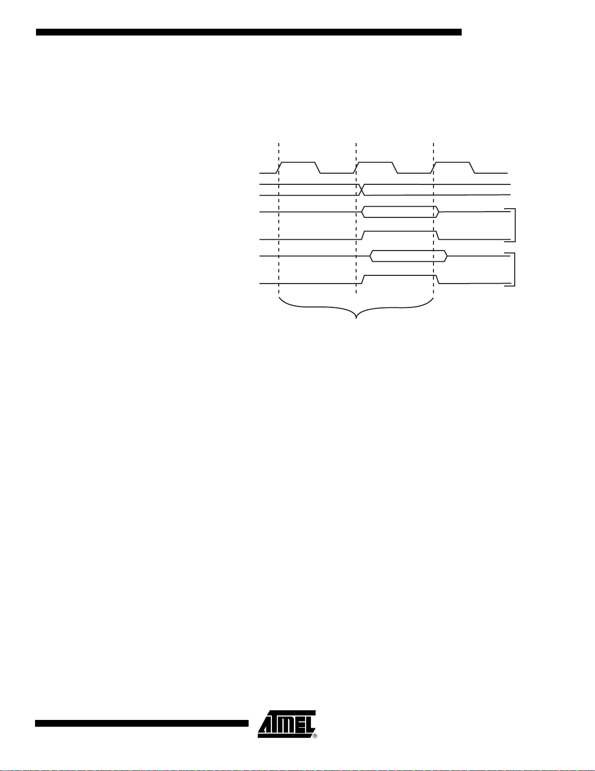
Data Memory Access Times This section describes the general access timing concepts for internal memory access.
The internal data SRAM access is performed in two clk
10.
Figure 10. On-chip Data SRAM Access Cycles
T1 T2 T3
clk
CPU
Address
Compute Address
Address valid
Data
cycles as described in Figure
CPU
WR
Write
Data
RD
Memory Access Instruction
Next Instruction
Read
EEPROM Data Memory The ATtiny2313 contains 128 bytes of data EEPROM memory. It is organized as a sep-
arate data space, in which single bytes can be read and written. The EEPROM has an
enduranc e of at lea st 100, 000 write /erase cycle s. The acc ess be tween th e EEPR OM
and the CPU is described in the following, specifying the EEPROM Address Registers,
the EEPROM Data Register, and the EEPROM Control Register. For a detailed description of Serial data downloading to the EEPROM, see page 173.
EEPROM Read/Write Access The EEPROM Access Registers are accessible in the I/O space.
The write access time for the EEPROM is given in Table 1. A self-timing function, however, lets the us er softw are detec t wh en the n ext b yte can be written. If the u ser code
contains instructions that write the EEPROM, some precautions must be taken. In
heavily filtered power suppl ies, V
causes the device for some period of time to run at a voltage lower than specified as
minimum for the clock frequency used. See “Preventing EEPROM Corruption” on page
20. for details on how to avoid problems in these situations.
is likely to rise or fall slowly on power-up/down. This
CC
2543A–AVR–08/03
In order to prevent unintenti onal EEPROM writes, a specific wr ite pro cedure must be f ollowed. Refer to the description of the EEPROM Control Register for details on this.
When the EEPROM is read, the CPU i s halted for four clock cycles before the next
instruction is execut ed. Wh en the E EPRO M is w ritten, the CPU is h alted fo r two cl ock
cycles before the next instr u ction is executed.
15
Page 16

The EEPROM Address Register
Bit 76543210
– EEAR6 EEAR5 EEAR4 EEAR3 EEAR2 EEAR1 EEAR0 EEAR
Read/Write R R/W R/W R/W R/W R/W R/W R/W
Initial Value 0 X X X X X X X
• Bit 7 – Res: Reserved Bit
This bit is reserved in the ATtiny2313 and will always read as zero.
• Bits 6..0 – EEAR6..0: EEPROM Address
The EEPROM Address Register – EEAR specify the EEPROM address in the 128 bytes
EEPROM space. The EEPROM data bytes are addressed linearly between 0 and 127.
The initial value of EEAR is undefined. A proper value must be written before the
EEPROM may be accessed.
The EEPROM Data Register – EEDR
The EEPROM Control Register – EECR
Bit 76543210
MSB LSB EEDR
Read/Write R/W R/W R/W R/W R/W R/W R/W R/W
Initial Value00000000
• Bits 7..0 – EEDR7..0: EEPROM Data
For the EEPROM write operation, the EEDR Register contains the data to be written to
the EEPROM in the address given by the EEAR Register. For the EEPROM read operation, the EEDR contains the data read out from the EEPROM at the address given by
EEAR.
Bit 76543210
– – EEPM1 EEPM0 EERIE EEMPE EEPE EERE EECR
Read/Write R R R/W R/W R/W R/W R/W R/W
Initial Value 0 0 X X 0 0 X 0
• Bits 7..6 – Res: Reserved Bits
These bits are reserved bits in t he ATtiny2313 and will always read as zero.
• Bits 5, 4 – EEPM1 and EEPM0: EEPROM Programming Mode Bits
The EEPROM Program ming mode bits setting def ines which prog ramming action that
will be triggered when writing EEPE. It is possible to program data in one atomic operation (erase the old value and program the new value) or to split the Erase and Write
operations in two differen t operations. T he Program ming times for the different m odes
are shown in Table 1. While EEPE is set, any write to EEPMn will be ignored. During
reset, the EEPMn bits will be reset to 0b00 unless the EEPROM is busy programming.
16
ATtiny2313
Table 1. EEPROM Mode Bits
Programming
EEPM1 EEPM0
0 0 3.4 ms Erase and Write in one operation (Atomic Operation)
Time Operation
2543A–AVR–08/03
Page 17

ATtiny2313
Table 1. EEPROM Mode Bits
Programming
EEPM1 EEPM0
0 1 1.8 ms Erase Only
1 0 1.8 ms Write Only
1 1 – Reserved for future use
• Bit 3 – EERIE: EEPROM Ready Interrupt Enable
Writing EERIE to one enables the EEPROM Ready Interrupt if the I-bit in SREG is set.
Writing EERIE to zero disables the interrupt. The EEPROM Ready Interrupt generates a
constant interrupt when Non-volatile memory is ready for programming.
• Bit 2 – EEMPE: EEPROM Master Program Enable
The EEMPE bit determines whether writing EEPE to one will have effect or not.
When EEMPE is set, setting EEPE within four clock cycles wi ll program the EEPROM at
the selected address. If EEMPE is zero, setting EEPE will have no effect. When EEMPE
has been written to one by software, hardware clears the bit to zero after four clock
cycles.
Time Operation
• Bit 1 – EEPE: EEPROM Program Enable
The EEPR OM P rog ram Enabl e S ignal EE PE is th e pr ogram ming enab le sign al t o the
EEPROM. When EEPE is written, the EEPROM will be programmed according to the
EEPMn bits setting. The EEMPE bit must be written to one before a logical one is written to EEPE, otherwis e no EEPROM write takes pl ace. When the write a ccess time has
elapsed, the EEP E bit is cleared by hardwa re. When EEPE has been set , the CPU is
halted for two cycles before the next instruction is executed.
• Bit 0 – EERE: EEPROM Read Enable
The EEPROM Read Enable Signal – EERE – is the read strobe to the EEPROM. When
the correct address is set up in the EEAR Register, the EERE bit must be written to one
to trigger the EEPROM read. The EEPROM read access takes one instruction, and the
requested data is available immediately. When the EEPROM is read, the CPU is halted
for four cycles before the next instruction is executed. The user should poll the EEPE bit
before starting th e read operati on. If a write oper at ion is in progress, it i s ne ither possi ble
to read the EEPROM, nor to change the EEAR Register.
Atomic Byte Programming Using Atomic B yte Prog ramming is the si mplest mo de. When writin g a byte to the
EEPROM, the user must write the address into the EEAR Register and data into EEDR
Register. If the EEPMn bits are zero, writing EEPE (wi thin four cycles after EEMPE is
written) will trigger the erase/write operation. Both the erase and write cycle are done in
one operation and the total programming time is given in Table 1. The EEPE bit remains
set until the erase and write operations are completed. While the device is busy with
programming, it is not possible to do any other EEPROM operations.
Split Byte Programming It is possible to split the erase and wri te cycle in two d ifferent operations. Th is may be
useful if the system requires short access time for some limited period of time (typically
if the power supply voltage fal ls). In order to t ake advantage of this method, it is req uired
that the locations to be w ritten have be en eras ed before the write op eration. But si nce
the erase and write op erations are split, it is possi ble to do t he erase o perations w hen
the system allows doing time-cons uming operations (typically after Power-up).
17
2543A–AVR–08/03
Page 18

Erase To erase a byte, the address must be written to EEAR. If the EEPMn bits are 0b01, writ-
ing the EEPE (within four cycles after EEMPE is written) will trigger the erase operation
only (programming time is given in Table 1). The EEPE bit remai ns set until the erase
operation completes. While the device is busy programming, it is not possible to do any
other EEPROM operations.
Write To write a location, the user must write the address into EEAR and the data into EEDR.
If the EEPMn bits are 0b10, wri ti ng the EEPE (within four cycles after EEMPE is written)
will trigger the write operation only (programming time is give n in Table 1). The EE PE
bit remains set until the write o peration co mpletes . If the l ocation to be writ ten has not
been erased before write, the data that is stored must be considered as lost. While the
device is busy with programming, it is not possible to do any other EEPROM operations.
The calibrated Oscillator is used to time the EEPROM accesses. Make sure the Oscillator frequency is with in the requirements desc ribed in “Oscillator C alibration R egister –
OSCCAL” on page 26.
18
ATtiny2313
2543A–AVR–08/03
Page 19

ATtiny2313
The following code examples show one assembly and on e C function for writing to the
EEPROM. The examples assume t hat interrupts are controlled (e.g. by disabling interrupts globally) so that no interrupts will occur during execution of these functions.
Assembly Code Example
EEPROM_write:
; Wait for completion of previous write
sbic EECR,EEWE
rjmp EEPROM_write
; Set up address (r17) in address register
out EEAR, r17
; Write data (r16) to data register
out EEDR,r16
; Write logical one to EEMWE
sbi EECR,EEMW E
; Start eeprom wri te by setting EEWE
sbi EECR,EEWE
ret
C Code Example
void EEPROM_write(uns igned int uiAddress, unsigned char ucData)
{
/* Wait for completion of previous write */
while(EECR & (1<<EEWE))
;
/* Set up address and data registers */
EEAR = uiAddress;
EEDR = ucData;
/* Write logical one to EEMWE */
EECR |= (1<<EEMWE);
/* Start eeprom write by setting EEWE */
EECR |= (1<<EEWE);
}
2543A–AVR–08/03
19
Page 20

The next code examples show assembly and C functions for reading the EEPROM. The
examples assume that interru pts are controlled so that no interrupts will occur during
execution of these functions.
Assembly Code Example
EEPROM_read:
; Wait for completion of previous write
sbic EECR,EEWE
rjmp EEPROM_read
; Set up address (r17) in address register
out EEAR, r17
; Start eeprom read by writing EERE
sbi EECR,EERE
; Read data from data register
in r16,EEDR
ret
C Code Example
unsigned char EEPROM_read(unsigned int uiAddress)
{
/* Wait for completion of previous write */
while(EECR & (1<<EEWE))
;
/* Set up address reg ister */
EEAR = uiAddress;
/* Start eeprom read by writing EERE */
EECR |= (1<<EERE);
/* Return data from data register */
return EEDR;
}
Preventing EEPROM Corruption
20
ATtiny2313
During periods of low V
the EEPROM data can be corrupted because the supply volt-
CC,
age is too low for the CPU and the EEPROM to operate properly. These issues are the
same as for board level systems using EEPROM, and the same design solutions should
be applied.
An EEPROM data corruption can be caused by two situations wh en the voltage is too
low. First, a regular write sequence to t he EEPROM requires a minimum volt age to
operate correctly. Second ly, the CPU itself can execute ins tructions incorrectly , if the
supply voltage is too low.
EEPROM da ta corruption can easily be avoided by fol lowing this design
recommendation:
Keep the AVR RESET ac tive (low) during periods of insuf ficient power supp ly voltage.
This can be do ne by enab ling the i nternal B rown- out Detect or (BOD). If the de tection
level of the internal BOD does not match the needed detection level, an external low
reset Protecti on circ uit ca n be used. If a re set occurs w hile a write ope ration i s in
V
CC
progress, the write oper ation will be compl et ed provide d that the power supply voltage i s
sufficient.
2543A–AVR–08/03
Page 21

ATtiny2313
I/O Memory The I/O space definition of the ATtiny2313 is shown in “Register Summary” on page
198.
All ATtiny2313 I/Os and peripherals are place d in the I/O space. All I/O loc ations may be
accessed by the LD/LDS/LDD and ST/STS/STD instructions, transferring data between
the 32 general purpose working registers and the I/O space. I/O Registers within the
address range 0x00 - 0x1F are directly bit-accessible using the SBI and CBI instructions. In these registers, the value of single bits can be checked by using the SBIS and
SBIC instructions. Refer to the instruction set section for more details. When using the
I/O specific c ommand s IN and OUT, t he I/O ad dresses 0x 00 - 0 x3F mus t be used.
When addressing I/O Registers as data space using LD and ST instructions, 0x20 must
be added to these addresses.
For compatibility wit h future devices, reserved bits should be writ ten to zero if accessed.
Reserved I/O memory addresses should never be written.
Some of the status flags a re cleared by writing a l ogical one to them. Note that, u nlike
most other AVRs, the CBI and SBI instructions wi ll only operate on the specified bit, and
can therefore be used on registers containing such status flags. The CBI and SBI
instructions work with registers 0x00 to 0x1F only.
The I/O and peripherals control registers are explained in later sections.
General Purpose I/O Registers The ATtiny2313 contains three General Purpose I/O Registers. These registers can be
used for storing any information, and they are particularly useful for storing global variables and status flags. General Purpose I/O Registers within the address range 0x00 0x1F are directly bit-accessible using the SBI, CBI, SBIS, and SBIC instructions.
General Purpose I/O Register 2 – GPIOR2
Bit 76543210
MSB LSB GPIOR2
Read/Write R/W R/W R/W R/W R/W R/W R/W R/W
Initial Value00000000
General Purpose I/O Register 1 – GPIOR1
Bit 76543210
MSB LSB GPIOR1
Read/Write R/W R/W R/W R/W R/W R/W R/W R/W
Initial Value00000000
General Purpose I/O Register 0 – GPIOR0
Bit 76543210
MSB LSB GPIOR0
Read/Write R/W R/W R/W R/W R/W R/W R/W R/W
Initial Value00000000
2543A–AVR–08/03
21
Page 22
System Clock and Clock Options
Clock Systems and their Distribution
Figure 11 presen ts the princip al clo ck system s in the AV R and the ir distributi on. All of
the clocks need not be active at a given time. In order to redu ce power consump tion, the
clocks to modules not being used can be halted by using different sleep modes, as
described in “Power Management and Sleep Modes” on page 30. The clock systems
are detailed below.
Figure 11. Clock Distribution
General I/O
Modules
clk
CPU Core RAM
I/O
AVR Clock
Control Unit
Source clock
Clock
Multiplexer
clk
CPU
clk
FLASH
Reset Logic
Watchdog Timer
Watchdog clock
Watchdog
Oscillator
Flash and
EEPROM
CPU Clock – clk
I/O Clock – clk
I/O
Flash Clock – clk
CPU
FLASH
External Clock
Crystal
Oscillator
Calibrated RC
Oscillator
The CPU clock is routed to parts of the system concerned with operation of the AVR
core. Examples of such module s are the General Purpose Reg ister File, the Stat us Register and the data memory holding the Stack Pointer. Halting the CPU clock inhibits the
core from performing general operations and calculations.
The I/O clock is used by the majority of the I/O modules, like Timer/Counters, and
USART. The I/O clock is also used by the External Interrupt module, but note that some
external inter rupts are d etected by as ynchrono us logic, al lowing suc h interrup ts to be
detected even if the I/O clock i s halted . Also note that start conditi on detect ion in the USI
module is carried out asynchronously when clk
is halted, enabling USI start condition
I/O
detection in all sleep modes.
The Flash clock controls operation of the Flash interface. The Flash clock is usually
active simultaneously with th e CPU clock.
22
ATtiny2313
2543A–AVR–08/03
Page 23

ATtiny2313
Clock Sources The device has the following clock source options, selectable by Flash Fuse bits as
shown below. The clock from the selected source is input to the A VR cl ock gene rator,
and routed to the appropriate module s.
Table 2. Device Clocking Select
Device Clocking Option CKSEL3..0
External Clock 0000 - 0001
Calibrated Internal RC Oscillator 4MHz 0010 - 0011
Calibrated internal RC Oscillator 8MHz 0100 - 0101
Watchdog Oscillator 128kHz 0110 - 0111
External Crystal/Ceramic Resonator 1000 - 1111
Note: 1. For all fuses “1” means unprogrammed while “0” means programmed.
(1)
The various choices for each clocki ng optio n is given i n the followi ng secti ons. When the
CPU wakes up from Power-down, the sel ected clock source is us ed to time the start-up,
ensuring stable Oscillator operation before instruction execution starts. When the CPU
starts from reset, there is an additional delay allowing the power to reach a stable level
before commenci ng n ormal op eration . Th e Wa tchdog Os cillator i s used for timing this
real-time part of the start-up time. The number of WDT Oscillator cycles used for each
time-out is shown in Table 3. The freque ncy of the Watchdog Oscillator is voltage
dependent as shown in “ATt iny2313 Ty pic al Charac teris tics – Preli minary Dat a” on page
181.
Table 3. Number of Watchdog Oscillator Cycles
Typ Time-out (VCC = 5.0V) Typ Time-out (VCC = 3.0V) Number of Cycles
4.1 ms 4.3 ms 4K (4,096)
65 ms 69 ms 64K (65,536)
Default Clock Source The device is shipped with CKSEL = “0010”, SUT = “10”, and CKDIV8 programmed.
The default clock source setting is t he Internal R C Oscillator wit h longest start-up t ime
and an initial system clock prescaling of 8. This defaul t settin g ensur es that all user s can
make their desired clock source setting using an In-System or Parallel programmer.
2543A–AVR–08/03
23
Page 24
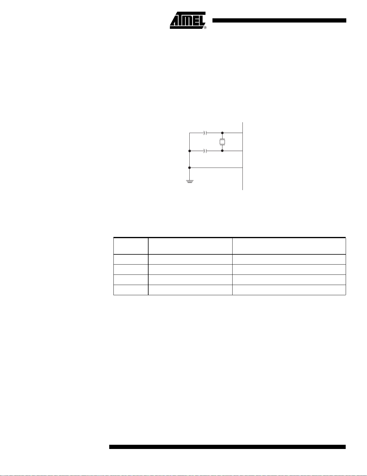
Crystal Oscillator XTAL1 and XTAL2 are input and o utput , respectively, of an inverting amplifier which can
be configured for use as an On-chip Osc illator, as shown i n F igure 12. Either a quartz
crystal or a ceramic resonator may be used.
C1 and C2 should always be equal for both crystals and resonators. The optimal value
of the capacitors depends on the crystal or resonator in use, the amount of stray capacitance, and the electromagnetic noise of the environment. Some initial guidelines for
choosing capacitors for use with crystals are given in Table 4. For ceramic resonators,
the capacitor values given by the manufacturer should be used.
Figure 12. Crystal Oscillator Connections
C2
C1
XTAL2
XTAL1
GND
The Oscillator can operate in three different modes, each optimized for a specific frequency range. The operating mode is selected by the fuses CKSEL3..1 as shown in
Table 4.
Table 4. Crystal Oscillator Operating Modes
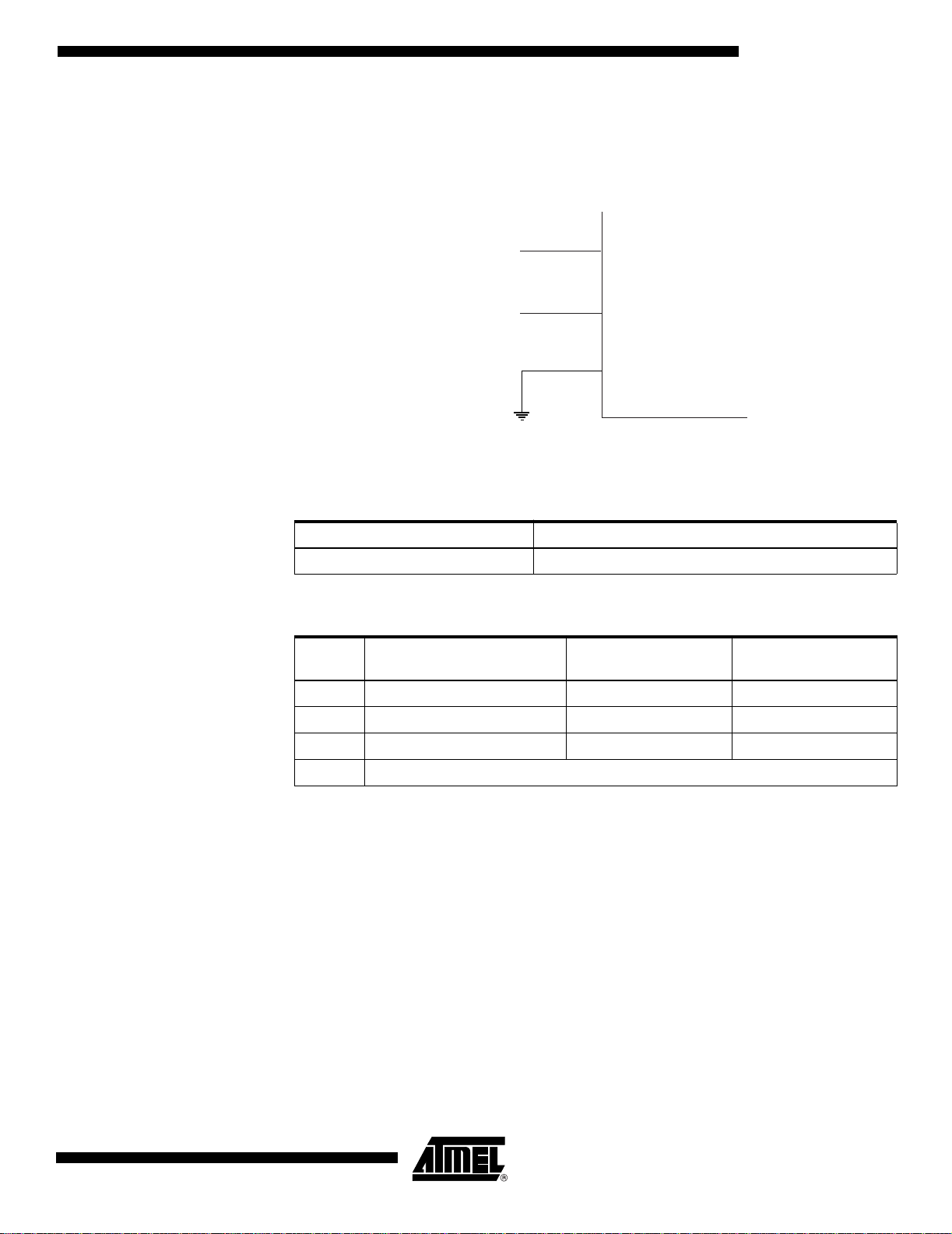
CKSEL3..1 Frequency Range
(2)
100
101 0.9 - 3.0 12 - 22
110 3.0 - 8.0 12 - 22
111 8.0 - 12 - 22
Notes: 1. The frequency ranges are preliminary values. Actual values are TBD.
2. This option should not be used with crystals, only with ceramic resonators.
0.4 - 0.9 –
(1)
(MHz)
Recommended Range for Capacitors C1
and C2 for Use with Crystals (pF)
24
The CKSEL0 Fuse together with the SUT1..0 Fuses select the start-up times as shown
in Table 5.
ATtiny2313
2543A–AVR–08/03
Page 25

Table 5. Start-up Times for the Crystal Oscillator Clock Selection
ATtiny2313
Start-up Time from
Power-down and
CKSEL0 SUT1..0
0 00 258 CK
0 01 258 CK
010 1K CK
011 1K CK
100 1K CK
1
1
1
Notes: 1. These options should only be used when not operating close to the maximum fre-
01 16K CK 14CK Crystal Oscillator, BOD
10 16K CK 14CK + 4.1 ms Crystal Oscillator, fast
11 16K CK 14CK + 65 ms Crystal Oscillator,
quency of the device, and only if frequency stability at start-up is not important for the
application. These options are not suitable for crystals.
2. These options are intended for use with ceramic resonators and will ensure frequency stability at start-up. They can also be used with crystals when not operating
close to the maximum frequency of the device, and if frequency stability at start-up is
not important for the application.
Power-save
(1)
(1)
(2)
(2)
(2)
Additional Delay
from Reset
(VCC = 5.0V) Recommended Usage
14CK + 4.1 ms Ceramic resonator, fast
rising power
14CK + 65 ms Ceramic resonator,
slowly rising power
14CK Ceramic resonator,
BOD enabled
14CK + 4.1 ms Ceramic resonator, fast
rising power
14CK + 65 ms Ceramic resonator,
slowly rising power
enabled
rising power
slowly rising power
Calibrated Internal RC Oscillator
The calibrated internal R C Oscillator provides a f ixed 8.0 MH z clock. T he frequ ency is
nominal value at 3V and 25°C. I f 8 MHz frequency exc eeds the specif ication of the
device (depends on V
), the CKDIV8 Fuse must be programmed in order to divide the
CC
internal frequency by 8 during start-up. The device is shipped with the CKDIV8 Fuse
programmed. This clock may b e selected a s the system clock by p rogramming the
CKSEL Fuses as sho wn in T able 6. If selected, it will o perate with no external com ponents. During reset, hardware loads the calibration byte into the OSCCAL Register and
thereby automaticall y calibrates the RC Oscillat or. At 3V and 25°C, this cal ibr ation gives
a frequency within ± 1% of the nom inal fr equency. When th is Osc illator is u sed as t he
chip clock, the Watchdog Oscillator will still be used for the Watchdog Timer and for the
Reset Time-out. For more information on the pre-programmed calibration value, see the
section “Calibration Byte” on page 162.
Table 6. Internal Calibrated RC Oscillator Operati ng Mo des
CKSEL3..0 Nominal Frequency
0010 - 0011 4.0 MHz
0100 - 0101 8.0 MHz
Note: 1. The device is shipped with this option selected.
(1)
2543A–AVR–08/03
25
Page 26
When this Oscilla tor is sele cted, sta rt-up times are determ ined by the SUT Fuse s as
shown in Table 7.
Table 7. Start-up times for the internal calibrated RC Oscillator clock selection
Oscillator Calibrat ion Register – OSCCAL
Start-up Time from Power-
SUT1..0
00 6 CK 14CK BOD enabled
01 6 CK 14CK + 4.1 ms Fast rising power
(1)
10
11 Reserved
Note: 1. The device is shipped with this option selected.
Bit 76543210
Read/Write R R/W R/W R/W R/W R/W R/W R/W
Initial Value Device Specific C a libra tion Value
down and Power-save
6 CK 14CK + 65 ms Slowly rising power
– CAL6 CAL5 CAL4 CAL3 CAL 2 CAL1 CAL0 OSCCAL
Additional Del ay from
Reset (VCC = 5.0V) Recommended Usage
• Bits 6..0 – CAL6..0: Oscillator Calibration Value
Writing the calibration byte to this address will trim the internal Oscillator to remove process variations from the Oscillator frequency. This is done automatically during Chip
Reset. When OSCCAL is zero, the lowest avai lable frequency is chosen. Writing nonzero values to this register will increase the frequency of the internal Oscillator. Writing
0x7F to the register gives the hi ghest availab le frequency . The calibrated Os cillator is
used to time EEPRO M and Fla sh acc ess. If EEPRO M or Flas h is writt en, do no t calibrate to more than 10% above the nominal fre quency. Ot herwise, th e EEPROM or Flash
write may fail. Note that the Oscillator is intended for calibration to 8.0/4.0 MHz. Tuning
to other values is not guaranteed, as indi cated in Table 8.
Avoid changing the c ali bration value in large steps when calibrating the Calibrated Inter nal RC Oscillator to ensure stable operation of the MCU. A variation in frequency of
more than 2% from one cycle to the ne xt can l ead to unpr edicat ble behavi or. Cha nges in
OSCCAL should not exceed 0x20 for each calibration.
Table 8. Internal RC Oscillator Frequency Range.
OSCCAL
Value
0x00 50% 100%
0x3F 75% 150%
0x7F 100% 200%
Min Frequency in Percentage of
Nominal Frequency
Max Frequency in Percentage of
Nominal Frequency
26
ATtiny2313
2543A–AVR–08/03
Page 27
ATtiny2313
External Clock To drive the device from an external clock source, XTAL1 should be driven as shown in
Figure 13. To run the de vice on an exte rnal clock, the CK SEL Fuses must be programmed to “0000”.
Figure 13. External Clock Drive Configuration
NC
EXTERNAL
CLOCK
SIGNAL
XTAL2
XTAL1
GND
When this clock source is selected, start-up times are determined by the SUT Fuses as
shown in Table 10.
Table 9. Crystal Oscillator Clock Frequency
CKSEL3..0 Frequency Range
0000 - 0001 0 - 16 MHz
Table 10. Start-up Times for the External Clock Selection
Start-up Time from Power-
SUT1..0
00 6 CK 14CK BOD enabled
01 6 CK 14CK + 4.1 ms Fast rising power
10 6 CK 14CK + 65 ms Slowly rising power
down and Power-save
Addition al Delay fr om
Reset (VCC = 5.0V) Recommended Usage
2543A–AVR–08/03
11 Reserved
When applying an external clock, it is required to avoid sudden changes in the applied
clock frequency to ensure stable operation of the MCU. A variation in frequency of more
than 2% from one clock cycle to the next can lead to unpredictable behavior. It is
required to ensu re that th e MCU is kept in Reset during such changes in the clock
frequency.
Note that the Sy stem Cl ock Presc aler can be us ed to imp lement ru n-time changes of
the internal clock frequ ency while still ensuring stable operation.
27
Page 28
128 kHz Internal Oscillator
The 128 kHz Internal Oscillator is a low power Oscillator providi ng a clock of 128 kHz.
The frequenc y is no minal at 3 V and 25°C . Th is clock may be se lected as th e syste m
clock by programming the CKSEL Fuses to “0110 - 0111”.
When this clock source is selected, start-up times are determined by the SUT Fuses as
shown in Table 11.
Table 11. Start-up Times for the 128 kHz Internal Oscillator
Clock Prescale Register – CLKPR
Start-up Time from Power-
SUT1..0
00 6 CK 14CK BOD enabled
01 6 CK 14CK + 4 ms Fast rising power
10 6 CK 14CK + 64 ms Slowly rising power
11 Reserved
Bit 76543210
Read/Write R/W R R R R/W R/W R/W R/W
Initial Value 0 0 0 0 See Bit Description
down and Power-save
CLKPCE – – – CLKPS3 CLKPS2 CLKPS1 CLKPS0 CLKPR
Addition al Delay fr om
Reset Recommended Usage
• Bit 7 – CLKPCE: Clock Prescaler Change Enable
The CLKPCE bit must be written to logic one to enable change of the CLKPS bits. The
CLKPCE bit is only u pdated wh en the other bits in C LKPR a re simu ltanio sly writte n to
zero. CLKPCE is cleared by hardware four cycles after it is written or when CLKPS bits
are written. Rewriting t he CLKPCE bit wit hin this ti me-out per iod does nei ther ext end the
time-out period, nor clear the CLKPCE bit.
• Bits 3..0 – CLKPS3..0: Clock Prescaler Select Bits 3 - 0
These bits define the division factor between the selected clock source and the internal
system clock. These bits can be written run-time to vary the clock frequency to suit the
application requirements. As the divider divides the master clock input to the MCU, the
speed of all synchronous peripherals is reduced when a division factor is used. The division factors are given in Table 12.
28
To avoid uni ntenti onal ch ang es of c lock freque ncy, a spec ial wr ite pr ocedure must be
followed to change the CLKPS bits:
1. Write the Clock Prescaler Change Enable (CLKPCE) bit to one and all other bits
in CLKPR to zero.
2. Within four cycles, write the desired value to CLKPS while writing a zero to
CLKPCE.
Interrupts must be disabled when changing prescaler setting to make sure the write procedure is not interrupted.
The CKDIV8 Fu se determi nes the initia l value of the CLK PS bits. If CKDIV8 is unp rogrammed, the CLKPS bits will be reset to “0000”. If CKDIV8 is programmed , CLKPS bits
are reset to “ 0011”, giving a divisi on factor of 8 at start up. This feat ure should be used i f
the selected c lock sou rce has a highe r frequen cy tha n the maxi mum freq uency of the
device at the present operating conditions. Note that any value can be written to the
CLKPS bits reg ardless of the CKD IV8 Fuse setting. T he Applic ation softwa re must
ensure that a sufficient division factor is chosen if the selcted clock source has a higher
ATtiny2313
2543A–AVR–08/03
Page 29

ATtiny2313
frequency than the maximum frequency of the device at the present operating conditions. The device is shipped with the CKDIV8 Fuse programmed.
Table 12. Clock Prescaler Select
CLKPS3 CLKPS2 CLKPS1 CLKPS0 Clock Division Factor
0000 1
0001 2
0010 4
0011 8
0100 16
0101 32
0110 64
0111 128
1000 256
1 0 0 1 Reserved
1 0 1 0 Reserved
1 0 1 1 Reserved
1 1 0 0 Reserved
1 1 0 1 Reserved
1 1 1 0 Reserved
1 1 1 1 Reserved
2543A–AVR–08/03
29
Page 30
Power Management and Sleep Mo des
Sleep modes enable the application to shut down unused modules in the MCU, thereby
saving power. The AVR provides various sleep modes allowing the user to tailor the
power consumption to the application’s requirements.
To enter any of the three sleep modes, the SE bit in SMCR must be written to logic one
and a SLEEP instruction must be executed. The SM1 and SM0 bits in the MCUCR Register select which sleep mode (Idle, Power-down, or Standby) will be activated by the
SLEEP instruction. See Table 13 for a summary. If an e nabled interrupt occurs while the
MCU is in a sleep mode, the MCU wakes up. The MCU is then halted for four cycles in
addition to the start -up time, executes the inter rupt routine, and resumes exec ution from
the instruction f ollowin g SLEEP. T he conte nts of the regist er file and SRAM are un altered when the device wakes up from sleep. If a reset occurs during sleep mode, the
MCU wakes up and executes from the Reset Vector.
Figure 11 on page 22 presents the different clock systems in the ATtiny2313, and their
distribution. The figure is helpful in selecting an appropriate sleep mode.
MCU Control Register – MCUCR
The Sleep Mode Control Register contai ns control bits for power management.
Bit 76543210
PUD SM1 SE SM0 ISC11 ISC10 ISC01 ISC00 MCU CR
Read/Write R R/W R/W R/W R/W R/W R/W R/W
Initial Value00000000
• Bits 6, 4 – SM1..0: Sleep Mode Select Bits 1 and 0
These bits select between the five available sleep modes as shown in Table 13.
Table 13. Sleep Mode Select
SM1 SM0 Sleep Mode
00Idle
0 1 Power-down
1 1 Power-down
1 0 Standby
Note: 1. Standby mode is only recommended for use with external crystals or resonators.
• Bit 5 – SE: Sleep Enable
The SE bit must be written to lo gic one t o make the MCU enter the sle ep mode when the
SLEEP instruction is executed. To avoi d the MCU entering the sleep mode unl ess it is
the programmer’s purpose, it is recommended to write the Sleep Enable (SE) bit to one
just before the execution of the SLEEP instruction and to clear it immediately after waking up.
30
ATtiny2313
2543A–AVR–08/03
Page 31

ATtiny2313
Idle Mode When the SM1..0 bits are written to 00, the SLEEP instruction makes the MCU enter
Idle mode, stopping the CPU but allowing the UART, Analog Comparator, ADC, USI,
Timer/Counters, Watchdog, and the interrupt system to continue operating. T his sleep
mode basically halts clk
CPU
and clk
Idle mode enables the MCU to wake up from external triggered interrupts as well as
internal ones like the Timer Overflow and UART Transmit Complete interrupts. If wakeup from the Analog Comparator interrupt is not required, the Analog Comparator can be
powered down by setting the ACD bit in the Analog Comparat or Control and Status
Register – ACSR. This will reduce power consumpti on in I dle mode.
Power-down Mode When the SM1..0 bits are written to 01 or 11, the SLEEP in struction make s the MCU
enter Power-down mode . In this mode, t he external Osc illator is stopped, while the
external interrupts , the USI start conditi on detect ion, and the Watchd og continue operat ing (if enabled). Only an External Reset, a Watchdog Reset, a Brown-out Reset, USI
start condition i nterru pt, an ext ern al leve l int err upt on INT0, or a pin change int err upt can
wake up the MCU. This sleep mode basical ly halts all generated clock s, al lowing operation of asynchronous modules only.
Note that if a level triggered interrupt is used for wake-up f rom Power-down mode, the
changed level must be held for some time to wake up the MCU. Refer to “External Inter rupts” on page 61 for details.
, while allowing the other clocks to run.
FLASH
When waking up from Power-down mode, there is a delay from the wake -up con dition
occurs until the wake-up becomes effective. This allows the clock to restart and become
stable after having been stopp ed. The wake-u p p eriod is defined b y th e same CKS EL
Fuses that define the Reset Time-out period, as described in “Clock Sources” on page
23.
Standby Mode When the SM1..0 bits are 10 and an external crystal/resonator clock option is selected,
the SLEEP instruction ma kes the MCU enter Stan dby mode. This mode i s identical to
Power-down with the exception that the Oscillator is kept running. From Standby mode,
the device wakes up in six clock cycles.
Table 14. Active Clock Domains and Wake-up Sources in the Different Sleep Modes.
Active Clock Domains Oscillators Wake-up Sources
CPU
Sleep Mode
Idle XXXXXX
Power-down X
Standby
Notes: 1. Only recommended with external crystal or resonator selected as clock source.
(1)
2. For INT0, only level interrupt.
clk
FLASH
clk
IO
clk
Enabled
XX
INT0, INT1 and
Pin Change
(2)
(2)
X
X
USI Start Condition
SPM/EEPROM Ready
Other I/O
2543A–AVR–08/03
31
Page 32

Minimizing Power Consumption
Analog Comparator When entering Idle mode, the Analog Comparator should be disabled if not used. In
Brown-out Detector If the Brown-out Det ector is not needed by the application, this module should be turned
Internal Voltage Reference The I nternal Voltage Reference will be enabl ed when needed by the Brown-out Detec-
There are several issues to consider when trying to minimize the power consumption in
an AVR controlled system. In general, sleep modes should be used as much as possible, and the slee p mode shoul d be se lected s o that as few a s p ossible of the devi ce’s
functions are op erating. A ll function s no t needed shoul d be d isabled. In part icular, the
following modules may need special consideration when trying to achieve the lowest
possible power consumption.
other slee p modes , the Anal og Com parato r is automa tical ly disab led. Ho wever, if the
Analog Comparator is set up to use the Internal Voltage Reference as input, the Analog
Comparator should be disabled in all sleep modes. Otherwise, the Internal Voltage Reference will be enabled, independent of sleep mode. Refer to “Analog Compara tor” on
page 151 for details on how to configure the Analog Comparator.
off. If the Brown-out Detector is enabled by the BODLEVEL Fuses, it will be enabled in
all sleep m odes, and h enc e, al ways consum e po wer. In t he d eeper slee p mo des, t his
will contribute significantly to the total current consumption. Refer to “Brown-out Detection” on page 36 for details on how to configure the Brown-out Detector.
tion or the Analog Comparator. If these modules are disabled as described in the
sections above, the internal voltage reference will be disabled and it will not be consuming power. When turned on again , the user must allow the reference to st art up before
the output is used. If the reference is kept on in sleep mode, the output can be used
immediately. Refer to “Internal Voltage Reference” on page 39 for details on the start-up
time.
Watchdog Timer If the Watchdog Timer is not needed in the application, the module should be turned off.
If the Watchdog Timer is enab led, it will be ena bled in all sleep modes, and hence,
always consume power. In the deeper sleep mo des, this will contribute significant ly to
the total curr ent consumption. Refer to “Interrupts” on page 45 for details on how to configure the Watchdog Timer.
32
ATtiny2313
2543A–AVR–08/03
Page 33

ATtiny2313
Port Pins When entering a sleep mode, all port pins should be configured to use minimum power.
The most important is then to ensure that no pins drive resistive loads. In sleep modes
where the I/O clock (clk
This ensures that no power is co nsumed b y the input logic w hen not needed . In som e
cases, the input logic is needed for detecting wake-up conditions, and it will then be
enabled. Refer to the section “Digital Input Enable and Sleep Modes” on page 51 for
details on which pins are enabled. If the input buffer is enabl ed and the input signal is
left floating or have an analog signal level close to V
sive power.
For analog input pins, the digital input buffer should be disabled at all times. An analog
signal level close to V
mode. Digital input buffers can be disabled by writing to the Digital Input Disable Registers (DIDR). Refer to “Digital Input Disable Register – DIDR” on page 152.
) is stopped, the inp ut buffers of the de vice will b e disa bled.
I/O
/2, the input buffer will use exces-
CC
/2 on an input pi n can cause signif icant curren t eve n in act ive
CC
2543A–AVR–08/03
33
Page 34

System Control and
]
Reset
Resetting the AVR During reset, all I/O Registers are set to their initial values, and the program starts exe-
cution from the Reset Vector. The instruction placed at the Reset Vector must be an
RJMP – Relative Jump – instruction to the reset handling routine. If the program never
enables an interrupt source, the Interrupt Vectors are not used, and regular program
code can be placed at these locations. The circuit diagram in Figure 14 shows the reset
logic. Table 15 defines the electrical parameters of the reset circuitry.
The I/O ports of the AVR are immediately reset to their initial state when a reset source
goes active. This does not require any clock source to be running.
After all reset sources have gone inactive, a delay counter is invoked, stretching the
internal reset. This allows the power to reach a stable level before normal operation
starts. The time-out period of the delay counter is defined by the user through the SUT
and CKSEL Fuses. The different selections for the delay period are presented in “Clock
Sources” on page 23.
Reset Sources The ATtiny2313 has four sources of reset:
• Power-on Reset. The MCU is reset when the supply voltage is below the Power- on
Reset threshold (V
• External Reset. The MCU is reset when a low level is present on the RESET
longer than the minimum pulse length.
• Watchdog Reset. The MCU is reset when the Watchdog Timer period expires, the
Watchdog is enabled, and Watchdog Interrupt is disabled.
• Brown-out Reset. The MCU is reset when the supply voltage V
Brown-out Reset threshold (V
POT
).
pin for
is below the
) and the Brown-out Detector is enabled.
BOT
CC
Figure 14. Reset Logic
BODLEVEL [2..0]
Pull-up Resistor
SPIKE
FILTER
Power-on Reset
Circuit
Brown-out
Reset Circuit
Watchdog
Oscillator
Clock
Generator
CKSEL[3:0]
SUT[1:0
DATA BUS
MCU Status
Register (MCUSR)
BORF
PORF
CK
WDRF
EXTRF
Delay Counters
TIMEOUT
34
ATtiny2313
2543A–AVR–08/03
Page 35

ATtiny2313
Table 15. Reset Characteristics
(1)
Symbol Parameter Condition Min Typ Max Units
Power-on Reset
Threshold Voltage
TA = -40 - 85°C1.2 V
(rising)
V
V
t
RST
POT
RST
Power-on Reset
Threshold Voltage
(2)
(falling)
RESET Pin Threshold
Voltage
Minimum pulse width on
RESET Pin
TA = -40 - 85°C1.1 V
VCC = 3V 0.2 V
CC
0.85 V
CC
V
VCC = 3V 900 ns
Notes: 1. Values are guidelines only. Actual values are TBD.
2. The Power-on Reset will not work unless the supply voltage has been below V
POT
(falling)
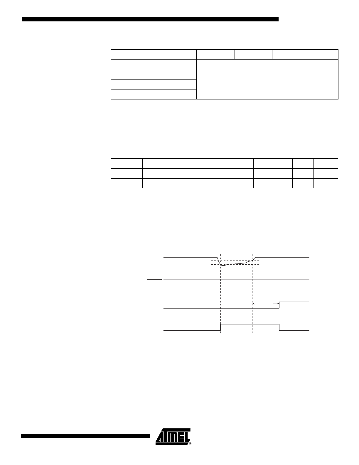
Power-on Reset A Power-on Reset (POR) pulse is generated by an On-chip detection circuit. The detec-
tion level i s defined in Table 15. Th e POR is a ctivated w heneve r V
is below the
CC
detection level. The POR circuit can be used to trigger the start-up Reset, as well as to
detect a failure in supply volt age.
A Power-on Reset (POR) circuit ensures that the device is reset from Power-on. Reaching the Power-on Reset threshold voltage invokes the delay counter, which determines
how long the device is kept in RESET after V
again, without any delay, when V
decreases below the detection level.
CC
rise. The RESET signal is activated
CC
Figure 15. MCU Start-up, RESET
V
V
CC
RESET
TIME-OUT
INTERNAL
RESET
POT
V
RST
t
TOUT
Tied to V
CC
2543A–AVR–08/03
35
Page 36

Figure 16. MCU Start-up, RESET Extended Externally
V
V
CC
RESET
TIME-OUT
INTERNAL
RESET
POT
V
RST
t
TOUT
External Reset An External Reset is generated by a low level on the RESET
pin. Reset pulses longer
than the minimum pulse width (see T able 15) will generate a rese t, even if the clock is
not running. Shorter pulses are not guarante ed to generate a reset. When the applied
signal reaches the Reset Threshold Voltage – V
counter starts the MCU after the Time-out period – t
– on its positive edge, the delay
RST
TOUT –
has expired.
Figure 17. External Reset During Operation
CC
Brown-out Detection ATtin y2313 ha s an On-chi p Brown-o ut Detecti on (BOD) cir cuit for mo nitoring the V
level during operation by comparing it to a fixed trigge r level. The trigger level for the
BOD can be selected by the BODLEVEL Fuses. The trigger level has a hysteresis to
ensure spike free Brown-out Detection. The hysteresis on the detection level should be
interpreted as V
BOT+
= V
Table 16. BODLEVEL Fuse Coding
BOT
+ V
HYST
/2 and V
(1)
BOT-
= V
BOT
- V
HYST
/2.
CC
36
ATtiny2313
BODLEVEL 2..0 Fuses Min V
111 BOD Disabled
110 1.8
100 4.3
BOT
Typ V
BOT
Max V
BOT
Units
2543A–AVR–08/03
V101 2.7
Page 37
ATtiny2313
Table 16. BODLEVEL Fuse Coding
BODLEVEL 2..0 Fuses Min V
(1)
BOT
Typ V
BOT
Max V
BOT
Units
011
010
Reserved
001
000
Note: 1. V
may be below nominal minimum operating voltage for some devices. For
BOT
devices where this is the case, the device is tested down to VCC = V
BOT
durin g the
production test. This guarantees that a Brown-Out Reset will occur before VCC drops
to a voltage where correct operation of the microcontroller is no longer guaranteed.
The test is performed using BODLEVEL = 110 for ATtiny2313V and
BODLEVEL = 101 for ATtiny2313L.
Table 17. Brown-out Characteristics
Symbol Parameter Min Typ Max Units
V
HYST
t
BOD
When the BOD is enabled, and VCC decreases to a value below the trigger level (V
Brown-out Detector Hysteresis 50 mV
Min Pulse Width on Brown-out Reset 2 ns
BOT-
in Figure 18), the Brown-out Reset is immediat ely activated. When VCC increases above
the trigger level (V
out period t
has expired.
TOUT
The BOD circuit will only detect a drop in V
for longer than t
BOD
in Figure 18), the delay cou nter starts the M CU after t he Time-
BOT+
if the voltage stays below the trigger level
CC
given in Table 15.
Figure 18. Brown-out Reset During Operation
V
CC
RESET
TIME-OUT
INTERNAL
RESET
V
BOT-
V
BOT+
t
TOUT
2543A–AVR–08/03
37
Page 38
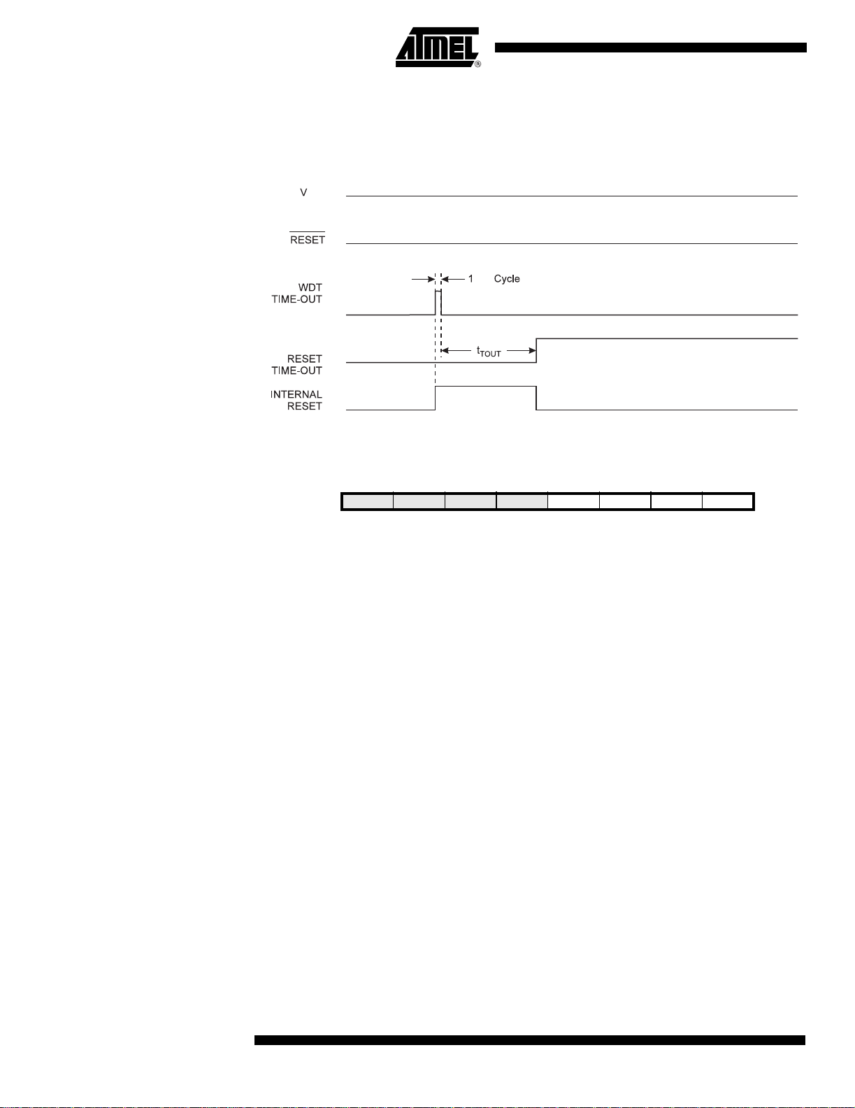
Watchdog Reset When the Watchdog times out, it will generate a short reset pul se of one CK cycle dura-
tion. On the falling edge of this puls e, the delay timer start s countin g the Time-out period
. Refer to page 45 for details on operation of the Watchdog Timer.
t
TOUT
Figure 19. Watchdog Reset During Operation
CC
CK
MCU Status Register – MCUSR
The MCU Status Register provides information on which reset source caused an M CU
reset.
Bit 76543210
– – – – WDRF BORF EXTRF PORF MCUSR
Read/Write R R R R R/W R/W R/W R/W
Initial Value 0 0 0 See B it Description
• Bit 3 – WDRF: Watchdog Reset Flag
This bit is set if a Watchdog Reset occurs. The bi t is reset by a Pow er-on Reset, or by
writing a logic zero to the flag.
• Bit 2 – BORF: Brown-out Reset Flag
This bit is set if a Brown-out Reset occurs. The bit is reset by a Powe r-on Reset, or by
writing a logic zero to the flag.
• Bit 1 – EXTRF: External Reset Flag
This bit is set i f an E xternal R eset occ urs. T he bit is reset by a Power-on Reset, or by
writing a logic zero to the flag.
• Bit 0 – PORF: Power-on Reset Flag
This bit is set if a Power-on Reset occurs. The bit is reset only by writing a logic zero to
the flag.
38
To make use of the Reset flags to identify a reset condition , the user should read and
then reset the MCUSR as early as possible in the program. If the register is cleared
before another rese t occur s, the s ourc e of the r eset can be found by examin ing the rese t
flags.
ATtiny2313
2543A–AVR–08/03
Page 39

ATtiny2313
Internal Voltage Reference
Voltage Reference Enable Signals and Start-up Time
ATtiny2313 features an internal bandgap referenc e. This re ference is used for B rownout Detection, and it can be used as an input to the Analog Comparator.
The voltage reference has a start-up time that may influence the way it should be used.
The start-up time is given i n Table 18. To s ave power, the r eference is n ot always tur ned
on. The reference is on during the follo wing situations:
1. When the BOD is enabled (by programming the BODLEVEL [2..0] Fuse).
2. When the bandgap reference is connected to th e Analog Comparat or (by set ting
the ACBG bit in ACSR).
Thus, when th e BO D is not en abled , afte r setti ng the ACB G bi t, the user m ust al ways
allow the reference to star t up befor e the output from the Analog Compar ator i s used. To
reduce power consumption in Power-down mode, the user can avoid the three conditions above to ensur e that the r efe rence is turned o ff bef ore enter ing Power -down mode.
Table 18. Internal Voltage Reference Characteristics
Symbol Parameter Condition Min Typ Max Units
V
BG
t
BG
I
BG
Bandgap reference voltage VCC = 2.7V,
Bandgap reference start-up time VCC = 2.7V,
Bandgap reference current
consumption
(1)
TA=25°C
TA=25°C
VCC = 2.7V,
TA=25°C
1.0 1.1 1.2 V
40 70 µs
15 µA
Note: 1. Values are guidelines only. Actual values are TBD.
2543A–AVR–08/03
39
Page 40
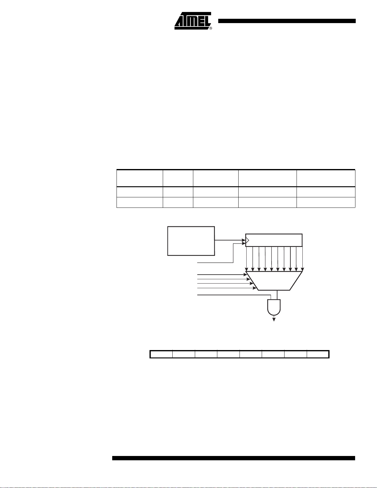
Watchdog Timer Th e Watchdog Timer is clocked from an On-chip Os cillator whic h runs at 128 kHz. By
controlling the Watchdog Timer prescaler, the Watchdog Reset interval can be adjusted
as shown in Table 21 on page 42. The WDR – Watchdog Reset – instruction resets the
Watchdog Timer value to 0. The W atchdog Ti mer is also reset when i t is disabled and
when a Chip Re set occurs. Ten different clock cycle perio ds can be selected to d etermine the reset period. If the reset period exp ires without anoth er Watchdog Rese t, the
ATtiny2313 resets and executes fr om the Reset Vector . For timing deta ils on the Watchdog Reset, refer to Table 21 on page 42.
The Wathdog Timer can also be configured to generate an interrupt instead of a reset.
This can be very helpful when using the Watchdog to wake-up from Power-down.
To prevent unintentional disabling of the Watchdog or unintentional change of time-out
period, two different safety l evels are sele cted by the f use WDTO N a s shown in Tabl e
19. Refer to “Timed Sequences for Changing the Configuration of the Watchdog Timer”
on page 44 for details.
Table 19. WDT Configuration as a Function of the Fuse Settings of WDTON
Watchdog Timer Control Register – WDTCR
WDTON
Safety
Level
WDT Initial
State
How to Disable the
WDT
How to Change
Time-out
Unprogrammed 1 Disabled Timed sequence No limitations
Programmed 2 Enabled Always enabled Timed sequence
Figure 20. Watchdog Timer
OSC/2K
OSC/4K
WATCHDOG
PRESCALER
OSC/8K
OSC/16K
OSC/32K
MCU RESET
OSC/64K
OSC/128K
OSC/512K
OSC/256K
OSC/1024K
128 kHz
OSCILLATOR
WATCHDOG
RESET
WDP0
WDP1
WDP2
WDP3
WDE
Bit 76543210
WDIF WDIE W DP3 WDCE WDE WD P2 WDP1 WDP0 WDTCR
Read/Write R/W R/W R/W R/W R/W R/W R/W R/W
Initial Value 0 0 0 0 X 0 0 0
40
• Bit 7 – WDIF: Watchdog Timeout Interrupt Flag
This bit is set when a time-out occurs in the Watchdog Timer and the Watch dog Timer is
configured for int err upt. WDIF i s clear ed by hard ware when execut ing t he corres ponding
interrupt handling vect or. Alt ernati vely, WDIF is cleared by wri ting a logic one to the flag.
When the I-bit in SREG and WDIE are set, the Watchdog Time-out Interrupt is
executed.
ATtiny2313
2543A–AVR–08/03
Page 41

ATtiny2313
• Bit 6 – WDIE: Watchdog Timeout Interrupt Enable
When this bit is written to one, WDE is cleared, and the I-bit in the Sta tus Regist er is set ,
the Watchdog Time-out Interrupt is enabled. In this mode the corresponding interrupt is
executed instead of a reset if a time out i n the Watchdog Timer occurs.
If WDE is set, WDIE is automatically cleared by hardware when a time-out occurs. This
is useful for keeping the Watchdog Reset security while using the interrupt. After the
WDIE bit is cleared, the next time-out will generate a reset. To avoid the Watchdog
Reset, WDIE must be set after each interrupt.
Table 20. Watchdog Timer Configuration
WDE WDIE Watchdog Timer State Action on Time-out
0 0 Stopped None
0 1 Running Interrupt
1 0 Running Reset
1 1 Running Interrupt
• Bit 4 – WDCE: Watchdog Change Enable
This bit must be set when the WDE bit is written to logic zero. Otherwise, the Watchdog
will not be disabled. Once written to one, hardware will clear this bit after four clock
cycles. Refer to the description of the WDE bit for a Watchdog disable procedure. This
bit must also be set when changing the prescaler bits. See “Timed Sequences for
Changing the Configuration of the Watchdog Timer” on page 44.
• Bit 3 – WDE: Watchdog Enable
When WDE is written to logic one, th e Watchdog Timer i s enabled, and if WDE is writt en
to logic zero, the Watchdog Timer function is disabled. WDE can only be cleared if the
WDCE bit has logic level one. To disabl e an enabled Watchdog T imer, the fo llowing pro cedure must be followed:
1. In the same operation, write a logic one to WDCE and WDE. A logic one must be
written to WDE even though it is set to one before the disable operation starts.
2. Within the next four clock cycles, write a logic 0 to WDE. This disables the
Watchdog.
In safety level 2, it is not possible t o disable the Watchdog Timer, even w ith the algorithm describe d abov e. See “Time d Seque nces for Cha nging the Configu ration of the
Watchdog Timer” on page 44.
In safety level 1, WDE is overridden by WDRF in MCUSR. See “MCU Status Register –
MCUSR” on page 38 for description of WDRF. This means that W DE is always set when
WDRF is set. To clear WDE, WDRF must be cleared before disabling the Watchdog
with the procedure described above. This feature ensures multiple resets during conditions causing failure, and a safe start-up after the failure.
Warning:If the watchdog timer is not be used in the application, it is important to go through a
watchdog disable procedu re in the initialization of the device. I f the Watchd og is acci den tally enabled, for examp le by a r unawa y pointe r or b rown-out co ndition , the de vice will be
reset, which in turn will lead to a new watchdog reset. T o avoid th is situation, the app lication software should always clear the WDRF flag and the WDE control bit in the
initialization routine.
2543A–AVR–08/03
41
Page 42

• Bits 5, 2..0 – WDP3..0: Watchdog Timer Prescaler 3, 2, 1, and 0
The WDP3..0 bits determine the Watchdog Timer prescaling when the Watchdog Timer
is enabled. The differ ent prescaling values and t heir corresponding Timeout Periods are
shown in Table 21.
Table 21. Watchdog Timer Prescale Select
Number of WDT Oscillator
WDP3 WDP2 WDP1 WDP0
0000 2K cycles 16 ms
0001 4K cycles 32 ms
0010 8K cycles 64 ms
0011 16K cycles 0.125 s
0100 32K cycles 0.25 s
0101 64K cycles 0.5 s
0110 128K cycles 1.0 s
0111 256K cycles 2.0 s
1000 512K cycles 4.0 s
1001 1024K cycles 8.0 s
1010
1011
1100
1101
1110
1111
Cycles
Reserved
Typical Time-out at
VCC = 5.0V
42
ATtiny2313
2543A–AVR–08/03
Page 43

ATtiny2313
The following code example shows one assembly and one C function for turning off the
WDT. The example assumes that interrupts are controlled (e.g., by disabling interrupts
globally) so that no interrupt s wil l occur during execution of these functions.
Assembly Code Example
WDT_off:
WDR
; Clear WDRF in MCUSR
ldi r16, (0<<WDRF)
out MCUSR, r16
; Write logical one to WDCE and WDE
; Keep old prescaler setting to prevent unintentional Watchdog Reset
in r16, WDTCR
ori r16, (1<<WD CE)|(1<<WDE)
out WDTCR, r16
; Turn off WDT
ldi r16, (0<<WD E)
out WDTCR, r16
ret
C Code Example
void WDT_off(void)
{
_WDR();
/* Clear WDRF in MCUSR */
MCUSR = 0x00;
/* Write logical one to WDCE and WDE */
WDTCR |= (1<<WDCE) | (1<<WDE);
/* Turn off WDT */
WDTCR = 0x00;
}
(1)
(1)
2543A–AVR–08/03
Note: 1. The example code assumes that the part specific header file is included.
43
Page 44

Timed Sequences for
Changing the
The sequence for changing configuration differs slightly between the two safety levels.
Separate procedures are described for each level.
Configuration of the
Watchdog Timer
Safety Level 1 In this mode, the Watchdog Timer is initially disabled, but can be enabled by writing the
WDE bit to one without any restriction. A timed sequence is needed when disabling an
enabled Watchdog Timer. To disable an enabled Watchdog Timer, the following procedure must be followed:
1. In the same operation, write a logic one to WDCE and WDE. A logic one must be
written to WDE regardless of the previous value of the WDE bit.
2. Within the next four clock cycles, in the same operation, write the WDE and
WDP bits as desired, but with the WDCE bit cleared.
Safety Level 2 In this mode, the Watchdog Timer is always enabled, and the WDE bit will always read
as one. A timed sequence is needed when changing the Watchdog Time-out period. To
change the Watchdog Time-out, the followi ng procedure must be followed:
1. In the same operation, write a logical one to WDCE and WDE. Even though the
WDE always is set, the WDE must be written to one to start the timed sequence.
2. Within the next four clock cycles, in the same operat ion, write the WDP bits as
desired, but with the WDCE bit cleared. The value written to the WDE bit is
irrelevant.
44
ATtiny2313
2543A–AVR–08/03
Page 45

ATtiny2313
Interrupts This section describes the specifics of the interrupt han dling as performed in
ATtiny2313. For a general explanat ion of the AVR inter rupt handlin g, re fer to “Reset and
Interrupt Handling” on page 10.
Interrupt Ve ctors in ATtiny2313
Table 22. Reset and Interrupt Vectors
Vector
No.
10 0x0009 USART0, TX USART0, Tx Complete
11 0x000A ANALOG COMP Analog Comparator
12 0x000B PCINT Pin Change Interrupt
13 0x000C TIMER1 COMPB Timer/Counter1 Compare Match B
14 0x000D TIMER0 COMPA Timer/Counter0 Compare Match A
15 0x000E TIMER0 COMPB Timer/Counter0 Compare Match B
16 0x000F USI START USI Start Condition
Program
Address Sourc e Inter rupt Definition
1 0x0000 RESET External Pin, Power-on Reset, Brown-out Reset,
and Watchdog Reset
2 0x0001 INT0 External Interrupt Request 0
3 0x0002 INT1 External Interrupt Request 1
4 0x0003 TIMER1 CAPT Timer/Counter1 Capture Event
5 0x0004 TIMER1 COMPA Timer/Counter1 Compare Match A
6 0x0005 TIMER1 OVF Timer/Counter1 Overflow
7 0x0006 TIMER0 OVF Timer/Counter0 Overflow
8 0x0007 USART0 , RX USART0, Rx Complete
9 0x0008 USART0, UDRE USART0 Data Register Empty
2543A–AVR–08/03
17 0x0010 USI OVERFLOW USI Overflow
18 0x0011 EE READY EEPROM Ready
19 0x0012 WDT OVERFLOW Watchdog Timer Overflow
45
Page 46

The most ty pical and gene ral program se tup for the Re set and Interru pt Vector
Addresses in ATtiny2313 is:
Address Labels Code Comments
0x0000 rjmp RESET ; Reset Handler
0x0001 rjmp INT0 ; External Interrupt0 Handler
0x0002 rjmp INT1 ; External Interrupt1 Handler
0x0003 rjmp TIM1_C APT ; Timer1 Capture Handler
0x0004 rjmp TIM1_COMPA ; Timer1 CompareA Handler
0x0005 rjmp TIM1_OVF ; Timer1 Overflow Handler
0x0006 rjmp TIM0_OVF ; Timer0 Overflow Handler
0x0007 rjmp USART0 _RXC ; USART0 RX Complete Handler
0x0008 rjmp USART0_DRE ; USART0,UDR Empty Handler
0x0009 rjmp USART0 _TXC ; USART0 TX Complete Handler
0x000A rjmp ANA_CO MP ; Analog Comparat or Handler
0x000B rjmp PCINT ; Pin Change Interrupt
0x000C rjmp TIMER1 _COMPB ; Timer1 Compare B Hand ler
0x000D rjmp TIMER0 _COMPA ; Timer0 Compare A Hand ler
0x000E rjmp TIMER0 _COMPB ; Timer0 Compare B Hand ler
0x000F rjmp USI_ST ART ; Usi Start Handler
0x0010 rjmp USI_OVERFLOW ; USI Overflow Handler
0x0011 rjmp EE_READY ; EEPROM Ready Handler
0x0012 rjmp WDT_OVERFLOW ; Watchdog Overflow Handler
;
0x0013 RESET: ldi r16, low(RAMEND) ; Main program start
0x0014 out SPL,r16 Set Stack Pointer to top of RAM
0x0015 sei ; Enable interrupts
0x0016 <instr> xxx
... ... ... ...
46
ATtiny2313
2543A–AVR–08/03
Page 47
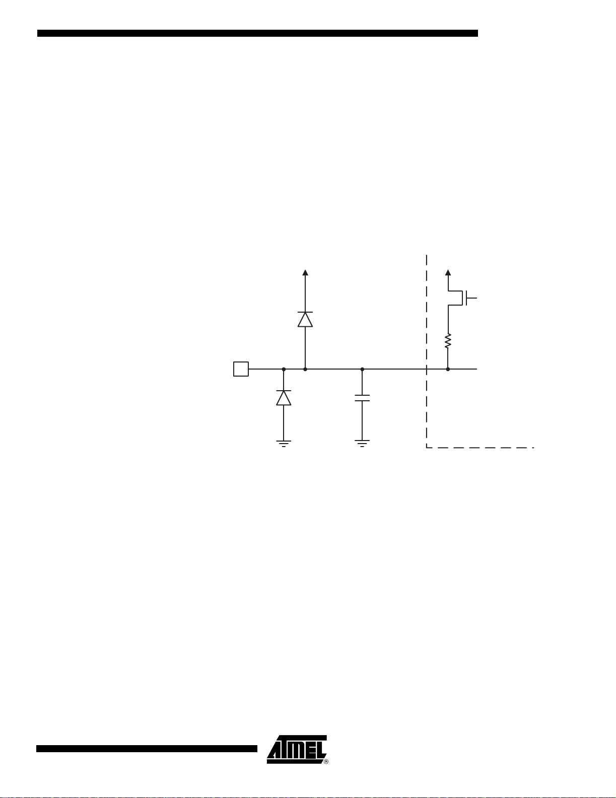
ATtiny2313
I/O-Ports
Introduction All AVR ports have true Read-Modify-Write functionality when used as general digital
I/O ports. This means that the direction of one port pin can be changed without unintentionally chang ing the direc tion of any ot her pin with the SBI and CBI instruc tions. The
same applies when changing drive value (if configured as output) or enabling/disabling
of pull-up resistors (if configured as input). Each output buffer has symmetrical drive
characteristics with both high si nk and source capability. The pin driver is strong enough
to drive LED displays directly. All port pins have individually selectable pull-up resistors
with a supply-voltage invariant resistance. All I/O pins have protection diodes to both
and Ground as indicated in Figure 21. Refer to “Electrical Characteristics” on page
V
CC
178 for a complete list of parameters.
Figure 21. I/O Pin Equivalent Schematic
R
pu
Pxn
C
pin
All registers and bit references in this section are written in general form. A lower case
“x” represents the numbering letter for the port, and a lower case “n” represents the bit
number. However, when using the register or bit defines in a program, the precise form
must be used. For example, PORTB3 for bit no. 3 in Port B, here documented generally
as PORTxn. The physical I/O Registers and bit locations are listed in “Register Description for I/O-Port s” on page 60.
Three I/O memory address locations are allocated for each port, one each for the Data
Register – PORTx, Data Direction Regist er – DDRx, and the Port Input Pin s – PINx. The
Port Input Pins I/O location is read only, while the Data Register and the Data Direction
Register are read /write. Howev er, w riting a log ic one to a bit in the P INx Re gister, w ill
result in a toggle in the corresponding bit in the Data Re gister. In addition, the Pull-up
Disable – PUD bit in MCUCR di sables the pull-up function for all pins in all ports when
set.
See Figure
"General Digital I/O" for
Logic
Details
2543A–AVR–08/03
Using the I/O port as General Digital I/O is described i n “Ports as General Digital I/O” on
page 48. Most p ort pins are multiplexed w ith alternate f unctions for the peripheral features on the device. How each alt ernate function interfe res wi th the port pin is described
in “Alternate Port Func tions” on pag e 52. Refe r to the indivi dual modu le sec tions for a
full description of the alternate functions.
47
Page 48

Note that enabling the al ternate function of some of the port pins does not aff ect the use
of the other pins in the port as general digital I/O.
Ports as General Digital I/O
The ports are bi-directional I/O ports with o ptional internal pull-up s. Figure 22 sh ows a
functional description of one I/O-port pin, here generically called Pxn.
Figure 22. General Digital I/O
Pxn
(1)
SLEEP
SYNCHRONIZER
DLQ
D
PINxn
Q
PUD
Q
D
DDxn
Q
CLR
RESET
Q
D
PORTxn
Q
CLR
RESET
Q
Q
RRx
WDx
RDx
RPx
1
0
WPx
WRx
DATA BUS
clk
I/O
PUD: PULLUP DISABLE
SLEEP: SLEEP CONTROL
clk
: I/O CLOCK
I/O
WDx: WRITE DDRx
RDx: READ DDRx
WRx: WRITE PORTx
RRx: READ PORTx REGISTER
RPx: READ PORTx PIN
WPx: WRITE PINx REGISTER
Note: 1. WRx, WPx, WDx, RRx, RPx, and RDx are common to all pins within the same port.
clk
, SLEEP, and PUD are common to all ports.
I/O
Configuring the Pin Each p ort pin co nsists of three regi ster b its: D Dxn, P ORTx n, an d PIN xn. As s hown in
“Register Description for I/O-Ports ” on pag e 60, the DDxn bits are ac cessed at the
DDRx I/O ad dress, the P ORTx n bits a t the PO RTx I/O address , an d the P INx n bi ts at
the PINx I/O address.
The DDxn bit in the DDRx Register selects the direction of this pin. If DDxn is written
logic one, Pxn is confi gured as an output pin. If DDxn is written logic zero, Pxn is configured as an input pin.
If PORTx n is w ritten logic one wh en th e pin is confi gured as an input pin, th e pul l-up
resistor is acti vated. To switch th e pull-up resis tor off , POR Txn h as to b e wr itten logic
zero or the pin has to be configured as an output pin. The port pins are tri-stated when
reset condition becomes acti ve, even if no clocks are running.
If PORTxn is written logic one when the pin is configured as an output pin , the port pin is
driven high (one). If PORTxn is written logic zero when the pin is configured as an output pin, the port pin is driven low (zero).
48
ATtiny2313
2543A–AVR–08/03
Page 49
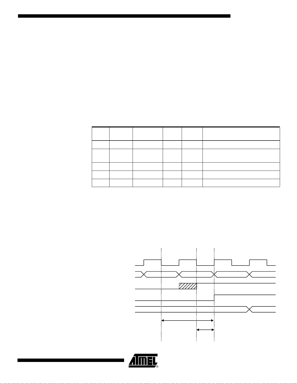
ATtiny2313
Toggling the Pin Writing a logic one to PINxn toggles the value of PORTxn, independent on the value of
DDRxn. Note that the SBI instruction can be used to toggle one single bit in a port.
Switching Between Input and Output
When switching bet ween tri-stat e ({DD xn, PO RTxn} = 0 b00) an d out put hi gh ({DDxn,
PORTxn} = 0b11), an intermediate state with either pull-up enabled {DDxn, PORTxn} =
0b01) or output low ({DDxn, PORTxn} = 0b10 ) must occur. Normally, the pull-up
enabled state is fully acceptable, as a high-impedant environment will not notice the difference between a strong high driver and a pull-up. If this is not the case, the PUD bit in
the MCUCR Register can be set to disable all pull-ups in all ports.
Switching between input with pull-up and output low generates the same problem. The
user must use either the tri-state ({DDxn, PORTxn} = 0b00) or the output high state
({DDxn, PORTxn} = 0b11) as an intermediate step.
Table 23 summarizes the control signa ls for the pin value.
Table 23. Port Pin Configurations
PUD (in
DDxn PORTxn
0 0 X Input No Tri-state (Hi-Z)
0 1 0 Input Yes
0 1 1 Input No Tri-state (Hi-Z)
1 0 X Output No Output Low (Sink)
1 1 X Output No Output High (Source)
MCUCR2) I/O Pull-up Comment
Pxn will source current if ext. pulled
low.
Reading the Pin Value Independent of the setting of Data Direction bit DDxn, the port pin can be read through
the PINxn Register bit. As shown in Figure 22, the PI Nxn Register bit and the preceding
latch constitute a synchronizer. This is needed to avoid metastability if the physical pin
changes value near the edge of the internal clock, but it also introduces a delay. Figure
23 shows a t iming dia gram of th e syn chronizat ion w hen readi ng an extern ally a pplie d
pin value. The maximum and minimum propagation delays are denoted t
pd,max
and t
pd,min
respectively.
Figure 23. Synchronization when Reading an Externally Applied Pin value
SYSTEM CLK
INSTRUCTIONS
XXX in r17, PINx
XXX
SYNC LATCH
PINxn
r17
0x00 0xFF
t
pd, max
t
pd, min
2543A–AVR–08/03
49
Page 50

Consider the clock period starting shortly after the first falling edge of the system clock.
The latch is closed when the clock is low, and goes transparent when the clock is high,
as indicated by the shaded region of the “SYNC LATCH” signal. The signal value is
latched when the system clock goes l ow. It i s clocked into the PI Nxn Registe r at the succeeding positive clock edge. As indicated by the two arrows tpd,max and tpd,min, a
single signal tra nsition on the pin wi ll be delayed betwe en ½ and 1½ system clock
period depending upon the time of assertion.
When reading back a software assigned pin value , a nop instruc tion must be in serted as
indicated in Figure 24. The out instruc ti on sets the “SYNC LATCH” signal at the positive
edge of the clock. In this case, the delay tpd through the synchronizer is 1 system clock
period.
Figure 24. Synchronization when Reading a Software Assigned Pin Value
SYSTEM CLK
r16
INSTRUCTIONS
SYNC LATCH
PINxn
r17
0xFF
out PORTx, r16 nop in r17, PINx
0x00 0xFF
t
pd
50
ATtiny2313
2543A–AVR–08/03
Page 51

ATtiny2313
The following code example shows how to set port B pins 0 and 1 high, 2 and 3 low, and
define the port pins from 4 to 7 as input with pull-ups assigned to port pins 6 and 7. The
resulting pin values are read back again, but as previously discussed, a nop instruct ion
is included to be able to read back the value recently assigned to some of the pins.
Assembly Code Example
...
; Define pull-ups and set outputs high
; Define directions for port pins
ldi r16,(1<<PB7)|(1<<PB6)|(1<<PB1)|(1<<PB0)
ldi r17,(1<<DDB3)|(1<<DDB2)|(1<<DDB1)|(1<<DDB0)
out PORTB,r16
out DDRB,r17
; Insert nop for synchronization
nop
; Read port pins
in r16,PINB
...
(1)
C Code Example
unsigned char i;
...
/* Define pull-ups and set out puts high */
/* Define directions for port pins */
PORTB = (1<<PB7)|(1<<PB6)|(1<<PB1)|(1<<PB0);
DDRB = (1<<DDB3)|(1<<DDB2)|(1<<DDB1)|(1<<DDB0);
/* Insert nop for synchroni zation*/
_NOP();
/* Read port pins */
i = PINB;
...
Digital Input Enable and Sleep Modes
2543A–AVR–08/03
Note: 1. For the assembly program, two temporary registers are used to minimize the time
from pull-ups are set on pins 0, 1, 6, and 7, until the direction bits are correctly set,
defining bit 2 and 3 as low and redefining bits 0 and 1 as strong high drivers.
As shown in Figure 22, the digital input signal can be clamped to ground at the input of
the schmitt-trigger. The signal denoted SLE EP in the figure, is set by the MCU Sle ep
Controller in Power-down mode, and Standby mode to avoid high power consumption if
some input signals are left floating, or have an analog signal level close to V
CC
/2.
SLEEP is overridden for port pins enabled as ex ter nal interr upt pins . If the external inter rupt request i s not enab led, SLEE P is active also for these pins. SLEEP i s also
overridden by various other alternate functions as described in “Alternate Port Functions” on page 52.
If a logic high level (“one”) is present on an asynchronous external interrupt pin configured as “Interrupt on Rising Edge, Falling Edge, or Any Logic Change on Pin” while the
external interru pt is not enab led, the co rrespond ing Extern al Interru pt Flag will be set
when resuming from the above mentioned Sleep mode, as the clamping in these sleep
mode produces the requested logic change.
51
Page 52
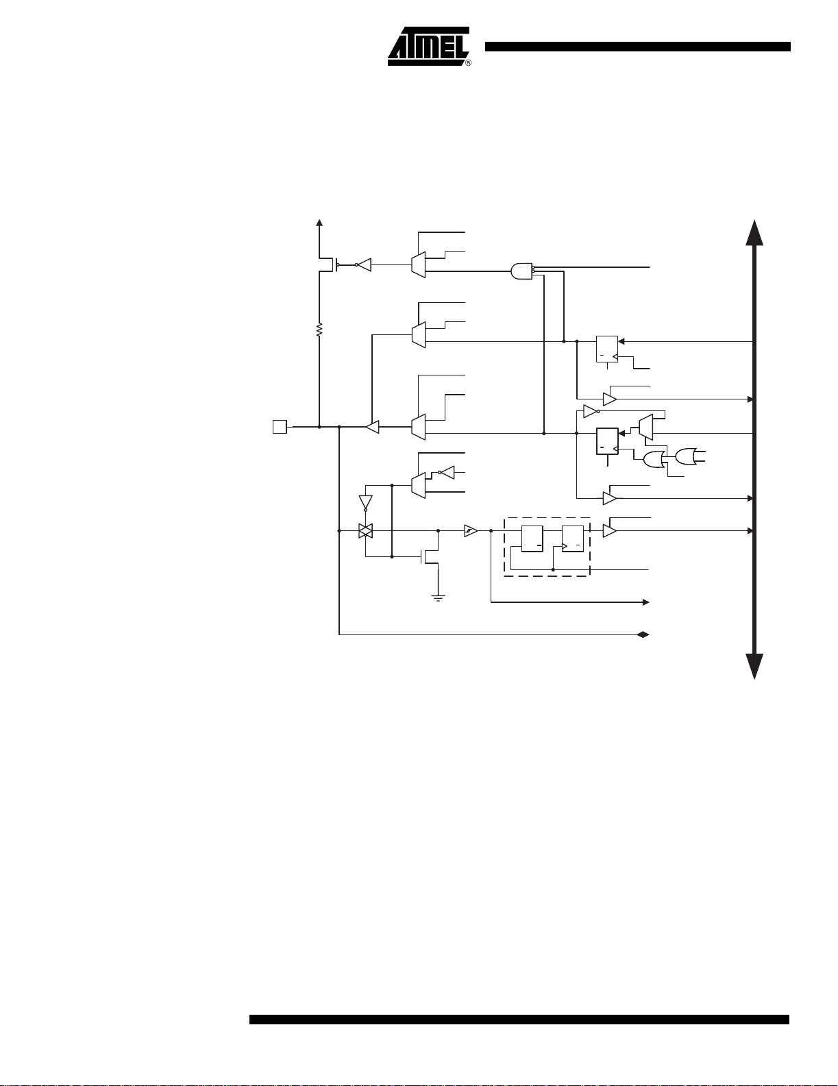
Alternate Po r t Func tions Most port pins have alternate functions in add ition to being ge neral digital I/O s. Figure
25 shows how the port pin control signals from the simplified Figure 22 can be overridden by alternate functions . The overri ding si gnals may no t be present in all port pi ns, but
the figure serves as a generic d escription ap plicable to al l port pins in the A VR m icrocontroller family.
Figure 25. Alternate Port Functions
1
0
1
0
Pxn
1
0
1
0
(1)
PUOExn
PUOVxn
DDOExn
DDOVxn
PVOExn
PVOVxn
DIEOExn
DIEOVxn
SLEEP
SYNCHRONIZER
SET
DLQ
D
PINxn
Q
CLR
PUD
D
Q
DDxn
Q
CLR
RESET
D
Q
PORTxn
Q
CLR
RESET
Q
Q
CLR
1
0
WDx
RDx
RRx
RPx
clk
PTOExn
WPx
WRx
I/O
DATA BUS
DIxn
AIOxn
PUOExn: Pxn PULL-UP OVERRIDE ENABLE
PUOVxn: Pxn PULL-UP OVERRIDE VALUE
DDOExn: Pxn DATA DIRECTION OVERRIDE ENABLE
DDOVxn: Pxn DATA DIRECTION OVERRIDE VALUE
PVOExn: Pxn PORT VALUE OVERRIDE ENABLE
PVOVxn: Pxn PORT VALUE OVERRIDE VALUE
DIEOExn: Pxn DIGITAL INPUT-ENABLE OVERRIDE ENABLE
DIEOVxn: Pxn DIGITAL INPUT-ENABLE OVERRIDE VALUE
SLEEP: SLEEP CONTROL
PTOExn: Pxn, PORT TOGGLE OVERRIDE ENABLE
PUD: PULLUP DISABLE
WDx: WRITE DDRx
RDx: READ DDRx
RRx: READ PORTx REGISTER
WRx: WRITE PORTx
RPx: READ PORTx PIN
WPx: WRITE PINx
clk
: I/O CLOCK
I/O
DIxn: DIGITAL INPUT PIN n ON PORTx
AIOxn: ANALOG INPUT/OUTPUT PIN n ON PORTx
Note: 1. WRx, WPx, WDx, RRx, RPx, and RDx are common to all pins within the same port.
clk
, SLEEP, and PUD a re co mmo n to all ports. A ll othe r sign als ar e un i que f or e ach
I/O
pin.
Table 24 su mmariz es the funct ion of the ove rriding signals. T he pin an d port indexe s
from Figure 25 are not shown in the succeeding tables. The overriding signals are generated internally in the modules having the alternate function.
52
ATtiny2313
2543A–AVR–08/03
Page 53

ATtiny2313
Table 24. Generic Description of Overridi ng Signal s for Alternate Functions
Signal Name Full Name Description
PUOE Pull-up Override
Enable
PUOV Pull-up Override
Value
DDOE Data Direction
Override Enable
DDOV Data Direction
Override Value
PVOE Port Value
Override Enable
PVOV Port Value
Override Value
PTOE Port Toggle
Override Enable
DIEOE Digital Input
Enable Override
Enable
DIEOV Digital Input
Enable Override
Value
If this signal is set, the pull-up enable is controlled by the
PUOV signal. If this signal is cleared, the pull-up is
enabled when {DDxn, PORTxn, PUD} = 0b010.
If PUOE is set, the pull-up is enabled/disabled when
PUOV is set/cleared, regardless of the setting of the
DDxn, PORTxn, and PUD Register bits.
If this signal is set, the Output Driver Enable is controlled
by the DDOV signal. If this signal is cleared, the Output
driver is enabled by the DDxn Register bit.
If DDOE is set, the Output Driver is enabled/disabled
when DDOV is set/cleared, regardless of the setting of
the DDxn Register bit.
If this signal is set and the Output Driver is enabled, the
port value is controlled by the PVOV signal. If PVOE is
cleared, and the Output Driver is enabled, the port Value
is controlled by the PORTxn Register bit.
If PVOE is set, the port value is set to PVOV, regardless
of the setting of the PORTxn Register bit.
If PTOE is set, the PORTxn Register bit is inverted.
If this bit is set, the Digital Input Enable is controlled by
the DIEOV signal. If t his signal i s clear ed, the Digital Input
Enable is dete rmined by MCU sta te ( Norm al m ode , sl ee p
mode).
If DIEOE is set, the Digital Input is enabled/disabled
when DIEOV is set/cleared, regardless of the MCU state
(Normal mode, sleep mode).
2543A–AVR–08/03
DI Digital Input This is the Digital Input to alternate functions. In the
figure, the signal is connected to the output of the schmitt
trigger but before the synchronizer. Unless the Digital
Input is used as a clock source, the module with the
alternate function will use its own synchronizer.
AIO Analog
Input/Output
This is the Analog Input/output to/from alternate
functions. The signa l is conn ected dire ctly to t he pad, a nd
can be used bi-directionally.
The following subsections shortly describe the alternate functions for each port, and
relate the overriding signals to the alternate function. Refer to the alternate function
description for further details.
53
Page 54

MCU Control Register – MCUCR
Bit 7 6 5 4 3 2 1 0
PUD
Read/Write R/W R/W R/W R/W R/W R/W R/W R/W
Initial Value 0 0 0 0 0 0 0 0
SM1 SE SM0 ISC11 ISC10 ISC01 ISC00 MCUCR
• Bit 7 – PUD: Pull -u p D is a b le
When this bit is written to one, the pull-ups in the I/O ports are disabled even i f the DDxn
and PORTxn Registers are configured to enable the pull- ups ({DDxn, PORTxn} = 0b01).
See “Configuring the Pin” on page 48 for more details about this feature.
Alternate Functions of Port A The Port A pins with alternate functions are as shown in Table 5.
Table 25. Port A Pins Alternate Functions
Port Pin Alternate Fu nction
PA2 RESET, dW
PA1 XTAL2
PA0 XTAL1
Alternate Functions of Port B The Port B pins with alternate functions are shown in Table 26.
Table 26. Port B Pins Alternate Functions
Port Pin Alternate Functions
PB7 USCK/SCL/PCINT7
PB6 DO/PCINT6
PB5 D I/SDA/PCINT5
PB4 OC1B/PCINT4
PB3 OC1A/PCINT3
PB2 OC0A/PCINT2
PB1 AIN1/PCINT1
PB0 AIN0/PCINT0
The alternate pin configur ati on is as follows:
• USCK/SCL/PCINT7 - Port B, Bit 7
USCK: Three-wire mode Universal Serial Interfac e Clock.
SCL: Two-wire mode Serial Clock for USI Two-wire mode.
PCINT7: Pin Change Interrupt source 7. The PB7 pin can serve as an external interrupt
source.
• DO/PCINT6 - Port B, Bit 6
DO: Three-wire mode Universal Serial I nte rface Dat a output . Three- wire mode Dat a output overrides PORTB6 value and it is driven to the port when data direction bit DDB6 is
set (one). However the PORTB6 bit still controls the pull-up enabling pull-up, if direction
is input and PORTB6 is set (one).
54
ATtiny2313
2543A–AVR–08/03
Page 55

ATtiny2313
PCINT6: Pin Change Interrupt Sour ce 6. The PB6 pin can serve as an external in terrupt
source.
• DI/SDA/PCINT5 - Port B, Bit 5
DI: Three-wire mode Un iversal Serial Inte rface Data in put. Three -wire mode does not
override norma l po rt functi ons, so pin mus t be co nfigu red as an input. SDA: Two -wire
mode Serial Interface Data.
PCINT5: Pin Change Interrupt Sour ce 5. The PB5 pin can serve as an external in terrupt
source.
• OC1B/PCINT4 – Port B, Bit 4
OC1B: Output Comp are Match B output: The PB4 pin can serve as an e xternal output
for the Timer/Coun ter1 Output C ompa re B . The p in h as to be conf igured a s an o utput
(DDB6 set (one)) to s erv e this f uncti on. The OC1B pi n is al so the out put pin for th e PWM
mode timer function.
PCINT4: Pin Change Interrupt Sour ce 4. The PB4 pin can serve as an external in terrupt
source.
• OC1A/PCINT3 – Port B, Bit 3
OC1A: Output Comp are Match A output: The PB3 pin can serve as an e xternal output
for the Timer/Coun ter1 Output C ompa re A . The p in h as to be conf igured a s an o utput
(DDB3 set (one)) to s erv e this f uncti on. The OC1A pi n is al so the out put pin for th e PWM
mode timer function.
PCINT3: Pin Change Interrupt Sour ce 3: The PB3 pin can serve as an external in terrupt
source.
• OC0A/PCINT2 – Port B, Bit 2
OC0A: Output Comp are Match A output. The PB2 pin can serve as an e xternal output
for the Timer/Coun ter0 Output C ompa re A . The p in h as to be conf igured a s an o utput
(DDB2 set (one)) to s erv e this f uncti on. The OC1A pi n is al so the out put pin for th e PWM
mode timer function.
PCINT2: Pin Change Interrupt Sour ce 2. The PB2 pin can serve as an external in terrupt
source.
2543A–AVR–08/03
55
Page 56

• AIN1/PCINT1 – Port B, Bit 1
AIN1: Ana log Co mp arator N egat iv e inpu t and ADC 6: ADC in put cha nnel 6
. Configure
the port pin as input with the internal pul l-up switc hed off to avoid the di gital port func tion
from interfering with t he function of the analog comparator or analog to digital converter.
PCINT1: Pin Change Interrupt Sour ce 1. The PB1 pin can serve as an external in terrupt
source.
• AIN0/PCINT0 – Port B, Bit 0
AIN0: Analog Comparator Positive input and ADC5: ADC input channel 5
. Configure the
port pin as in put w ith the in tern al pu ll-up swi tched off to a voi d the dig ital port fu nc tion
from interfering with the function of the Analog Comparator or analog to digital
converter.
PCINT0: Pin Change Interrupt Sour ce 0. The PB0 pin can serve as an external in terrupt
source.
Table 27 and Table 28 relate the alternate funct ions of Port B to the ove rriding signals
shown in Figure 25 on page 52. SPI MSTR INPUT and SPI SLAVE OUTPUT constitute
the MISO signal, while MOSI is divided into SPI MSTR OUTPUT and SPI SLAVE
INPUT.
Table 27. Overriding Signals for Alternate Funct ions in PB7..PB4
Signal
Name
PUOE 0 0 0 0
PB7/USCK/
SCL/PCINT7 PB6/DO/PCINT6
PB5/SDA/
DI/PCINT5
PB4/OC1B/
PCINT4
PUOV 0 0 0 0
DDOE USI_TWO_WIRE 0 USI_TWO_WIRE 0
DDOV (USI_SCL_HOLD
+ PORTB7)•DDB7
PVOE USI_TWO_WIRE
• DDRB7
PVOV 0 DO 0 0OC1B_PVOV
PTOE USI_PTOE 0 0 0
DIEOE (PCINT7•PCIE)
+USISIE
DIEOV 1 1 1 1
DI PCINT7 INPUT
USCK INPUT SCL
INPUT
AIO – – – –
0(SDA + PORTB5)•
DDRB5
USI_THREE_WIRE USI_TWO_WIRE
• DDRB5
(PCINT6•PCIE) (PCINT5•PCIE) +
USISIE
PCINT6 INPUT PCINT5 INPUT
SDA INPUT
DI INPUT
0
OC1B_PVOE
(PCINT4•PCIE)
PCINT4 INPUT
56
ATtiny2313
2543A–AVR–08/03
Page 57

Table 28. Overriding Signals for Alternate Funct ions in PB3..PB0
ATtiny2313
Signal
Name
PUOE 0 0 0 0
PUOV 0 0 0 0
DDOE 0 0 0 0
DDOV 0 0 0 0
PVOE OC1A_PVOE OC0A_PVOE 0 0
PVOV OC1A_PVOV OC0A_PVOV 0 0
PTOE 0 0 0 0
DIEOE (PCINT3 • PCIE) (PCINT2 • PCIE) (PCINT1 • PCIE) (PCINT0 • PCIE)
DIEOV 1 1 1 1
DI PCINT7 IN PUT PCINT6 INPUT PCINT5 INPUT PCINT4 INPUT
AIO – – AIN1 AIN0
PB3/OC1A/
PCINT3
PB2/OC0A/
PCINT2
PB1/AIN1/
PCINT1
Alternate Functions of Port D The Port D pins with alternate functions are shown in Table 29.
Table 29. Port D Pins Alternate Functions
Port Pin Alternate Function
PD6 ICP
PD5 OC0B/T1
PB0/AIN0/
PCINT0
PD4 T0
PD3 INT1
PD2 INT0/XCK/CKOUT
PD1 TXD
PD0 RXD
The alternate pin configur ati on is as follows:
• ICP – Port D, Bit 6
ICP: Timer/Counter1 Input Capture Pin. The PD6 pin can act as an Input Capture pin for
Timer/Counter1
• OC1B/T1 – Port D, Bit 5
OC0B: Output Compare Match B out put: The PD5 pi n can serve as an external o utput
for the Timer/Coun ter0 Output C ompa re B . The p in h as to be conf igured a s an o utput
(DDB5 set (one)) to s erv e this f uncti on. The OC0B pi n is al so the out put pin for th e PWM
mode timer function.
T1: Timer/Counter1 External Counter Clock input is enabled by setting (one) the bits
CS02 and CS01 in the Timer/Counter1 Control Register (TCCR1).
2543A–AVR–08/03
57
Page 58

• T0 – Port D, Bit 4
CKOUT: System Clock Output
T0: Timer/Counter0 External Counter Clock input is enabled by setting (one) the bits
CS02 and CS01 in the Timer/Counter0 Control Register (TCCR0).
• INT1 – Port D, Bit 3
INT0: External Interrupt Source 0. The PD3 pin can serve as an external interrupt
source to the MCU.
• INT0/XCK/CKOUT – Port D, Bit 2
INT1: External Interrupt Source 1. The PD2 pin can serve as en axternal interrupt
source to the MCU.
XCK: USART Transfer Clock used only by Synchronous Transfer mode.
CKOUT: System Clock Output
• TXD – Port D, Bit 1
TXD: UART Data Transmitter.
• RXD – Port D, Bit 0
RXD: UART Data Receiver.
Table 30 and Table 31 relates the alternate functions of Port D to the overriding signals
shown in Figure 25 on page 52.
Table 30. Overriding Signals for Alternate Funct ions PD7..PD4
Signal
Name PD6/ICP PD5/OC1B/T1 PD4/T0
PUOE000
PUOV000
DDOE 0 0 0
DDOV 0 0 0
PVOE 0 OC1B_PVOE 0
PVOV 0 OC1B_PVOV 0
PTOE000
DIEOE ICP ENABLE T1 ENABLE T0 ENABLE
DIEOV111
DI ICP INPU T T1 INPUT T0 INPUT
AIO––AIN1
58
ATtiny2313
2543A–AVR–08/03
Page 59

Table 31. Overriding Signals for Alternate Funct ions in PD3..PD0
ATtiny2313
Signal
Name PD3/INT1
PUOE 0 0 TXD_OE RXD_OE
PUOV 0 0 0 PORTD0 • PUD
DDOE 0 0 TXD_OE RXD_EN
DDOV 0 0 1 0
PVOE 0 XCKO_PVOE TXD_OE 0
PVOV 0 XCKO_PVOV TXD_PVOV 0
PTOE 0 0 0 0
DIEOE INT1 ENABLE INT0 ENABLE/
DIEOV 1 1 0 0
DI INT1 INPUT INT 0 INPUT/
AIO – – – –
PD2/INT0/XCK/
CKOUT PD1/TXD PD0/RXD
00
XCK INPUT
ENABLE
– RXD INPUT
XCK INPUT
2543A–AVR–08/03
59
Page 60

Register Description for I/O-Ports
Port A Data Register – PORTA
Port A Data Direction Register – DDRA
Port A Input Pins Address – PINA
Port B Data Register – PORTB
Port B Data Direction Register – DDRB
Bit 76543210
– – – – – PORTA2 PORTA1 PORTA0
Read/Write R R R R R R/W R/W R/W
Initial Value 0 0 0 0 0 0 0 0
Bit 76543210
–––––
Read/Write R R R R R R/W R/W R/W
Initial Value 0 0 0 0 0 0 0 0
Bit 76543210
–––––
Read/Write R R R R R R/W R/W R/W
Initial Value N/A N/A N/A N/A N/A N/A N/A N/A
Bit 76543210
PORTB7 PORTB6 PORTB5 PORTB4 PORTB3 PORTB2 PORTB1 PORTB0 PORTB
Read/Write R/W R/W R/W R/W R/W R/W R/W R/W
Initial Value 0 0 0 0 0 0 0 0
Bit 76543210
DDB7 DDB6 DDB5 DDB4 DDB3 DDB2 DDB1 DDB0 DDRB
Read/Write R/W R/W R/W R/W R/W R/W R/W R/W
Initial Value 0 0 0 0 0 0 0 0
DDA2 DDA1 DDA0 DDRA
PINA2 PINA1 PINA0 PINA
PORTA
Port B Input Pins Address – PINB
Port D Data Register – PORTD
Port D Data Direction Register – DDRD
Port D Input Pins Address – PIND
Bit 76543210
PINB7 PINB6 PINB5 PINB4 PINB3 PINB2 PINB1 PINB0 PINB
Read/Write R/W R/W R/W R/W R/W R/W R/W R/W
Initial Value N/A N/A N/A N/A N/A N/A N/A N/A
Bit 76543210
– PORTD6 PORTD5 PORTD4 PORTD3 PORTD2 PORTD1 PORTD0 PORTD
Read/Write R R/W R/W R/W R/W R/W R/W R/W
Initial Value 0 0 0 0 0 0 0 0
Bit 76543210
– DDD6 DDD5 DDD4 DDD3 DDD2 DDD1 DDD0 DDRD
Read/Write R R/W R/W R/W R/W R/W R/W R/W
Initial Value 0 0 0 0 0 0 0 0
Bit 76543210
– PIND6 PIND5 PIND4 PIND3 PIND2 PIND1 PIND0 PIND
Read/Write R R/W R/W R/W R/W R/W R/W R/W
Initial Value N/A N/A N/A N/A N/A N/A N/A N/A
60
ATtiny2313
2543A–AVR–08/03
Page 61
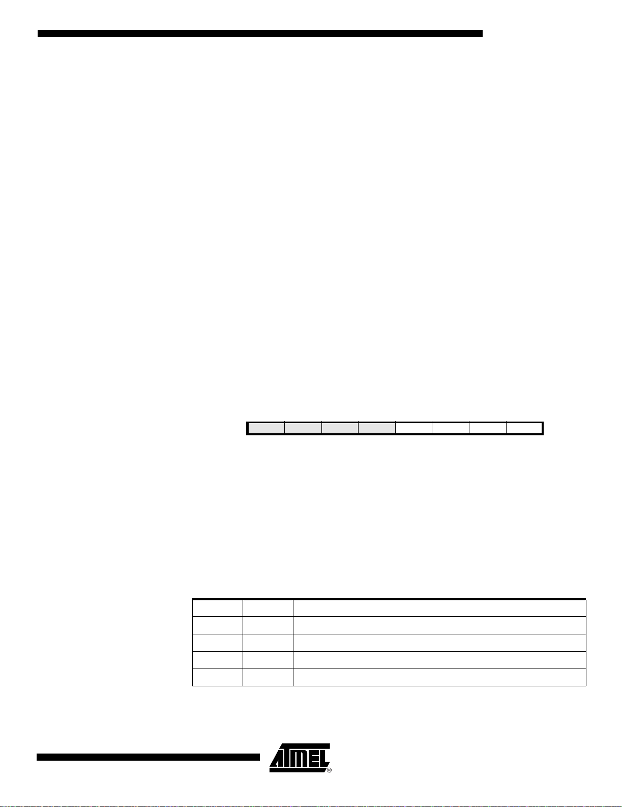
ATtiny2313
External Interrupts The External Interrupts are triggered by the INT0 pin, INT1 pin or any of the PCINT15..0
pins. Observe that, if enabled, the interrupts will trigger even if the INT0, INT1or
PCINT15..0 pins are configured as outputs. This feature provides a way of generating a
software interrupt. The pin change interrupt PCI1 will trigger if any enabled PCINT15..8
pin toggles. Pin change interrupt s PCI0 will trigge r if any enabl ed PCINT7..0 pin toggl es.
The PCMSK1 a nd PC MSK0 Regi sters cont rol wh ich pins co ntribute to the pin chan ge
interrupts. Pin change interrupt s on PCINT15.. 0 are detected asynchronously. Th is
implies that these interrupts can be used for waking the part also from sleep modes
other than Idle mode.
The INT0 and INT1 interrupts can be triggered by a falling or rising edge or a low level.
This is set up as indicated in the specification for the External Interrupt Control Register
A – EICRA. When the INT0 or INT1 interrupt is enabled and is configured as level triggered, the interrupt will trigger as long as the pin is held low. Note that recognitio n of
falling or rising edge interrupts on INT0 and INT1 requires the presence of an I/O clock,
described in “Clock Systems an d their Di stribution” o n page 22. L ow level i nterrupt on
INT0 and INT1 is detected asynchronously. This implies that this interrupt can be used
for waking the part from sleep modes other than Idle mod e. The I/ O clock is halted in all
sleep modes except Idle mode.
Note that if a level triggered interrupt is used for wake-up from Power-down, the
required level must be held long enough for the MCU to complete the wake-up to tr igger
the level interrupt. If the level disappears before the end of the Start-up Time, the MCU
will still wake up, but no interrupt will be generated. The start-up tim e is defined by the
SUT and CKSEL Fuses as described in “System Clock and Clock Options” on page 22.
MCU Control Register – MCUCR
The External Interrupt Control Register A contains control bits for interrupt sense
control.
Bit 76543210
PUD SM1 SE SMD ISC11 ISC10 ISC01 ISC00 MCUCR
Read/Write R/W R/W R/W R/W R/W R/W R/W R/W
Initial Value00000000
• Bit 3, 2 – ISC11, ISC10: Interrupt Sense Control 1 Bit 1 and Bit 0
The External Interrupt 1 is activated by the external pin INT1 if the SREG I-flag and the
corresponding interrupt mask are set. The level and edges on the external INT1 pin that
activate the interrupt are defined in Table 33. The value on the INT1 pin is sampled
before detecting edges. If edge or toggle interrupt is selected, pulses that last longer
than one clock period will generate an interrupt. Shorter pu lses are not guaranteed to
generate an int errupt. If low lev el interrup t is sele cted, th e low lev el m ust be h eld unt il
the completion of the currently executing instruction to generate an i nter rupt.
Table 32. Interrupt 0 Sense Control
ISC11 ISC10 Description
0 0 The low level of INT1 generates an interrupt request.
0 1 Any logical change on INT1 generates an interrupt request.
1 0 The falling edge of INT1 generates an interrupt request.
1 1 The rising edge of INT1 generates an interrupt request.
2543A–AVR–08/03
61
Page 62

• Bit 1, 0 – ISC01, ISC00: Interrupt Sense Control 0 Bit 1 and Bit 0
The External Interrupt 0 is activated by the external pin INT0 if the SREG I-flag and the
corresponding interrupt mask are set. The level and edges on the external INT0 pin that
activate the interrupt are defined in Table 33. The value on the INT0 pin is sampled
before detecting edges. If edge or toggle interrupt is selected, pulses that last longer
than one clock period will generate an interrupt. Shorter pu lses are not guaranteed to
generate an int errupt. If low lev el interrup t is sele cted, th e low lev el m ust be h eld unt il
the completion of the currently executing instruction to generate an i nter rupt.
Table 33. Interrupt 0 Sense Control
ISC01 ISC00 Description
0 0 The low level of INT0 generates an interrupt request.
0 1 Any logical change on INT0 generates an interrupt request.
1 0 The falling edge of INT0 generates an interrupt request.
1 1 The rising edge of INT0 generates an interrupt request.
General Interrupt Mask Register – GIMSK
Bit 76543210
INT1 INT0 PCIE
Read/WriteR/WR/WRRRRRR/W
Initial Value00000000
– – – – –GIMSK
• Bit 7 – INT1: External Interrupt Request 1 Enable
When the INT1 bit is set (one) and the I-bit in the Status Register (SREG) is set (one),
the external pin interrupt is enabled. The Interrupt Se nse Control1 bi ts 1/0 (ISC11 and
ISC10) in the MCU Control Regist er – MCUCR – def ine whether the external inter rupt is
activated on rising and/or falling edge of the INT1 pin or level sensed. Activity on the pi n
will cause an interrupt request even if INT1 is configured as an output. The corresponding interrupt of External Interrupt Request 1 is executed from the INT1 Interrupt Vecto r.
• Bit 6 – INT0: External Interrupt Request 0 Enable
When the INT0 bit is set (one) and the I-bit in the Status Register (SREG) is set (one),
the external pin interrupt is enabled. The Interrupt Se nse Control0 bi ts 1/0 (ISC01 and
ISC00) in the MCU Control Regist er – MCUCR – def ine whether the external inter rupt is
activated on rising and/or falling edge of the INT0 pin or level sensed. Activity on the pi n
will cause an interrupt request even if INT0 is configured as an output. The corresponding interrupt of External Interrupt Request 0 is executed from the INT0 Interrupt Vecto r.
• Bit 5 – PCIE: Pin Change Interrupt Enable
62
When the PCIE bit is set (one) and the I-bit in the Status Register (SREG) is set (one),
pin change interrupt 1 is enabled. Any change on any enabled PCINT7..0 pin will cause
an interrupt. The corres ponding interrupt o f Pin Chan ge Interrupt R equest is executed
from the P CI Interrupt Vecto r. PCIN T7..0 pins a re e nabl ed indi vidual ly by t he PCMS K
Register.
ATtiny2313
2543A–AVR–08/03
Page 63

ATtiny2313
External Interrupt Flag Register – EIFR
Bit 76543210
INTF1 INTF0 PCIF
Read/WriteR/WR/WRRRRRR/W
Initial Value00000000
– – – – –EIFR
• Bit 7 – INTF1: External Interrupt Flag 1
When an edge or logic change on the INT1 pi n triggers an interrupt request, INTF1
becomes set (one). If the I-bit in SREG and the INT1 bit in GIMSK are set (one), the
MCU will jump to the corresponding Interrupt Vector. The flag is cleared when the interrupt routine is executed. Alternatively, the flag can be cleared by writing a logical one to
it. This flag is always cleared when INT1 is configured as a level interrupt.
• Bit 6 – INTF0: External Interrupt Flag 0
When an edge or logic change on the INT0 pi n triggers an interrupt request, INTF0
becomes set (one). If the I-bit in SREG and the INT0 bit in GIMSK are set (one), the
MCU will jump to the corresponding Interrupt Vector. The flag is cleared when the interrupt routine is executed. Alternatively, the flag can be cleared by writing a logical one to
it. This flag is always cleared when INT0 is configured as a level interrupt.
• Bit 5 – PCIF: Pin Change Interrupt Flag
When a logic change on any PCINT7..0 pin triggers an interrupt request, PCIF becomes
set (one). If the I-b it in SREG an d the PCIE bit in G IMSK are se t (one), the MCU will
jump to the correspo nding Int errupt Vector . The fl ag is cl eared when the int errupt rou tine
is executed. Alternati vely, the flag can be cleared by writing a logical one to it.
Pin Change Mask Register – PCMSK
Bit 76543210
PCINT7 PCINT6 PCINT5 PCINT4 PCINT3 PCINT2 PCINT1 PCINT0 PCMSK
Read/Write R/W R/W R/W R/W R/W R/W R/W R/W
Initial Value00000000
• Bit 7..0 – PCINT7..0: Pin Change Enable Mask 15..8
Each PCINT7..0-bit selects whether pin change interrupt is enabled on the corresponding I/O pin. If PCINT7..0 is set and the PCIE bit in GIMSK is set, pin change interrupt is
enabled on the corresp onding I/O pin. If PC INT7..0 is cleared, pi n change interrupt on
the corresponding I/O pin is disabled.
2543A–AVR–08/03
63
Page 64

8-bit Timer/Cou nter0 with PWM
Timer/Counter0 is a general purpose 8-bit Timer/Counter module, with two independent
Output Compare Units, and with PWM support. It allows accurate program execution
timing (event management) and wave generat ion. The main fea tur es are:
•
Two Independent Output Compare Units
• Double Buffered Output Compare Registers
• Clear Timer on Compare Match (Auto Reload)
• Glitch Free, Phase Correct Pulse Width Modulator (PWM)
• Variable PWM Period
• Frequency Generator
• Three Independent Interrupt Sources (TOV0, OCF0A, and OCF0B)
Overview A simplified block diagram of the 8-bit Timer/Counter is shown in Figure 26. For the
actual placement of I/O pins, refer to “Pinout ATtiny 2313” on page 1 . CPU acces sible
I/O Registers, including I/O bits and I/O pins, are shown in bold. The device-specific I/O
Register and bit locations are listed in the “8-bit Timer/Counter Register Description” on
page 75.
Figure 26. 8-bit Timer/Counter Block Diagram
Timer/Counter
TCNTn
=
Count
Clear
Direction
Control Logic
TOP BOTTOM
=
clk
Tn
=
0
TOVn
(Int.Req.)
Clock Select
Edge
Detector
( From Prescaler )
OCnA
(Int.Req.)
Waveform
Generation
Tn
OCnA
OCRnA
=
DATA BUS
OCRnB
TCCRnA TCCRnB
Fixed
TOP
Value
OCnB
(Int.Req.)
Waveform
Generation
OCnB
Registers The Timer/Counter (TCNT0) and Output Compare Registers (OCR0A and OCR0B) are
8-bit registers. I nterrupt request (abbreviated to Int.Req. in the figure) signals are all visible in the Timer Interrupt Flag Register (TIFR). All interrupts are individually masked
with the Timer Interrupt Mask Register (TIMSK). TIFR and TIMSK are not shown in the
figure.
The Timer/Counter can be clocked internally, via the prescaler, or by an external clock
source on the T0 pin. The Cloc k Select logic block c ontrol s which cl ock sou rce and edge
the Timer/Counter uses to increment (or decrement) its value. The Timer/Counter is
inactive when no clock source is selected. The output from the Clock Select logic is
referred to as the timer clock (clk
T0
).
The double buffered Output Compare Registe rs (OCR0A and OCR0B) is compar ed with
the Timer/Counter value at all times. T he result of the compare can be used by the
Waveform Generator to generate a PWM or variable frequency output on the Output
64
ATtiny2313
2543A–AVR–08/03
Page 65

ATtiny2313
Compare pins (OC0A and OC0B ). See “Output Com pare Unit” on page 66. for d etails.
The Compare Match event will also set the Compare Flag (OC F0A or OCF0B) whic h
can be used to generate an Output Compare inter rupt request.
Definitions Many register and bi t r eferences in this section are written in general form. A lower case
“n” replaces the Tim er/Co unter num ber, in t his case 0 . A lower ca se “x” re places the
Output Compare Unit, in this case Compare Unit A or Compare Unit B. However, when
using the register or bit defines in a program, the precise form must be used, i.e.,
TCNT0 for accessing Timer/Counter0 counter value and so on.
The definitions in Table 34 are also used extensively throughout the document.
Table 34. Definitions
BOTTOM The counter reaches the BOTTOM when it becomes 0x00.
MAX The counter reaches its MAXimum when it be comes 0xF F (dec imal 255) .
TOP The counter reaches the TOP when it becomes equal to the highest
value in the count sequence. The TOP value can be assigned to be the
fixed value 0xFF (MAX) or the value stored in the OCR0A Register. The
assignment is dependent on the mode of operation.
Timer/Counter Clock Sources
The Timer/Counter can be clocked by an internal or an external clock source. The clock
source is selected by the Clock Select logic which is controlled by the Clock S elect
(CS02:0) bits located in the Timer/Counter Con trol Register (TCCR0B ). For details on
clock sources and prescaler, see “Timer/Counter0 and Timer/Co unter1 Pres calers” on
page 81.
Counter Unit The main part of the 8-bit Timer/ Counter is the programmabl e bi-di rectional counter uni t.
Figure 27 shows a block diagram of the counter and its surro undings.
Figure 27. Counter Unit Block Diagram
TOVn
top
(Int.Req.)
clk
Tn
Clock Select
Edge
Detector
( From Prescaler )
Tn
DATA BUS
count
TCNTn Control Logic
clear
direction
bottom
Signal description (i nternal signals):
count Increment or decrement TCNT0 by 1.
2543A–AVR–08/03
direction Select between increment and decrement.
clear Clear TCNT0 (set all bits to zero).
clk
Tn
Timer/Counter clock, referred to as clkT0 in the following.
top Signalize that TCNT0 has reached maximum value.
bottom Signalize that TCNT0 has reached minimum value (zero).
65
Page 66

Depending of the mode of operation used, the counter is cleared, incremented, or decremented at each timer clock (clk
). clkT0 can be generated from an external or internal
T0
clock source, se lected by the Clock Select bi ts (CS02:0). When no clock s ource is
selected (CS02:0 = 0) t he timer is stopped. However, t he TCNT0 valu e can be accessed
by the CPU, regardless of whether clk
is present or n ot. A CP U write overri des (has
T0
priority over) all counter clear or count operations.
The counting sequence is determined by the setting of the WGM01 and WGM00 bits
located in the Timer/Counter Control Register (TCCR0A) and the WGM02 bit located in
the Timer/Counter Control Register B (TCCR0B). There are close connections between
how the counter behaves (counts) and how waveforms are generated on the Output
Compare output OC0 A. For more details about ad vanced counting sequ ences and
waveform generation, see “Modes of Operation” on page 95.
The Timer/Counter Overflow Flag (TOV0) is set according to the mode of operation
selected by the WGM01:0 bits. TOV0 can be used for generating a CPU interrupt.
Output Compare Unit The 8-bit compa rator co ntinuousl y com pares TC NT0 with th e Out put C ompare Regi s-
ters (OCR0A and OCR0B). Whenever TCNT0 equals OCR0A or OCR0B, the
comparator signals a match. A m atch will s et the Outpu t Compar e Flag (OCF0A or
OCF0B) at the next timer clock cycle. If the corresponding interrupt is enabled, the Output Compare Flag gener ates an Output Compare i nterrupt. The Output Compare Flag is
automatical ly cleared when the interrupt is executed. Alternatively, the flag can be
cleared by software by writing a logical one to its I/O bit location. The Waveform Generator uses the match signal to gener ate an output accor ding to oper ating mode set by the
WGM02:0 bits and Compa re O utput mode (CO M0x1:0) bit s. The m ax and bottom signals are used by the Waveform Generator for handling the special cases of the extreme
values in some modes of operation (see “Modes of Operation” on page 95).
Figure 28 shows a block diagram of the Output Compare unit.
Figure 28. Output Compare Unit, Block Diagram
DATA BUS
OCRnx
= (8-bit Comparator )
top
bottom
FOCn
Waveform Generator
WGMn1:0
COMnX1:0
TCNTn
OCFnx (Int.Req.)
OCnx
66
ATtiny2313
2543A–AVR–08/03
Page 67

ATtiny2313
The OCR0x Registers are double buffered when using any of the Pulse Width Modulation (PWM) modes. For the normal and Clear Timer on Compare (CTC) modes of
operation, the double buffering is disabled. The double buffering synchronizes the
update of the OCR0x Co mpare Registers to either top or bottom of the counting
sequence. The synchronizat ion prevent s the occurre nce of odd-leng th, non-sy mmetrical
PWM pulses, thereby making the output glitch-free.
The OCR0x Register access may seem complex, but this is not case. When the double
buffering is enabled, the CPU has access to t he OCR0x Buf fer Register, and if double
buffering is disabled the CPU will access the OCR0x directly.
Force Output Compare In non-PWM waveform generat ion mo des, th e match output of the comparato r can be
forced by writing a one to the Force Output Compare (FOC0x) bit. Forcing Compare
Match will not se t the OCF0 x Flag or rel oad/clear t he timer, but the OC0 x pin will be
updated as if a real Compare M atch had occu rred (the COM0x1: 0 bits settings defi ne
whether the OC0x pin is set, cleared or toggled).
Compare Match Blocking by TCNT0 Write
Using the Output Compare Unit
All CPU write operations to the TCNT0 Register will block any Co mpare Match that
occur in the next timer clock cycle, even when the timer is stopped. This feature allows
OCR0x to be initialized to t he same value a s TCNT0 without triggeri ng an interrupt when
the Timer/Counter clock is enabled.
Since writing TCNT0 in any mode of operation will block all Compare Matches for one
timer clock cycle, there are ri sks invol ved when changing TCNT0 when using the Outpu t
Compare Unit, indepen dently of whether t he Timer/Count er is running or not. If the
value written to TCNT0 equals the OCR0x value, the Compare Match will be missed,
resulting in incorrect waveform generation. Similarly, do not write the TCNT0 value
equal to BOTTOM when the counter is down-counting.
The setup of the OC0x should be performed before setting the Data Direction Register
for the port pin to output. The easiest way of setting the OC0x value is to use the Force
Output Compare (FOC0x) strobe b its in Normal mode . The O C0x Registers keep their
values even when changing between Waveform Generation modes.
Be awar e that the CO M0x1 :0 bits are n ot dou ble bu ffer ed toge ther with t he co mpare
value. Changing the COM0x1:0 bits will take effect immediately.
2543A–AVR–08/03
67
Page 68
Compare Match Output Unit
The Compare Output mode (COM0x1:0) bits ha ve two functions. The Waveform Generator uses the COM0x1:0 bits for defining the Output Compare (OC0x) state at the next
Compare Match. Also, the COM0x1:0 bits c ontrol the OC0x pin output source. Figure 29
shows a simplified schematic of the logic affected by the COM0x1:0 bit setting. The I/O
Registers, I/O bits, and I/O pins in the figure are shown in bold. Only the parts of the
general I/O Port Control Registers (DDR and PORT) that are affected by t he COM0x1:0
bits are shown. When referring to the OC0x state, the reference is for the internal OC0x
Register, not the OC0x pin. If a system reset occur, the OC0x Register is reset to “0”.
Figure 29. Compare Match Output Unit, Schematic
COMnx1
COMnx0
FOCn
clk
I/O
Waveform
Generator
DQ
1
OCnx
DQ
PORT
DATA BUS
DQ
DDR
0
OCn
Pin
The general I/O port function is overridden by the Output Compare (OC0x) from the
Waveform Generator if either of the COM0x1:0 bits are set. However, the OC0x pin
direction (input or output) is still controlled by the Data Direction Register (DDR) for the
port pin. The Data Direction Register bit for the OC0x pin (DDR_OC0x) must be set as
output before the OC0x value is visible on the pin. The port o verride function is i ndependent of the Waveform Generation mode.
The design of the Output Compare pin logic all ows initial izat ion of the OC0x stat e before
the output is enabled. Note th at some COM 0x1:0 bit settings ar e reserved for certa in
modes of operation. See “8-bit Timer/Counter Register Descriptio n” on page 75.
Compare Output Mode and Waveform Generation
68
ATtiny2313
The Waveform Generator uses th e COM0x1:0 bit s diff erentl y in Normal , CTC, and PWM
modes. For all modes, setting the COM0x1:0 = 0 tells the Waveform Generator that no
action on the OC0x Register is to be performed on the next Compare Match. For compare output actions in the non-PW M modes refer to Figur e 28 on pa ge 66. For f ast PWM
mode, refer to Table 27 on page 56, and for phase correct PWM refe r to Table 28 on
page 57.
A change of the COM0x1:0 bits state will have effect at the first Compare Match after
the bits are written. For non-PW M modes , the action can be forced to have immed iate
effect by using the FOC0x strobe bits.
2543A–AVR–08/03
Page 69
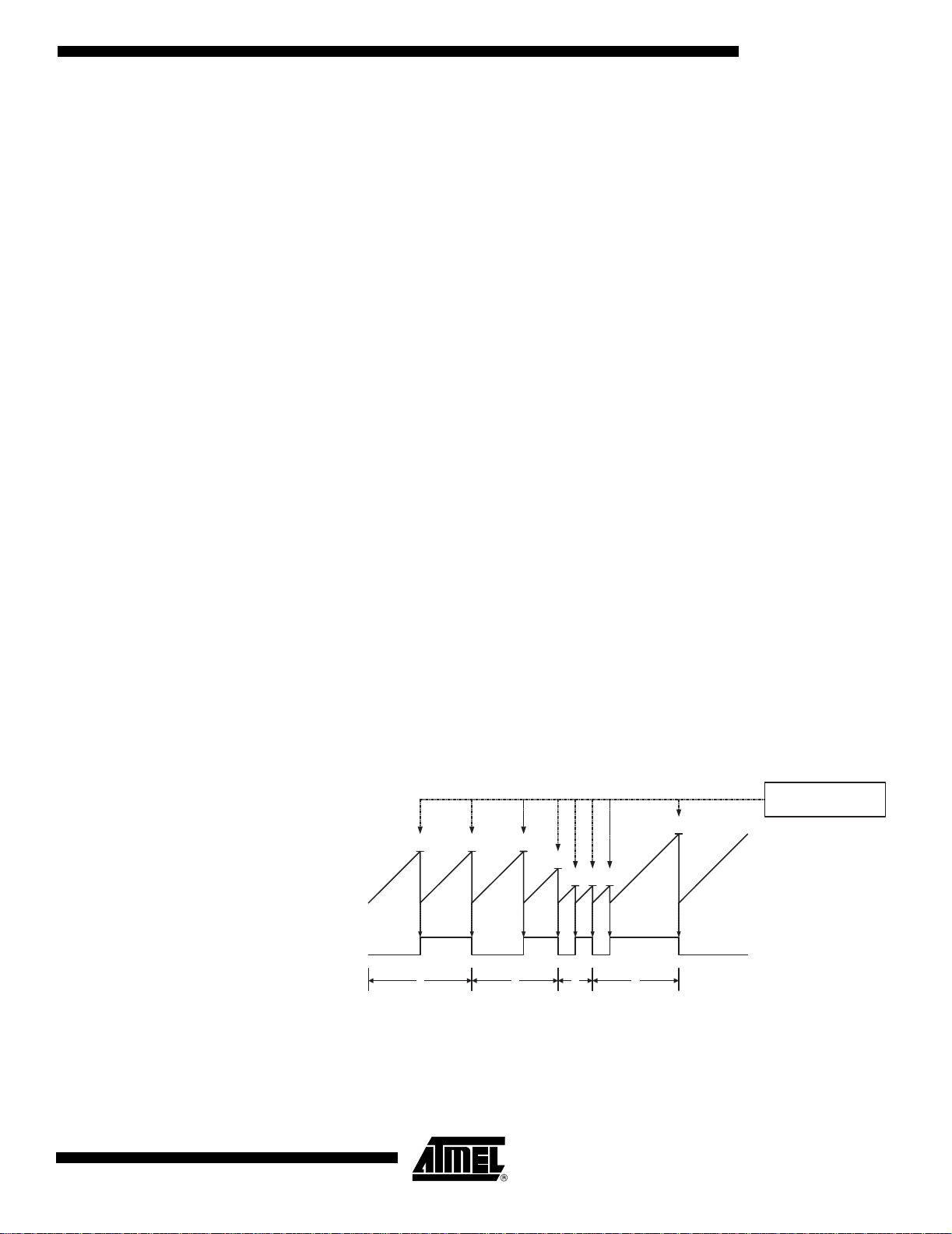
ATtiny2313
Modes of Operation The mode of operation, i .e. , t he behavior of the Timer/Counter and the Output Compare
pins, is defined by the combination of the Waveform Generation mode (WGM02:0) and
Compare Output mode (COM0x1:0) bits. The C ompare Output mode bits do not affect
the counting sequence, w hile the W aveform Ge neration m ode bits d o. The CO M0x1:0
bits control whe ther the PWM output gene rated sho uld be invert ed or not (inver ted or
non-inverted PWM). For non-PWM modes the COM0x1:0 b its control wh ether the output should be set, cleared, or toggled at a Compare Match (See “Compare Match
Output Unit” on page 68.).
For detailed timing information refer to Figure 33, Figure 34, Figure 35 and Figure 36 in
“Timer/Counter Timing Diagrams” on page 73.
Normal Mode The simplest mo de of operation is the Normal mode (WGM 02:0 = 0). In this mod e the
counting direction is always up (incrementing), and no counter clear is performed. The
counter simply overruns when it passes its maximum 8-bit value (TOP = 0xFF) and then
restarts from the bottom (0x00 ). In normal operation the Time r/Counter Overflow F lag
(TOV0) will be set in the same timer clock cycle as the TCNT0 bec omes zero. The
TOV0 Flag in this case beh aves like a nin th bit, excep t that it is onl y set, not cleared.
However, combined with the timer overflow interrupt that automatically clears the TOV0
Flag, the timer resolution can be increased by so ftware. There are no special cases to
consider in the Normal mode, a new counter value can be written anytime.
Clear Timer on Compare Match (CTC) Mode
The Output Compare Unit can be used to generate interrupts at some given time. Using
the Output Compare t o generate wavefo rms in Normal mode is not recom mended,
since this will occupy too much of the CPU time.
In Clear Timer on Compare or CTC mode (WGM02:0 = 2), the OCR0A Register is used
to manipulate the counter resolution. In CTC mode the counter is cleared to zero when
the counter value (TCNT0) matches the OCR0A. The OCR0A defines the top value for
the counter, hence also its resolution. This mode allows greater control of the Compare
Match output frequency. It also simplifies the operation of counting external events.
The timing diagram for the CTC mode is shown in Figure 3 0. The counter value
(TCNT0) increases until a Compare Match occurs between TCNT0 and OCR0A, and
then counter (TCNT0) is cleared.
Figure 30. CTC Mode, Timing Diagram
OCnx Interrupt Flag Set
TCNTn
OCn
(Toggle)
Period
1 4
2 3
(COMnx1:0 = 1)
2543A–AVR–08/03
An interrupt can be gene rated each time the co unte r val ue reac hes t he T OP va lue by
using the OC F0A F lag. If the inte rrupt is enabl ed, t he in terrupt handl er routin e c an be
used for updating the TOP value. However, changing TOP to a value close to BOTTOM
when the counter is running with none or a low prescaler value must be done with care
since the CTC mode does not have the double buffering feature. If the new value written
69
Page 70

to OCR0A is lower than the current value of TCNT0, the counter will miss the Compare
Match. The co unter will then h ave to count to its maximum value (0xFF) an d wrap
around starting at 0x00 before the Compare Match can occur.
For generating a waveform output in CTC mode, the OC0A output can be set to toggle
its logical level on each Compar e Matc h by sett ing th e Compar e Out put mod e bits to
toggle mode (COM0A1:0 = 1). The OC0A value will not be visible on the port pin unless
the data direction for the pin is set to output. The waveform generated will have a maximum frequency of f
OC0
= f
/2 when OCR0A is set to zero (0x00). The waveform
clk_I/O
frequency is defined by the following equation:
f
f
OCnx
------------------------------------------------- -=
2 N 1 OCRnx+()⋅⋅
clk_I/O
The N variable represents the prescale factor (1, 8, 64, 256, or 1024) .
As for the Normal mode o f operation, the TOV0 Flag is set in the same timer clock cycle
that the counter counts from MAX to 0x00.
Fast PWM Mode The fast Pulse Width Modu lati on or fas t PWM mode (WGM02 :0 = 3 or 7) prov ides a hi gh
frequency PWM waveform generation option. The fast PWM differs from the other PWM
option by its single-slope operation. The counter counts from BOTTOM to TOP then
restarts from BOTTOM. TOP is defined as 0xFF when WGM2:0 = 3, and OCR0A when
WGM2:0 = 7. In non-inve rting Com pare Output mo de, the Output Compare (OC0 x) is
cleared on the C ompare Match betwe en TCN T0 and OC R0x, an d set at B OTTO M. I n
inverting Compare Output mode, the output is set on Compare Match and cleared at
BOTTOM. Due to the single-slope operat ion, the ope rating freque ncy of the fast PWM
mode can be twice as high as the phase correct PWM mode that use dual-slope operation. This high fr equency makes the fast PWM mod e well suit ed for power reg ulation,
rectification, and DAC applications. High frequency allows physically small sized external components (coils, capaci tors), and therefore reduces tot al system cost.
In fast PWM mode, the counter is incremented until the counter value matches the TOP
value. The counter is then clear ed at t he fol lowing timer clock cycle. The timing diagram
for the fast PWM mode is shown in Figure 29. The TCNT0 value is in t he timing diagram
shown as a histogram for illustrating the single-slope operation. The diagram includes
non-inverted and inverted PWM outputs. The small horizontal line marks on the TCNT0
slopes represent Compare Matches between OCR0x and TCNT0.
70
ATtiny2313
2543A–AVR–08/03
Page 71
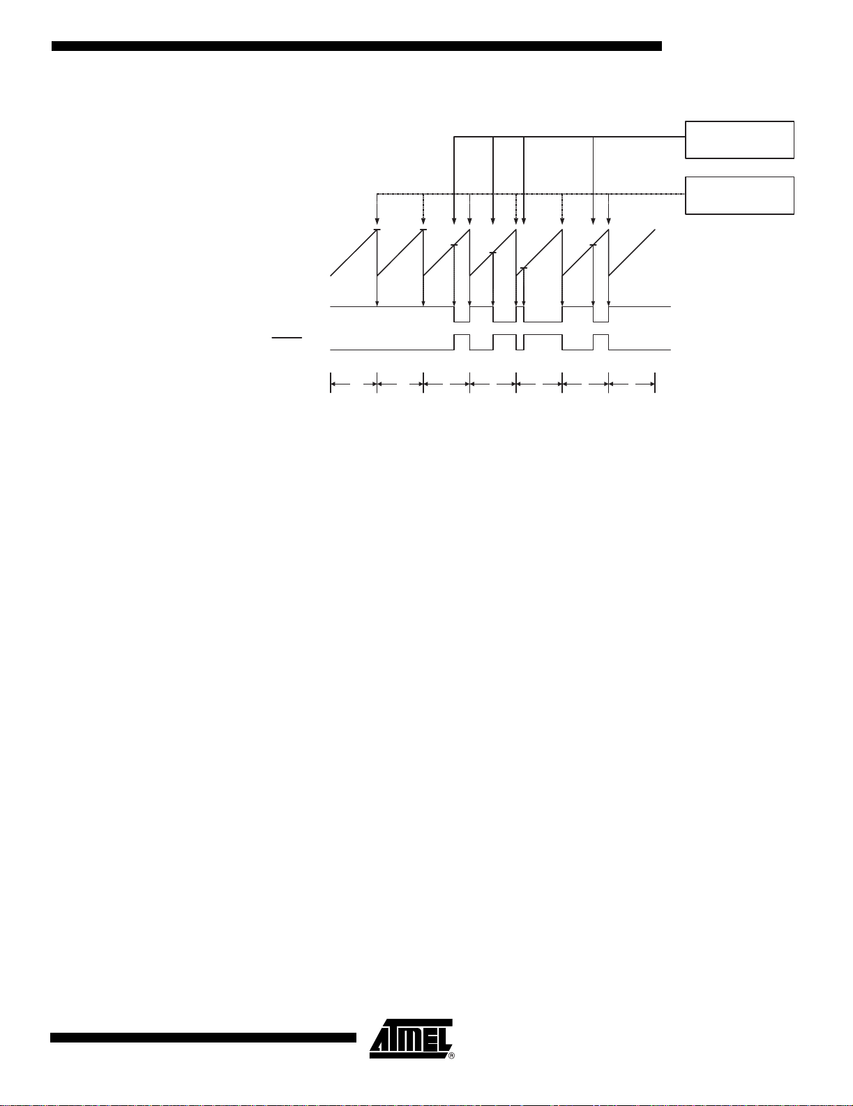
Figure 31. Fast PWM Mode, Timing Diagram
TCNTn
ATtiny2313
OCRnx Interrupt Flag Set
OCRnx Update and
TOVn Interrupt Flag Set
OCn
OCn
Period
1
2 3
4 5 6 7
(COMnx1:0 = 2)
(COMnx1:0 = 3)
The Timer/Counter Overflow Flag (TOV0) is set each time the counter reaches TOP. If
the interrupt is enabled, the interrupt handler routine can be used for updating the compare value.
In fast PWM mode , the compare unit allows genera tion of PWM wavef orms on the
OC0x pins. Setting the COM0x1:0 bits to two will produce a non-inverted PWM and an
inverted PWM output can be gen erate d by se ttin g the C OM0 x1:0 to three: Sett ing the
COM0A1:0 bits to one allowes the AC0A pin to toggle on Compare Matches if the
WGM02 bit is set. This option is not available for the OC0B pin (See Table 27 on page
56). The actual OC0x v alue will only be visible on the port pin if the data direction for the
port pin is s et as o utput. T he PWM w aveform is ge nera ted by setting (or cl earing) the
OC0x Register at the Compare Match between OCR0x and TCNT0, and clearing (or
setting) the OC0x Register at the timer clock cycle the counter is cleared (changes from
TOP to BOTTOM).
The PWM frequency for the output can be calculated by the following equation:
f
f
OCnxPWM
clk_I/O
------------------=
N 256⋅
2543A–AVR–08/03
The N variable represents the prescale factor (1, 8, 64, 256, or 1024) .
The extreme values for the OCR0A Register represents special cases when generating
a PWM waveform output in the fast PWM mode. If the OCR0A is set equal to BOTTOM,
the output will be a narrow spike for each MAX+1 timer clock cycle. Setting the OCR0A
equal to MAX will result in a constantly high or low output (depending on the polarity of
the output set by the COM0A1:0 bits.)
A frequency (with 50% duty cycle) wavef orm output in fast PWM mode can be achieved
by setting OC0x to toggl e its logical level on each Compare Match (COM0x1:0 = 1). The
waveform generated will have a maximum frequency of f
OC0
= f
/2 when OCR0A is
clk_I/O
set to zero. This feature is similar to the OC0A toggle in CTC mode, except the double
buffer feature of the Output Compare unit is enabled in the fast PWM mode.
71
Page 72
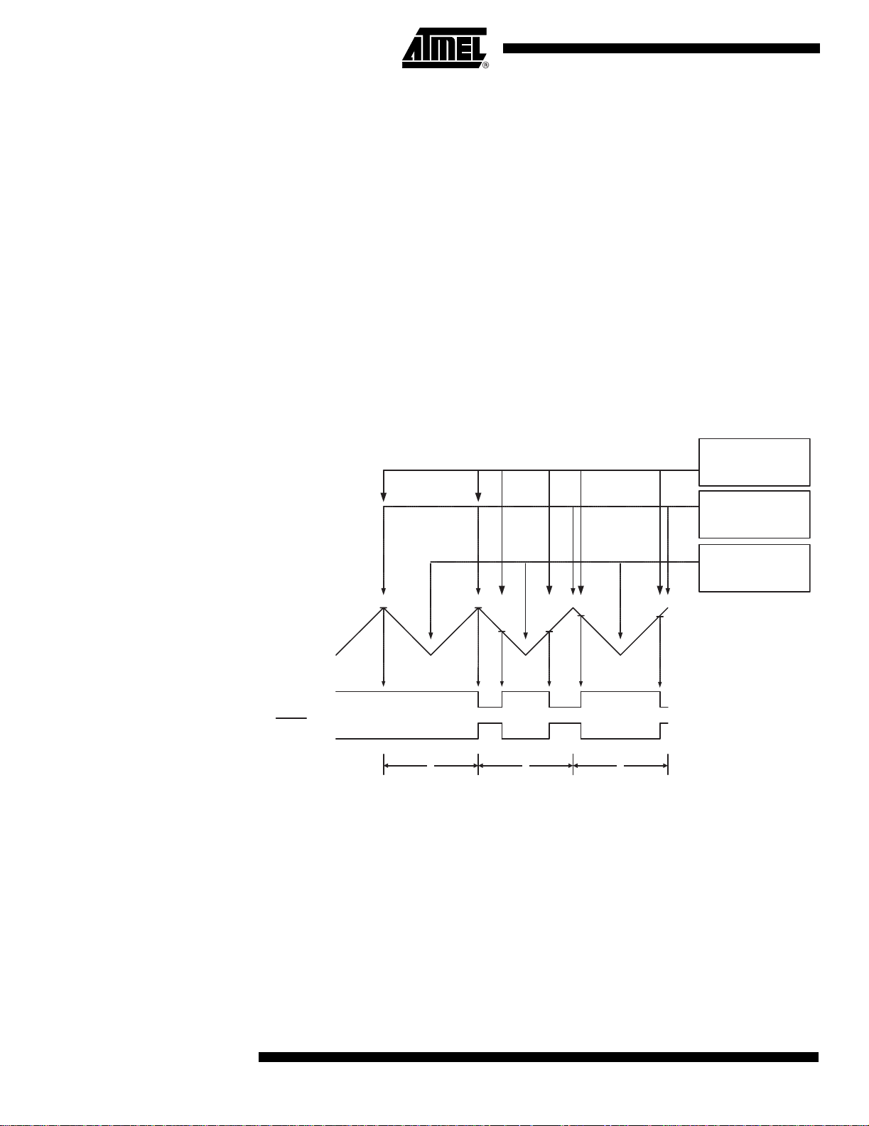
Phase Correct PWM Mode The phase correct PWM mode (WGM02:0 = 1 or 5) provides a high resolution phase
correct PWM waveform generation option. The phase correct PWM mode is based on a
dual-slope op eration. The coun ter count s repeated ly from BO TTOM to TOP and th en
from TOP to BOTTOM. TOP is defined as 0xFF when WGM2:0 = 1, and OCR0A when
WGM2:0 = 5. In non-inve rting Com pare Output mo de, the Output Compare (OC0 x) is
cleared on the Compare Match between TCNT0 and OCR0x while upcounting, and set
on the Compare Match while down-counting. In inverting Output Compare mode, the
operation is inverted. The dual-sl ope operation has l ower maximum operati on frequen cy
than single slope operation. However, due to the symmetric feature of the dual-slope
PWM modes, these modes are preferred for motor control applications.
In phase correct PWM mode th e counter is incremented u nti l the counter value matches
TOP. When the counter reaches TOP, it changes the count direction. The TCNT0 value
will be equal to TOP for one timer clock cycle. The timing diagram for the phase correct
PWM mode is shown on Figure 32. The TCNT0 value is in the timing di agram shown as
a histogram for illustrating the dual-slope operation. The diagram includes non-inverted
and inverted PWM outputs. The sma ll horizontal line marks on the TCNT0 slopes represent Compare Matches between OCR0x and TCNT0.
Figure 32. Phase Correct PWM Mode, Timing Diagram
OCnx Interrupt Flag Set
OCRnx Update
TOVn Interrupt Flag Set
TCNTn
OCn
OCn
Period
1 2 3
(COMnx1:0 = 2)
(COMnx1:0 = 3)
The Timer/Counter Overflow Flag (TOV0) is set each time the counter reaches BOTTOM. The Interrupt Flag can be used to generate an interrupt each time the counter
reaches the BOTTOM value.
In phase correct PWM mode, the compar e uni t allows g enera tion of PWM waveforms on
the OC0x pins. Setting the COM0x1:0 bits to two will produce a non-inverted PWM. An
inverted PWM output can be gen erate d by se ttin g the C OM0 x1:0 to three: Sett ing the
COM0A0 bits to one allows the OC0A pin to toggle on Compare Matches if the WGM02
bit is set. This option is not available for the OC0B pin (See Table 28 on page 57). The
actual OC0x value will only be visible on the port pin if the data direction for the port pin
is set as output. The PWM waveform is generated by clearing (or setting) the OC0x
Register at the Com pare M atch b etw een O CR0x and TC NT0 when the counte r inc rements, and setting (or clearing) the OC0x Register at Compare Match between OCR0x
72
ATtiny2313
2543A–AVR–08/03
Page 73

ATtiny2313
and TCNT0 when the counter decrements. The PWM frequency for the output when
using phase correct PWM can be calculated by the following equation:
f
clk_I/O
f
OCnxPCPWM
The N variable represents the prescale factor (1, 8, 64, 256, or 1024).
The extreme values for the OCR0A Register represent special case s when generating a
PWM waveform outpu t in the phase correct PWM mode. If the OCR 0A is set equal to
BOTTOM, the output will be continuously low and if set equal to MAX the output will be
continuously high for non-inverted PW M mo de. For inverted PWM the output w ill have
the opposite logic values.
At the very start of period 2 in Figure 32 OCn has a transition from high to low even
though there is no Compare Match. The point of this transition is to guaratee symmetry
around BOTTOM. There are two cases that give a transition wit hout Compare Match.
• OCR0A changes its value from MAX, like in Figure 32. When the OCR0A value is
MAX the OCn pin value is the same as the result of a down-counting Compare
Match. To ensure symmetry around BOTTOM the OCn value at MAX must
correspond to the result of an up-counti ng Compa re Match.
• The timer starts counting from a value highe r than the one in OCR0A, and for that
reason misses the Compare Match and hence the OCn change that would have
happened on the way up.
------------------=
N 510⋅
Timer/Counter Timing Diagrams
The Timer/Counter is a synchronou s design and the timer clock (clkT0) is therefore
shown as a clock enable signal in the following figures. The figures include information
on when Interrupt Flags are set. Figure 33 contains timing data for basic Timer/Counter
operation. T he figure s hows the co unt s equen ce close to the MA X va lue in all modes
other than phase correct PWM mode.
Figure 33. Timer/Counter Timing Diagram, no Prescaling
clk
I/O
clk
Tn
(clk
/1)
I/O
TCNTn MAX - 1 MAX BOTTOM BOTTOM + 1
TOVn
Figure 33 shows the same timing data, but with the prescaler enabled.
2543A–AVR–08/03
73
Page 74

Figure 34. Timer/Counter Timing Diag ram, wi th Prescaler (f
clk
I/O
clk
Tn
(clk
/8)
I/O
clk_I/O
/8)
TCNTn
TOVn
MAX - 1 MAX BOTTOM BOTTOM + 1
Figure 35 shows the setting of OCF0B in all modes and OCF0A in all modes except
CTC mode and PWM mode, where OCR0A is TOP.
Figure 35. Timer/Counter Timing Diagram, Set ti ng of OCF0x, with Prescal er (f
clk
I/O
clk
Tn
(clk
/8)
I/O
TCNTn
OCRnx
OCFnx
OCRnx - 1 OCRnx OCRnx + 1 OCRnx + 2
OCRnx Value
clk_I/O
/8)
Figure 36 shows the setting of OCF0A and the clearing of TCNT0 in CTC mode and fast
PWM mode where OCR0A is TOP.
74
ATtiny2313
Figure 36. Timer/Counter Timing Diagram, Clear Timer on Compare Match mode, with
Prescale r (f
clk
I/O
clk
Tn
(clk
/8)
I/O
TCNTn
(CTC)
OCRnx
OCFnx
clk_I/O
/8)
TOP - 1 TOP BOTTOM BOTTOM + 1
TOP
2543A–AVR–08/03
Page 75

8-bit Timer/Counter Register Description
ATtiny2313
Timer/Counter Control Register A – TCCR0A
Bit 76543210
COM0A1 COM0A0 COM0B1 COM0B0 – – WGM01 WGM00 TCCR0A
Read/Write R/W R/W R/W R/W R R R/W R/W
Initial Value 0 0 0 0 0 0 0 0
• Bits 7:6 – COM0A1:0: Compare Match Output A Mode
These bits control the Output Compare pin (OC0A) behavior. If one or both of the
COM0A1:0 bits are set, the O C0A ou tput overrides the normal port functionality of the
I/O pin it is connected to. However, note that the Data Direction Register (DDR) bit corresponding to the OC0A pin must be set in order to enable the output driver.
When OC0A is connected to the pin, the function of the COM0A1:0 bits depends on the
WGM02:0 bit setting. Table 35 shows the COM0A1:0 bit functionality when the
WGM02:0 bits are set to a normal or CTC mode (non-PWM).
Table 35. Compare Output Mode, non-PWM Mode
COM0A1 COM0A0 Description
0 0 Normal port operation, OC0A disconnected.
0 1 Toggle OC0A on Compare Match
1 0 Clear OC0A on Compare Match
1 1 Set OC0A on Compare Match
Table 36 shows the COM0A1:0 bit functionality when the WGM01:0 bits are set to fast
PWM mode.
Table 36. Compare Output Mode, Fast PWM Mode
COM0A1 COM0A0 Description
0 0 Normal port operation, OC0A disconnected.
0 1 WGM02 = 0: Normal Port Operation, OC0A Disconnected.
WGM02 = 1: Toggle OC0A on Compare Match.
1 0 Clear OC0A on Compare Match, set OC0A at TOP
1 1 Set OC0A on Compare Match, clear OC0A at TOP
Note: 1. A special case occurs when OCR0A equals TOP and COM0A1 is set. In this case,
the Compare Match is ignored, but the set or clear is done at TOP. See “Fast PWM
Mode” on page 70 for more details.
(1)
2543A–AVR–08/03
75
Page 76

Table 37 show s the COM0A1: 0 bit func tionality w hen th e WGM02:0 bits ar e set to
phase correct PWM mode.
Table 37. Compare Output Mode, Phase Correct PWM Mode
COM0A1 COM0A0 Description
0 0 Normal port operation, OC0A disconnected.
0 1 WGM02 = 0: Normal Port Operation, OC0A Disconnected.
WGM02 = 1: Toggle OC0A on Compare Match.
1 0 Clear OC0A on Compare Match when up-counting. Set OC0A on
Compare Match when down-countin g.
1 1 Set OC0A on Compare Match when up-counting. Clear OC0A on
Compare Match when down-countin g.
Note: 1. A special case occurs when OCR0A equals TOP and COM0A1 is set. In this case,
the Compare Match is ignored, but the set or clear is done at TOP. See “Phase Correct PWM Mode” on page 72 for more details.
(1)
• Bits 5:4 – COM0B1:0: Compare Match Output B Mode
These bits control the Output Compare pin (OC0B) behavior. If one or both of the
COM0B1:0 bits are set, the O C0B ou tput overrides the normal port functionality of the
I/O pin it is connected to. However, note that the Data Direction Register (DDR) bit corresponding to the OC0B pin must be set in order to enable the output driver.
When OC0B is connected to the pin, the function of the COM0B1:0 bits depends on the
WGM02:0 bit setting. Table 38 shows the COM0A1:0 bit functionality when the
WGM02:0 bits are set to a normal or CTC mode (non-PWM).
Table 38. Compare Output Mode, non-PWM Mode
COM0B1 COM0B0 Description
0 0 Normal port operation, OC0B disconnected.
0 1 Toggle OC0B on Compare Match
1 0 Clear OC0B on Compare Match
1 1 Set OC0B on Compare Match
Table 39 shows the COM0B1:0 bit functionality when the WGM02:0 bits are set to fast
PWM mode.
Table 39. Compare Output Mode, Fast PWM Mode
COM0B1 COM0B0 Description
0 0 Normal port operation, OC0B disconnected.
01Reserved
1 0 Clear OC0B on Compare Match, set OC0B at TOP
1 1 Set OC0B on Compare Match, clear OC0B at TOP
Note: 1. A special case occurs when OCR0B equals TOP and COM0B1 is set. In this case,
the Compare Match is ignored, but the set or clear is done at TOP. See “Fast PWM
Mode” on page 70 for more details.
(1)
76
ATtiny2313
2543A–AVR–08/03
Page 77

ATtiny2313
Table 40 show s the COM0B1: 0 bit func tionality w hen th e WGM02:0 bits ar e set to
phase correct PWM mode.
Table 40. Compare Output Mode, Phase Correct PWM Mode
COM0B1 COM0B0 Description
0 0 Normal port operation, OC0B disconnected.
01Reserved
1 0 Clear OC0B on Compare Match when up-counting. Set OC0B on
Compare Match when down-countin g.
1 1 Set OC0B on Compare Match when up-counting. Clear OC0B on
Compare Match when down-countin g.
Note: 1. A special case occurs when OCR0B equals TOP and COM0B1 is set. In this case,
the Compare Match is ignored, but the set or clear is done at TOP. See “Phase Correct PWM Mode” on page 72 for more details.
(1)
• Bits 3, 2 – Res: Reserved Bits
These bits are reserved bits in t he ATtiny2313 and will always read as zero.
• Bits 1:0 – WGM01:0: Waveform Generati on Mode
Combined with the WGM02 bit found in the TCCR0B Register, these bits control the
counting seque nce of the co unter, the source for maxim um (TOP) cou nter value , and
what type of waveform generation to be used, see Table 41. Mo des of operation supported by the Timer/Counter unit are: Normal mode (counter), Clear Timer on Compare
Match (CTC) mode, and two types of Pulse Width Modulation (PWM) modes (see
“Modes of Operation” on page 95).
Table 41. Waveform Generation Mode Bit Description
Timer/Counter
Mode of
Mode WGM2 WGM1 WGM0
0 0 0 0 Normal 0xFF Immediate MAX
1 0 0 1 PWM, Phase
2 0 1 0 CTC OCRA Immediate MAX
3 0 1 1 Fast PWM 0xFF TOP MAX
4 1 0 0 Reserved – – –
5 1 0 1 PWM, Phase
6 1 1 0 Reserved – – –
7 1 1 1 Fast PWM OCRA TOP TO P
Notes: 1. MAX = 0xFF
2. BOTTOM = 0x00
Operation TOP
0xFF TOP BOTTOM
Correct
OCRA TOP BOTTOM
Correct
Update of
OCRx at
TOV Flag
(1)(2)
Set on
2543A–AVR–08/03
77
Page 78

Timer/Counter Control Register B – TCCR0B
Bit 76543210
FOC0A FOC0B – – WGM02 CS02 CS01 CS00 TCCR0B
Read/Write W W R R R R R/W R/W
Initial Value 0 0 0 0 0 0 0 0
• Bit 7 – FOC0A: Force Output Compare A
The FOC0A bit is only active when the WGM bits specify a non-PWM mode.
However, for ensuring compati bili ty wit h future dev ices, thi s bit must be set to zero when
TCCR0B is written when operating in PWM mode. When writing a logical one to the
FOC0A bit, an immedi ate Compare Match is force d on the W aveform Gen eration uni t.
The OC0A output i s changed acco rding to its C OM0A1:0 bi ts setting. No te that the
FOC0A bit is implemented as a strobe. Therefore it is the value present in the
COM0A1:0 bits that determines the effect of the forced compare.
A FOC0A strobe will not generate any interrupt, nor will it clear the timer in CTC mode
using OCR0A as TOP.
The FOC0A bit is always read as zero.
• Bit 6 – FOC0B: Force Output Compare B
The FOC0B bit is only active when the WGM bits specify a non-PWM mode.
However, for ensuring compati bili ty wit h future dev ices, thi s bit must be set to zero when
TCCR0B is written when operating in PWM mode. When writing a logical one to the
FOC0B bit, an immedi ate Compare Match is force d on the W aveform Gen eration uni t.
The OC0B output i s changed acco rding to its C OM0B1:0 bi ts setting. No te that the
FOC0B bit is implemented as a strobe. Therefore it is the value present in the
COM0B1:0 bits that determines the effect of the forced compare.
A FOC0B strobe will not generate any interrupt, nor will it clear the timer in CTC mode
using OCR0B as TOP.
The FOC0B bit is always read as zero.
• Bits 5:4 – Res: Reserved Bits
These bits are reserved bits in t he ATtiny2313 and will always read as zero.
• Bit 3 – WGM02: Waveform Generation Mode
See the description in the “Timer/Counter Control Register A – TCCR0A” on page 75.
• Bits 2:0 – CS02:0: Clock Select
The three Clock Select bits select the clock source to be used by the Timer/Counter.
Table 42. Clock Select Bit Description
CS02 CS01 CS00 Description
0 0 0 No clock source (Timer/Counter stopped)
001clk
010clk
011clk
100clk
/(No prescaling)
I/O
/8 (Fro m prescaler)
I/O
/64 (From prescaler)
I/O
/256 (From prescaler)
I/O
78
ATtiny2313
2543A–AVR–08/03
Page 79

Table 42. Clock Select Bit Description (Continued)
CS02 CS01 CS00 Description
ATtiny2313
Timer/Counter Register – TCNT0
Output Compare Register A – OCR0A
101clk
/1024 (From prescaler)
I/O
1 1 0 External clock source on T0 pin. Clock on falling edge.
1 1 1 External clock source on T0 pin. Clock on rising edge.
If external pin modes are used for the Timer/Counter0, transitions on the T0 pin will
clock the counter even if the pin is configured as an output. This feature allows software
control of the counting.
Bit 76543210
TCNT0[7:0] TCNT0
Read/Write R/W R/W R/W R/W R/W R/W R/W R/W
Initial Value00000000
The Timer/Counter Register gives direct access, both for read and write operations, to
the Timer/Counte r unit 8 -bit c ounter. Writin g to th e TC NT0 Register blo cks (rem oves)
the Compare Match on the followi ng timer clock. Modifying the counter (TC NT0) whi le
the counter is running, introduces a risk of missing a C ompare Match bet ween TCN T0
and the OCR0x Registers.
Bit 76543210
OCR0A[7:0] OCR0A
Read/Write R/W R/W R/W R/W R/W R/W R/W R/W
Initial Value00000000
Output Compare Register B – OCR0B
Timer/Counter Interrupt Mask Register – TIMSK
The Output Compare Register A contains an 8-bit value that is continuously compared
with the counter value (TCNT0). A match can be used to generate an Output Compare
interrupt, or to generate a waveform output on the OC0A pin.
Bit 76543210
OCR0B[7:0] OCR0B
Read/Write R/W R/W R/W R/W R/W R/W R/W R/W
Initial Value00000000
The Output Compare Register B contains an 8-bit value that is continuously compared
with the counter value (TCNT0). A match can be used to generate an Output Compare
interrupt, or to generate a waveform output on the OC0B pin.
Bit 76543210
TOIE1 OCIE1A OCIE1 B – ICIE1 OCIE0B TOIE0 OCIE0A TIMSK
Read/WriteRRRRR/WR/WR/WR
Initial Value00000000
• Bit 2 – OCIE0B: Timer/Counter0 Output Compare Match B Interrupt Enable
When the OCIE0B bit is written to one, and the I-bit in the Status Register is set, the
Timer/Counter Compare Match B interrupt is enabled. The corresponding interrupt is
executed if a Compare Match i n Timer/ Counter occ urs, i .e., when t he OCF0B bit i s set i n
the Timer/Counter Interrupt Flag Register – TIFR.
2543A–AVR–08/03
79
Page 80

• Bit 1 – TOIE0: Timer/Counter0 Overflow Interrupt Enable
When the TOIE0 bit is written to one, an d the I-bit in the Status R egister is set, the
Timer/Counter0 Overflow inter rupt is enabl ed. The corr espon ding interr upt is executed if
an overflow in Timer/Counter0 occurs, i.e., when the TOV0 bit is set in the
Timer/Counter 0 Interrupt Flag Register – TIFR.
• Bit 0 – OCIE0A: Timer/Counter0 Output Compare Match A Interrupt Enable
When the OCIE0A bit is written to one, and the I-bit in the Status Register is set, the
Timer/Counter0 Co mpare M atch A i nterrupt is e nabled . The correspo nding interrupt is
executed if a Compare Match in Timer/Counter0 occurs, i.e., when the OCF0A bit is set
in the Timer/Counter 0 Interr upt Flag Register – TIFR.
Timer/Counter Interrupt Flag Register – TIFR
Bit 76543210
TOV1 OCF 1A OCF1B – ICF 1 OCF0B TOV0 OCF0A TIFR
Read/Write R R R R R/W R/W R/W R
Initial Value00000000
• Bits 4, 0 – Res: Reserved Bits
These bits are reserved bits in t he ATtiny2313 and will always read as zero.
• Bit 2 – OCF0B: Output Compare Flag 0 B
The OCF0B bit is set wh en a C ompa re Match o ccurs be tween th e T imer/Cou nter and
the data in OCR0B – Output Compare R egister0 B. OCF0B is cleared by h ardware
when executing the corresponding interrupt handling vector. Alternatively, OCF0B is
cleared by writing a logic one to the flag. When the I-bit in SREG, OCIE0B
(Timer/Counte r Compare B Match Inte rrupt Enable), and OCF0B are set, the
Timer/Counter Compare Match Interrupt is executed.
• Bit 1 – TOV0: Timer/Counter0 Overflow Flag
The bit TO V0 is s et when an overf low o ccurs in T imer /Count er0. T OV0 is c leare d by
hardware when executing the corresponding interrupt handling vector. Alternatively,
TOV0 is cleared by writing a logic one to the flag. When the SR EG I-bit, TOIE 0
(Timer/Counter0 Overflow Interrupt Enable), and TOV0 are set, the Timer/Counter0
Overflow interrupt is executed.
80
The setting of this flag is dependent of the WGM02:0 bit setting. Refer to Tabl e 41,
“Waveform Generation Mode Bit Description” on page 77.
• Bit 0 – OCF0A: Output Compare Flag 0 A
The OCF0A bit is set when a Compare Match occurs between the Timer/Counter0 and
the data in OCR0A – Output Compare Register0 A. OCF0A is cleared by hardware
when executing the corresponding interrupt handling vector. Alternatively, OCF0A is
cleared by writing a logic one to the flag. When the I-bit in SREG, OCIE0A
(Timer/Counter0 Compare Match Interrupt Enable), and OCF0A are set, the
Timer/Counter0 Compare Match Interrupt is executed.
ATtiny2313
2543A–AVR–08/03
Page 81

ATtiny2313
Timer/Coun te r0 an d
Timer/Counter1
Timer/Cou nter1 and Tim er/Counter0 share the sam e prescale r module, but th e
Timer/Counters can have different prescaler settings. The description below applies to
both Timer/Counter1 and Timer/Counter0.
Prescalers
Internal Clock Source The Timer/Counter can be clocked directly by the system clock (by setting the CSn2:0 =
1). This provides the fastest operation, with a maximum Timer/Counter clock frequency
equal to system clock frequency (f
caler can be used as a clock source. The prescaled clock has a frequency of either
f
CLK_I/O
/8, f
CLK_I/O
/64, f
CLK_I/O
/256, or f
Prescaler Reset The prescaler is free runni ng, i.e ., op erates i ndepe ndentl y of the C lock Sele ct log ic of
the Timer/Counter, a nd it is shared by Time r/Counter1 and Ti mer/Cou nter0. S ince the
prescaler is not affected by the Timer/Counter’s clock select, the state of the prescaler
will have implications for situations where a presc aled clock is used. One example of
prescaling artifacts occurs when the timer is enabled and clocked by the prescaler (6 >
CSn2:0 > 1). The number of system clock cycles from when the timer is enabled to the
first count occurs can be from 1 to N+1 system clock cycles, where N equals the prescaler divisor (8, 64, 256, or 1024).
It is possible to use the prescaler reset for synchronizing the Timer/Counter to program
execution. However, care must be taken if the o ther Timer/Cou nter that shares the
same prescaler also uses prescaling. A prescaler reset will affect the prescaler period
for all Timer/Count ers it is connected to.
). Alternatively, one of four taps from the pres-
CLK_I/O
/1024.
CLK_I/O
External Clock Source An external clock source applied to the T1/T0 pin can be used as Timer/Counte r clock
/clkT0). The T1/T0 pin is sample d once ever y system clock cycl e by the pin syn-
(clk
T1
chronization logic. The synchronized (sampled) signal is then passed through the edge
detector. Figure 37 shows a f unctional equivalent block diagram of the T1/T0 synchronization and edge detector logic. The registers are clocked at the positive edge of the
clk
internal sys tem c lock (
). The latch is transpa rent in the high pe riod of the interna l
I/O
system clock.
/clk
The edge detector generates one cl k
T1
pulse for each positive (CSn2 :0 = 7) or neg-
0
T
ative (CSn2:0 = 6) edge it detects.
Figure 37. T1/T0 Pin Sampling
Tn
LE
clk
I/O
DQDQ
DQ
Edge DetectorSynchronization
Tn_sync
(To Clock
Select Logic)
The synchronization and edge detector logic introduces a delay of 2.5 to 3.5 system
clock cycles from an edge has been applied to the T1/T0 pin to the counter is updated.
Enabling and disabling of the clock input must be done when T1/T0 has been stable for
at least one syst em clock cycl e, otherwi se it is a risk that a false Time r/Counter clock
pulse is generated.
2543A–AVR–08/03
Each half period of the external clock applied must be longer than one system clock
cycle to ensure correct sam pling. The external clock must b e guarante ed to have less
than half the system clock frequency (f
ExtClk
< f
/2) given a 50/50% duty cyc le. Since
clk_I/O
81
Page 82
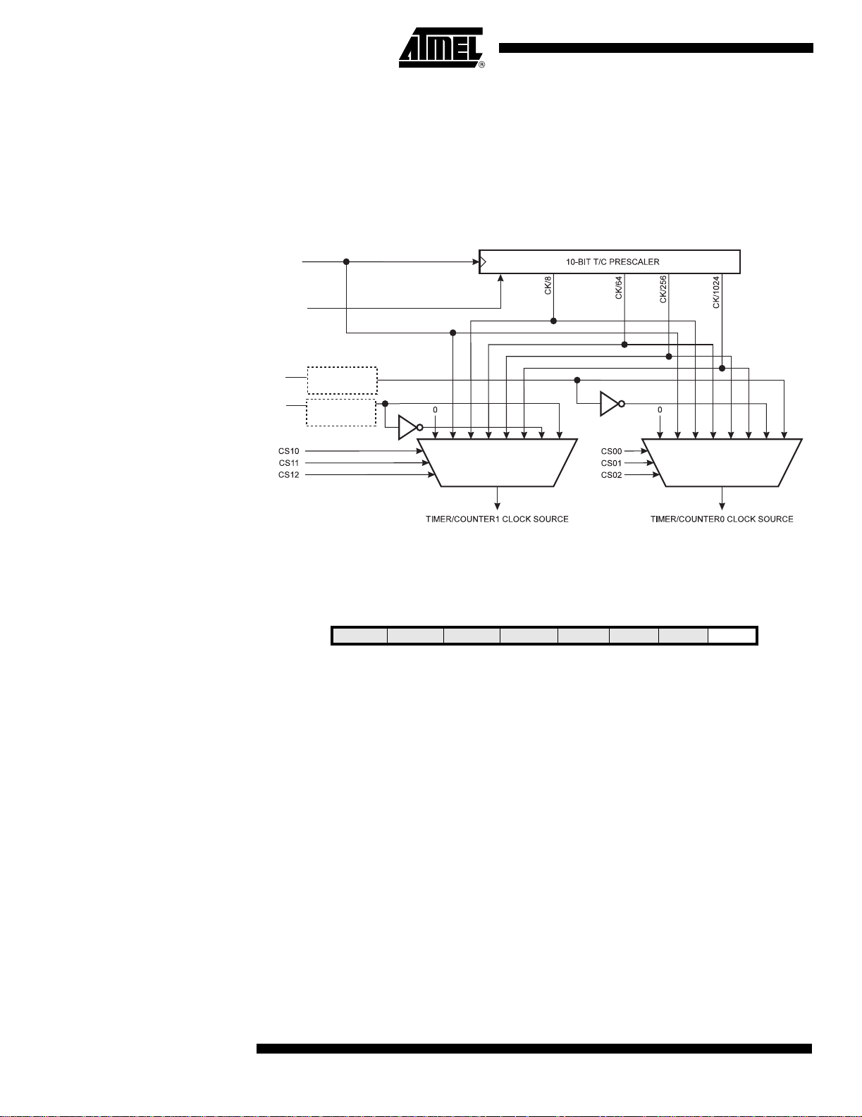
the edge detector uses sampling, the maximum frequency of an external clock it can
detect is half the sampling frequency (Nyquist sampling theorem). However, due to variation of the system clock frequency and duty cycle caused by Oscillator source (crystal,
resonator, and capacitor s) toleran ces, it is recommended t hat maximum frequency of an
external clock source is less than f
clk_I/O
/2.5.
An external clock source can not be prescaled.
General Timer/Counter Control Register – GTCCR
Figure 38. Prescaler for Timer/Counter0 and Timer/Counter1
clk
I/O
PSR10
T0
T1
Synchronization
Synchronization
clk
Clear
T1
(1)
clk
T0
Note: 1. The synchronization logic on the input pins (T1/T0) is shown in Figure 37.
Bit 7 6 5 4 3 2 1 0
— – – – – – — PSR10 GTCCR
Read/Write R R R R R R R/W R/W
Initial Value 0 0 0 0 0 0 0 0
82
• Bit 0 – PSR10: Prescaler Reset Timer/Counter1 and Timer/Counter0
When this bit is one, Timer/Counter1 and Timer/Counter0 prescaler will be Reset. This
bit is normally cleared immedia tely by hardwar e. Note that Time r/Counter1 and
Timer/Counter0 share the same prescaler and a reset of this prescaler will affect both
timers.
ATtiny2313
2543A–AVR–08/03
Page 83

ATtiny2313
16-bit Timer/Counter1
The 16-bit Timer/Counter unit allows accurate program execution timing (event management), wave generation, and signal timing measurement. The main features are:
True 16-bit Design (i.e., Allows 16-bit PWM)
•
• Two independent Output Compare Units
• Double Buffered Output Compare Registers
• One Input Capture Unit
• Input Capture Noise Canceler
• Clear Timer on Compare Match (Auto Reload)
• Glitch-free, Phase Correct Pulse Width Modulator (PWM)
• Variable PWM Period
• Frequency Generator
• External Event Counter
• Four independent interrupt Sources (TOV1, OCF1A, OCF1B, and ICF1)
Overview Most register and bit references in this section are written in general form. A lower case
“n” replaces the Timer/Counter number, and a lower case “x” replaces the Output Compare unit channel. However, when using the register or bit defines in a program, the
precise form must be used, i.e., TCNT1 for accessing Timer/Counter1 counter value
and so on.
A simplified bl ock dia gram of the 16-bit Timer/Co unter is sho wn in Fi gure 39 . For the
actual placement of I/O pins, refer to “Pinout ATtiny 2313” on page 1 . CPU acces sible
I/O Registers, including I/O bits and I/O pins, are shown in bold. The device-specific I/O
Register and b it locat ions a re list ed in the “16-bit Timer/C ount er Regis ter D escriptio n”
on page 105.
2543A–AVR–08/03
83
Page 84
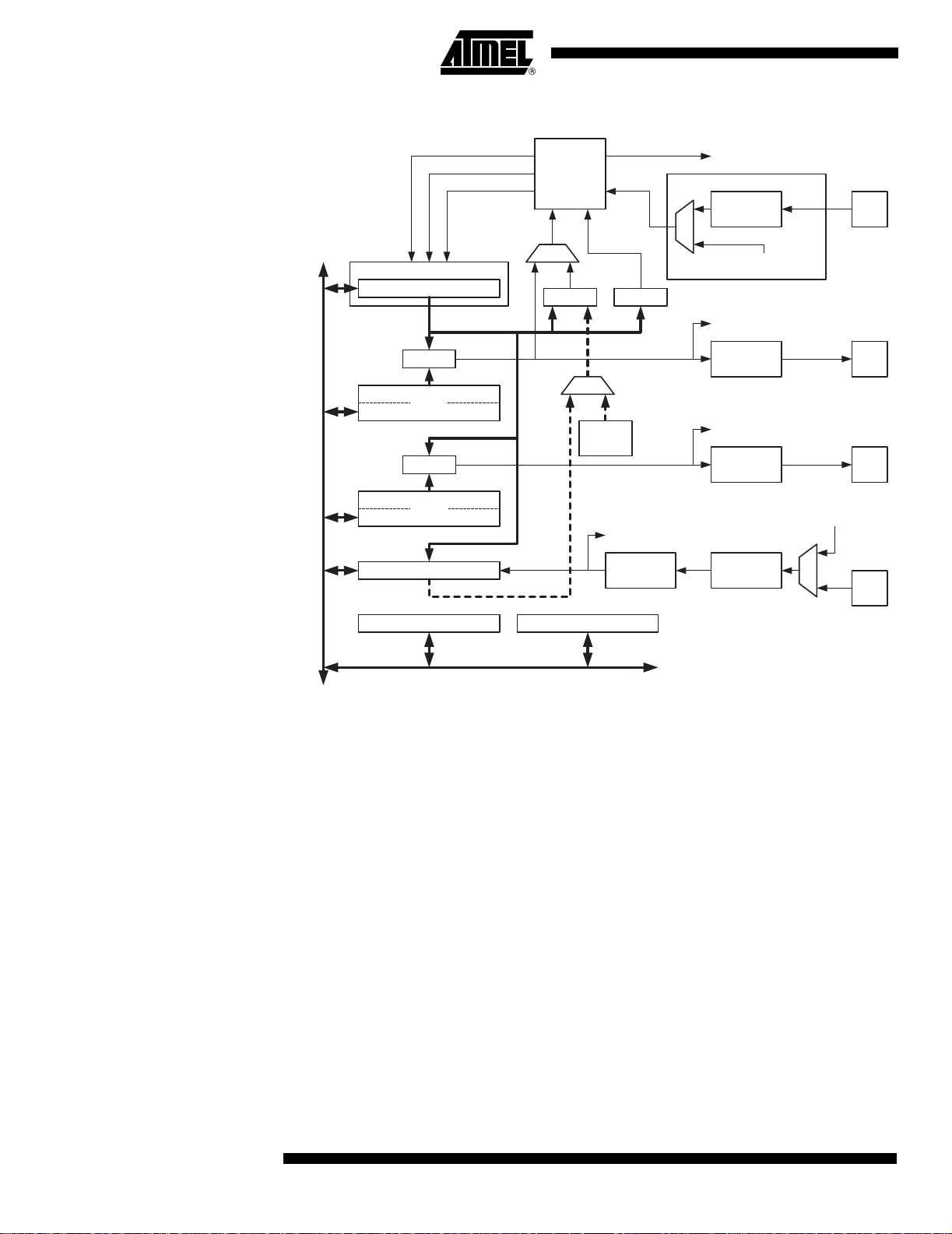
Figure 39. 16-bit Timer/Counter Block Diagram
(1)
Count
Clear
Direction
Timer/Counter
TCNTn
Control Logic
TOP BOTTOM
=
clk
Tn
= 0
=
OCRnA
Fixed
TOP
Values
=
DATA BUS
OCRnB
ICRn
ICFn (Int.Req.)
Edge
Detector
TOVn
(Int.Req.)
Clock Select
Edge
Detector
( From Prescaler )
OCnA
(Int.Req.)
Waveform
Generation
OCnB
(Int.Req.)
Waveform
Generation
Noise
Canceler
Tn
OCnA
OCnB
( From Analog
Comparator Ouput )
ICPn
TCCRnA TCCRnB
Note: 1. Refer to Figure 1 on page 1 for Timer/Counter1 pin placement and description.
Registers The Timer/Counter (TCNT1), Output Compare Registers (OCR1A/B), and Input Capture
Register (ICR1) are all 16-bit registers. Special p rocedures mu st be followed w hen
accessing the 16-bit registers. These procedures are described in the section “Accessing 16-bit Registers” on page 86. The Timer/Counter Control Register s (TCCR1A/B) are
8-bit registers and have no CPU access restrictions. Interrupt requests (abbreviated to
Int.Req. in the figure) signals are all visible in the Timer Interrupt Flag Register (TIFR).
All interrupts are individua lly m asked w ith th e T imer Interrup t Mask Register (TIMSK).
TIFR and TIMSK are not shown in the figure.
The Timer/Counter can be clocked internally, via the prescaler, or by an external clock
source on the T1 pin. The Cloc k Select logic block c ontrol s which cl ock sou rce and edge
the Timer/Counter uses to increment (or decrement) its value. The Timer/Counter is
inactive when no clock source is selected. The output from the Clock Select logic is
referred to as the timer clock (clk
).
1
T
The double buffered Output Co mpare Registers (OCR 1A/B) are compare d with the
Timer/Counter value at all t ime. The r esult o f the compar e can be use d by t he Wavef orm
Generator to generate a PWM or variable frequency output on the Output Compare pin
(OC1A/B). See “Output Compare Units” on p age 92. . Th e compare matc h event wi ll also
set the Compare M atch Flag (OCF1A/B ) which can be used to generate an Output
Compare interrupt request.
84
ATtiny2313
2543A–AVR–08/03
Page 85

ATtiny2313
The Input Capture Register can capture the Timer/Counter value at a given external
(edge triggered) event on either the Input Capture pin (ICP1) or on the Analog Comparator pins (See “Analog Comparator” on page 151.) The Input Capture unit includes a
digital filtering unit (Noise Canceler) for reducing the chance of capturing noise spikes.
The TOP value, or maximum Timer/Counter value, can in some modes of operation be
defined by either the OCR1A Register, the ICR1 Register, or by a set of fixed values.
When using OCR1A as TOP value in a PWM mode, the OCR1A Register can not be
used for generating a PWM output. However, the TOP value will in this case be double
buffered allowin g the TOP value to be changed i n run time. If a fixed TOP value is
required, the ICR1 Register can be used as an alternative, freeing the OCR1A to be
used as PWM output.
Definitions The following definitions are used extensively throughout the section:
Table 43. Definitions
BOTTOM The counter reaches the BOTTOM when it becomes 0x0000.
MAX The counter reaches its MAXimum when it becomes 0xFFFF (decimal 65535).
The counter reaches the TOP when it becomes equal to the highest value in the
TOP
count sequence. The TOP value can be assigned to be one of the fixed values:
0x00FF, 0x01FF, or 0x03FF, or to the value stored in the OCR1A or ICR1 Register. The assignment is dependent of the mode of operation.
Compatibility The 16-bit Timer/Count er has been updated and improved from pr evious versions of t he
16-bit AVR Timer/Counter. This 16-bit Timer/Counter is fully compatible with the earlier
version regarding:
• All 16-bit Timer/Counter related I/O Register address locations, including Timer
Interrupt Registers.
• Bit locations inside all 16-bi t Timer/Counter Registers, including Timer Interrupt
Registers.
• Interrupt Vectors.
The following control bits have changed name, but have same functionality and register
location:
• PWM10 is changed to WGM10.
• PWM11 is changed to WGM11.
• CTC1 is changed to WGM12.
The following bits are added to the 16-bit Timer/Counter Control Registers:
• FOC1A and FOC1B are added to TCCR1A.
• WGM13 is added to TCCR1B.
The 16-bit Timer/Counter has improvements that will affect the compatibility in some
special cases.
2543A–AVR–08/03
85
Page 86

Accessing 16-bit Registers
The TCNT1, OCR1A/B, and ICR1 are 16-bit registers that can be accessed by the AVR
CPU via the 8-bit data bus. The 16-bit register must be byte accessed using two read or
write operations. Each 16-bit timer has a single 8-bit register for temporary storing of the
high byte of the 16-bit access. The same temporar y register is shared between all 16-bit
registers within each 16-bi t timer. Acces sing the l ow byte trigger s the 16-bi t read or write
operation. When the low byte of a 16-bit register is written by the CPU, the high byte
stored in the temporary register, and the low byte written are both copied into the 16-bit
register in the same clock cycle. When the low byte of a 16-bit register is read by the
CPU, the high byte of the 16-bit register is copied into the temporary register in the
same clock cycle as the low byte is rea d.
Not all 16-bit accesses uses the temporary register for the high byte. Reading the
OCR1A/B 16-bit registers does not involve using the temporary register.
To do a 16-bit write , t he high byte must be written before the low byte. For a 16-bi t read,
the low byte must be read before the high byte.
The following code exampl es show how to access the 16-b it timer registers assum ing
that no interrupts updates the tem porary regis ter. The same princi ple can be used
directly for accessing the OCR1A/B and ICR1 Registers. Note that when using “C”, the
compiler handles the 16-bit access.
Assembly Code Examples
...
; Set TCNT1 to 0x01FF
ldi r17,0x01
ldi r16,0xFF
out TCNT1H,r17
out TCNT1L,r16
; Read TCNT1 into r17:r16
in r16,TCNT1L
in r17,TCNT1H
...
C Code Examples
unsigned int i;
...
/* Set TCNT1 to 0x01FF */
TCNT1 = 0x1FF;
/* Read TCNT1 into i */
i = TCNT1;
...
Note: 1. The example code assumes that the part specific header file is included.
For I/O Registers located in extended I/O map, “IN”, “OUT”, “SBIS”, “SBIC”, “CBI”,
and “SBI” instructions must be replaced with instructions that allow access to
extended I/O. Typically “LDS” and “S TS” combin ed with “S BR S”, “ SBRC”, “S BR”, a nd
“CBR”.
(1)
(1)
86
The assembly code example returns the TCNT1 value in the r17:r16 register pair.
It is important to notice that accessing 16-bit registers are atomic operations. If an inter-
rupt occurs between the two instructions accessing the 16-bit register, and the interrupt
code updates th e tempo rary register by acces sing th e sam e or an y other o f the 16-bit
timer registers, then the result of the access outside the interrupt will be corrupt ed.
ATtiny2313
2543A–AVR–08/03
Page 87

ATtiny2313
Therefore, when both the main code and the interrupt code update the temporary register, the main code must disable the interrupts during the 16-bit access.
The following code examples show how to do an atomic read of the TCNT1 Register
contents. Reading any of the OCR1A/B or ICR1 Registers can be done by using the
same principle.
Assembly Code Example
TIM16_ReadTCNT1:
; Save global interru pt flag
in r18,SREG
; Disable interrup ts
cli
; Read TCNT1 into r17:r16
in r16,TCNT1L
in r17,TCNT1H
; Restore global inte rrupt flag
out SREG,r18
ret
C Code Example
unsigned int TIM16_ReadTCNT1( void )
{
unsigned char sreg;
unsigned int i;
/* Save global interrupt flag */
sreg = SREG;
/* Disable interrupts */
_CLI();
/* Read TCNT1 into i */
i = TCNT1;
/* Restore global interrupt flag */
SREG = sreg;
return i;
}
(1)
(1)
2543A–AVR–08/03
Note: 1. The example code assumes that the part specific header file is included.
For I/O Registers located in extended I/O map, “IN”, “OUT”, “SBIS”, “SBIC”, “CBI”,
and “SBI” instructions must be replaced with instructions that allow access to
extended I/O. Typically “LDS” and “S TS” combin ed with “S BR S”, “ SBRC”, “S BR”, a nd
“CBR”.
The assembly code example returns the TCNT1 value in the r17:r16 register pair.
87
Page 88

The follow ing code ex amp les show h ow to do an atomic write of th e TCNT1 Regis ter
contents. Writing any of the OCR1A/B or I CR1 Registers can be done b y using the
same principle.
Assembly Code Example
TIM16_WriteTCNT1:
; Save global interru pt flag
in r18,SREG
; Disable interrup ts
cli
; Set TCNT1 to r17:r16
out TCNT1H,r17
out TCNT1L,r16
; Restore global inte rrupt flag
out SREG,r18
ret
C Code Example
void TIM16_WriteTCNT1( unsigned int i )
{
unsigned char sreg;
unsigned int i;
/* Save global interrupt flag */
sreg = SREG;
/* Disable interrupts */
_CLI();
/* Set TCNT1 to i */
TCNT1 = i;
/* Restore global interrupt flag */
SREG = sreg;
}
(1)
(1)
Reusing the Temporary High Byte Register
88
ATtiny2313
Note: 1. The example code assumes that the part specific header file is included.
For I/O Registers located in extended I/O map, “IN”, “OUT”, “SBIS”, “SBIC”, “CBI”,
and “SBI” instructions must be replaced with instructions that allow access to
extended I/O. Typically “LDS” and “S TS” combin ed with “S BR S”, “ SBRC”, “S BR”, a nd
“CBR”.
The assembly code example requires that the r17:r16 register pair contains the value to
be written to TCNT1.
If writing to more than on e 16- bit r egister wher e th e high byt e is t he same for a ll re gister s
written, then the high byte only needs to be written once. However, note that the same
rule of atomic operation described previously also applies in this case.
2543A–AVR–08/03
Page 89

ATtiny2313
Timer/Counter Clock Sources
The Timer/Counter can be clocked by an internal or an external clock source. The clock
source is selected by the Clock Select logic which is controlled by the Cl ock Select
(CS12:0) bits located in the Timer/Counter control Register B (TCCR1B). For details on
clock sources and prescaler, see “Timer/Counter0 and Timer/Co unter1 Pres calers” on
page 81.
Counter Unit The main part of the 16-bit Timer/Counte r is the programmable 16-bit bi-directional
counter unit. Figure 40 shows a block diagram of the counter and its surroundings.
Figure 40. Counter Unit Block Diagram
DATA BUS
TEMP (8-bit)
TCNTnH (8-bit) TCNTnL (8-bit)
TCNTn (16-bit Counter)
Signal description (i nternal signals):
Count Increment or decrement TCNT1 by 1.
(8-bit)
Count
Clear
Direction
Control Logic
TOP BOTTOM
TOVn
(Int.Req.)
clk
Tn
Clock Select
Edge
Detector
( From Prescaler )
Tn
Direction Select between increment and decrement.
Clear Clear TCNT1 (set all bits to zero).
clk
1
T
Timer/Counter clock.
TOP Signalize that TCNT1 has reached maximum value.
BOTTOM Signalize that TCNT1 has reached minimum value (zero).
The 16-bit counter is m apped into two 8 -bit I/O memory locati ons: Coun ter High
(TCNT1H) co ntai ning t he uppe r eigh t b its o f the coun ter, and Co unter Low (TCNT1L)
containing the lower eight bits. The TCNT1H Register can only be indirectly accessed
by the CPU. When the CPU does an access to the TCNT1H I/O location, the CPU
accesses the high b yte temporary register (T EMP). T he tempo rary reg ister is upd ated
with the TCNT1H value when the TCNT1L is read, and TCNT1H is updated with the
temporary register value when TCNT1L is written. This allows the CPU to read or write
the entire 16-bit counter value within one clock cycle via the 8-bit data bus. It is important to notice that there are special cases of writing to the TCNT1 Register when the
counter is counting that will give unpredictable results. The special cases are described
in the sections where they are of impor tance.
Depending on the mode of operation used, the counter is cleared, incremented, or decremented at each timer clock (clk
). The clk
1
T
can be generated from an external or
1
T
internal clock source, selected by the Cloc k Select bits (CS12:0). When no clock source
is selected (CS12:0 = 0) the timer is stopped. However, the TCNT1 value can be
accessed by the CPU, independent of whether clk
is present or not. A CPU write over-
1
T
rides (has priority over ) all counter clear or count operations.
2543A–AVR–08/03
The counting sequence is determined by the setting of the Waveform Generation mode
bits (WGM13:0) located in the Timer/Counter Control Registers A and B (TCCR1A and
TCCR1B). There are close connections between how the counter behaves (counts) and
89
Page 90

how waveforms are generated on the Output Compare outputs OC1x. For more details
about advanced counting sequences and waveform generation, see “Modes of Operation” on page 95.
The Timer/Counter Overflow Flag (TOV1) is set according to the mode of operation
selected by the WGM13:0 bits. TOV1 can be used for generating a CPU interrupt.
Input Capture Unit The Timer/Counter incorporates an Input Capture unit that can capture external events
and give them a time-stamp indicating time of oc currence. The external signal indicating
an event, or multiple events, can be applied via the ICP1 pin or alternatively, via the
analog-comparator unit . The ti me-stamps c an t hen be used t o calcul ate fr equency, dutycycle, and other features of the signal applied. Alternatively the time-stamps can be
used for creating a log of the events.
The Input Capture unit is illustrated by the block diagram shown i n Figure 41. The elements of the block diagram that are not directly a part of the Input Capture unit are gray
shaded. The small “n” in register and bit names indicates the Timer/Counter number.
Figure 41. Input Capture Unit Block Diagram
ICPn
WRITE
TEMP (8-bit)
ICRnH (8-bit)
ICRn (16-bit Register)
ACO*
Analog
Comparator
DATA BUS
ICRnL (8-bit)
ACIC* ICNC ICES
Noise
Canceler
(8-bit)
TCNTnH (8-bit) TCNTnL (8-bit)
TCNTn (16-bit Counter)
Edge
Detector
ICFn (Int.Req.)
When a change of the logic level (an event) occurs on the Input Capture pin (ICP1),
alternatively on the Analog Comparator output (ACO), and this change confirms to the
setting of the edge detector, a captur e will be triggered. Whe n a capture is triggered, the
16-bit value of the counter (TCNT1) is written to the Input Capture Register (ICR1). The
Input Capture Flag (ICF1) is set at the sam e system clock as the TCNT1 value is copied
into ICR1 Register. If enabled (ICIE1 = 1), th e Inp ut Cap ture Flag g enerates an Inp ut
Capture interrupt. The ICF1 flag is automatically cleared when the interrupt is executed.
Alternatively the ICF1 flag can be cleared by software by writing a logical one to its I/O
bit locati on.
90
Reading the 16-bit value in the Input Captur e Registe r ( ICR1) is done by fi rst r eading t he
low byte (ICR1L) and then the high byte (ICR1H). When the low byte is read the high
byte is copied into the high byte tempora ry regist er (TEMP). When the CPU reads the
ICR1H I/O location it will access the TEMP Register.
ATtiny2313
2543A–AVR–08/03
Page 91

ATtiny2313
The ICR1 Register can only b e written when usi ng a W aveform G enera tion mode that
utilizes the ICR1 Register for defining the coun ter’s TOP va lue. In thes e cases the
Waveform Generation mode (WGM13:0) bits must be set before the TOP value can be
written to the ICR1 Register. When writing the ICR1 Regis ter the high byte must be writ ten to the ICR1H I/O location before the low byte is written to ICR1L.
For more inform ation on how to ac cess the 16-bit regis ters refe r to “Acce ssing 16 -bit
Registers” on page 86.
Input Capture Trigger Source The main trigg er source for the Input Capture uni t is the Input Capture pin (ICP1).
Timer/Counter1 can al ternati vely use th e Ana log Comp arato r output as trigger source
for the Input Capture unit. The Analog Comparator is selected as trigger source by setting t he Analog Comparator Input Capture (ACIC) bit in the Analog Comparator Control
and Status Register (ACSR). Be aware that changi ng trigger source can trigger a ca pture. The Input Capture Flag must therefore be cleared after the change.
Both the Input Capture pin (ICP1) and the Analog Comparator output (ACO) inputs are
sampled using the same technique as for the T1 pin (Figure 37 on page 81). The edge
detector is also identical. However, when the noise canceler is enabled, additional logic
is inserted before the edge detector, which increases the delay by four system clock
cycles. Note tha t the input of the noise cancel er and edge dete ctor is always enabled
unless the Timer/Counter is set in a Waveform Generation mode that uses ICR1 to
define TOP.
An Input Capture can be triggered by soft ware by controlling the port of the ICP1 pin.
Noise Canceler The noise canceler improves noise immunity by using a simple digital filtering scheme.
The noise canceler input is monitored over four samples, and all four must be equal for
changing the output that in turn is used by the edge detector.
The noise canceler is enabled by setting the Input Capture Noise Canceler (ICNC1) bit
in Timer/Counter Control Register B (TCCR1B). When enabled the noise canceler intro-
duces additional four system clock cycles of delay from a change applied to the input, to
the update of t he ICR1 Register. The noise canceler uses the system clock and is therefore not affected by the prescaler.
Using the Input Capture Unit The main chal lenge wh en using the Input Ca pture un it is to assign enough pro cessor
capacity for handling the incoming events. The time between two events is critical. If the
processor has not read the captured value in the ICR1 Register before the next even t
occurs, the ICR1 will be overwritten with a new value. In this case the result of the capture will be incorrect.
When using the Input Capt ure int errupt , the ICR1 Regi st er shoul d be read as earl y in t he
interrupt handler routine as possible. Even though the Input Capture interrupt has relatively high priority, the maximum interrupt response time is dependent on the maximum
number of clock cycles it takes to hand le any of the other interrupt requests.
Using the Input Capture unit in any mode of operation when the TOP value (resolution)
is actively changed during oper ati on, is not recommended.
Measurement of an external sig nal’s duty cy cle require s that th e trigg er edge is changed
after each capture. Changing the edge sensing must be done as early as possible after
the ICR1 R egist er h as be en read. Aft er a c hang e of the edge , the Inpu t C apture Fl ag
(ICF1) must be cleared by software (writing a logical one to the I/O bit location). For
measuring frequency only, the clearing of the ICF1 flag is not required (if an interrupt
handler is used).
2543A–AVR–08/03
91
Page 92
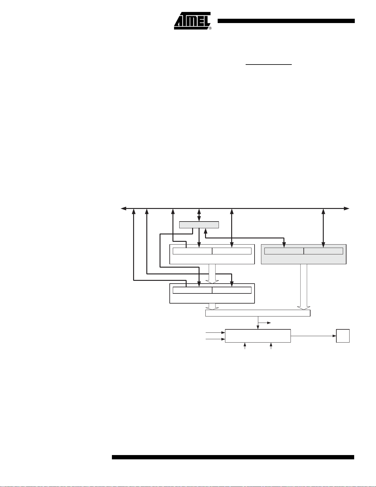
Output Compare Units The 16-bit comparator continuously compares TCNT1 with the Output Compare Regis-
ter (OCR1x). If TCNT equa ls OCR1x the com parator signals a match. A m atch will set
the Output Compare Flag (OC F1x) at the next timer clock cycle
1), the Output Compare Flag g ener ates an Outp ut Compare inte rrupt. The OCF1x fl ag is
automatically cleared wh en the in terrupt is executed. Al ternatively th e OCF1 x flag can
be cleared by software by wr itin g a logic al one to it s I/O bi t locat ion. The Waveform Gen erator uses the match signal to generate an output according to operating mode set by
the Waveform Generation mode (WGM13:0) bits and Compare Output mode
(COM1x1:0) bits. The TOP and BOTTOM signals are used by the Waveform Generator
for handling the special cases of the extreme values in some modes of operation (See
“Modes of Operation” on page 95.)
A special featu re o f Output Com pare u nit A allow s it to define the Timer/ Counte r TO P
value (i.e., counter resolut ion). In addition t o the counter resoluti on, the TOP value
defines the period time for wavef orms generated by the Waveform Generator.
Figure 42 shows a blo ck diagram of the Output Compare unit. The small “n” i n the register and bit names indicates the device number (n = 1
for Timer/Counter 1), and the “x”
indicates Output Compare unit (A/B). The elements of the block diagram that are not
directly a part of the Output Compare unit are gray shaded.
Figure 42. Output Compare Unit, Block Diagram
DATA BUS
TEMP (8-bit)
(8-bit)
. If enabled (OCIE1x =
OCRnxH Buf. (8-bit)
OCRnx Buffer (16-bit Register)
OCRnxH (8-bit) OCRnxL (8-bit)
OCRnx (16-bit Register)
TOP
BOTTOM
OCRnxL Buf. (8-bit)
=
(16-bit Comparator )
Waveform Generator
TCNTnH (8-bit) TCNTnL (8-bit)
TCNTn (16-bit Counter)
OCFnx (Int.Req.)
OCnx
COMnx1:0WGMn3:0
The OCR1x Register is double buff ered when using any of the twelve Pulse Width Modulation (P WM) modes. F or the Norma l and Clear Timer on Compare (CTC) mo des of
operation, the double buffering is disabled. The double buffering synchronizes the
update of the OCR1x Com pare Register to ei ther TOP or BOTT OM of the count ing
sequence. The synchronizat ion prevent s the occurre nce of odd-leng th, non-sy mmetrical
PWM pulses, thereby making the output glitch-free.
The OCR1x Register access may seem complex, but this is not case. When the double
buffering is enabled, the CPU has access to t he OCR1x Buf fer Register, and if double
buffering is disabl ed the CPU will access the OCR1x dir ectly. The content of the OCR1x
92
ATtiny2313
2543A–AVR–08/03
Page 93

ATtiny2313
(Buffer or Compare) Register is only changed by a write op eration (the Timer/C ounter
does not update this register auto matical ly as the TCNT1 and ICR1 Registe r). Therefor e
OCR1x is not re ad via the hi gh byte tem pora ry register (TE MP). How ever, it is a g ood
practice to read the low byte first as when accessing other 16 -bit registers. Writing the
OCR1x Registers must be done via the TEMP Register since the compare of all 16 bits
is done continuously. The high byte (OCR1xH) has to be written first. When the high
byte I/O location is written by the CPU, the TEMP Register will be updated by the value
written. Then when the low byte (OCR1xL) i s writt en to the l ower eight bits, the hi gh byte
will be copied into the upper 8-bits of either the OCR1x buffer or OCR1x Compare Register in the same system clock cycle.
For more information of how to access the 16-bit registers refer to “Accessing 16-bit
Registers” on page 86.
Force Output Compare In non-PWM Waveform Generation modes, the match output of the comparator can be
forced by writing a one to the Force Output Compare (FOC1x) bit. Forcing compare
match will not set the OCF1x flag or reload/clear the timer, but the OC1x pin will be
updated as if a real compare match had occurred (the COM11:0 bits settings define
whether the OC1x pin is set, cleared or toggled).
Compare Match Blocking by TCNT1 Write
Using the Output Compare Unit
All CPU writes to the TCN T1 Register will bl ock any compa re match that occurs in the
next timer clock cycl e, even when the timer is stopped. This feature allows OCR1x to be
initialized to the same value as TCNT 1 without triggeri ng an interrupt when th e
Timer/Counter clock is enabled.
Since writing TCNT 1 in any m ode o f o peratio n will block al l com pare m atch es for o ne
timer clock cycle, there are risks involved when changing TCNT1 when using any of the
Output Compare channels, independent of whet her the Timer/Counter is running or not.
If the value written to TCNT1 equals the OCR1x value, the compare match will be
missed, resulting in incorrect waveform generation. Do not write the TCNT1 equal to
TOP in PWM modes with variable TOP values. The compare match for the TOP will be
ignored and the counter will contin ue to 0xFFFF. Similarl y, do not wr ite the TCNT1 val ue
equal to BOTTOM when the counter is downcounting.
The setup of the OC1x should be performed before setting the Data Direction Register
for the port pin to output. The easiest way of setting the OC1x value is to use the Force
Output Compare (FOC1x) strobe bits in Normal mode. The OC1x Register keeps its
value even when changing between Waveform Generation modes.
Be awar e that the CO M1x1 :0 bits are n ot dou ble bu ffer ed toge ther with th e co mpare
value. Changing the COM1x1:0 bits will take effect immediately.
2543A–AVR–08/03
93
Page 94

Compare Match Output Unit
The Compare Output mode (COM1x1:0) bits have two functions. The Waveform Generator uses the COM1x1:0 bits for defining the Output Compare (OC1x) state at the next
compare match. Secondly the COM1x1:0 bits control the OC1x pin output source. Figure 43 shows a simplified sch ematic of t he logic affected by the COM1 x1:0 bit set ting.
The I/O Registers, I/O bits, and I/ O pins in the figure are shown in bold. Only the parts of
the genera l I/O port contro l registers ( DDR and PORT ) that are affec ted by the
COM1x1:0 bits are shown. When referring to the OC1x state, the reference is for the
internal OC1x Register, not the OC1x pin. If a system reset occur, the OC1x Register is
reset to “0”.
Figure 43. Compare Match Output Unit, Schematic
COMnx1
COMnx0
FOCnx
Waveform
Generator
DQ
OCnx
1
0
OCnx
Pin
DQ
PORT
DATA BUS
DQ
DDR
clk
I/O
The general I/O port function is overridden by the Output Compare (OC1x) from the
Waveform Generator if either of the COM1x1:0 bits are set. However, the OC1x pin
direction (input or output) is still controlled by the Data Direction Register (DDR) for the
port pin. The Data Direction Register bit for the OC1x pin (DDR_OC1x) must be set as
output before the OC1x value i s visi ble on the pin. The port overri de funct ion is ge nerall y
independent of the Waveform Generation mode, but there are some exceptions. Refer
to Table 44, Table 45 and Table 46 for details.
The design of the Output Compare pin logic all ows initial izat ion of the OC1x stat e before
the output is enabled. Note th at some COM 1x1:0 bit settings ar e reserved for certa in
modes of operation. See “16-bit Time r/Counter Register Description” on page 105.
The COM1x1:0 bits have no effect on the Input Capture unit.
94
ATtiny2313
2543A–AVR–08/03
Page 95

ATtiny2313
Compare Output Mode and Waveform Generation
The Waveform Generator uses the COM1x1:0 bits different ly in normal, CTC, and PWM
modes. For all modes, setting the COM1x1:0 = 0 tells the Waveform Generator that no
action on the OC1x Regi ster is to be performed on the nex t comp are match. For co mpare output actions in the non-PWM modes refer to Table 44 on page 105. For fast
PWM mode refer to T able 45 on page 105, and for phas e correct an d phase an d frequency correct PWM refer to Table 46 on page 107.
A change of the COM1x1:0 bits state will have effect at t he first compare match after the
bits are writt en. For non-PWM modes, the action can be forced to have immedi ate effect
by using the FOC1x strobe bits.
Modes of Operation The mode of operation, i .e. , t he behavior of the Timer/Counter and the Output Compare
pins, is defined by the combination of the Waveform Generation mode (WGM13:0) and
Compare Output mode (COM1x1:0) bits. The C ompare Output mode bits do not affect
the counting sequence, w hile the W aveform Ge neration m ode bits d o. The CO M1x1:0
bits control whe ther the PWM output gene rated sho uld be invert ed or not (inver ted or
non-inverted PWM). For non-PWM modes the COM1x1:0 b its control wh ether the output should be set, cleared or toggle at a compare match (See “Compare Match Output
Unit” on page 94.)
For detailed timing information refer to “Timer/Counter Timing Diagrams” on page 103.
Normal Mode The simplest mo de of operat ion is the No rmal mode (WGM13:0 = 0). In this mode the
counting direction is always up (incrementing), and no counter clear is performed. The
counter simply overruns when it passes its maximum 16-bit value (MAX = 0xFFFF) and
then restarts from the BOTTOM (0x0000). In normal operation the Timer/Counter Over-
flow Flag (TOV1) will be set in the same timer clock cycle as the TCNT1 becomes zero.
The TOV1 flag in this case behaves like a 17th bit, except that it is only set, not cleared .
However, combined with the timer overflow interrupt that automatically clears the TOV1
flag, the timer resolution can be increa sed by software. There are no spe cial cases to
consider in the Normal mode, a new counter value can be written anytime.
The Input Capture unit is easy to use in Normal mode. However, observe that the maximum interval between the ext ernal events must not excee d the resolut ion of the count er.
If the interval between events are too long, the timer overflow interrupt or the prescaler
must be used to extend the resolution for the capt ure unit.
The Output Compare units can be used to gener ate in terrup ts at some given t ime. Usi ng
the Output Compare t o generate wavefo rms in Normal mode is not recom mended,
since this will occupy too much of the CPU time.
2543A–AVR–08/03
95
Page 96
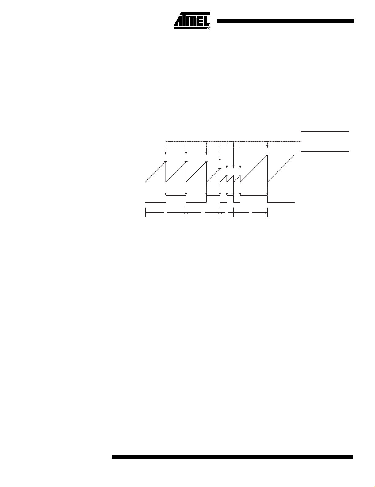
Clear Timer on Compare
f
Match (CTC) Mode
In Clear Timer on Comp are or CTC mode (WGM1 3:0 = 4 or 12), the OCR1 A or ICR1
Register are used to manipulate the counter resolution. In CTC mode the counter is
cleared to zero when the counter value (TCNT1) matches ei ther the OCR1A (WGM13:0
= 4) or the ICR1 (WGM13:0 = 12). The OCR1A or ICR1 define the top value for the
counter, hence also its resolution. This mode allows greater control of the compare
match output frequency. It also simplifies the operation of counting external events.
The timing diagram for the CTC mode is shown in Figure 4 4. The counter value
(TCNT1) increases until a compare match occurs with either OCR1A or ICR1, and then
counter (TCNT1) is cleared.
Figure 44. CTC Mode, Timing Diagram
OCnA Interrupt Flag Set
or ICFn Interrupt Flag Set
(Interrupt on TOP)
TCNTn
OCnA
(Toggle)
Period
1 4
2 3
(COMnA1:0 = 1)
An interrupt can be generated at each time the counter value reaches the TOP value by
either using the OCF 1A or ICF1 flag acc ording to the registe r used to defin e the TOP
value. If the interrupt is enabled, the interrupt handler routine can be used for updating
the TOP value. However, changing the TOP to a value close to BOTTOM when the
counter is running with none or a low prescaler value must be done with care since the
CTC mode does n ot have t he doub le buffer ing feat ure. If the new va lue writ ten to
OCR1A or ICR1 is lower than the cur rent value of TCNT1, the co unter wi ll miss the compare match. The counter will then have to count to its maximum value (0xFFFF) and
wrap around starting at 0x0000 before the compare match can occur. In many cases
this feature is not desirable. An alternative will then be to use the fast PWM mode using
OCR1A for defining TOP (WGM13:0 = 15) since t he OCR1A then will be double
buffered.
For generating a waveform output in CTC mode, the OC1A output can be set to toggle
its logical level on each c ompare mat ch by sett ing the Compar e Output mode bi ts to tog gle mode (COM1A1:0 = 1). The OC1A value will not be visible on the port pin unless the
data direction f or the pin is set to output (DDR_OC1A = 1). The waveform generated will
have a maximum frequency of f
OC1A
= f
/2 when OCR1A is set to zero (0x0000). The
clk_I/O
waveform frequency is defined by the foll owing equation:
f
OCnA
-------------------------------------------------- -=
2 N 1 OCRnA+()⋅⋅
clk_I/O
The N variable represents t he prescaler factor (1, 8, 64, 256, or 1024).
As for the Normal mode of operation, the TOV1 flag is set in the same timer clock cycle
that the counter counts from MAX to 0x0000.
96
ATtiny2313
2543A–AVR–08/03
Page 97
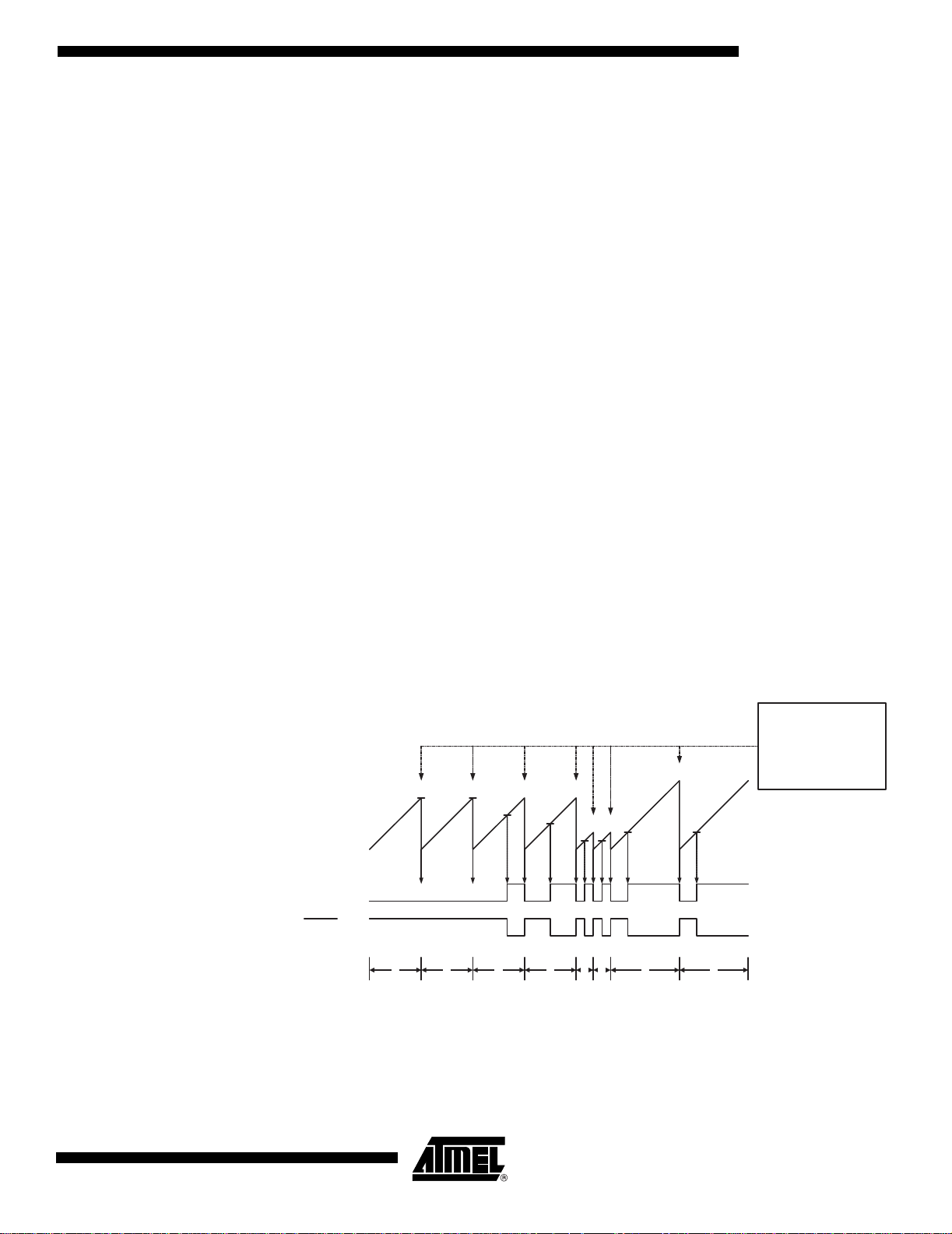
ATtiny2313
Fast PWM Mode The fast Pulse Width Modu lat ion or fast PWM mode (WGM13:0 = 5, 6, 7, 14, or 15) pro -
vides a high frequency PWM waveform generation option. The fast PWM differs from
the other PWM options by its single-slope operation. The counter counts from BOTTOM
to TOP then restarts from BOTTOM. In non-inverti ng Compare Outp ut mode, the Output
Compare (OC1x) is set on the compare match between TCNT1 and OCR1x, and
cleared at TOP. In inverting Compare Output mode output is cleared on compare match
and set at TOP . Due to the sing le-slope operat ion, the operati ng fr equency of the fast
PWM mode can be twice as high as the phase correct and phase and frequency correct
PWM modes tha t u se du al-slop e ope rati on. Th is h igh frequ ency makes the fa st PW M
mode well suited for power regulation, rectification, and DAC applications. High frequency allows physically small sized external components (coils, capacitors), hence
reduces total system cost.
The PWM resolution for fast PWM can be fixed to 8-, 9-, or 10-bit, or defined by either
ICR1 or OCR1A. The minimum resolution allowed is 2-bit (ICR1 or OCR1A set to
0x0003), and the maximum resolution is 16-bit (ICR1 or OCR1A set to MAX). The PWM
resolution in bits can be calcula ted by usi ng the following equation:
TOP 1+()log
R
FPWM
In fast PWM mode the counter is incremented until the counter value matches either
one of the fixed values 0x00FF, 0x01FF, or 0x03FF (WGM13:0 = 5, 6, or 7), the value in
ICR1 (WGM13:0 = 14), or th e va lue in O CR1A (W GM1 3:0 = 15 ). Th e coun ter is then
cleared at the following timer clock cycle. The timing diagram for the fast PWM mode is
shown in Figure 45. The figure shows fast PWM mode when OCR1A or ICR1 is used to
define TOP. The TCNT1 value is i n the tim ing diagram show n as a hi stogram for i llustrating the single-sl ope operat ion . The diagram inc ludes non- invert ed and invert ed PWM
outputs. The small horizontal line marks on the TCNT1 slopes represent compare
matches between OCR1x and TCNT1. The OC1x interrupt flag will be set when a compare match occurs.
---------------------------------- -=
2()log
Figure 45. Fast PWM Mode, Timing Diagram
OCRnx/TOP Update and
TOVn Interrupt Flag Set and
OCnA Interrupt Flag Set
or ICFn Interrupt Flag Set
(Interrupt on TOP)
TCNTn
OCnx
OCnx
Period
1 7
2 3 4 5 6 8
(COMnx1:0 = 2)
(COMnx1:0 = 3)
The Timer/Counter Overflow Flag (TOV1) is set each time the counter reaches TOP. In
addition the OC1A or IC F1 flag is set at the same timer clock cycle as TOV1 is set when
either OCR1 A or ICR1 i s used for defi ning th e TOP val ue. If one of th e interrup ts are
enabled, the interrupt h andler routine ca n be us ed fo r upd ating the TOP and com pare
values.
2543A–AVR–08/03
97
Page 98

When changing the TOP value the program must ensure that the new TOP value is
f
higher or equal t o the val ue of all of t he Co mpare R egisters . If the TOP value i s lower
than any of the Compare Registers, a compare match will never occur between the
TCNT1 and the OCR1x. Note that when using fixed TOP values the unused bits are
masked to zero when any of the OCR1x Registers are written.
The procedure for updating ICR1 differs from updating OCR1A when used for defining
the TOP value. The ICR1 Register is not double buffered. This means that if ICR1 is
changed to a low value when the counter is running with none or a low prescaler value,
there is a risk that the new ICR1 value written is lower than the current value of TCNT1.
The result will then be that the counter w ill miss the compare ma tch at t he TOP va lue.
The counter will then have to count to the MAX value (0xFFFF) and wrap around starting at 0x0000 before the compare m atch can occur. The O CR1A R egister how ever, is
double buffered. This feature allow s the OCR1A I/O locat ion to be wr itten anytime.
When the OCR1A I/O location is wri tten the value written will be put in to the OCR1A
Buffer Registe r. Th e OCR 1A C ompa re Regi ster w ill th en be upd ated w ith the valu e in
the Buffer Register at t he next timer c lock cycl e the TCNT1 ma tches TOP. The upda te i s
done at the same timer clock cycle as the TCNT1 is cleared and the TOV1 flag is set.
Using the ICR1 Register for defining TOP works well when using fixed TOP values. By
using ICR1, the OCR1A Register is free to be used for generating a PWM output on
OC1A. However, if the base PWM frequency is actively changed (by changing the TOP
value), using the OCR1 A as TOP is clearly a better cho ice due to its doub le buffe r
feature.
In fast PWM mode , the compare uni ts allow genera tion of PWM wa veforms on the
OC1x pins. Setting the COM1x1:0 bits to two will produce a non-inverted PWM and an
inverted PWM output can be generate d by setting the COM1x1:0 to three (see Table on
page 105). The actual OC1x value will only be visible on the port pin if the data di rection
for the port pin is set as output (DDR_OC1x). The PWM waveform is generated by setting (or clearing) the OC1x Regi ster at the compare matc h between OCR1x and TCNT1,
and clearing (or setting) the OC1x Register at the timer clock cycle the counter is
cleared (changes from TOP to BOTTOM).
The PWM frequency for the output can be calculated by the following equation:
f
clk_I/O
OCnxPWM
---------------------------------- -=
N 1 TOP+()⋅
The N variable represents the prescaler divider (1, 8, 64, 256, or 1024).
The extreme values for the OCR1x Register represents special cases when generating
a PWM waveform output in the fast PWM mode. If the OCR1x is set equal to BOTTOM
(0x0000) the output will be a narrow spike for eac h TOP+1 t imer clock cycle. Setting the
OCR1x equal to TOP will result i n a constant high or low output (dependi ng on the pol arity of the output set by the COM1x1:0 bits.)
A frequency (with 50% duty cycle) wavef orm output in fast PWM mode can be achieved
by setting OC1A to toggle its logical level on each compare match (COM1A1:0 = 1). The
waveform generated will have a maximum frequency of f
OC1A
= f
/2 when OCR1A is
clk_I/O
set to zero (0x0000). This feat ure is simila r to the OC1A toggle in CTC mode, except the
double buffer feature of the Output Compare unit is enabled in the fast PWM mode.
98
ATtiny2313
2543A–AVR–08/03
Page 99

ATtiny2313
Phase Correct PWM Mode The phase correct Pulse W idth Modulation or phase correct PWM mode (WGM13:0 = 1,
2, 3, 10, or 11) provides a high resolution phase correct PWM waveform generation
option. The phase correct PWM mode is, like the phase and frequency correct PWM
mode, based on a dual-slope operation. The counter counts repeatedly from BOTTOM
(0x0000) to TOP and then from TOP to BOTTOM. In non-inverting Compare Output
mode, the Output Co mpare (OC1 x) is cle ared on the com pare mat ch between TCNT1
and OCR1x while upcounting, and set on the compare match while downcounting. In
inverting Output Compare mode, the oper ation i s invert ed. The dual -slope operat ion has
lower maximum o peration freque ncy th an singl e slope op eration. How ever, due to the
symmetric feature of the dual-slope PWM modes, these modes are preferred for motor
control applications.
The PWM resolution for the phase corre ct PWM mode can be fixed to 8- , 9-, or 10- bit, or
defined by either ICR1 or OCR1A. The minimum resolution allowed is 2-bit (ICR1 or
OCR1A set to 0x0003), and the maximum resolution is 16-bit (ICR1 or OCR1A set to
MAX). The PWM resolution in bits can be calculated by using the following equation:
TOP 1+()log
R
PCPWM
In phase correct PWM mode th e counter is incremented u nti l the counter value matches
either one of the fixed values 0x00FF, 0x01FF, or 0x03FF (WGM13:0 = 1, 2, or 3), the
value in ICR1 (WGM13:0 = 10), o r the value in OCR1A (WGM13:0 = 11). The counter
has then reache d th e TOP a nd changes the count d irection. The TCNT 1 val ue wil l be
equal to TOP for one timer clock cycle. The timing diagram for the phase correct PWM
mode is shown on Figure 46. The fi gure shows phase corr ect PWM mode when OCR1A
or ICR1 is used t o defin e TOP. The TC NT1 val ue is i n the tim ing di agram sh own as a
histogram for i llustrating the dual-slo pe oper ation. Th e diagram inc ludes no n-invert ed
and inverted PWM outputs. The sma ll horizontal line marks on the TCNT1 slopes represent compare matches between OCR1x and TCNT1. The OC1x interrupt flag will be set
when a compare match occurs.
---------------------------------- -=
2()log
Figure 46. Phase Correct PWM Mode, Timing Diagram
TCNTn
OCnx
OCnx
Period
1 2 3 4
OCRnx/TOP Update and
OCnA Interrupt Flag Set
or ICFn Interrupt Flag Set
(Interrupt on TOP)
TOVn Interrupt Flag Set
(Interrupt on Bottom)
(COMnx1:0 = 2)
(COMnx1:0 = 3)
2543A–AVR–08/03
99
Page 100

The Timer/Counter Overflow Flag (TOV1) is set each time the counter reaches BOTTOM. When either OCR1A or ICR1 is used for defining the TOP value, the OC1A or
ICF1 flag is set accordingly at the same timer clock cycle as the OCR1x Re gisters are
updated with the doubl e buffer value (at TOP). The interrupt flags c an be used to generate an interrupt each time the counter reaches the TOP or BOTTOM value.
When changing the TOP value the program must ensure that the new TOP value is
higher or equal t o the val ue of all of t he Co mpare R egisters . If the TOP value i s lower
than any of the Compare Registers, a compare match will never occur between the
TCNT1 a nd the OC R1x. Note t hat when using fixed T OP val ues, the unus ed bits are
masked to zero when any of the OCR1x Registers are writt en. As the third period shown
in Figure 46 illustrates, changing the TOP actively while the Timer/Counter is running in
the phase correct mode can result in an unsymmetrical output. The reason for this can
be found in the time of update of the OCR1x Register. Since the OCR1x update occurs
at TOP, the PWM period starts and ends at TOP. This implies that the length of the falling slope is d eter m ined by the previous TOP value, while the l ength of the risi ng slope is
determined by the new TOP value. W hen these two values differ the two slopes of the
period will differ in length. The difference in leng th gi ves the unsymmetrical result on the
output.
It is recommended to use the phas e and freq uency correct mode instead of the phase
correct mode when changing the TOP value while the Timer/Counter is running. When
using a static TOP value there are practically no differences between the two modes of
operation.
In phase correct PWM mode, the compar e unit s allow g enera tion of PWM wave forms on
the OC1x pins. Setting the COM1x1:0 bits to two will produce a non-inverted PWM and
an inverted PWM output can be generated by setting the COM1x1:0 to three (See Table
on page 107). Th e actual OC1x value will only be visible on t he port pin if the data direction for the port pin is set as output (DDR_OC1x). The PWM waveform is generated by
setting (or clearing) the OC1x Register at the com pare match between OCR1 x and
TCNT1 when the counter increments, and clearing (or setting) the OC1x Register at
compare match between OCR1x and TCNT1 when the counter decrements. The PWM
frequency for the outpu t w hen usin g p hase co rrect PW M can be ca lculat ed by the following equation:
f
clk_I/O
f
OCnxPCPWM
----------------------------=
2 NTOP⋅⋅
100
The N variable represents the prescaler divider (1, 8, 64, 256, or 1024).
The extreme values for the OCR1x Register represent special cases when generating a
PWM waveform output in the phase correct PWM m ode. If the OCR1x is set equal to
BOTTOM the output will be continu ously low and if set equal t o TOP the output will be
continuously high for non-inverted PW M mo de. For inverted PWM the output w ill have
the opposite logic values.
ATtiny2313
2543A–AVR–08/03
 Loading...