

Page 1

Features
• Utilizes the AVR
• High-performance and Low-power 8-bit RISC Architecture
– 90 Powerful Instructions – Most Single Clock Cycle Execution
– 32 x 8 General Purpose Working Registers
– Up to 8 MIPS Throughput at 8 MHz
• Nonvolatile Program and Data Memory
– 1K Byte of Flash Program Memory
In-System Programmable (ATtiny12)
Endurance: 1,000 Write/Erase Cycles (ATtiny11/12)
– 64 Bytes of In-System Programmable EEPROM Data Memory for ATtiny12
Endurance: 100,000 Write/Erase Cycles
– Programming Lock for Flash Program and EEPROM Data Security
• Peripheral Features
– Interrupt and Wake-up on Pin Change
– One 8-bit Timer/Counter with Separate Prescaler
– On-chip Analog Comparator
– Programmable Watchdog Timer with On-chip Oscillator
• Special Microcontroller Features
– Low-power Idle and Power-down Modes
– External and Internal Interrupt Sources
– In-System Programmable via SPI Port (ATtiny12)
– Enhanced Power-on Reset Circuit (ATtiny12)
– Internal Calibrated RC Oscillator (ATtiny12)
• Specification
– Low-power, High-speed CMOS Process Technology
– Fully Static Operation
• Power Consumption at 4 MHz, 3V, 25°C
– Active: 2.2 mA
– Idle Mode: 0.5 mA
– Power-down Mode: <1 µA
• Packages
– 8-pin PDIP and SOIC
• Operating Voltages
– 1.8 - 5.5V for ATtiny12V-1
– 2.7 - 5.5V for ATtiny11L-2 and ATtiny12L-4
– 4.0 - 5.5V for ATtiny11-6 and ATtiny12-8
• Speed Grades
– 0 - 1.2 MHz (ATtiny12V-1)
– 0 - 2 MHz (ATtiny11L-2)
– 0 - 4 MHz (ATtiny12L-4)
– 0 - 6 MHz (ATtiny11-6)
– 0 - 8 MHz (ATtiny12-8)
®
RISC Architecture
8-bit
Microcontroller
with 1K Byte
Flash
ATtiny11
ATtiny12
Pin Configuration
ATtiny11
PDIP/SOIC
(RESET) PB5
(XTAL1) PB3
(XTAL2) PB4
GND
1
2
3
4
8
7
6
5
VCC
PB2 (T0)
PB1 (INT0/AIN1)
PB0 (AIN0)
(RESET) PB5
(XTAL1) PB3
(XTAL2) PB4
GND
ATtiny12
PDIP/SOIC
1
2
3
4
8
7
6
5
VCC
PB2 (SCK/T0)
PB1 (MISO/INT0/AIN1)
PB0 (MOSI/AIN0)
Rev. 1006C–09/01
1
Page 2

Description The ATtiny11/12 is a low-power CMOS 8-bit microcontroller based on the AVR RISC
architecture. By executing powerful instructions in a single clock cycle, the ATtiny11/12
achieves throughputs approaching 1 MIPS per MHz, allowing the system designer to
optimize power consumption versus processing speed.
The AVR core combines a rich instruction set with 32 general-purpose working registers. All the 32 registers are directly connected to the Arithmetic Logic Unit (ALU),
allowing two independent registers to be accessed in one single instruction executed in
one clock cycle. The resulting architecture is more code efficient while achieving
throughputs up to ten times faster than conventional CISC microcontrollers.
Table 1. Parts Description
Device Flash EEPROM Register Voltage Range Frequency
ATtiny11L 1K - 32 2.7 - 5.5V 0-2 MHz
ATtiny11 1K - 32 4.0 - 5.5V 0-6 MHz
ATtiny12V 1K 64 B 32 1.8 - 5.5V 0-1.2 MHz
ATtiny12L 1K 64 B 32 2.7 - 5.5V 0-4 MHz
ATtiny12 1K 64 B 32 4.0 - 5.5V 0-8 MHz
ATtiny11 Block Diagram The ATtiny11 provides the following features: 1K bytes of Flash, up to five general-pur-
pose I/O lines, one input line, 32 general-purpose working registers, an 8-bit
timer/counter, internal and external interrupts, programmable Watchdog Timer with
internal oscillator, and two software-selectable power-saving modes. The Idle Mode
stops the CPU while allowing the timer/counters and interrupt system to continue functioning. The Power-down Mode saves the register contents but freezes the oscillator,
disabling all other chip functions until the next interrupt or hardware reset. The wake-up
or interrupt on pin change features enable the ATtiny11 to be highly responsive to external events, still featuring the lowest power consumption while in the power-down modes.
The device is manufactured using Atmel’s high-density nonvolatile memory technology.
By combining an RISC 8-bit CPU with Flash on a monolithic chip, the Atmel ATtiny11 is
a powerful microcontroller that provides a highly-flexible and cost-effective solution to
many embedded control applications.
The ATtiny11 AVR is supported with a full suite of program and system development
tools including: macro assemblers, program debugger/simulators, in-circuit emulators,
and evaluation kits.
2
ATtiny11/12
1006C–09/01
Page 3
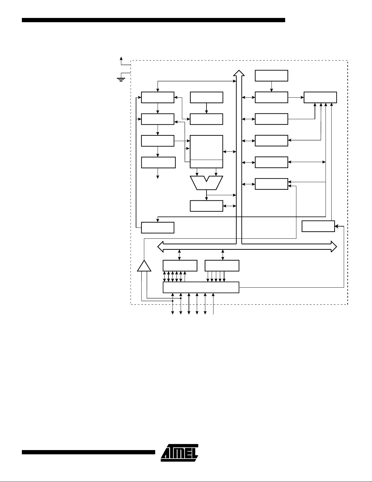
Figure 1. The ATtiny11 Block Diagram
VCC
GND
PROGRAM
COUNTER
STACK
POINTER
8-BIT DATA BUS
INTERNAL
OSCILLATOR
WATCHDOG
TIMER
ATtiny11/12
TIMING AND
CONTROL
PROGRAM
FLASH
INSTRUCTION
REGISTER
INSTRUCTION
DECODER
CONTROL
LINES
PROGRAMMING
LOGIC
-
ANALOG
DATA REGISTER
ARATOR
COMP
+
PORTB
PORTB DRIVERS
HARDWARE
STACK
GENERALPURPOSE
REGISTERS
Z
ALU
STATUS
REGISTER
DATA DIR.
REG. PORTB
MCU CONTROL
REGISTER
MCU STATUS
REGISTER
TIMER/
COUNTER
INTERRUPT
UNIT
OSCILLATORS
1006C–09/01
PB0-PB5
3
Page 4
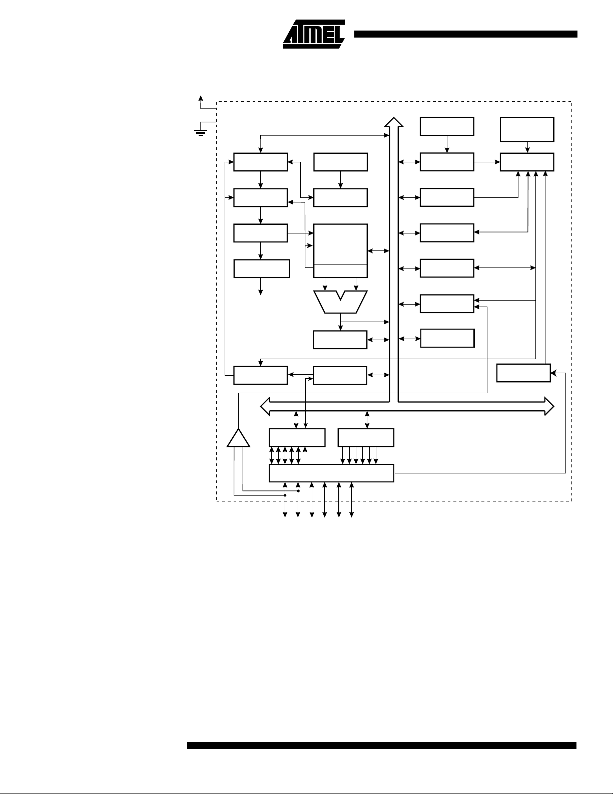
ATtiny12 Block Diagram Figure 2. The ATtiny12 Block Diagram
VCC
GND
PROGRAM
COUNTER
STACK
POINTER
8-BIT DATA BUS
INTERNAL
OSCILLATOR
WATCHDOG
TIMER
INTERNAL
CALIBRATED
OSCILLATOR
TIMING AND
CONTROL
PROGRAM
FLASH
INSTRUCTION
REGISTER
INSTRUCTION
DECODER
CONTROL
LINES
PROGRAMMING
LOGIC
-
ANALOG
DATA REGISTER
ARATOR
COMP
+
PORTB
PORTB DRIVERS
HARDWARE
STACK
GENERALPURPOSE
REGISTERS
Z
ALU
STATUS
REGISTER
SPI
DATA DIR.
REG. PORTB
MCU CONTROL
REGISTER
MCU STATUS
REGISTER
TIMER/
COUNTER
INTERRUPT
UNIT
EEPROM
OSCILLATORS
PB0-PB5
The ATtiny12 provides the following features: 1K bytes of Flash, 64 bytes EEPROM, up
to six general-purpose I/O lines, 32 general-purpose working registers, an 8-bit
timer/counter, internal and external interrupts, programmable Watchdog Timer with
internal oscillator, and two software-selectable power-saving modes. The Idle Mode
stops the CPU while allowing the timer/counters and interrupt system to continue functioning. The Power-down Mode saves the register contents but freezes the oscillator,
disabling all other chip functions until the next interrupt or hardware reset. The wake-up
or interrupt on pin change features enable the ATtiny12 to be highly responsive to external events, still featuring the lowest power consumption while in the power-down modes.
The device is manufactured using Atmel’s high-density nonvolatile memory technology.
By combining an RISC 8-bit CPU with Flash on a monolithic chip, the Atmel ATtiny12 is
a powerful microcontroller that provides a highly-flexible and cost-effective solution to
many embedded control applications.
4
ATtiny11/12
1006C–09/01
Page 5

ATtiny11/12
The ATtiny12 AVR is supported with a full suite of program and system development
tools including: macro assemblers, program debugger/simulators, in-circuit emulators,
and evaluation kits.
Pin Descriptions
VCC Supply voltage pin.
GND Ground pin.
Port B (PB5..PB0) Port B is a 6-bit I/O port. PB4..0 are I/O pins that can provide internal pull-ups (selected
for each bit). On ATtiny11, PB5 is input only. On ATtiny12, PB5 is input or open-drain
output. The port pins are tri-stated when a reset condition becomes active, even if the
clock is not running. The use of pins PB5..3 as input or I/O pins is limited, depending on
reset and clock settings, as shown below.
Table 2. PB5..PB3 Functionality vs. Device Clocking Options
Device Clocking Option PB5 PB4 PB3
External Reset Enabled Used
External Reset Disabled Input
(3)
(1)
/I/O
(4)
(2)
-
--
-
External Crystal - Used Used
External Low-frequency Crystal - Used Used
External Ceramic Resonator - Used Used
External RC Oscillator - I/O
External Clock - I/O Used
Internal RC Oscillator - I/O I/O
Notes: 1. “Used” means the pin is used for reset or clock purposes.
2. “-” means the pin function is unaffected by the option.
3. Input means the pin is a port input pin.
4. On ATtiny11, PB5 is input only. On ATtiny12, PB5 is input or open-drain output.
5. I/O means the pin is a port input/output pin.
(5)
Used
XTAL1 Input to the inverting oscillator amplifier and input to the internal clock operating circuit.
XTAL2 Output from the inverting oscillator amplifier.
RESET
Reset input. An external reset is generated by a low level on the RESET pin. Reset
pulses longer than 50 ns will generate a reset, even if the clock is not running. Shorter
pulses are not guaranteed to generate a reset.
Clock Options The device has the following clock source options, selectable by Flash fuse bits as
shown:
1006C–09/01
Table 3. Device Clocking Options Select
Device Clocking Option ATtiny11 CKSEL2..0 ATtiny12 CKSEL3..0
External Crystal/Ceramic Resonator 111 1111 - 1010
External Low-frequency Crystal 110 1001 - 1000
External RC Oscillator 101 0111 - 0101
5
Page 6
Table 3. Device Clocking Options Select (Continued)
Device Clocking Option ATtiny11 CKSEL2..0 ATtiny12 CKSEL3..0
Internal RC Oscillator 100 0100 - 0010
External Clock 000 0001 - 0000
Reserved Other Options -
Note: “1” means unprogrammed, “0” means programmed.
The various choices for each clocking option give different start-up times as shown in
Table 7 on page 18 and Table 9 on page 20.
Internal RC Oscillator The internal RC oscillator option is an on-chip oscillator running at a fixed frequency of 1
MHz in ATtiny11 and 1.2 MHz in ATtiny12. If selected, the device can operate with no
external components. The device is shipped with this option selected. On ATtiny11, the
Watchdog Oscillator is used as a clock, while ATtiny12 uses a separate calibrated
oscillator.
Crystal Oscillator XTAL1 and XTAL2 are input and output, respectively, of an inverting amplifier which can
be configured for use as an on-chip oscillator, as shown in Figure 3. Either a quartz
crystal or a ceramic resonator may be used. Maximum frequency for crystal and resonators is 4 MHz. Minimum voltage for running on a low-frequency crystal is 2.5V.
Figure 3. Oscillator Connections
MAX 1 HC BUFFER
HC
C2
C1
Note: When using the MCU Oscillator as a clock for an external device, an HC buffer should be
connected as indicated in the figure.
XTAL2
XTAL1
GND
External Clock To drive the device from an external clock source, XTAL1 should be driven as shown in
Figure 4.
Figure 4. External Clock Drive Configuration
PB4 (XTAL2)
EXTERNAL
OSCILLATOR
XTAL1
SIGNAL
GND
6
ATtiny11/12
1006C–09/01
Page 7

ATtiny11/12
External RC Oscillator For timing insensitive applications, the external RC configuration shown in Figure 5 can
be used. For details on how to choose R and C, see Table 29 on page 57. The external
RC oscillator is sensitive to noise from neighboring pins, and to avoid problems, PB5
(RESET
put pin.
Figure 5. External RC Configuration
) should be used as an output or reset pin, and PB4 should be used as an out-
VCC
R
C
PB4 (XTAL2)
XTAL1
GND
1006C–09/01
7
Page 8

Architectural Overview
The fast-access register file concept contains 32 x 8-bit general-purpose working registers with a single-clock-cycle access time. This means that during one single clock
cycle, one ALU (Arithmetic Logic Unit) operation is executed. Two operands are output
from the register file, the operation is executed, and the result is stored back in the register file – in one clock cycle.
Two of the 32 registers can be used as a 16-bit pointer for indirect memory access. This
pointer is called the Z-pointer, and can address the register file and the Flash program
memory.
The ALU supports arithmetic and logic functions between registers or between a constant and a register. Single-register operations are also executed in the ALU. Figure 2
shows the ATtiny11/12 AVR RISC microcontroller architecture. The AVR uses a Harvard architecture concept with separate memories and buses for program and data
memories. The program memory is accessed with a two-stage pipelining. While one
instruction is being executed, the next instruction is pre-fetched from the program memory. This concept enables instructions to be executed in every clock cycle. The program
memory is reprogrammable Flash memory.
With the relative jump and relative call instructions, the whole 512 address space is
directly accessed. All AVR instructions have a single 16-bit word format, meaning that
every program memory address contains a single 16-bit instruction.
During interrupts and subroutine calls, the return address program counter (PC) is
stored on the stack. The stack is a 3-level-deep hardware stack dedicated for subroutines and interrupts.
The I/O memory space contains 64 addresses for CPU peripheral functions as control
registers, timer/counters, and other I/O functions. The memory spaces in the AVR architecture are all linear and regular memory maps.
8
ATtiny11/12
1006C–09/01
Page 9
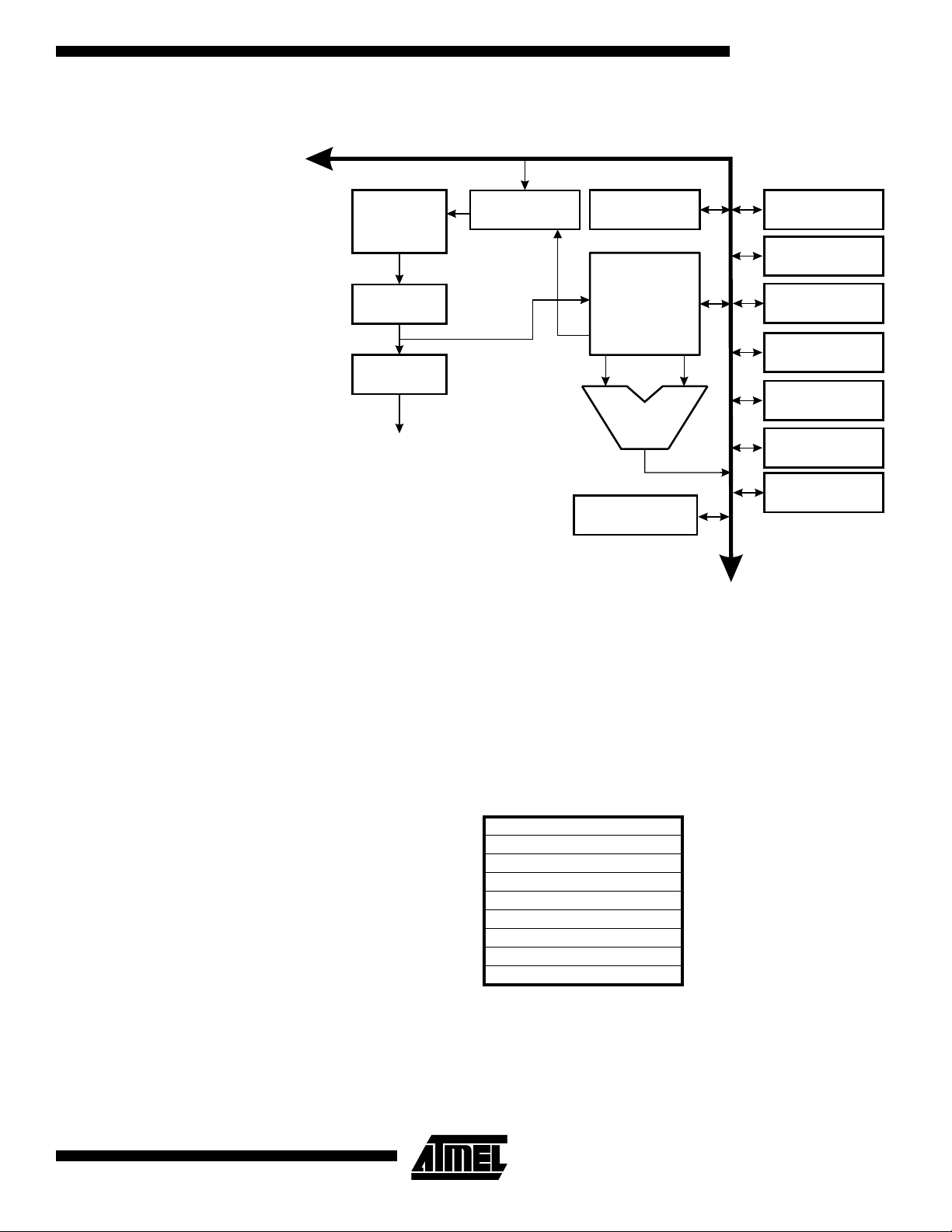
Figure 6. The ATtiny11/12 AVR RISC Architecture
8-bit Data Bus
ATtiny11/12
512 x 16
Program
Flash
Instruction
Register
Instruction
Decoder
Control Lines
Program
Counter
Direct Addressing
Status
and Test
32 x 8
General-
purpose
Registers
ALU
64 x 8 EEPROM
(ATtiny12 only)
Control
Registers
Interrupt
Unit
SPI Unit
(ATtiny12 only)
8-bit
Timer/Counter
Watchdog
Timer
Analog
Comparator
6
I/O Lines
A flexible interrupt module has its control registers in the I/O space with an additional
global interrupt enable bit in the status register. All the different interrupts have a separate interrupt vector in the interrupt vector table at the beginning of the
program memory. The different interrupts have priority in accordance with their interrupt
vector position. The lower the interrupt vector address, the higher the priority.
General-purpose Register File
1006C–09/01
Figure 7 shows the structure of the 32 general-purpose registers in the CPU.
Figure 7. AVR
CPU General-purpose Working Registers
70
R0
R1
R2
General- …
purpose …
Working R28
Registers R29
R30 (Z-register low byte)
R31 (Z-register high byte)
All the register operating instructions in the instruction set have direct- and single-cycle
access to all registers. The only exception is the five constant arithmetic and logic
instructions SBCI, SUBI, CPI, ANDI, and ORI between a constant and a register and the
LDI instruction for load-immediate constant data. These instructions apply to the second
half of the registers in the register file – R16..R31. The general SBC, SUB, CP, AND,
9
Page 10
OR and all other operations between two registers or on a single register apply to the
entire register file.
Registers 30 and 31 form a 16-bit pointer (the Z-pointer) which is used for indirect Flash
memory and register file access. When the register file is accessed, the contents of R31
are discarded by the CPU.
ALU – Arithmetic Logic Unit
The high-performance AVR ALU operates in direct connection with all the 32 generalpurpose working registers. Within a single clock cycle, ALU operations between registers in the register file are executed. The ALU operations are divided into three main
categories – arithmetic, logic and bit-functions. Some microcontrollers in the AVR product family feature a hardware multiplier in the arithmetic part of the ALU.
Flash Program Memory The ATtiny11/12 contains 1K bytes on-chip Flash memory for program storage. Since
all instructions are single 16-bit words, the Flash is organized as 512 x 16 words. The
Flash memory has an endurance of at least 1000 write/erase cycles.
The ATtiny11/12 Program Counter is 9 bits wide, thus addressing the 512 words Flash
program memory.
See page 44 for a detailed description on Flash memory programming.
Program and Data Addressing Modes
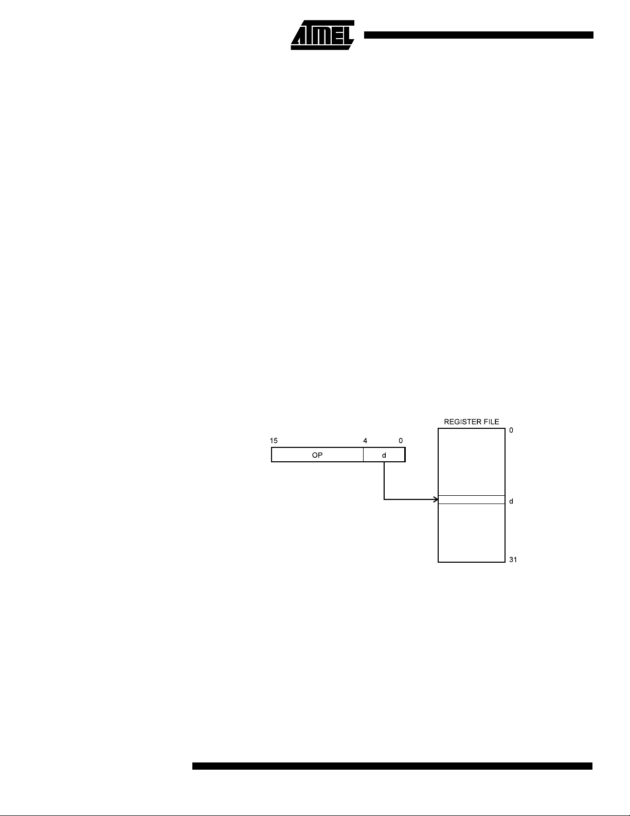
Register Direct, Single Register Rd
The ATtiny11/12 AVR RISC Microcontroller supports powerful and efficient addressing
modes. This section describes the different addressing modes supported in the
ATtiny11/12. In the figures, OP means the operation code part of the instruction word.
To simplify, not all figures show the exact location of the addressing bits.
Figure 8. Direct Single-register Addressing
10
The operand is contained in register d (Rd).
ATtiny11/12
1006C–09/01
Page 11
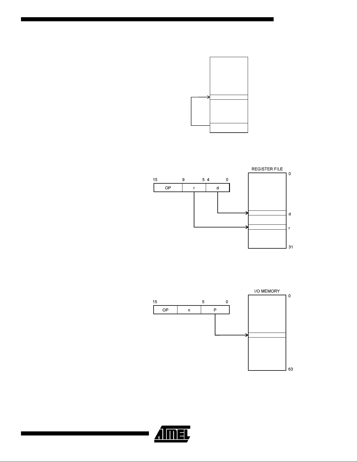
Register Indirect Figure 9. Indirect Register Addressing
ATtiny11/12
REGISTER FILE
0
The register accessed is the one pointed to by the Z-register (R31, R30).
Register Direct, Two Registers
Figure 10. Direct Register Addressing, Two Registers
Rd and Rr
Operands are contained in register r (Rr) and d (Rd). The result is stored in register d
(Rd).
I/O Direct Figure 11. I/O Direct Addressing
Z-register
30
31
1006C–09/01
Operand address is contained in 6 bits of the instruction word. n is the destination or
source register address.
11
Page 12
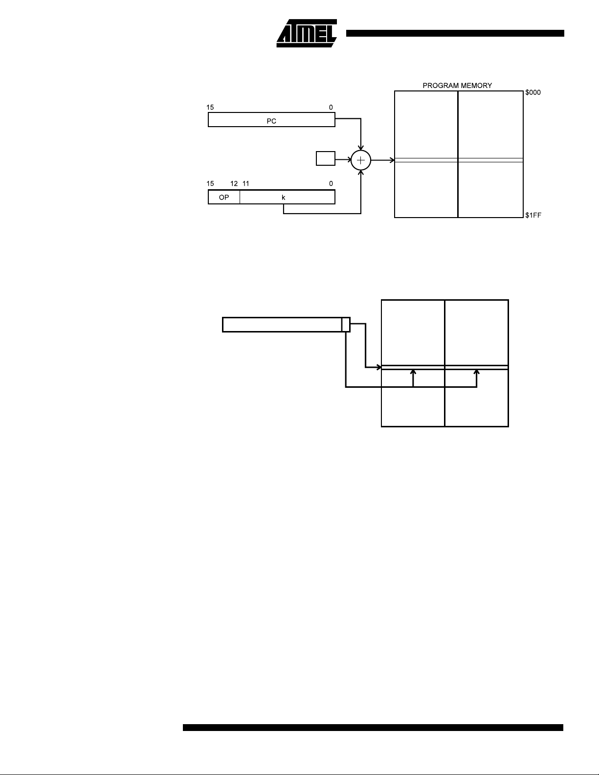
Relative Program Addressing, RJMP and RCALL
Figure 12. Relative Program Memory Addressing
+1
Program execution continues at address PC + k + 1. The relative address k is -2048 to
2047.
Constant Addressing Using the LPM Instruction
Subroutine and Interrupt Hardware Stack
Figure 13. Code Memory Constant Addressing
PROGRAM MEMORY
15 1 0
Z-REGISTER
$000
$1FF
Constant byte address is specified by the Z-register contents. The 15 MSBs select word
address (0 - 511), the LSB selects low byte if cleared (LSB = 0) or high byte if set
(LSB = 1).
The ATtiny11/12 uses a 3-level-deep hardware stack for subroutines and interrupts. The
hardware stack is 9 bits wide and stores the program counter (PC) return address while
subroutines and interrupts are executed.
RCALL instructions and interrupts push the PC return address onto stack level 0, and
the data in the other stack levels 1-2 are pushed one level deeper in the stack. When a
RET or RETI instruction is executed the returning PC is fetched from stack level 0, and
the data in the other stack levels 1-2 are popped one level in the stack.
12
If more than three subsequent subroutine calls or interrupts are executed, the first values written to the stack are overwritten. Pushing four return addresses A1, A2, A3, and
A4, followed by four subroutine or interrupt returns, will pop A4, A3, A2, and once more
A2 from the hardware stack.
ATtiny11/12
1006C–09/01
Page 13
ATtiny11/12
EEPROM Data Memory The ATtiny12 contains 64 bytes of data EEPROM memory. It is organized as a separate
data space, in which single bytes can be read and written. The EEPROM has an endurance of at least 100,000 write/erase cycles. The access between the EEPROM and the
CPU is described on page 36, specifying the EEPROM Address Register, the EEPROM
Data Register, and the EEPROM Control Register.
For SPI data downloading, see “Memory Programming” on page 44 for a detailed
description.
Memory Access and Instruction Execution Timing
This section describes the general access timing concepts for instruction execution and
internal memory access.
The AVR CPU is driven by the System Clock Ø, directly generated from the external
clock crystal for the chip. No internal clock division is used.
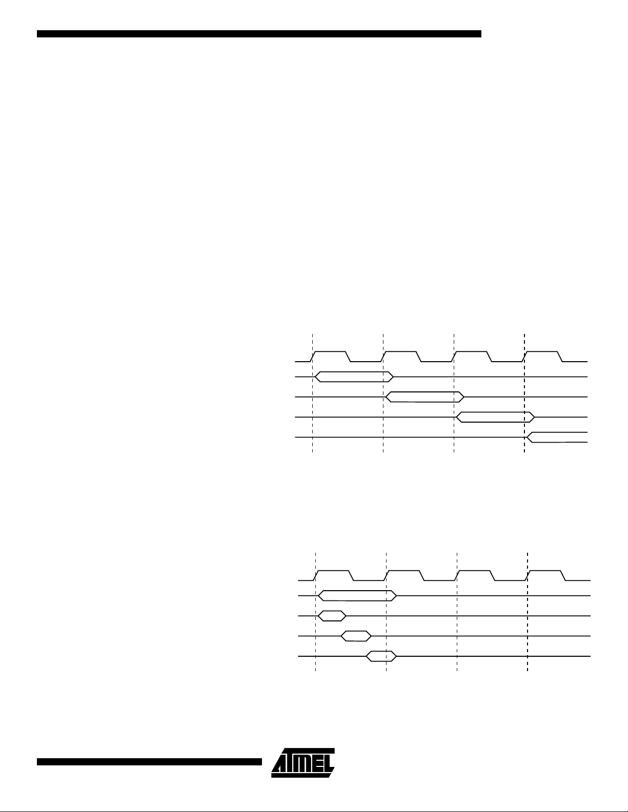
Figure 14 shows the parallel instruction fetches and instruction executions enabled by
the Harvard architecture and the fast-access register file concept. This is the basic pipelining concept to obtain up to 1 MIPS per MHz with the corresponding unique results for
functions per cost, functions per clocks, and functions per power-unit.
Figure 14. The Parallel Instruction Fetches and Instruction Executions
T1 T2 T3 T4
System Clock Ø
1st Instruction Fetch
1st Instruction Execute
2nd Instruction Fetch
2nd Instruction Execute
3rd Instruction Fetch
3rd Instruction Execute
4th Instruction Fetch
Figure 15 shows the internal timing concept for the register file. In a single clock cycle,
an ALU operation using two register operands is executed and the result is stored back
to the destination register.
1006C–09/01
Figure 15. Single-cycle ALU Operation
T1 T2 T3 T4
System Clock Ø
Total Execution Time
Register Operands Fetch
ALU Operation Execute
Result Write Back
13
Page 14

I/O Memory The I/O space definition of the ATtiny11/12 is shown in the following table:
Table 4. ATtiny11/12 I/O Space
Address Hex Name Device Function
$3F SREG ATtiny11/12 Status Register
$3B GIMSK ATtiny11/12 General Interrupt Mask Register
$3A GIFR ATtiny11/12 General Interrupt Flag Register
$39 TIMSK ATtiny11/12 Timer/Counter Interrupt Mask Register
$38 TIFR ATtiny11/12 Timer/Counter Interrupt Flag Register
$35 MCUCR ATtiny11/12 MCU Control Register
$34 MCUSR ATtiny11/12 MCU Status Register
$33 TCCR0 ATtiny11/12 Timer/Counter0 Control Register
$32 TCNT0 ATtiny11/12 Timer/Counter0 (8-bit)
$31 OSCCAL ATtiny12 Oscillator Calibration Register
$21 WDTCR ATtiny11/12 Watchdog Timer Control Register
$1E EEAR ATtiny12 EEPROM Address Register
$1D EEDR ATtiny12 EEPROM Data Register
$1C EECR ATtiny12 EEPROM Control Register
$18 PORTB ATtiny11/12 Data Register, Port B
$17 DDRB ATtiny11/12 Data Direction Register, Port B
$16 PINB ATtiny11/12 Input Pins, Port B
$08 ACSR ATtiny11/12 Analog Comparator Control and Status Register
Note: Reserved and unused locations are not shown in the table.
All the different ATtiny11/12 I/O and peripherals are placed in the I/O space. The different I/O locations are accessed by the IN and OUT instructions transferring data between
the 32 general-purpose working registers and the I/O space. I/O registers within the
address range $00 - $1F are directly bit-accessible using the SBI and CBI instructions.
In these registers, the value of single bits can be checked by using the SBIS and SBIC
instructions. Refer to the Instruction Set Summary for more details.
For compatibility with future devices, reserved bits should be written to zero if accessed.
Reserved I/O memory addressed should never be written.
The different I/O and peripherals control registers are explained in the following
sections.
Status Register – SREG The AVR status register (SREG) at I/O space location $3F is defined as:
Bit 76543210
$3F I T H S V N Z C SREG
Read/Write R/W R/W R/W R/W R/W R/W R/W R/W
Initial Value00000000
• Bit 7 - I: Global Interrupt Enable
14
The global interrupt enable bit must be set (one) for the interrupts to be enabled. The
individual interrupt enable control is then performed in separate control registers. If the
global interrupt enable register is cleared (zero), none of the interrupts are enabled inde-
ATtiny11/12
1006C–09/01
Page 15

ATtiny11/12
pendent of the individual interrupt enable settings. The I-bit is cleared by hardware after
an interrupt has occurred, and is set by the RETI instruction to enable subsequent
interrupts.
• Bit 6 - T: Bit Copy Storage
The bit copy instructions BLD (Bit LoaD) and BST (Bit STore) use the T-bit as source
and destination for the operated bit. A bit from a register in the register file can be copied
into T by the BST instruction, and a bit in T can be copied into a bit in a register in the
register file by the BLD instruction.
• Bit 5 - H: Half Carry Flag
The half carry flag H indicates a half-carry in some arithmetic operations. See the
Instruction Set description for detailed information.
• Bit 4 - S: Sign Bit, S = N
The S-bit is always an exclusive or between the negative flag N and the two’s complement overflow flag V. See the Instruction Set description for detailed information.
• Bit 3 - V: Two’s Complement Overflow Flag
The two’s complement overflow flag V supports two’s complement arithmetic. See the
Instruction Set description for detailed information.
• Bit 2 - N: Negative Flag
⊕ V
Reset and Interrupt Handling
The negative flag N indicates a negative result from an arithmetical or logical operation.
See the Instruction Set description for detailed information.
• Bit 1 - Z: Zero Flag
The zero flag Z indicates a zero result from an arithmetical or logical operation. See the
Instruction Set description for detailed information.
• Bit 0 - C: Carry Flag
The carry flag C indicates a carry in an arithmetical or logical operation. See the Instruction Set description for detailed information.
Note that the status register is not automatically stored when entering an interrupt routine and restored when returning from an interrupt routine. This must be handled by
software.
The ATtiny11 provides four different interrupt sources and the ATtiny12 provides five.
These interrupts and the separate reset vector each have a separate program vector in
the program memory space. All the interrupts are assigned individual enable bits which
must be set (one) together with the I-bit in the status register in order to enable the
interrupt.
The lowest addresses in the program memory space are automatically defined as the
Reset and Interrupt vectors. The complete list of vectors is shown in Table 5. The list
also determines the priority levels of the different interrupts. The lower the address, the
higher the priority level. RESET has the highest priority, and next is INT0 – the External
Interrupt Request 0, etc.
1006C–09/01
15
Page 16

Table 5. Reset and Interrupt Vectors
Vector No. Device Program Address Source Interrupt Definition
External Pin, Power-on
1 ATtiny11 $000 RESET
Reset and Watchdog
Reset
External Pin, Power-on
1 ATtiny12 $000 RESET
Reset, Brown-out Reset
and Watchdog Reset
2 ATtiny11/12 $001 INT0
External Interrupt
Request 0
3 ATtiny11/12 $002 I/O Pins Pin Change Interrupt
4 ATtiny11/12 $003 TIMER0, OVF0
Timer/Counter0
Overflow
5 ATtiny11 $004 ANA_COMP Analog Comparator
5 ATtiny12 $004 EE_RDY EEPROM Ready
6 ATtiny12 $005 ANA_COMP Analog Comparator
The most typical and general program setup for the reset and interrupt vector addresses
for the ATtiny11 are:
Address Labels Code Comments
$000 rjmp RESET ; Reset handler
$001 rjmp EXT_INT0 ; IRQ0 handler
$002 rjmp PIN_CHANGE ; Pin change handler
$003 rjmp TIM0_OVF ; Timer0 overflow handler
$004 rjmp ANA_COMP ; Analog Comparator handler
;
$005 MAIN: <instr> xxx ; Main program start
…… ……
16
The most typical and general program setup for the reset and interrupt vector addresses
for the ATtiny12 are:
Address Labels Code Comments
$000 rjmp RESET ; Reset handler
$001 rjmp EXT_INT0 ; IRQ0 handler
$002 rjmp PIN_CHANGE ; Pin change handler
$003 rjmp TIM0_OVF ; Timer0 overflow handler
$004 rjmp EE_RDY ; EEPROM Ready handler
$005 rjmp ANA_COMP ; Analog Comparator handler
;
$006 MAIN: <instr> xxx ; Main program start
…… ……
ATtiny11/12
1006C–09/01
Page 17
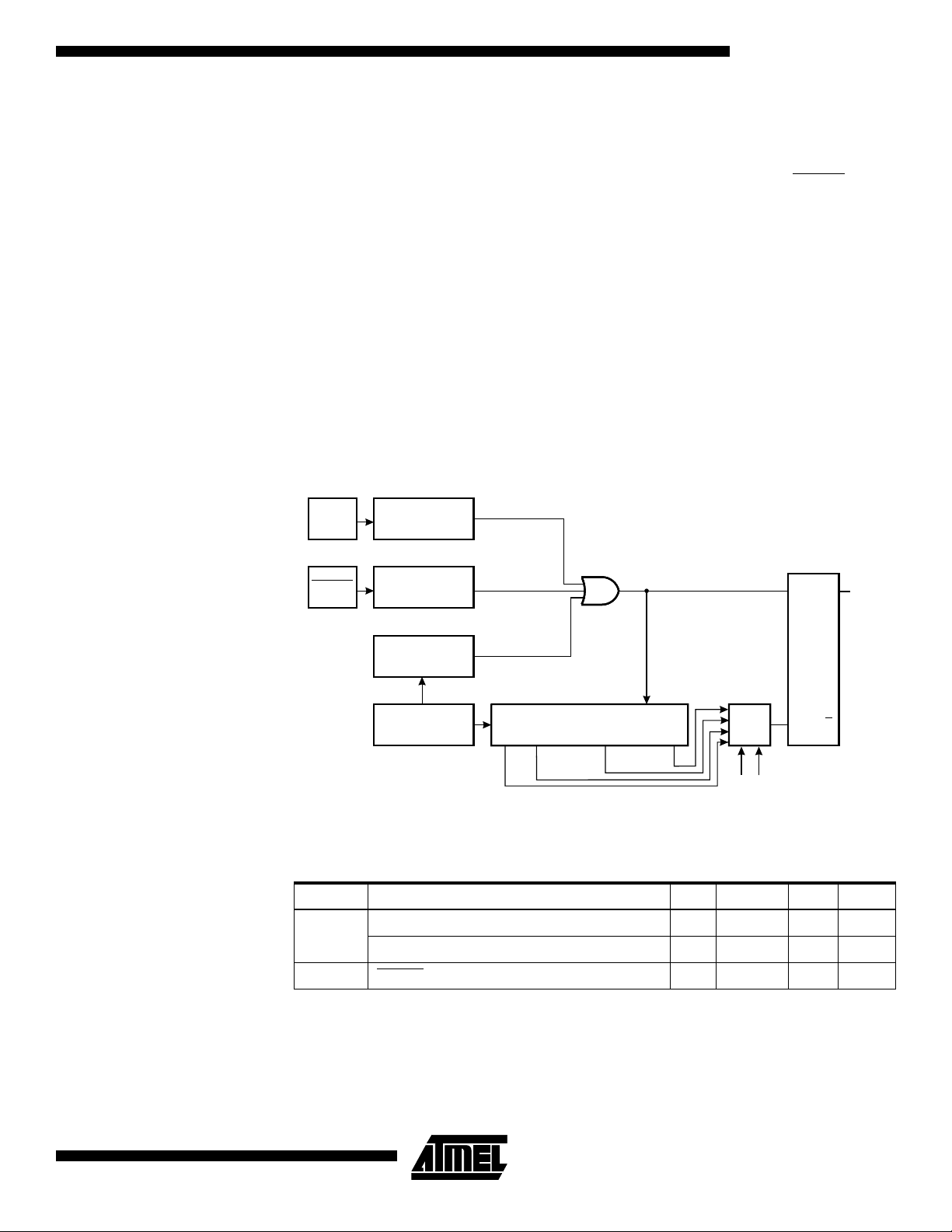
Reset Sources The ATtiny11/12 provides three or four sources of reset:
• Power-on Reset. The MCU is reset when the supply voltage is below the power-on
reset threshold (V
POT
).
• External Reset. The MCU is reset when a low level is present on the RESET pin for
more than 50 ns.
• Watchdog Reset. The MCU is reset when the Watchdog timer period expires and
the Watchdog is enabled.
• Brown-out Reset. The MCU is reset when the supply voltage V
certain voltage (ATtiny12 only).
During reset, all I/O registers are then set to their initial values, and the program starts
execution from address $000. The instruction placed in address $000 must be an RJMP
– relative jump – instruction to the reset handling routine. If the program never enables
an interrupt source, the interrupt vectors are not used, and regular program code can be
placed at these locations. The circuit diagram in Figure 16 shows the reset logic for the
ATtiny11. Figure 17 shows the reset logic for the ATtiny12. Table 6 defines the electrical
parameters of the reset circuitry for ATtiny11. Table 8 shows the parameters of the reset
circuitry for ATtiny12.
Figure 16. Reset Logic for the ATtiny11
VCC
Power-on Reset
Circuit
POR
ATtiny11/12
falls below a
CC
RESET
Reset Circuit
Watchdog
Timer
On-chip
RC Oscillator
COUNTER RESET
20-stage Ripple Counter
Q3 Q19
Q9
Q13
CKSEL
FSTRT
QS
Q
R
Table 6. Reset Characteristics for the ATtiny11
Symbol Parameter Min Typ Max Units
Power-on Reset Threshold Voltage (rising) 1.0 1.4 1.8 V
(1)
V
POT
V
RST
Note: 1. The Power-on Reset will not work unless the supply voltage has been below V
Power-on Reset Threshold Voltage (falling) 0.4 0.6 0.8 V
RESET Pin Threshold Voltage 0.6 V
CC
(falling).
V
INTERNAL
RESET
POT
1006C–09/01
17
Page 18

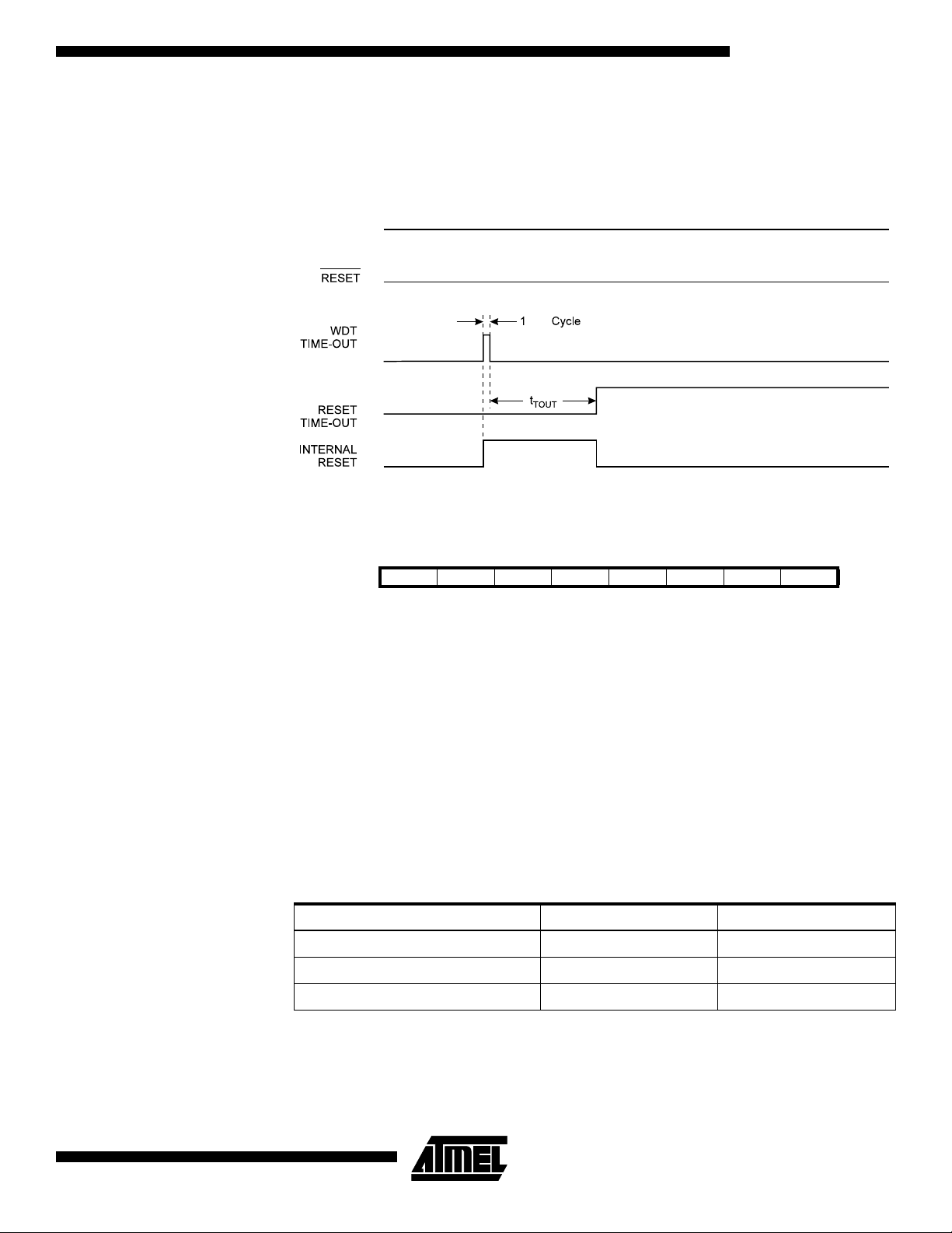
Power-on Reset for the ATt iny 11
A Power-on Reset (POR) circuit ensures that the device is reset from power-on. As
shown in Figure 16, an internal timer is clocked from the watchdog timer. This timer prevents the MCU from starting a certain period after V
Threshold Voltage – V
period – t
. The FSTRT fuse bit in the Flash can be programmed to give a shorter
TOUT
. See Figure 18. The total reset period is the Delay Time-out
POT
has reached the Power-on
CC
start-up time.The start-up times for the different clock options are shown in the following
table. The Watchdog Oscillator is used for timing the start-up time, and this oscillator is
voltage dependent as shown in the section “ATtiny11 Typical Characteristics” on page
58.
Table 7. Start-up Times for the ATtiny11 (V
Selected Clock Option
External Crystal 67 ms 4.2 ms
External Ceramic Resonator 67 ms 4.2 ms
External Low-frequency Crystal 4.2 s 4.2 s
External RC Oscillator 4.2 ms 67 µs
Internal RC Oscillator 4.2 ms 67 µs
External Clock 4.2 ms
FSTRT Unprogrammed FSTRT Programmed
If the built-in start-up delay is sufficient, RESET
an external pull-up resistor. By holding the RESET
= 2.7V)
CC
Start-up Time t
TOUT
5 clocks from reset,
2 clocks from power-down
can be connected to VCC directly or via
pin low for a period after VCC has
been applied, the Power-on Reset period can be extended. Refer to Figure 19 for a timing example on this.
18
ATtiny11/12
1006C–09/01
Page 19
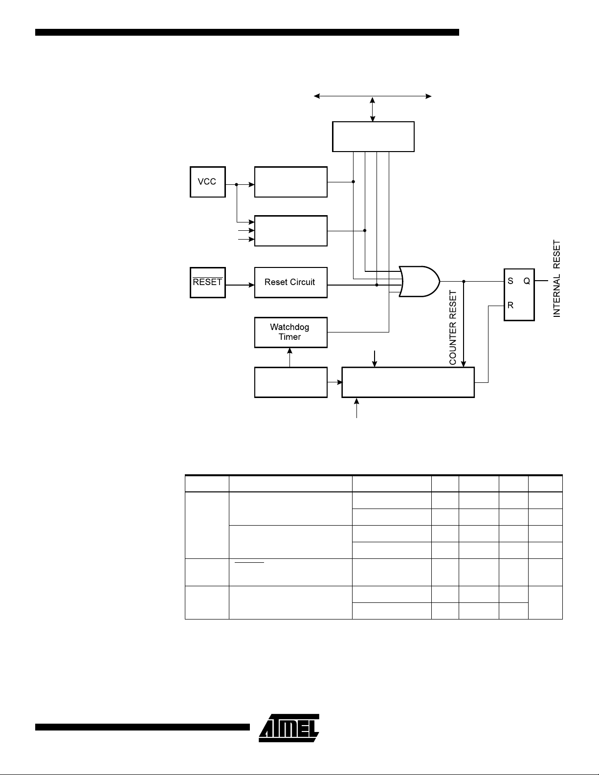
Figure 17. Reset Logic for the ATtiny12
DATA BUS
MCU Status
Register (MCUSR)
Power-on Reset
Circuit
PORF
BORF
EXTRF
ATtiny11/12
WDRF
BODEN
BODLEVEL
Brown-out
Reset Circuit
CKSEL[3:0]
On-chip
RC Oscillator
Delay Counters
Full
CK
Table 8. Reset Characteristics for the ATtiny12
Symbol Parameter Condition Min Typ Max Units
Power-on Reset Threshold
Voltage (rising)
(1)
V
POT
Power-on Reset Threshold
Voltage (falling)
V
RST
RESET Pin Threshold
Volt age
BOD disabled 1.0 1.4 1.8 V
BOD enabled 0.6 1.2 1.8 V
BOD disabled 0.4 0.6 0.8 V
BOD enabled 0.6 1.2 1.8 V
0.6V
CC
V
1006C–09/01
V
BOT
Brown-out Reset Threshold
Volt age
(BODLEVEL = 1) 1.5 1.8 1.9
V
(BODLEVEL = 0) 2.6 2.7 2.8
Note: 1. The Power-on Reset will not work unless the supply voltage has been below V
(falling).
POT
19
Page 20

Table 9. ATtiny12 Clock Options and Start-up Times
Start-up Time,
V
= 1.8V,
CC
BODLEVEL
CKSEL3..0 Clock Source
1111 Ext. Crystal/Ceramic Resonator
1110 Ext. Crystal/Ceramic Resonator
1101 Ext. Crystal/Ceramic Resonator
1100 Ext. Crystal/Ceramic Resonator 16K CK 16K CK
1011 Ext. Crystal/Ceramic Resonator 3.6 ms + 16K CK 4.2 ms + 16K CK
1010 Ext. Crystal/Ceramic Resonator 57 ms + 16K CK 67 ms + 16K CK
1001 Ext. Low-frequency Crystal 57 ms + 1K CK 67 ms + 1K CK
1000 Ext. Low-frequency Crystal 57 ms + 32K CK 67 ms + 32K CK
0111 Ext. RC Oscillator 6 CK 6 CK
0110 Ext. RC Oscillator 3.6 ms + 6 CK 4.2 ms + 6 CK
0101 Ext. RC Oscillator 57 ms + 6 CK 67 ms + 6 CK
0100 Int. RC Oscillator 6 CK 6 CK
0011 Int. RC Oscillator 3.6 ms + 6 CK 4.2 ms + 6 CK
0010 Int. RC Oscillator 57 ms + 6 CK 67 ms + 6 CK
0001 Ext. Clock 6 CK 6 CK
0000 Ext. Clock 3.6 ms + 6 CK 4.2 ms + 6 CK
Unprogrammed
(1)
1K CK 1K CK
(1)
3.6 ms + 1K CK 4.2 ms + 1K CK
(1)
57 ms 1K CK 67 ms + 1K CK
Start-up Time,
VCC = 2.7V,
BODLEVEL
Programmed
Note: 1. Due to the limited number of clock cycles in the start-up period, it is recommended
that Ceramic Resonator be used.
This table shows the start-up times from reset. From sleep, only the clock counting part
of the start-up time is used. The Watchdog oscillator is used for timing the real-time part
of the start-up time. The number of WDT oscillator cycles used for each time-out is
shown in Table 10.
Table 10. Number of Watchdog Oscillator Cycles
BODLEVEL Time-out Number of Cycles
Unprogrammed 3.6 ms (at Vcc = 1.8V) 256
Unprogrammed 57 ms (at V
Programmed 4.2 ms (at V
Programmed 67 ms (at Vcc = 2.7V) 16K
= 1.8V) 4K
cc
= 2.7V) 1K
cc
The frequency of the watchdog oscillator is voltage dependent as shown in the section
“ATtiny11 Typical Characteristics” on page 58.
Note that the BODLEVEL fuse can be used to select start-up times even if the Brownout Detection is disabled (by leaving the BODEN fuse unprogrammed).
The device is shipped with CKSEL3..0 = 0010.
20
ATtiny11/12
1006C–09/01
Page 21
ATtiny11/12
Power-on Reset for the ATt iny 12
A Power-on Reset (POR) pulse is generated by an on-chip detection circuit. The detection level is nominally 1.4V. The POR is activated whenever V
is below the detection
CC
level. The POR circuit can be used to trigger the start-up reset, as well as detect a failure in supply voltage.
The Power-on Reset (POR) circuit ensures that the device is reset from power-on.
Reaching the Power-on Reset threshold voltage invokes a delay counter, which determines the delay for which the device is kept in Reset after V
rise. The time-out period
CC
of the delay counter can be defined by the user through the CKSEL fuses. The different
selections for the delay period are presented in Table 9. The Reset signal is activated
again, without any delay, when the V
If the built-in start-up delay is sufficient, RESET
an external pull-up resistor. See Figure 18. By holding the RESET
after V
has been applied, the Power-on Reset period can be extended. Refer to Fig-
CC
decreases below detection level.
CC
can be connected to VCC directly or via
pin low for a period
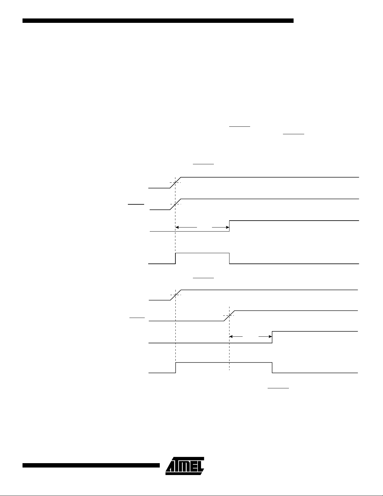
ure 19 for a timing example on this.
t
TOUT
Tied to VCC.
Figure 18. MCU Start-up, RESET
V
V
CC
RESET
TIME-OUT
POT
V
RST
INTERNAL
RESET
Figure 19. MCU Start-up, RESET
V
V
RESET
TIME-OUT
INTERNAL
RESET
CC
POT
Extended Externally
V
RST
t
TOUT
External Reset An external reset is generated by a low level on the RESET
than 50 ns will generate a reset, even if the clock is not running. Shorter pulses are not
guaranteed to generate a reset. When the applied signal reaches the Reset Threshold
Voltage – V
period (t
– on its positive edge, the delay timer starts the MCU after the Time-out
RST
) has expired.
TOUT
pin. Reset pulses longer
1006C–09/01
21
Page 22
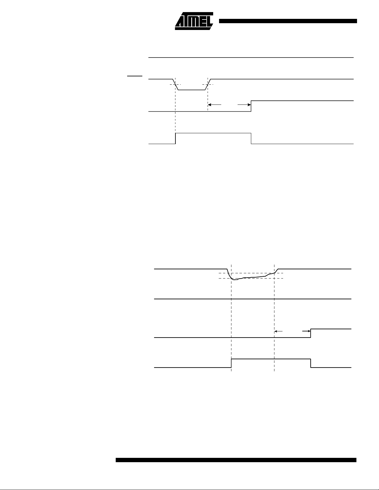
Figure 20. External Reset during Operation
V
CC
Brown-out Detection (ATtiny12)
RESET
TIME-OUT
INTERNAL
RESET
ATtiny12 has an on-chip brown-out detection (BOD) circuit for monitoring the V
V
RST
t
TOUT
level
CC
during the operation. The BOD circuit can be enabled/disabled by the fuse BODEN.
When BODEN is enabled (BODEN programmed), and V
level, the brown-out reset is immediately activated. When V
decreases below the trigger
CC
increases above the trig-
CC
ger level, the brown-out reset is deactivated after a delay. The delay is defined by the
user in the same way as the delay of POR signal, in Table 5. The trigger level for the
BOD can be selected by the fuse BODLEVEL to be 1.8V (BODLEVEL unprogrammed),
or 2.7V (BODLEVEL programmed). The trigger level has a hysteresis of 50 mV to
ensure spike-free brown-out detection.
The BOD circuit will only detect a drop in V
if the voltage stays below the trigger level
CC
for longer than 7 µs for trigger level 2.7V, 24 µs for trigger level 1.8V (typical values).
Figure 21. Brown-out Reset during Operation (ATtiny12)
V
CC
RESET
TIME-OUT
INTERNAL
RESET
Note: The hysteresis on V
BOT
: V
V
BOT-
BOT +
= V
+ 25 mV, V
BOT
BOT-
= V
V
BOT
BOT+
t
TOUT
- 25 mV.
22
ATtiny11/12
1006C–09/01
Page 23
ATtiny11/12
Watchdog Reset When the Watchdog times out, it will generate a short reset pulse of 1 CK cycle dura-
tion. On the falling edge of this pulse, the delay timer starts counting the Time-out period
). Refer to page 34 for details on operation of the Watchdog.
(t
TOUT
Figure 22. Watchdog Reset during Operation
V
CC
CK
MCU Status Register – MCUSR of the ATtiny11
The MCU Status Register provides information on which reset source caused an MCU
reset.
Bit 76543210
$34 ------EXTRFPORFMCUSR
Read/WriteRRRRRRR/WR/W
Initial Value000000See bit description
• Bit 7..2 - Res: Reserved Bits
These bits are reserved bits in the ATtiny11 and always read as zero.
• Bit 1 - EXTRF: EXTernal Reset Flag
After a power-on reset, this bit is undefined (X). It will be set by an external reset. A
watchdog reset will leave this bit unchanged.
• Bit 0 - PORF: Power-on Reset Flag
This bit is set by a power-on reset. A watchdog reset or an external reset will leave this
bit unchanged.
To summarize, the following table shows the value of these two bits after the three
modes of reset.
Table 11. PORF and EXTRF Values after Reset
Reset Source EXTRF PORF
Power-on Undefined 1
1006C–09/01
External Reset 1 Unchanged
Watchdog Reset Unchanged Unchanged
To identify a reset condition, the user software should clear both the PORF and EXTRF
bits as early as possible in the program. Checking the PORF and EXTRF values is done
before the bits are cleared. If the bit is cleared before an external or watchdog reset
occurs, the source of reset can be found by using the following truth table:
23
Page 24

Table 12. Reset Source Identification
EXTRF PORF Reset Source
0 0 Watchdog Reset
1 0 External Reset
0 1 Power-on Reset
1 1 Power-on Reset
MCU Status Register – MCUSR for the ATtiny12
The MCU Status Register provides information on which reset source caused an MCU
reset.
Bit 76543210
$34 ----WDRFBORFEXTRFPORFMCUSR
Read/Write R R R R R/W R/W R/W R/W
Initial Value 0 0 0 0 See Bit Description
• Bit 7..4 - Res: Reserved Bits
These bits are reserved bits in the ATtiny12 and always read as zero.
• Bit 3 - WDRF: Watchdog Reset Flag
This bit is set if a watchdog reset occurs. The bit is reset by a power-on reset, or by writing a logic zero to the flag.
• Bit 2 - BORF: Brown-out Reset Flag
This bit is set if a brown-out reset occurs. The bit is reset by a power-on reset, or by writing a logic zero to the flag.
• Bit 1 - EXTRF: EXTernal Reset Flag
This bit is set if an external reset occurs. The bit is reset by a power-on reset, or by writing a logic zero to the flag.
• Bit 0 - PORF: Power-on Reset Flag
This bit is set if a power-on reset occurs. The bit is reset by writing a logic zero to the
flag.
ATtiny12 Internal Voltage Reference
Voltage Reference Enable Signals and Start-up Time
24
ATtiny11/12
To use the reset flags to identify a reset condition, the user should read and then reset
the MCUSR as early as possible in the program. If the register is cleared before another
reset occurs, the source of the reset can be found by examining the reset flags.
ATtiny12 features an internal voltage reference with a nominal voltage of 1.22V. This
reference is used for Brown-out Detection, and it can be used as an input to the Analog
Comparator.
The voltage reference has a start-up time that may influence the way it should be used.
The maximum start-up time is 10µs. To save power, the reference is not always turned
on. The reference is on during the following situations:
1. When BOD is enabled (by programming the BODEN fuse)
2. When the bandgap reference is connected to the Analog Comparator (by setting
the AINBG bit in ACSR)
Thus, when BOD is not enabled, after setting the AINBG bit, the user must always allow
the reference to start up before the output from the Analog Comparator is used. The
1006C–09/01
Page 25

ATtiny11/12
bandgap reference uses approximately 10 µA, and to reduce power consumption in
Power-down mode, the user can turn off the reference when entering this mode.
Interrupt Handling The ATtiny11/12 has two 8-bit Interrupt Mask control registers; GIMSK – General Inter-
rupt Mask register and TIMSK – Timer/Counter Interrupt Mask register.
When an interrupt occurs, the Global Interrupt Enable I-bit is cleared (zero) and all interrupts are disabled. The user software can set (one) the I-bit to enable nested interrupts.
The I-bit is set (one) when a Return from Interrupt instruction – RETI – is executed.
When the Program Counter is vectored to the actual interrupt vector in order to execute
the interrupt handling routine, hardware clears the corresponding flag that generated the
interrupt. Some of the interrupt flags can also be cleared by writing a logic one to the flag
bit position(s) to be cleared.
If an interrupt condition occurs when the corresponding interrupt enable bit is cleared
(zero), the interrupt flag will be set and remembered until the interrupt is enabled, or the
flag is cleared by software.
If one or more interrupt conditions occur when the global interrupt enable bit is cleared
(zero), the corresponding interrupt flag(s) will be set and remembered until the global
interrupt enable bit is set (one), and will be executed by order of priority.
Note that external level interrupt does not have a flag, and will only be remembered for
as long as the interrupt condition is active.
Note that the status register is not automatically stored when entering an interrupt routine and restored when returning from an interrupt routine. This must be handled by
software.
Interrupt Response Time The interrupt execution response for all the enabled AVR interrupts is 4 clock cycles
minimum. After the 4 clock cycles, the program vector address for the actual interrupt
handling routine is executed. During this 4-clock-cycle period, the Program Counter (9
bits) is pushed onto the Stack. The vector is normally a relative jump to the interrupt routine, and this jump takes 2 clock cycles. If an interrupt occurs during execution of a
multi-cycle instruction, this instruction is completed before the interrupt is served. In
ATtiny12, if an interrupt occurs when the MCU is in Sleep mode, the interrupt response
time is increased by 4 clock cycles.
A return from an interrupt handling routine takes 4 clock cycles. During these 4 clock
cycles, the Program Counter (9 bits) is popped back from the Stack, and the I-flag in
SREG is set. When AVR exits from an interrupt, it will always return to the main program
and execute one more instruction before any pending interrupt is served.
General Interrupt Mask Register – GIMSK
Bit 7 6 5 4 3 2 1 0
$3B - INT0 PCIE - - - - - GIMSK
Read/Write R R/W R/W R R R R R
Initial Value 0 0 0 0 0 0 0 0
1006C–09/01
• Bit 7 - Res: Reserved Bit
This bit is a reserved bit in the ATtiny11/12 and always reads as zero.
• Bit 6 - INT0: External Interrupt Request 0 Enable
When the INT0 bit is set (one) and the I-bit in the Status Register (SREG) is set (one),
the external pin interrupt is enabled. The Interrupt Sense Control0 bits 1/0 (ISC01 and
ISC00) in the MCU general Control Register (MCUCR) define whether the external
25
Page 26

General Interrupt Flag Register – GIFR
interrupt is activated on rising or falling edge, on pin change, or low level of the INT0 pin.
Activity on the pin will cause an interrupt request even if INT0 is configured as an output.
The corresponding interrupt of External Interrupt Request 0 is executed from program
memory address $001. See also “External Interrupts.”
• Bit 5 - PCIE: Pin Change Interrupt Enable
When the PCIE bit is set (one) and the I-bit in the Status Register (SREG) is set (one),
the interrupt on pin change is enabled. Any change on any input or I/O pin will cause an
interrupt. The corresponding interrupt of Pin Change Interrupt Request is executed from
program memory address $002. See also “Pin Change Interrupt.”
• Bits 4..0 - Res: Reserved Bits
These bits are reserved bits in the ATtiny11/12 and always read as zero.
Bit 7 6 5 4 3 2 1 0
$3A - INTF0 PCIF - - - - - GIFR
Read/Write R R/W R/W R R R R R
Initial Value 0 0 0 0 0 0 0 0
• Bit 7 - Res: Reserved Bit
This bit is a reserved bit in the ATtiny11/12 and always reads as zero.
• Bit 6 - INTF0: External Interrupt Flag0
When an edge on the INT0 pin triggers an interrupt request, the corresponding interrupt
flag, INTF0 becomes set (one). If the I-bit in SREG and the corresponding interrupt
enable bit, INT0 bit in GIMSK, are set (one), the MCU will jump to the interrupt vector.
The flag is cleared when the interrupt routine is executed. Alternatively, the flag can be
cleared by writing a logical one to it. The flag is always cleared when INT0 is configured
as level interrupt.
• Bit 5 - PCIF: Pin Change Interrupt Flag
Timer/Counter Interrupt Mask Register – TIMSK
When an event on any input or I/O pin triggers an interrupt request, PCIF becomes set
(one). If the I-bit in SREG and the PCIE bit in GIMSK are set (one), the MCU will jump to
the interrupt vector at address $002. The flag is cleared when the interrupt routine is
executed. Alternatively, the flag can be cleared by writing a logical one to it.
• Bits 4..0 - Res: Reserved Bits
These bits are reserved bits in the ATtiny11/12 and always read as zero.
Bit 7 6 5 4 3 2 1 0
$39 - - - - - - TOIE0 - TIMSK
Read/Write R R R R R R R/W R
Initial Value 0 0 0 0 0 0 0 0
• Bit 7..2 - Res: Reserved Bits
These bits are reserved bits in the ATtiny11/12 and always read as zero.
• Bit 1 - TOIE0: Timer/Counter0 Overflow Interrupt Enable
When the TOIE0 bit is set (one) and the I-bit in the Status Register is set (one), the
Timer/Counter0 Overflow interrupt is enabled. The corresponding interrupt (at vector
$003) is executed if an overflow in Timer/Counter0 occurs, i.e., when the Overflow Flag
(Timer0) is set (one) in the Timer/Counter Interrupt Flag Register – TIFR.
26
ATtiny11/12
1006C–09/01
Page 27

Timer/Counter Interrupt Flag Register – TIFR
ATtiny11/12
• Bit 0 - Res: Reserved Bit
This bit is a reserved bit in the ATtiny11/12 and always reads as zero.
Bit 7 6 5 4 3 2 1 0
$38 -- ----TOV0-TIFR
Read/Write R R R R R R R/W R
Initial Value 0 0 0 0 0 0 0 0
• Bits 7..2 - Res: Reserved Bits
These bits are reserved bits in the ATtiny11/12 and always read as zero.
• Bit 1 - TOV0: Timer/Counter0 Overflow Flag
The bit TOV0 is set (one) when an overflow occurs in Timer/Counter0. TOV0 is cleared
by hardware when executing the corresponding interrupt handling vector. Alternatively,
TOV0 is cleared by writing a logical one to the flag. When the SREG I-bit, TOIE0
(Timer/Counter0 Overflow Interrupt Enable), and TOV0 are set (one), the
Timer/Counter0 Overflow interrupt is executed.
• Bit 0 - Res: Reserved bit
This bit is a reserved bit in the ATtiny11/12 and always reads as zero.
External Interrupt The external interrupt is triggered by the INT0 pin. Observe that, if enabled, the interrupt
will trigger even if the INT0 pin is configured as an output. This feature provides a way of
generating a software interrupt. The external interrupt can be triggered by a falling or rising edge, a pin change, or a low level. This is set up as indicated in the specification for
the MCU Control Register – MCUCR. When the external interrupt is enabled and is configured as level triggered, the interrupt will trigger as long as the pin is held low.
The external interrupt is set up as described in the specification for the MCU Control
Register – MCUCR.
Pin Change Interrupt The pin change interrupt is triggered by any change on any input or I/O pin. Change on
pins PB2..0 will always cause an interrupt. Change on pins PB5..3 will cause an interrupt if the pin is configured as input or I/O, as described in the section “Pin Descriptions”
on page 5. Observe that, if enabled, the interrupt will trigger even if the changing pin is
configured as an output. This feature provides a way of generating a software interrupt.
Also observe that the pin change interrupt will trigger even if the pin activity triggers
another interrupt, for example, the external interrupt. This implies that one external
event might cause several interrupts.
The values on the pins are sampled before detecting edges. If pin change interrupt is
enabled, pulses that last longer than one CPU clock period will generate an interrupt.
Shorter pulses are not guaranteed to generate an interrupt.
1006C–09/01
27
Page 28

MCU Control Register – MCUCR
The MCU Control Register contains control bits for general MCU functions.
Bit 76543210
$35 - (PUD) SE SM - - ISC01 ISC00 MCUCR
Read/Write R R(/W) R/W R/W R R R/W R/W
Initial Value 0 0 0 0 0 0 0 0
Note: The Pull-up Disable (PUD) bit is only available in ATtiny12.
• Bit 7 - Res: Reserved Bit
This bit is a reserved bit in the ATtiny11/12 and always reads as zero.
• Bit 6 - Res: Reserved Bit in ATtiny11
This bit is a reserved bit in the ATtiny11 and always reads as zero.
• Bit 6 - PUD: Pull-up Disable in ATtiny12
Setting this bit, disables all pull-ups on port B. If this bit is cleared, the pull-ups can be
individually enabled as described in section “I/O Port B” on page 41.
• Bit 5 - SE: Sleep Enable
The SE bit must be set (one) to make the MCU enter the Sleep Mode when the SLEEP
instruction is executed. To avoid the MCU entering the Sleep Mode unless it is the programmer’s purpose, it is recommended to set the Sleep Enable SE bit just before the
execution of the SLEEP instruction.
• Bit 4 - SM: Sleep Mode
This bit selects between the two available sleep modes. When SM is cleared (zero), Idle
Mode is selected as Sleep Mode. When SM is set (one), Power-down Mode is selected
as Sleep Mode. For details, refer to the paragraph “Sleep Modes” below.
• Bits 3, 2 - Res: Reserved Bits
These bits are reserved bits in the ATtiny11/12 and always read as zero.
• Bits 1, 0 - ISC01, ISC00: Interrupt Sense Control0 Bit 1 and Bit 0
The External Interrupt 0 is activated by the external pin INT0 if the SREG I-flag and the
corresponding interrupt mask are set. The following table shows how to set the ISC bits
to generate an external interrupt:
Table 13. Interrupt 0 Sense Control
ISC01 ISC00 Description
0 0 The low level of INT0 generates an interrupt request.
0 1 Any change on INT0 generates an interrupt request
1 0 The falling edge of INT0 generates an interrupt request.
1 1 The rising edge of INT0 generates an interrupt request.
The value on the INT0 pin is sampled before detecting edges. If edge interrupt is
selected, pulses that last longer than one CPU clock period will generate an interrupt.
Shorter pulses are not guaranteed to generate an interrupt. If low-level interrupt is
selected, the low level must be held until the completion of the currently executing
instruction to generate an interrupt. If enabled, a level-triggered interrupt will generate
an interrupt request as long as the pin is held low.
28
ATtiny11/12
1006C–09/01
Page 29

ATtiny11/12
Sleep Modes for the ATtiny 11
Idle Mode When the SM bit is cleared (zero), the SLEEP instruction forces the MCU into the Idle
Power-down Mode When the SM bit is set (one), the SLEEP instruction forces the MCU into the Power-
To enter the sleep modes, the SE bit in MCUCR must be set (one) and a SLEEP instruction must be executed. The SM bit in the MCUCR register selects which sleep mode
(Idle or Power-down) will be activated by the SLEEP instruction. If an enabled interrupt
occurs while the MCU is in a sleep mode, the MCU awakes, executes the interrupt routine, and resumes execution from the instruction following SLEEP. On wake-up from
Power Down Mode on pin change, two instruction cycles are executed before the pin
change interrupt flag is updated. During these cycles, the prosessor executes intructions, but the interrupt condition is not readable, and the interrupt routine has not startet
yet. The contents of the register file and I/O memory are unaltered. If a reset occurs during Sleep Mode, the MCU wakes up and executes from the Reset vector.
Mode, stopping the CPU but allowing Timer/Counters, Watchdog and the interrupt system to continue operating. This enables the MCU to wake up from external triggered
interrupts as well as internal ones like Timer Overflow interrupt and Watchdog Reset. If
wake-up from the Analog Comparator interrupt is not required, the analog comparator
can be powered down by setting the ACD-bit in the Analog Comparator Control and Status register – ACSR. This will reduce power consumption in Idle Mode. When the MCU
wakes up from Idle mode, the CPU starts program execution immediately.
down Mode. In this mode, the external oscillator is stopped, while the external interrupts
and the Watchdog (if enabled) continue operating. Only an external reset, a watchdog
reset (if enabled), an external level interrupt, or an pin change interrupt can wake up the
MCU.
Note that if a level-triggered or pin change interrupt is used for wake-up from powerdown, the changed level must be held for a time longer than the reset delay period of
. Otherwise, the MCU will fail to wake up.
t
TOUT
Sleep Modes for the ATtiny 12
Idle Mode When the SM bit is cleared (zero), the SLEEP instruction forces the MCU into the Idle
Power-down Mode When the SM bit is set (one), the SLEEP instruction forces the MCU into the Power-
To enter the sleep modes, the SE bit in MCUCR must be set (one) and a SLEEP instruction must be executed. The SM bit in the MCUCR register selects which sleep mode
(Idle or Power-down) will be activated by the SLEEP instruction. If an enabled interrupt
occurs while the MCU is in a sleep mode, the MCU awakes. The CPU is then halted for
four cycles, it executes the interrupt routine, and resumes execution from the instruction
following SLEEP. The contents of the register file and I/O memory are unaltered. If a
reset occurs during sleep mode, the MCU wakes up and executes from the Reset
vector.
Mode stopping the CPU but allowing Timer/Counters, Watchdog and the interrupt system to continue operating. This enables the MCU to wake up from external triggered
interrupts as well as internal ones like Timer Overflow interrupt and Watchdog Reset. If
wake-up from the Analog Comparator interrupt is not required, the analog comparator
can be powered down by setting the ACD-bit in the Analog Comparator Control and Status Register – ACSR. This will reduce power consumption in Idle Mode.
down Mode. In this mode, the external oscillator is stopped, while the external interrupts
and the Watchdog (if enabled) continue operating. Only an external reset, a watchdog
reset (if enabled), an external level interrupt, or a pin change interrupt can wake up the
MCU.
1006C–09/01
29
Page 30

Note that if a level triggered or pin change interrupt is used for wake-up from Powerdown Mode, the changed level must be held for a time to wake up the MCU. This makes
the MCU less sensitive to noise. The wake-up period is equal to the clock-counting part
of the reset period (See Table 9). The MCU will wake up from the power-down if the
input has the required level for two watchdog oscillator cycles. If the wake-up period is
shorter than two watchdog oscillator cycles, the MCU will wake up if the input has the
required level for the duration of the wake-up period. If the wake-up condition disappears before the wake-up period has expired, the MCU will wake up from power-down
without executing the corresponding interrupt. The period of the watchdog oscillator is
2.7 µs (nominal) at 3.0V and 25
°C. The frequency of the watchdog oscillator is voltage
dependent as shown in the section “ATtiny11 Typical Characteristics” on page 58.
When waking up from Power-down Mode, there is a delay from the wake-up condition
occurs until the wake-up becomes effective. This allows the clock to restart and become
stable after having been stopped. The wake-up period is defined by the same CKSEL
fuses that define the reset time-out period.
ATtiny12 Calibrated Internal RC Oscillator
Oscillator Calibration Register – OSCCAL
In ATtiny12, the calibrated internal oscillator provides a fixed 1.2 MHz (nominal) clock at
5V and 25
°C. This clock may be used as the system clock. See the section “Clock
Options” on page 5 for information on how to select this clock as the system clock. This
oscillator can be calibrated by writing the calibration byte to the OSCCAL register. When
this oscillator is used as the chip clock, the Watchdog Oscillator will still be used for the
Watchdog Timer and for the reset time-out. For details on how to use the pre-programmed calibration value, see the section “Calibration Byte in ATtiny12” on page 45. At
o
5V and 25
C, the pre-programmed calibration byte gives a frequency within ± 1% of the
nominal frequency.
Bit 76543210
$31 CAL7 CAL6 CAL5 CAL4 CAL3 CAL2 CAL1 CAL0 OSCCAL
Read/Write R/W R/W R/W R/W R/W R/W R/W R/W
Initial Value 0 0 0 0 0 0 0 0
• Bits 7..0 - CAL7..0: Oscillator Calibration Value
Writing the calibration byte to this address will trim the internal oscillator to remove process variations from the oscillator frequency. When OSCCAL is zero, the lowest
available frequency is chosen. Writing non-zero values to this register will increase the
frequency of the internal oscillator. Writing $FF to the register gives the highest available
frequency. The calibrated oscillator is used to time EEPROM access. If EEPROM is
written, do not calibrate to more than 10% above the nominal frequency. Otherwise, the
EEPROM write may fail. Table 14 shows the range for OSCCAL. Note that the oscillator
is intended for calibration to 1.2 MHz, thus tuning to other values is not guaranteed.
30
Table 14. Internal RC Oscillator Frequency Range
OSCCAL Value Min Frequency Max Frequency
$00 0.6 MHz 1.2 MHz
$7F 0.8 MHz 1.7 MHz
$FF 1.2 MHz 2.5 MHz
ATtiny11/12
1006C–09/01
Page 31

ATtiny11/12
Timer/Counter0 The ATtiny11/12 provides one general-purpose 8-bit Timer/Counter – Timer/Counter0.
The Timer/Counter0 has prescaling selection from the 10-bit prescaling timer. The
Timer/Counter0 can either be used as a timer with an internal clock timebase or as a
counter with an external pin connection that triggers the counting.
Timer/Counter Prescaler Figure 23 shows the Timer/Counter prescaler.
Figure 23. Timer/Counter0 Prescaler
CK
T0
CS00
CS01
CS02
10-BIT T/C PRESCALER
CK/8
0
TIMER/COUNTER0 CLOCK SOURCE
TCK0
CK/64
CK/256
CK/1024
The four different prescaled selections are: CK/8, CK/64, CK/256 and CK/1024 where
CK is the oscillator clock. CK, external source and stop, can also be selected as clock
sources.
Figure 24 shows the block diagram for Timer/Counter0.
The 8-bit Timer/Counter0 can select clock source from CK, prescaled CK, or an external
pin. In addition, it can be stopped as described in the specification for the
Timer/Counter0 Control Register – TCCR0. The overflow status flag is found in the
Timer/Counter Interrupt Flag Register – TIFR. Control signals are found in the
Timer/Counter0 Control Register – TCCR0. The interrupt enable/disable settings for
Timer/Counter0 are found in the Timer/Counter Interrupt Mask Register – TIMSK.
1006C–09/01
When Timer/Counter0 is externally clocked, the external signal is synchronized with the
oscillator frequency of the CPU. To ensure proper sampling of the external clock, the
minimum time between two external clock transitions must be at least one internal CPU
clock period. The external clock signal is sampled on the rising edge of the internal CPU
clock.
The 8-bit Timer/Counter0 features both a high-resolution and a high-accuracy usage
with the lower prescaling opportunities. Similarly, the high-prescaling opportunities
make the Timer/Counter0 useful for lower-speed functions or exact-timing functions with
infrequent actions.
31
Page 32

Timer/Counter0 Control Register – TCCR0
Figure 24. Timer/Counter0 Block Diagram
T0
Bit 7 6 5 4 3 210
$33 - - - - - CS02 CS01 CS00 TCCR0
Read/Write R R R R R R/W R/W R/W
Initial Value 0 0 0 0 0 0 0 0
• Bits 7..3 - Res: Reserved Bits
These bits are reserved bits in the ATtiny11/12 and always read as zero.
• Bits 2,1,0 - CS02, CS01, CS00: Clock Select0, Bit 2,1 and 0
The Clock Select0 bits 2,1 and 0 define the prescaling source of Timer0.
Table 15. Clock 0 Prescale Select
CS02 CS01 CS00 Description
0 0 0 Stop, the Timer/Counter0 is stopped.
001CK
010CK/8
011CK/64
1 0 0 CK/256
1 0 1 CK/1024
1 1 0 External Pin T0, falling edge
1 1 1 External Pin T0, rising edge
32
ATtiny11/12
1006C–09/01
Page 33

Timer Counter 0 – TCNT0
ATtiny11/12
The Stop condition provides a Timer Enable/Disable function. The CK down-divided
modes are scaled directly from the CK oscillator clock. If the external pin modes are
used for Timer/Counter0, transitions on PB2/(T0) will clock the counter even if the pin is
configured as an output. This feature can give the user SW control of the counting.
Bit 76543210
$32 MSB LSB TCNT0
Read/Write R/W R/W R/W R/W R/W R/W R/W R/W
Initial Value 0 0 0 0 0 0 0 0
The Timer/Counter0 is implemented as an up-counter with read and write access. If the
Timer/Counter0 is written and a clock source is present, the Timer/Counter0 continues
counting in the timer clock cycle following the write operation.
1006C–09/01
33
Page 34

Watchdog Timer The Watchdog Timer is clocked from a separate on-chip oscillator. By controlling the
Watchdog Timer prescaler, the Watchdog reset interval can be adjusted as shown in
Table 16. See characterization data for typical values at other V
Watchdog Reset – instruction resets the Watchdog Timer. Eight different clock cycle
periods can be selected to determine the reset period. If the reset period expires without
another Watchdog reset, the ATtiny11/12 resets and executes from the reset vector. For
timing details on the Watchdog reset, refer to page 23.
To prevent unintentional disabling of the watchdog, a special turn-off sequence must be
followed when the watchdog is disabled. Refer to the description of the Watchdog Timer
Control Register for details.
Figure 25. Watchdog Timer
Oscillator
levels. The WDR –
CC
Watchdog Timer Control Register – WDTCR
1 MHz at V
350 kHz at V
110 kHz at V
Bit 76543210
$21
Read/Write R R R R/W R/W R/W R/W R/W
Initial Value 0 0 0 0 0 0 0 0
- - - WDTOE WDE WDP2 WDP1 WDP0 WDTCR
CC
CC
CC
= 5V
= 3V
= 2V
• Bits 7..5 - Res: Reserved Bits
These bits are reserved bits in the ATtiny11/12 and will always read as zero.
• Bit 4 - WDTOE: Watchdog Turn-off Enable
34
This bit must be set (one) when the WDE bit is cleared. Otherwise, the watchdog will not
be disabled. Once set, hardware will clear this bit to zero after four clock cycles. Refer to
the description of the WDE bit for a watchdog disable procedure.
• Bit 3 - WDE: Watchdog Enable
When the WDE is set (one) the Watchdog Timer is enabled, and if the WDE is cleared
(zero) the Watchdog Timer function is disabled. WDE can be cleared only when the
WDTOE bit is set(one). To disable an enabled watchdog timer, the following procedure
must be followed:
ATtiny11/12
1006C–09/01
Page 35

ATtiny11/12
1. In the same operation, write a logical one to WDTOE and WDE. A logical one
must be written to WDE even though it is set to one before the disable operation
starts.
2. Within the next four clock cycles, write a logical 0 to WDE. This disables the
watchdog.
• Bits 2..0 - WDP2, WDP1, WDP0: Watchdog Timer Prescaler 2, 1 and 0
The WDP2, WDP1 and WDP0 bits determine the Watchdog Timer prescaling when the
Watchdog Timer is enabled. The different prescaling values and their corresponding
time-out periods are shown in Table 16.
Table 16. Watchdog Timer Prescale Select
Typical
Number of WDT
WDP2 WDP1 WDP0
0 0 0 16K cycles 0.15s 47 ms 15 ms
0 0 1 32K cycles 0.30s 94 ms 30 ms
0 1 0 64K cycles 0.60s 0.19 s 60 ms
0 1 1 128K cycles 1.2s 0.38 s 0.12 s
1 0 0 256K cycles 2.4s 0.75 s 0.24 s
1 0 1 512K cycles 4.8s 1.5 s 0.49 s
1 1 0 1,024K cycles 9.6s 3.0 s 0.97 s
1 1 1 2,048K cycles 19s 6.0 s 1.9 s
Note: The frequency of the Watchdog Oscillator is voltage dependent as shown in the section
“ATtiny11 Typical Characteristics” on page 58.
The WDR – Watchdog Reset – instruction should always be executed before the Watchdog Timer is enabled. This ensures that the reset period will be in accordance with the
Watchdog Timer prescale settings. If the Watchdog Timer is enabled without reset, the
Watchdog Timer may not start counting from zero.
To avoid unintentional MCU resets, the Watchdog Timer should be disabled or reset
before changing the Watchdog Timer Prescale Select.
Oscillator cycles
Time-out at
V
= 2.0V
CC
Typical
Time-out at
V
= 3.0V
CC
Typical
Time-out at
V
= 5.0V
CC
1006C–09/01
35
Page 36

ATtiny12 EEPROM Read/Write Access
EEPROM Address Register – EEAR
The EEPROM access registers are accessible in the I/O space.
The write access time is in the range of 3.1 - 6.8 ms, depending on the frequency of the
calibrated RC oscillator. See Table 17 for details. A self-timing function lets the user
software detect when the next byte can be written. A special EEPROM Ready interrupt
can be set to trigger when the EEPROM is ready to accept new data. The minimum voltage for writing to the EEPROM is 2.2V.
In order to prevent unintentional EEPROM writes, a two-state write procedure must be
followed. Refer to the description of the EEPROM Control Register for details on this.
When the EEPROM is written, the CPU is halted for two clock cycles before the next
instruction is executed. When the EEPROM is read, the CPU is halted for four clock
cycles before the next instruction is executed.
Bit 76543210
$1E - - EEAR5 EEAR4 EEAR3 EEAR2 EEAR1 EEAR0 EEAR
Read/Write R R R/W R/W R/W R/W R/W R/W
Initial Value 0 0 X X X X X X
The EEPROM Address Register – EEAR specifies the EEPROM address in the 64-byte
EEPROM space. The EEPROM data bytes are addressed linearly between 0 and 63.
During reset, the EEAR register is not cleared. Instead, the data in the register is kept.
EEPROM Data Register – EEDR
EEPROM Control Register – EECR
Bit 76543210
$1D MSB LSB EEDR
Read/Write R/W R/W R/W R/W R/W R/W R/W R/W
Initial Value 0 0 0 0 0 0 0 0
• Bits 7..0 - EEDR7.0: EEPROM Data
For the EEPROM write operation, the EEDR register contains the data to be written to
the EEPROM in the address given by the EEAR register. For the EEPROM read operation, the EEDR contains the data read out from the EEPROM at the address given by
EEAR.
Bit 76543 2 10
$1C - - - - EERIE EEMWE EEWE EERE EECR
Read/Write R R R R R/W R/W R/W R/W
Initial Value 0 0 0 0 0 0 X 0
• Bit 7..4 - Res: Reserved Bits
These bits are reserved bits in the ATtiny12 and will always read as zero.
• Bit 3 - EERIE: EEPROM Ready Interrupt Enable
When the I-bit in SREG and EERIE are set (one), the EEPROM Ready interrupt is
enabled. When cleared (zero), the interrupt is disabled. The EEPROM Ready interrupt
generates a constant interrupt when EEWE is cleared (zero).
• Bit 2 - EEMWE: EEPROM Master Write Enable
36
The EEMWE bit determines whether setting EEWE to one causes the EEPROM to be
written. When EEMWE is set (one), setting EEWE will write data to the EEPROM at the
ATtiny11/12
1006C–09/01
Page 37

ATtiny11/12
selected address. If EEMWE is zero, setting EEWE will have no effect. When EEMWE
has been set (one) by software, hardware clears the bit to zero after four clock cycles.
See the description of the EEWE bit for a EEPROM write procedure.
• Bit 1 - EEWE: EEPROM Write Enable
The EEPROM Write Enable Signal EEWE is the write strobe to the EEPROM. When
address and data are correctly set up, the EEWE bit must be set to write the value into
the EEPROM. The EEMWE bit must be set when the logical one is written to EEWE,
otherwise no EEPROM write takes place. The following procedure should be followed
when writing the EEPROM (the order of steps 2 and 3 is unessential):
1. Wait until EEWE becomes zero.
2. Write new EEPROM address to EEAR (optional).
3. Write new EEPROM data to EEDR (optional).
4. Write a logical one to the EEMWE bit in EECR (to be able to write a logical one
to the EEMWE bit, the EEWE bit must be written to zero in the same cycle).
5. Within four clock cycles after setting EEMWE, write a logical one to EEWE.
Caution: An interrupt between step 4 and step 5 will make the write cycle fail, since the
EEPROM Master Write Enable will time-out. If an interrupt routine accessing the
EEPROM is interrupting another EEPROM access, the EEAR or EEDR register will be
modified, causing the interrupted EEPROM access to fail. It is recommended to have
the global interrupt flag cleared during the four last steps to avoid these problems.
When the write access time has elapsed, the EEWE bit is cleared (zero) by hardware.
The user software can poll this bit and wait for a zero before writing the next byte. When
EEWE has been set, the CPU is halted for two cycles before the next instruction is
executed.
• Bit 0 - EERE: EEPROM Read Enable
The EEPROM Read Enable Signal EERE is the read strobe to the EEPROM. When the
correct address is set up in the EEAR register, the EERE bit must be set. When the
EERE bit is cleared (zero) by hardware, requested data is found in the EEDR register.
The EEPROM read access takes one instruction and there is no need to poll the EERE
bit. When EERE has been set, the CPU is halted for four cycles before the next instruction is executed.
The user should poll the EEWE bit before starting the read operation. If a write operation
is in progress when new data or address is written to the EEPROM I/O registers, the
write operation will be interrupted, and the result is undefined.
The calibrated oscillator is used to time EEPROM. In Table 17 the typical programming
time is listed for EEPROM access from the CPU.
Table 17. Typical EEPROM Programming Times
Number of Calibrated
Parameter
EEPROM write
(from CPU) 4096 3.1 ms 6.8 ms
RC Oscillator Cycles
Min Programming
Time
Max Programming
Time
1006C–09/01
37
Page 38

Prevent EEPROM Corruption
During periods of low VCC, the EEPROM data can be corrupted because the supply voltage is too low for the CPU and the EEPROM to operate properly. These issues are the
same as for board-level systems using the EEPROM, and the same design solutions
should be applied.
An EEPROM data corruption can be caused by two situations when the voltage is too
low. First, a regular write sequence to the EEPROM requires a minimum voltage to
operate correctly. Secondly, the CPU itself can execute instructions incorrectly if the
supply voltage for executing instructions is too low.
EEPROM data corruption can easily be avoided by following these design recommendations (one is sufficient):
1. Keep the AVR RESET active (low) during periods of insufficient power supply
voltage. This can be done by enabling the internal Brown-out Detector (BOD) if
the operating speed matches the detection level. If not, an external low V
Reset Protection circuit can be applied.
2. Keep the AVR core in Power-down Sleep Mode during periods of low V
will prevent the CPU from attempting to decode and execute instructions, effectively protecting the EEPROM registers from unintentional writes.
3. Store constants in Flash memory if the ability to change memory contents from
software is not required. Flash memory can not be updated by the CPU, and will
not be subject to corruption.
CC
CC
. This
38
ATtiny11/12
1006C–09/01
Page 39
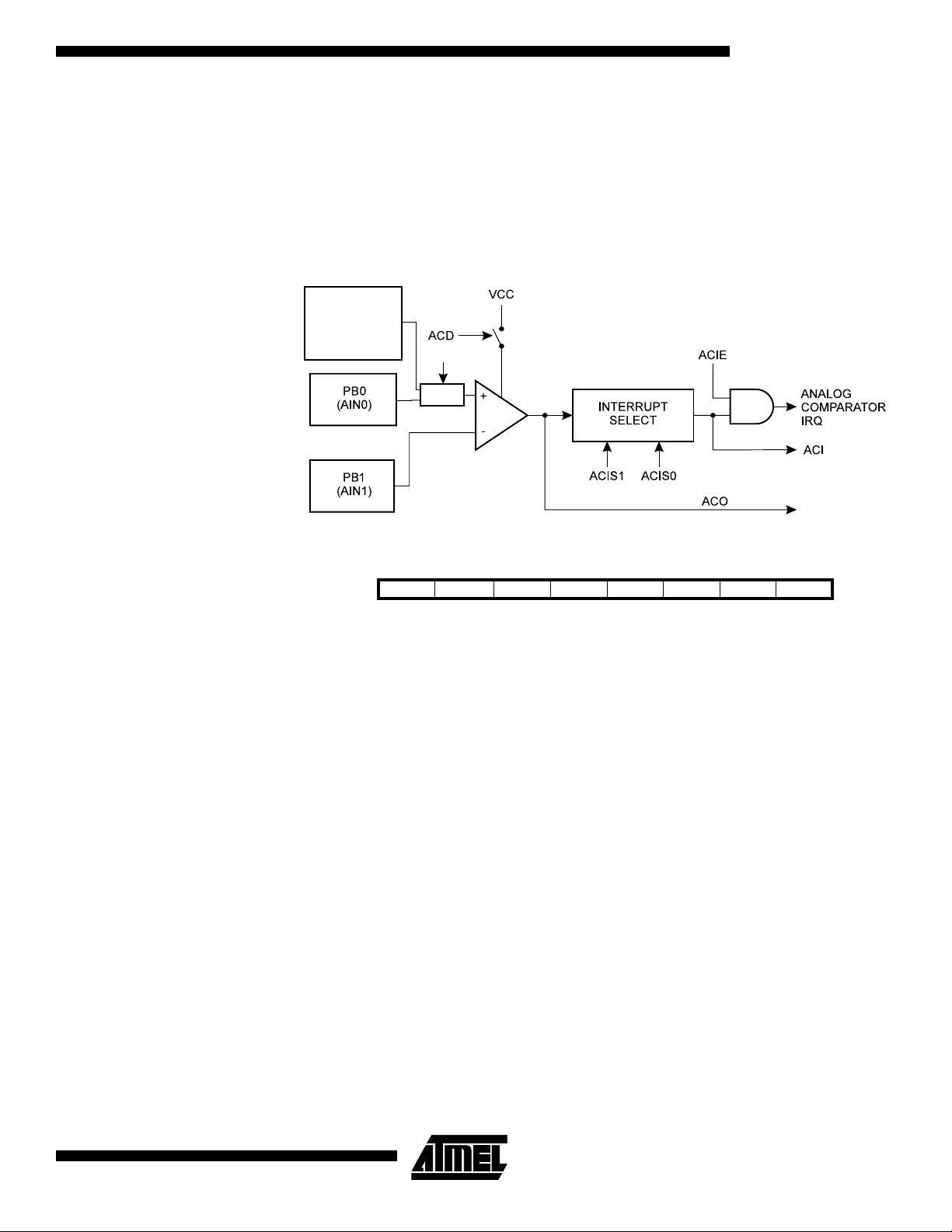
ATtiny11/12
Analog Comparator The Analog Comparator compares the input values on the positive input PB0 (AIN0) and
negative input PB1 (AIN1). When the voltage on the positive input PB0 (AIN0) is higher
than the voltage on the negative input PB1 (AIN1), the Analog Comparator Output
(ACO) is set (one). The comparator’s output can trigger a separate interrupt, exclusive
to the Analog Comparator. The user can select interrupt triggering on comparator output
rise, fall or toggle. A block diagram of the comparator and its surrounding logic is shown
in Figure 26.
Figure 26. Analog Comparator Block Diagram.
INTERNAL
VOLTAGE
REFERENCE
(ATtiny12 ONLY)
AINBG
MUX
Analog Comparator Control and Status Register – ACSR
Bit 76543210
$08 ACD (AINBG) ACO ACI ACIE - ACIS1 ACIS0 ACSR
Read/Write R/W R(/W) R R/W R/W R R/W R/W
Initial Value 0 0 X 0 0 0 0 0
Note: AINBG is only available in ATtiny12.
• Bit 7 - ACD: Analog Comparator Disable
When this bit is set (one), the power to the Analog Comparator is switched off. This bit
can be set at any time to turn off the Analog Comparator. When changing the ACD bit,
the Analog Comparator Interrupt must be disabled by clearing the ACIE bit in ACSR.
Otherwise an interrupt can occur when the bit is changed.
• Bit 6 - AINBG: Analog Comparator Bandgap Select in ATtiny12
In ATtiny12, when this bit is set, a fixed bandgap voltage of 1.22 ± 0.05V replaces the
normal input to the positive input (AIN0) of the comparator. When this bit is cleared, the
normal input pin PB0 is applied to the positive input of the comparator.
• Bit 6- Res: Reserved Bit in ATtiny11
This bit is a reserved bit in the ATtiny11 and will always read as zero.
• Bit 5 - ACO: Analog Comparator Output
ACO is directly connected to the comparator output.
• Bit 4 - ACI: Analog Comparator Interrupt Flag
1006C–09/01
This bit is set (one) when a comparator output event triggers the interrupt mode defined
by ACI1 and ACI0. The Analog Comparator Interrupt routine is executed if the ACIE bit
is set (one) and the I-bit in SREG is set (one). ACI is cleared by hardware when executing the corresponding interrupt handling vector. Alternatively, ACI is cleared by writing a
logic one to the flag.
39
Page 40

• Bit 3 - ACIE: Analog Comparator Interrupt Enable
When the ACIE bit is set (one) and the I-bit in the Status Register is set (one), the Analog Comparator Interrupt is activated. When cleared (zero), the interrupt is disabled.
• Bit 2 - Res: Reserved Bit
This bit is a reserved bit in the ATtiny11/12 and will always read as zero.
• Bits 1,0 - ACIS1, ACIS0: Analog Comparator Interrupt Mode Select
These bits determine which comparator events that trigger the Analog Comparator Interrupt. The different settings are shown in Table 18.
Table 18. ACIS1/ACIS0 Settings
ACIS1 ACIS0 Interrupt Mode
0 0 Comparator Interrupt on Output Toggle
01Reserved
1 0 Comparator Interrupt on Falling Output Edge
1 1 Comparator Interrupt on Rising Output Edge
Note: When changing the ACIS1/ACIS0 bits, the Analog Comparator Interrupt must be dis-
abled by clearing its interrupt enable bit in the ACSR register. Otherwise, an interrupt can
occur when the bits are changed.
Caution: Using the SBI or CBI instruction on bits other than ACI in this register will write
a one back into ACI if it is read as set, thus clearing the flag.
40
ATtiny11/12
1006C–09/01
Page 41

ATtiny11/12
I/O Port B All AVR ports have true read-modify-write functionality when used as general digital I/O
ports. This means that the direction of one port pin can be changed without unintentionally changing the direction of any other pin with the SBI and CBI instructions. The same
applies for changing drive value (if configured as output) or enabling/disabling of pull-up
resistors (if configured as input).
Port B is a 6-bit bi-directional I/O port.
Three I/O memory address locations are allocated for Port B, one each for the Data
Register – PORTB, $18, Data Direction Register – DDRB, $17, and the Port B Input
Pins – PINB, $16. The Port B Input Pins address is read only, while the Data Register
and the Data Direction Register are read/write.
Ports PB5..3 have special functions as described in the section “Pin Descriptions” on
page 5. If PB5 is not configured as external reset, it is input with no pull-up. On
ATtiny12, it can also output a logical zero, acting as an open-drain output. Note that,
since PB5 only has one possible output value, the output functionality of this pin is controlled by the DDRB register alone. If PB4 and/or PB3 are not used for clock function,
they are I/O pins. All I/O pins have individually selectable pull-ups.
The Port B output buffers on PB0 to PB4 can sink 20 mA and thus drive LED displays
directly. On ATtiny12, PB5 can sink 12 mA. When pins PB0 to PB4 are used as inputs
and are externally pulled low, they will source current (I
activated.
) if the internal pull-ups are
IL
The Port B pins with alternate functions are shown in Table 19:
Table 19. Port B Pins Alternate Functions
Port Pin Alternate Functions Device
PB0
PB1
PB2
PB3 XTAL1 (Oscillator Input) ATtiny11/12
PB4 XTAL2 (Oscillator Output) ATtiny11/12
PB5 RESET
AIN0 (Analog Comparator Positive Input) ATtiny11/12
MOSI (Data Input Line for Memory Downloading) ATtiny12
INT0 (External Interrupt0 Input) ATtiny11/12
AIN1 (Analog Comparator Negative Input) ATtiny11/12
MOSI (Data Output Line for Memory Downloading) ATtiny12
T0 (Timer/Counter0 External Counter Input) ATtiny11/12
SCK (Serial Clock Input for Serial Programming) ATtiny12
(External Reset Pin) ATtiny11/12
When the pins PB2..0 are used for the alternate function, the DDRB and PORTB register has to be set according to the alternate function description. When PB5..3 are used
for alternate functions, the values in the corresponding DDRB and PORTB bits are
ignored.
1006C–09/01
41
Page 42

Port B Data Register – PORTB
Bit 76543210
$18
Read/Write R R R R/W R/W R/W R/W R/W
Initial Value 0 0 0 0 0 0 0 0
- - - PORTB4 PORTB3 PORTB2 PORTB1 PORTB0 PORTB
Port B Data Direction Register – DDRB
Bit 76543210
$17 - - (DDB5) DDB4 DDB3 DDB2 DDB1 DDB0 DDRB
Read/Write R R R(/W) R/W R/W R/W R/W R/W
Initial Value 0 0 0 0 0 0 0 0
Note: DDB5 is only available in ATtiny12.
Port B Input Pins Address – PINB
Bit 76543210
$16 - - PINB5 PINB4 PINB3 PINB2 PINB1 PINB0 PINB
Read/WriteRRRRRRRR
Initial Value 0 0 N/A N/A N/A N/A N/A N/A
The Port B Input Pins address – PINB – is not a register, and this address enables
access to the physical value on each Port B pin. When reading PORTB, the Port B Data
Latch is read, and when reading PINB, the logical values present on the pins are read.
Port B as General Digital I/O The lowermost five pins in port B have equal functionality when used as digital I/O pins.
PBn, General I/O pin: The DDBn bit in the DDRB register selects the direction of this
pin, if DDBn is set (one), PBn is configured as an output pin. If DDBn is cleared (zero),
PBn is configured as an input pin. If PORTBn is set (one) when the pin is configured as
an input pin, the MOS pull-up resistor is activated. On ATtiny12 this feature can be disabled by setting the Pull-up Disable (PUD) bit in the MCUCR register. To switch the pullup resistor off, the PORTBn can be cleared (zero), the pin can be configured as an output pin, or in ATtiny12, the PUD bit can be set. The port pins are tri-stated when a reset
condition becomes active, even if the clock is not running.
Table 20. DDBn Effects on Port B Pins
DDBn PORTBn I/O Pull-up Comment
0 0 Input No Tri-state (Hi-Z)
0 1 Input Yes
1 0 Output No Push-pull Zero Output
1 1 Output No Push-pull One Output
PBn will source current if ext. pulled low. In ATtiny12
pull-ups can be disabled by setting the PUD bit.
n: 4,3…0, pin number.
Note that in ATtiny11, PB5 is input only. On ATtiny12, PB5 is input or open-drain output.
Because this pin is used for 12V programming, there is no ESD protection diode limiting
the voltage on the pin to V
the voltage on this pin does not rise above V
+ 0.5V. Thus, special care should be taken to ensure that
CC
+ 1V during normal operation. This may
CC
cause the MCU to reset or enter programming mode unintentionally.
42
ATtiny11/12
1006C–09/01
Page 43

ATtiny11/12
Alternate Functions of Port B All port B pins are connected to a pin change detector that can trigger the pin change
interrupt. See “Pin Change Interrupt” on page 27 for details. In addition, Port B has the
following alternate functions:
• RESET
When the RSTDISBL fuse is unprogrammed, this pin serves as external reset. When
the RSTDISBL fuse is programmed, this pin is a general input pin. In ATtiny12, it is also
an open-drain output pin.
• XTAL2 - Port B, Bit 4
XTAL2, oscillator output. When this pin is not used for clock purposes, it is a general I/O
pin. Refer to section “Pin Descriptions” on page 5 for details.
• XTAL1 - Port B, Bit 3
XTAL1, oscillator or clock input. When this pin is not used for clock purposes, it is a general I/O pin. Refer to section “Pin Descriptions” on page 5 for details.
• T0/SCK - Port B, Bit 2
This pin can serve as the external counter clock input. See the timer/counter description
for further details. If external timer/counter clocking is selected, activity on this pin will
clock the counter even if it is configured as an output. In ATtiny12 and serial programming mode, this pin serves as the serial clock input, SCK.
• INT0/AIN1/MISO - Port B, Bit 1
- Port B, Bit 5
This pin can serve as the external interrupt0 input. See the interrupt description for
details on how to enable this interrupt. Note that activity on this pin will trigger the interrupt even if the pin is configured as an output. This pin also serves as the negative input
of the on-chip Analog Comparator. In ATtiny12 and serial programming mode, this pin
serves as the serial data input, MISO.
• AIN0/MOSI - Port B, Bit 0
This pin also serves as the positive input of the on-chip Analog Comparator. In ATtiny12
and serial programming mode, this pin serves as the serial data output, MOSI.
During Power-down Mode, the schmitt triggers of the digital inputs are disconnected on
the Analog Comparator input pins. This allows an analog voltage close to V
present during power-down without causing excessive power consumption.
/2 to be
CC
1006C–09/01
43
Page 44

Memory Programming
Program (and Data) Memory Lock Bits
The ATtiny11/12 MCU provides two lock bits which can be left unprogrammed (“1”) or
can be programmed (“0”) to obtain the additional features listed in Table 21
bits can only be erased with the Chip Erase command
.
Table 21. Lock Bit Protection Modes
Memory Lock Bits
Protection TypeMode LB1 LB2
1 1 1 No memory lock features enabled.
201
3 0 0 Same as mode 2, and verify is also disabled.
Note: 1. In the High-voltage Serial Programming mode, further programming of the fuse bits
are also disabled. Program the fuse bits before programming the lock bits.
Further programming of the Flash (and EEPROM for ATtiny12) is
disabled.
(1)
Fuse Bits in ATtiny11 The ATtiny11 has five fuse bits, FSTRT, RSTDISBL and CKSEL2..0.
• FSTRT: See Table 7, “Start-up Times for the ATtiny11 (V
which value to use. Default value is unprogrammed (“1”).
• When RSTDISBL is programmed (“0”), the external reset function of pin PB5 is
disabled.
(1)
Default value is unprogrammed (“1”).
• CKSEL2..0: See Table 3, “Device Clocking Options Select,” on page 5, for which
combination of CKSEL2..0 to use. Default value is “100”, internal RC oscillator.
= 2.7V),” on page 18 for
CC
. The lock
The status of the fuse bits is not affected by Chip Erase.
Note: 1. If the RSTDISBL Fuse is programmed, then the programming hardware should apply
+12V to PB5 while the ATtiny11 is in Power-on Reset. If not, the part can fail to enter
programming mode caused by drive contention on PB0.
Fuse Bits in ATtiny12 The ATtiny12 has eight fuse bits, BODLEVEL, BODEN, SPIEN, RSTDISBL and
CKSEL3..0. All the fuse bits are programmable in both High-voltage and Low-voltage
Serial programming modes. Changing the fuses does not have any effect while in programming mode.
• The BODLEVEL Fuse selects the Brown-out Detection level and changes the start-
up times. See “Brown-out Detection (ATtiny12)” on page 22. See Table 9, “AT ti ny 1 2
Clock Options and Start-up Times,” on page 20. Default value is programmed (“0”).
• When the BODEN Fuse is programmed (“0”), the Brown-out Detector is enabled.
See “Brown-out Detection (ATtiny12)” on page 22. Default value is unprogrammed
(“1”).
• When the SPIEN Fuse bit is programmed (“0”), Low-Voltage Serial Program and
Data Downloading is enabled. Default value is programmed (“0”). Unprogramming
this fuse while in the Low-Voltage Serial Programming mode will disable future insystem downloading attempts.
• When the RSTDISBL Fuse is programmed (“0”), the external reset function of pin
PB5 is disabled.
while in the Low-Voltage Serial Programming mode will disable future in-system
downloading attempts.
(1)
Default value is unprogrammed (“1”). Programming this fuse
44
ATtiny11/12
1006C–09/01
Page 45

ATtiny11/12
• CKSEL3..0 fuses: See Table 3, “Device Clocking Options Select,” on page 5 and
Ta bl e 9 , “ATtiny12 Clock Options and Start-up Times,” on page 20, for which
combination of CKSEL3..0 to use. Default value is “0010”, internal RC oscillator with
long start-up time.
The status of the fuse bits is not affected by Chip Erase.
Note: 1. If the RSTDISBL Fuse is programmed, then the programming hardware should apply
+12V to PB5 while the ATtiny12 is in Power-on Reset. If not, the part can fail to enter
programming mode caused by drive contention on PB0 and/or PB5.
Signature Bytes All Atmel microcontrollers have a three-byte signature code which identifies the device.
The three bytes reside in a separate address space.
For the ATtiny11 they are:
1. $000: $1E (indicates manufactured by Atmel)
2. $001: $90 (indicates 1 Kb Flash memory)
3. $002: $04 (indicates ATtiny11 device when signature byte $001 is $90)
For the ATtiny12
1. $000: $1E (indicates manufactured by Atmel)
2. $001: $90 (indicates 1 Kb Flash memory)
3. $002: $05 (indicates ATtiny12 device when signature byte $001 is $90)
Note: 1. When both lock bits are programmed (Lock mode 3), the Signature Bytes can not be
(1)
they are:
read in the Low-voltage Serial mode. Reading the Signature Bytes will return: $00,
$01 and $02.
Calibration Byte in ATtiny 12
The ATtiny12 has a one-byte calibration value for the internal RC oscillator. This byte
resides in the high byte of address $000 in the signature address space. During memory
programming, the external programmer must read this location and program its value
into a selected location in the normal Flash Program memory. At start-up, the user software must read this Flash location and write the value to the OSCCAL register.
Programming the Flash and EEPROM
ATt iny 11 Atmel’s ATtiny11 offers 1K bytes of Flash Program memory.
The ATtiny11 is shipped with the on-chip Flash Program memory array in the erased
state (i.e., contents = $FF) and ready to be programmed.
This device supports a High-voltage (12V) Serial programming mode. Only minor currents (<1 mA) are drawn from the +12V pin during programming.
The program memory array in the ATtiny11 is programmed byte-by-byte.
ATt iny 12 Atmel’s ATtiny12 offers 1K bytes of in-system reprogrammable Flash Program memory
and 64 bytes of in-system reprogrammable EEPROM Data memory.
The ATtiny12 is shipped with the on-chip Flash Program and EEPROM Data memory
arrays in the erased state (i.e., contents = $FF) and ready to be programmed.
This device supports a high-voltage (12V) serial programming mode and a low-voltage
serial programming mode. The +12V is used for programming enable only, and no current of significance is drawn by this pin. The Low-voltage Serial Programming mode
1006C–09/01
45
Page 46
provides a convenient way to download program and data into the ATtiny12 inside the
user’s system.
The program and data memory arrays in the ATtiny12 are programmed byte-by-byte in
either programming mode. For the EEPROM, an auto-erase cycle is provided within the
self-timed write instruction in the Low-voltage Serial Programming mode.
ATtiny11/12 During programming, the supply voltage must be in accordance with Table 22.
Table 22. Supply Voltage during Programming
Part Low-voltage Serial Programming High-voltage Serial Programming
ATtiny11L Not applicable 4.5 - 5.5V
ATtiny11 Not applicable 4.5 - 5.5V
ATtiny12V 2.2 - 5.5V 4.5 - 5.5V
ATtiny12L 2.7 - 5.5V 4.5 - 5.5V
ATtiny12 4.0 - 5.5V 4.5 - 5.5V
High-voltage Serial Programming
This section describes how to program and verify Flash Program memory, EEPROM
Data memory (ATtiny12), lock bits and fuse bits in the ATtiny11/12.
Figure 27. High-voltage Serial Programming
11.5 - 12.5V 4.5 - 5.5V
ATtiny
SERIAL CLOCK INPUT
PB5 (RESET)
PB3 (XTAL1)
GND
VCC
PB2
PB1
PB0
SERIAL DATA OUTPUT
SERIAL INSTR. INPUT
SERIAL DATA INPUT
46
ATtiny11/12
1006C–09/01
Page 47

ATtiny11/12
High-voltage Serial Programming Algorithm
To program and verify the ATtiny11/12 in the High-voltage Serial Programming mode,
the following sequence is recommended (See instruction formats in Table 23):
1. Power-up sequence: Apply 4.5 - 5.5V between V
to “0” and wait at least 100 ns. Toggle PB3 at least four times with minimum 100
ns pulse-width. Set PB3 to “0”. Wait at least 100 ns. Apply 12V to PB5 and wait
at least 100 ns before changing PB0. Wait 8 µs before giving any instructions.
2. The Flash array is programmed one byte at a time by supplying first the address,
then the low and high data byte. The write instruction is self-timed, wait until the
PB2 (RDY/BSY
3. The EEPROM array (ATtiny12 only) is programmed one byte at a time by supply-
ing first the address, then the data byte. The write instruction is self-timed, wait
until the PB2 (RDY/BSY
4. Any memory location can be verified by using the Read instruction which returns
the contents at the selected address at serial output PB2.
5. Power-off sequence:Set PB3 to “0”.
Set PB5 to “1”.
Tu r n V
CC
When writing or reading serial data to the ATtiny11/12, data is clocked on the rising
edge of the serial clock, see Figure 28, Figure 29 and Table 24 for details.
) pin goes high.
) pin goes high.
power off.
and GND. Set PB5 and PB0
CC
1006C–09/01
47
Page 48

Figure 28. High-voltage Serial Programming Waveforms
SERIAL DATA INPUT
PB0
MSB
LSB
SERIAL INSTR. INPUT
PB1
SERIAL DATA OUTPUT
PB2
SERIAL CLOCK INPUT
XTAL1/PB3
MSB
MSB LSB
012345678910
Table 23. High-voltage Serial Programming Instruction Set for ATtiny11/12
Instruction Format
Instruction
0_0000_0000_00
0_0110_1100_00
x_xxxx_xxxx_xx
0_bbbb_bbbb_00
0_0000_1100_00
x_xxxx_xxxx_xx
0_0000_0000_00
0_0110_1100_00
0_0000_0000_00
0_0000_0000_00
0_0111_1100_00
0_0000_0000_00
0_bbbb_bbbb_00
0_0000_1100_00
x_xxxx_xxxx_xx
0_0000_0000_00
0_0110_1100_00
0_0000_0000_00
Chip Erase
Write Flash
High and Low
Address
Write Flash Low
byte
Write Flash
High byte
Read Flash
High and Low
Address
Read Flash
Low byte
Read Flash
High byte
Write EEPROM
Low Address
(ATtiny12)
Write EEPROM
byte (ATtiny12)
Read EEPROM
Low Address
(ATtiny12)
PB0
PB1
PB2
PB0
PB1
PB2
PB0
PB1
PB2
PB0
PB1
PB2
PB0
PB1
PB2
PB0
PB1
PB2
PB0
PB1
PB2
PB0
PB1
PB2
PB0
PB1
PB2
PB0
PB1
PB2
0_1000_0000_00
0_0100_1100_00
x_xxxx_xxxx_xx
0_0001_0000_00
0_0100_1100_00
x_xxxx_xxxx_xx
0_ i i i i_i i i i _00
0_0010_1100_00
x_xxxx_xxxx_xx
0_ i i i i_i i i i _00
0_0011_1100_00
x_xxxx_xxxx_xx
0_0000_0010_00
0_0100_1100_00
x_xxxx_xxxx_xx
0_0000_0000_00
0_0110_1000_00
x_xxxx_xxxx_xx
0_0000_0000_00
0_0111_1000_00
x_xxxx_xxxx_xx
0_0001_0001_00
0_0100_1100_00
x_xxxx_xxxx_xx
0_ i i i i_i i i i _00
0_0010_1100_00
x_xxxx_xxxx_xx
0_0000_0011_00
0_0100_1100_00
x_xxxx_xxxx_xx
0_0000_0000_00
0_0110_0100_00
x_xxxx_xxxx_xx
0_0000_000a_00
0_0001_1100_00
x_xxxx_xxxx_xx
0_0000_0000_00
0_0110_0100_00
x_xxxx_xxxx_xx
0_0000_0000_00
0_0111_0100_00
x_xxxx_xxxx_xx
0_0000_000a_00
0_0001_1100_00
x_xxxx_xxxx_xx
0_0000_0000_00
0_0110_1100_00
o_oooo_ooox_xx
0_0000_0000_00
0_0111_1100_00
o_oooo_ooox_xx
0_00bb_bbbb_00
0_0000_1100_00
x_xxxx_xxxx_xx
0_0000_0000_00
0_0110_0100_00
x_xxxx_xxxx_xx
0_00bb_bbbb_00
0_0000_1100_00
x_xxxx_xxxx_xx
LSB
0_0000_0000_00
0_0100_1100_00
x_xxxx_xxxx_xx
Operation RemarksInstr.1 Instr.2 Instr.3 Instr.4
Wait after Instr.4 until PB2 goes
high for the Chip Erase cycle to
finish.
Repeat Instr.2 for a new 256 byte
page. Repeat Instr.3 for each new
address.
Wait after Instr.3 until PB2 goes
high. Repeat Instr.1, Instr. 2 and
Instr.3 for each new address.
Wait after Instr.3 until PB2 goes
high. Repeat Instr.1, Instr. 2 and
Instr.3 for each new address.
Repeat Instr.2 and Instr.3 for each
new address.
Repeat Instr.1 and Instr.2 for each
new address.
Repeat Instr.1 and Instr.2 for each
new address.
Repeat Instr.2 for each new
address.
Wait after Instr.3 until PB2 goes
high
Repeat Instr.2 for each new
address.
48
ATtiny11/12
1006C–09/01
Page 49

Table 23. High-voltage Serial Programming Instruction Set for ATtiny11/12 (Continued)
Instruction Format
ATtiny11/12
Instruction
0_0000_0000_00
Read EEPROM
byte (ATtiny12)
Write Fuse bits
(ATtiny11)
Write Fuse bits
(ATtiny12)
Write Lock bits
Read Fuse bits
(ATtiny11)
Read Fuse bits
(ATtiny12)
Read Lock bits
Read Signature
Bytes
Read
Calibration Byte
(ATtiny12)
PB0
PB1
PB2
PB0
PB1
PB2
PB0
PB1
PB2
PB0
PB1
PB2
PB0
PB1
PB2
PB0
PB1
PB2
PB0
PB1
PB2
PB0
PB1
PB2
PB0
PB1
PB2
0_0110_1000_00
x_xxxx_xxxx_xx
0_0100_0000_00
0_0100_1100_00
x_xxxx_xxxx_xx
0_0100_0000_00
0_0100_1100_00
x_xxxx_xxxx_xx
0_0010_0000_00
0_0100_1100_00
x_xxxx_xxxx_xx
0_0000_0100_00
0_0100_1100_00
x_xxxx_xxxx_xx
0_0000_0100_00
0_0100_1100_00
x_xxxx_xxxx_xx
0_0000_0100_00
0_0100_1100_00
x_xxxx_xxxx_xx
0_0000_1000_00
0_0100_1100_00
x_xxxx_xxxx_xx
0_0000_1000_00
0_0100_1100_00
x_xxxx_xxxx_xx
Note: a = address high bits
b = address low bits
i = data in
o = data out
x = don’t care
1 = Lock Bit1
2 = Lock Bit2
3 = CKSEL0 Fuse
4 = CKSEL1 Fuse
5 = CKSEL2 Fuse
9, 6 = RSTDISBL Fuse
7 = FSTRT Fuse
8 = CKSEL3 Fuse
A = SPIEN Fuse
B = BODEN Fuse
C = BODLEVEL Fuse
0_0000_0000_00
0_0110_1100_00
o_oooo_ooox_xx
0_0007_6543_00
0_0010_1100_00
x_xxxx_xxxx_xx
0_CBA9_8543_00
0_0010_1100_00
x_xxxx_xxxx_xx
0_0000_0210_00
0_0010_1100_00
x_xxxx_xxxx_xx
0_0000_0000_00
0_0110_1000_00
x_xxxx_xxxx_xx
0_0000_0000_00
0_0110_1000_00
x_xxxx_xxxx_xx
0_0000_0000_00
0_0111_1000_00
x_xxxx_xxxx_xx
0_0000_00bb_00
0_0000_1100_00
x_xxxx_xxxx_xx
0_0000_0000_00
0_0000_1100_00
x_xxxx_xxxx_xx
0_0000_0000_00
0_0110_0100_00
x_xxxx_xxxx_xx
0_0000_0000_00
0_0110_0100_00
x_xxxx_xxxx_xx
0_0000_0000_00
0_0110_0100_00
x_xxxx_xxxx_xx
0_0000_0000_00
0_0110_1100_00
x_xx76_543x_xx
0_0000_0000_00
0_0110_1100_00
C_BA98_543x_xx
0_0000_0000_00
0_0111_1100_00
x_xxxx_21xx_xx
0_0000_0000_00
0_0110_1000_00
x_xxxx_xxxx_xx
0_0000_0000_00
0_0111_1000_00
x_xxxx_xxxx_xx
0_0000_0000_00
0_0110_1100_00
x_xxxx_xxxx_xx
0_0000_0000_00
0_0110_1100_00
x_xxxx_xxxx_xx
0_0000_0000_00
0_0110_1100_00
0_0000_0000_00
0_0000_0000_00
0_0110_1100_00
o_oooo_ooox_xx
0_0000_0000_00
0_0111_1100_00
o_oooo_ooox_xx
Operation RemarksInstr.1 Instr.2 Instr.3 Instr.4
Repeat Instr.2 for each new
address
Wait
t
WLWH_PFB
Write fuse bits cycle to finish. Write
7 - 3 = “0” to program the fuse bit.
Wait after Instr.4 until PB2 goes
high. Write C - A, 9, 8, 5 - 3 = “0” to
program the fuse bit.
Wait after Instr.4 until PB2 goes
high. Write 2, 1 = “0” to program the
lock bit.
Reading 7 - 3 = “0” means the fuse
bit is programmed.
Reading C - A, 9, 8, 5 - 3 = “0”
means the fuse bit is programmed.
Reading 2, 1 = “0” means the lock
bit is programmed.
Repeat Instr.2 - Instr.4 for each
signature byte address
after Instr.3 for the
1006C–09/01
49
Page 50

High-voltage Serial Programming Characteristics
Figure 29. High-voltage Serial Programming Timing
SDI (PB0), SII (PB1)
t
IVSH
SCI (PB3)
SDO (PB2)
t
SHSL
t
SHOV
t
SHIX
t
SLSH
Low-voltage Serial Downloading (ATtiny12 only)
Table 24. High-voltage Serial Programming Characteristics T
= 25°C ± 10%, VCC =
A
5.0V ± 10% (Unless otherwise noted)
Symbol Parameter Min Typ Max Units
t
SHSL
t
SLSH
t
IVSH
t
SHIX
t
SHOV
t
WLWH_PFB
SCI (PB3) Pulse Width High 100 ns
SCI (PB3) Pulse Width Low 100 ns
SDI (PB0), SII (PB1) Valid to SCI (PB3) High 50 ns
SDI (PB0), SII (PB1) Hold after SCI (PB3) High 50 ns
SCI (PB3) High to SDO (PB2) Valid 10 16 32 ns
Wait after Instr. 3 for Write Fuse Bits 1.7 2.5 3.4 ms
Both the program and data memory arrays can be programmed using the SPI bus while
RESET
MISO (output), see Figure 30. After RESET
is pulled to GND. The serial interface consists of pins SCK, MOSI (input) and
is set low, the Programming Enable instruc-
tion needs to be executed first before program/erase instructions can be executed.
Figure 30. Serial Programming and Verify
2.2 - 5.5V
ATtiny12
GND
PB5 (RESET) VCC
50
ATtiny11/12
GND
PB2
PB1
PB0
SCK
MISO
MOSI
1006C–09/01
Page 51

ATtiny11/12
If the chip Erase command in Low-voltage Serial Programming is executed only once,
one data byte may be written to the flash after erase. Using the following algorithm guarantees that the flash will be erased:
• Execute a chip erase command
• Write $FF to address $00 in the flash
• Execute a second chip erase command
For the EEPROM, an auto-erase cycle is provided within the self-timed write instruction
and there is no need to first execute the Chip Erase instruction. The Chip Erase instruction turns the content of every memory location in both the program and EEPROM
arrays into $FF.
The program and EEPROM memory arrays have separate address spaces:
$0000 to $01FF for program memory and $000 to $03F for EEPROM memory.
The device can be clocked by any clock option during Low-voltage Serial Programming.
The minimum low and high periods for the serial clock (SCK) input are defined as
follows:
Low: > 2 MCU clock cycles
High: > 2 MCU clock cycles
Low-voltage Serial Programming Algorithm
When writing serial data to the ATtiny12, data is clocked on the rising edge of SCK.
When reading data from the ATtiny12, data is clocked on the falling edge of SCK. See
Figure 31, Figure 32 and Table 26 for timing details. To program and verify the ATtiny12
in the serial programming mode, the following sequence is recommended (See 4 byte
instruction formats in Table 25
):
1. Power-up sequence:
Apply power between VCC and GND while RESET and SCK are set to “0”. In accordance with the setting of CKSEL fuses, apply a crystal/resonator, external clock or
RC network, or let the device run on the internal RC oscillator. In some systems, the
programmer can not guarantee that SCK is held low during power-up. In this case,
RESET
must be given a positive pulse of at least two MCU cycles duration after
SCK has been set to “0”.
2. Wait for at least 20 ms and enable serial programming by sending the Program-
ming Enable Serial instruction to the MOSI (PB0) pin.
3. The serial programming instructions will not work if the communication is out of
synchronization. When in sync, the second byte ($53) will echo back when issuing the third byte of the Programming Enable instruction. Whether the echo is
correct or not, all 4 bytes of the instruction must be transmitted. If the $53 did not
echo back, give SCK a positive pulse and issue a new Programming Enable
instruction. If the $53 is not seen within 32 attempts, there is no functional device
connected.
4. If a Chip Erase is performed (must be done to erase the Flash), wait t
after the instruction, give RESET
See Table 27 on page 54 for t
a positive pulse, and start over from Step 2.
WD_ERASE
value.
WD_ERASE
5. The Flash or EEPROM array is programmed one byte at a time by supplying the
address and data together with the appropriate Write instruction. An EEPROM
memory location is first automatically erased before new data is written. Use
Data Polling to detect when the next byte in the Flash or EEPROM can be written. If polling is not used, wait t
WD_FLASH
or t
WD_EEPROM
before transmitting the
1006C–09/01
51
Page 52

next instruction. See Table 28 on page 54 for t
WD_FLASH
and t
WD_EEPROM
values. In
an erased device, no $FFs in the data file(s) needs to be programmed.
6. Any memory location can be verified by using the Read instruction which returns
the content at the selected address at the serial output MISO (PB1) pin.
7. At the end of the programming session, RESET
can be set high to commence
normal operation.
8. Power-off sequence (if needed):
Set XTAL1 to “0” (if external clocking is used).
Set RESET
Turn V
to “1”.
power off.
CC
Data Polling When a byte is being programmed into the Flash or EEPROM, reading the address
location being programmed will give the value $FF. At the time the device is ready for a
new byte, the programmed value will read correctly. This is used to determine when the
next byte can be written. This will not work for the value $FF, so when programming this
value, the user will have to wait for at least t
WD_FLASH
or t
WD_EEPROM
before programming
the next byte. As a chip-erased device contains $FF in all locations, programming of
addresses that are meant to contain $FF can be skipped. This does not apply if the
EEPROM is reprogrammed without chip-erasing the device. In that case, data polling
cannot be used for the value $FF, and the user will have to wait at least t
before programming the next byte. See Table 28 for t
WD_FLASH
and t
WD_EEPROM
WD_EEPROM
values.
Figure 31. Low-voltage Serial Programming Waveforms
SERIAL DATA INPUT
PB0(MOSI)
SERIAL DATA OUTPUT
PB1(MISO)
SERIAL CLOCK INPUT
PB2(SCK)
MSB
MSB
LSB
LSB
52
ATtiny11/12
1006C–09/01
Page 53

Table 25. Low-voltage Serial Programming Instruction Set
Instruction Format
Instruction
ATtiny11/12
OperationByte 1 Byte 2 Byte 3 Byte4
Programming Enable
Chip Erase
Read Program Memory
Write Program Memory
Read EEPROM
Memory
Write EEPROM
Memory
Write Lock Bits
Read Lock Bits
Read Signature Bytes 0011 0000 xxxx xxxx 0000 00bb oooo oooo Read signature byte o at address b.
Read Calibration Byte 0011 1000 xxxx xxxx 0000 0000 oooo oooo
Write Fuse Bits
1010 1100 0101 0011 xxxx xxxx xxxx xxxx Enable serial programming while
is low.
RESET
1010 1100 100x xxxx xxxx xxxx xxxx xxxx Chip erase Flash and EEPROM
memory arrays.
0010 H000 xxxx xxxa bbbb bbbb oooo oooo Read H (high or low) data o from
program memory at word address
a:b.
0100 H000 xxxx xxxa bbbb bbbb iiii iiii Write H (high or low) data i to
program memory at word address
a:b.
1010 0000 xxxx xxxx xxbb bbbb oooo oooo Read data o from EEPROM memory
at address b.
1100 0000 xxxx xxxx xxbb bbbb iiii iiii Write data i to EEPROM memory at
address b.
1010 1100 1111 1211 xxxx xxxx xxxx xxxx Write lock bits. Set bits 1,2 = “0” to
program lock bits.
0101 1000 xxxx xxxx xxxx xxxx xxxx x21x Read lock bits. “0” = programmed, “1”
= unprogrammed.
1010 1100 101x xxxx xxxx xxxx A987 6543 Set bits A, 9 - 3 = “0” to program, “1”
to unprogram.
(1)
Read Fuse Bits
Note: a = address high bits
b = address low bits
H = 0 - Low byte, 1 - High byte
o = data out
i = data in
x = don’t care
1 = Lock bit 1
2 = Lock bit 2
3 = CKSEL0 Fuse
4 = CKSEL1 Fuse
5 = CKSEL2 Fuse
6 = CKSEL3 Fuse
7 = RSTDISBL Fuse
8 = SPIEN Fuse
9 = BODEN Fuse
A = BODLEVEL Fuse
Note: 1. The signature bytes are not readable in Lock mode 3, i.e. both lock bits programmed.
0101 0000 xxxx xxxx xxxx xxxx A987 6543 Read fuse bits. “0” = programmed, “1”
= unprogrammed.
1006C–09/01
53
Page 54

Low-voltage Serial Programming Characteristics
Figure 32. Low-voltage Serial Programming Timing
MOSI
t
OVSH
t
SHOX
t
SLSH
SCK
t
SHSL
MISO
t
SLIV
Table 26. Low-voltage Serial Programming Characteristics T
= 2.2 - 5.5V (Unless otherwise noted)
V
CC
= -40°C to 85°C,
A
Symbol Parameter Min Typ Max Units
1/t
t
CLCL
1/t
t
CLCL
1/t
t
CLCL
t
SHSL
t
SLSH
t
OVSH
t
SHOX
t
SLIV
CLCL
CLCL
CLCL
Oscillator Frequency (VCC = 2.2 - 2.7V) 0 1 MHz
Oscillator Period (VCC = 2.2 - 2.7V) 1000 ns
Oscillator Frequency (VCC = 2.7 - 4.0V) 0 4 MHz
Oscillator Period (VCC = 2.7 - 4.0V) 250 ns
Oscillator Frequency (VCC = 4.0 - 5.5V) 0 8 MHz
Oscillator Period (VCC = 4.0 - 5.5V) 125 ns
SCK Pulse Width High 2 t
SCK Pulse Width Low 2 t
MOSI Setup to SCK High t
MOSI Hold after SCK High 2 t
CLCL
CLCL
CLCL
CLCL
SCK Low to MISO Valid 10 16 32 ns
ns
ns
ns
ns
54
ATtiny11/12
Table 27. Minimum Wait Delay after the Chip Erase Instruction
Symbol Minimum Wait Delay
t
WD_ERASE
6.8 ms
Table 28. Minimum Wait Delay after Writing a Flash or EEPROM Location
Symbol Minimum Wait Delay
t
WD_FLASH
t
WD_EEPROM
3.4 ms
6.8 ms
1006C–09/01
Page 55

Electrical Characteristics
Absolute Maximum Ratings
Operating Temperature.................................. -55°C to +125°C
Storage Temperature..................................... -65°C to +150°C
Voltage on any Pin except RESET
with respect to Ground ................................-1.0V to VCC+0.5V
Voltage on RESET
Maximum Operating Voltage ............................................ 6.0V
DC Current per I/O Pin ............................................... 40.0 mA
with respect to Ground......-1.0V to +13.0V
ATtiny11/12
*NOTICE: Stresses beyond those ratings listed under
“Absolute Maximum Ratings” may cause permanent damage to the device. This is a stress rating
only and functional operation of the device at
these or other conditions beyond those indicated
in the operational sections of this specification is
not implied. Exposure to absolute maximum rating conditions for extended periods may affect
device reliability.
DC Current
V
and GND Pins................................ 100.0 mA
CC
DC Characteristics – Preliminary Data
TA = -40°C to 85°C, VCC = 2.7V to 5.5V for ATtiny11, VCC = 1.8V to 5.5V for ATtiny12 (Unless otherwise noted)
Symbol Parameter Condition Min Typ Max Units
V
IL
V
IL1
V
IH
V
IH1
V
IH2
V
OL
V
OL
V
OH
I
IL
I
IH
R
I/O
Input Low Voltage Except (XTAL) -0.5 0.3 V
Input Low Voltage XTAL -0.5 0.1 V
4.3
2.3
CC
CC
CC
(2)
(2)
(2)
VCC + 0.5 V
VCC + 0.5 V
VCC + 0.5 V
Input High Voltage Except (XTAL, RESET) 0.6 V
Input High Voltage XTAL 0.7 V
Input High Voltage RESET 0.85 V
Output Low Voltage
(3)
Por t B
Output Low Voltage
PB5 (ATtiny12)
Output High Voltage
(4)
Por t B
Input Leakage Current
I/O Pin
Input Leakage Current
I/O Pin
= 20 mA, VCC = 5V
I
OL
IOL = 10 mA, VCC = 3V
IOL = 12 mA, VCC = 5V
= 6 mA, VCC = 3V
I
OL
I
= -3 mA, VCC = 5V
OH
= -1.5 mA, VCC = 3V
I
OH
VCC = 5.5V, Pin Low
(Absolute value)
VCC = 5.5V, Pin High
(Absolute value)
I/O Pin Pull-Up 35 122 kΩ
(1)
CC
(1)
CC
0.6
0.5
0.6
0.5
8.0 µA
8.0 µA
V
V
V
V
V
V
V
V
1006C–09/01
55
Page 56

DC Characteristics – Preliminary Data (Continued)
TA = -40°C to 85°C, VCC = 2.7V to 5.5V for ATtiny11, VCC = 1.8V to 5.5V for ATtiny12 (Unless otherwise noted)
Symbol Parameter Condition Min Typ Max Units
Active 1 MHz, V
(ATtiny12V)
CC
= 3V
1.0 mA
Active 2 MHz, V
(ATtiny11L)
Active 4 MHz, V
(ATtiny12L)
Active 6 MHz, V
(ATtiny11)
Active 8 MHz, V
(ATtiny12)
Idle 1 MHz, V
(ATtiny12V)
I
CC
Power Supply Current
Idle 2 MHz, V
(ATtiny11L)
Idle 4 MHz, V
(ATtiny12L)
Idle 6 MHz, V
(ATtiny11)
Idle 8 MHz, V
(ATtiny12)
Power Down
WDT enabled
Power Down
WDT disabled (ATtiny12)
Power Down
WDT disabled (ATtiny11)
= 3V
CC
= 3V
CC
= 5V
CC
= 5V
CC
= 3V
CC
= 3V
CC
= 3V
CC
= 5V
CC
= 5V
CC
(5)
, V
= 3V,
CC
(5)
, V
= 3V.
CC
(5)
, V
= 3V.
CC
9.0 15 µA
<1 2 µA
<1 5 µA
2.0 mA
2.5 mA
10 mA
10 mA
0.4 mA
0.5 mA
1.0 mA
2.0 mA
3.5 mA
V
ACIO
I
ACLK
T
ACPD
Analog Comparator
Input Offset Voltage
Analog Comparator
Input Leakage Current
Analog Comparator
Propagation Delay
VCC = 5V
V
= VCC/2
IN
VCC = 5V
= VCC/2
V
IN
VCC = 2.7V
V
= 4.0V
CC
-50 50 nA
Notes: 1. “Max” means the highest value where the pin is guaranteed to be read as low.
2. “Min” means the lowest value where the pin is guaranteed to be read as high.
3. Although each I/O port can sink more than the test conditions (20 mA at V
CC
conditions (non-transient), the following must be observed:
1] The sum of all I
If I
exceeds the test condition, VOL may exceed the related specification.
OL
, for all ports, should not exceed 100 mA.
OL
Pins are not guaranteed to sink current greater than the listed test conditions.
4. Although each I/O port can source more than the test conditions (3 mA at V
CC
conditions (non-transient), the following must be observed:
1] The sum of all IOH, for all ports, should not exceed 100 mA.
exceeds the test condition, VOH may exceed the related specification. Pins are not guaranteed to source current
If I
OH
greater than the listed test condition.
56
5. Minimum V
ATtiny11/12
for Power-down is 1.5V. (On ATtiny12: only with BOD disabled)
CC
40 mV
750
500
ns
= 5V, 10 mA at VCC = 3V) under steady state
= 5V, 1.5 mA at VCC = 3V) under steady state
1006C–09/01
Page 57

ATtiny11/12
External Clock Drive Waveforms
Figure 33. External Clock
VIH1
VIL1
External Clock Drive ATtiny11
Symbol Parameter
1/t
t
CLCL
t
CHCX
t
CLCX
t
CLCH
t
CHCL
CLCL
Oscillator Frequency 0206MHz
Clock Period 500 167 ns
High Time 200 67 ns
Low Time 200 67 ns
Rise Time 1.6 0.5 µs
Fall T ime 1.6 0.5 µs
= 2.7V to 4.0V VCC = 4.0V to 5.5V
V
CC
UnitsMin Max Min Max
External Clock Drive ATtiny12
V
= 1.8V to
CC
2.7V
Symbol Parameter
Oscillator
1/t
t
CLCL
t
CHCX
t
CLCX
t
CLCH
t
CHCL
CLCL
Frequency 01.20408MHz
Clock Period 833 250 125 ns
High Time 333 100 50 ns
Low Time 333 100 50 ns
Rise Time 1.6 1.6 0.5 µs
Fall T ime 1.6 1.6 0.5 µs
Table 29. External RC Oscillator, Typical Frequencies
R [kΩ] C [pF] f
100 70 100 kHz
31.5 20 1.0 MHz
6.5 20 4.0 MHz
Note: R should be in the range 3-100 kΩ, and C should be at least 20 pF. The C values given in
the table includes pin capacitance. This will vary with package type.
VCC = 2.7V to
4.0V
VCC = 4.0V to
5.5V
UnitsMin Max Min Max Min Max
1006C–09/01
57
Page 58

ATtiny11 Typical Characteristics
The following charts show typical behavior. These figures are not tested during manufacturing. All current consumption measurements are performed with all I/O pins
configured as inputs and with internal pull-ups enabled. A sine wave generator with railto-rail output is used as clock source.
The power consumption in Power-down Mode is independent of clock selection.
The current consumption is a function of several factors such as: operating voltage,
operating frequency, loading of I/O pins, switching rate of I/O pins, code executed and
ambient temperature. The dominating factors are operating voltage and frequency.
The current drawn from capacitive loaded pins may be estimated (for one pin) as
*V
*f where CL = load capacitance, VCC = operating voltage and f = average switch-
C
CC
L
ing frequency of I/O pin.
The parts are characterized at frequencies higher than test limits. Parts are not guaranteed to function properly at frequencies higher than the ordering code indicates.
The difference between current consumption in Power-down Mode with Watchdog
Timer enabled and Power-down Mode with Watchdog Timer disabled represents the differential current drawn by the Watchdog timer.
Figure 34. Active Supply Current vs. Frequency
ACTIVE SUPPLY CURRENT vs. FREQUENCY
18
16
14
12
10
CC
I (mA)
8
6
4
2
V
0
CC
V
= 1.8V
CC
0 1 2 3 4 5 6 7 8 9 10 11 12 13 14 15
= 2.1V
V
= 2.4V
CC
T = 25
A
V
= 2.7V
CC
Frequency (MHz)
C
˚
V
= 3.3V
CC
V
= 3.0V
CC
VCC = 4V
V
= 3.6V
CC
V
V
V
V
CC
CC
CC
CC
= 6V
= 5.5V
= 5V
= 4.5V
58
ATtiny11/12
1006C–09/01
Page 59

ATtiny11/12
Figure 35. Active Supply Current vs. V
ACTIVE SUPPLY CURRENT vs. V
CC
FREQUENCY = 4 MHz
cc
10
9
8
7
T = 25˚C
A
T = 85˚C
A
6
5
(mA)
I
CC
4
3
2
1
0
2 2.5 3 3.5 4 4.5 5 5.5 6
V
(V)
CC
Figure 36. Active Supply Current vs. VCC, Device Clocked by Internal Oscillator
ACTIVE SUPPLY CURRENT vs. V
DEVICE CLOCKED BY 1.0MHz INTERNAL RC OSCILLATOR
cc
6
5
T = 25˚C
A
4
T = 85˚C
A
3
(mA)
cc
I
2
1
0
2.5 3 3.5 4 4.5 5 5.5 6
V
(V)
cc
1006C–09/01
59
Page 60

Figure 37. Active Supply Current vs. VCC, Device Clocked by External 32kHz Crystal
ACTIVE SUPPLY CURRENT vs. V
DEVICE CLOCKED BY 32KHz CRYSTAL
5
4.5
4
3.5
3
2.5
(mA)
cc
2
I
1.5
1
0.5
0
2.5 3 3.5 4 4.5 5 5.5 6
V
(V)
cc
Figure 38. Idle Supply Current vs. Frequency
IDLE SUPPLY CURRENT vs. FREQUENCY
5
4.5
4
3.5
3
2.5
CC
I (mA)
2
1.5
1
0.5
V
CC
= 1.8V
CC
0
V
0123456789101112131415
= 2.1V
V
= 2.4V
CC
T = 25˚C
A
V
CC
V
= 2.7V
CC
Frequency (MHz)
= 3.0V
cc
T = 25˚C
A
T = 85˚C
A
V
= 6V
CC
V
= 5.5V
CC
V
= 5V
CC
V
= 4.5V
CC
V
= 4V
CC
V
= 3.6V
CC
V
= 3.3V
CC
60
ATtiny11/12
1006C–09/01
Page 61

ATtiny11/12
Figure 39. Idle Supply Current vs. V
IDLE SUPPLY CURRENT vs. V
CC
FREQUENCY = 4 MHz
cc
3
T = 25˚C
A
2
T = 85˚C
A
2
CC
I (mA)
1
1
0
2 2.5 3 3.5 4 4.5 5 5.5 6
V
(V)
CC
Figure 40. Idle Supply Current vs. VCC, Device Clocked by Internal Oscillator
DEVICE CLOCKED BY 1.0MHz INTERNAL RC OSCILLATOR
IDLE SUPPLY CURRENT vs. V
cc
0.35
0.3
T = 25˚C
0.25
(mA)
0.15
cc
I
0.2
A
T = 85˚C
A
0.1
0.05
0
2.5 3 3.5 4 4.5 5 5.5 6
V
(V)
cc
1006C–09/01
61
Page 62

Figure 41. Idle Supply Current vs. VCC, Device Clocked by External 32kHz Crystal
IDLE SUPPLY CURRENT vs. V
DEVICE CLOCKED BY 32KHz CRYSTAL
25
20
15
(µA)
cc
10
I
5
0
2.5 3 3.5 4 4.5 5 5.5 6
V
(V)
cc
Figure 42. Power-down Supply Current vs. V
POWER-DOWN SUPPLY CURRENT vs. V
9
8
WATCHDOG TIMER DISABLED
CC
cc
T = 25˚C
A
T = 85˚C
A
cc
T = 85˚C
A
7
6
CC
5
I (µA)
4
3
2
1
0
1.5 2 2.5 3 3.5 4 4.5 5 5.5 6
V
(V)
CC
T = 25˚C
A
62
ATtiny11/12
1006C–09/01
Page 63

ATtiny11/12
Figure 43. Power-down Supply Current vs. V
POWER-DOWN SUPPLY CURRENT vs. V
90
80
70
60
50
CC
I (µA)
40
30
20
10
0
1.5 2 2.5 3 3.5 4 4.5 5 5.5 6
WATCHDOG TIMER ENABLED
V
CC
Figure 44. Analog Comparator Current vs. V
(V)
CC
CC
cc
T = 85˚CAT = 25˚C
A
ANALOG COMPARATOR CURRENT vs. V
cc
1
0.9
0.8
T = 25˚C
A
0.7
0.6
0.5
CC
I (mA)
0.4
0.3
0.2
0.1
0
1.5 2 2.5 3 3.5 4 4.5 5 5.5 6
V
(V)
CC
T = 85˚C
A
1006C–09/01
63
Page 64

Analog comparator offset voltage is measured as absolute offset.
Figure 45. Analog Comparator Offset Voltage vs. Common Mode Voltage
ANALOG COMPARATOR OFFSET VOLTAGE vs.
COMMON MODE VOLTAGE
18
16
14
12
10
8
Offset Voltage (mV)
6
4
2
0
0 0.5 1 1.5 2 2.5 3 3.5 4 4.5 5
Common Mode Voltage (V)
V = 5V
cc
T = 25˚C
A
T = 85˚C
A
Figure 46. Analog Comparator Offset Voltage vs. Common Mode Voltage
ANALOG COMPARATOR OFFSET VOLTAGE vs.
COMMON MODE VOLTAGE
10
V = 2.7V
cc
T = 25˚C
A
8
6
4
Offset Voltage (mV)
2
0
0 0.5 1 1.5 2 2.5 3
Common Mode Voltage (V)
T = 85˚C
A
64
ATtiny11/12
1006C–09/01
Page 65

Figure 47. Analog Comparator Input Leakage Current
ATtiny11/12
ANALOG COMPARATOR INPUT LEAKAGE CURRENT
60
50
40
30
ACLK
I (nA)
20
10
0
-10
0 0.5 1.51 2 2.5 3.53 4 4.5 5 6 6.5 75.5
V = 6V
CC
V (V)
T = 25˚C
IN
Figure 48. Watchdog Oscillator Frequency vs. V
WATCHDOG OSCILLATOR FREQUENCY vs. V
A
CC
cc
1600
1400
1200
1000
800
RC
F (kHz)
600
400
200
0
1.5 2 2.5 3 3.5 4 4.5 5 5.5 6
V (V)
CC
T = 25˚C
A
T = 85˚C
A
1006C–09/01
65
Page 66

Sink and source capabilities of I/O ports are measured on one pin at a time.
Figure 49. Pull-up Resistor Current vs. Input Voltage
PULL-UP RESISTOR CURRENT vs. INPUT VOLTAGE
120
100
80
OP
60
I (µA)
40
20
0
0 0.5 1 1.5 2 2.5 3 3.5 4 4.5 5
T = 25˚C
A
T = 85˚C
A
V = 5V
CC
V (V)
OP
Figure 50. Pull-up Resistor Current vs. Input Voltage
PULL-UP RESISTOR CURRENT vs. INPUT VOLTAGE
30
T = 25˚C
A
25
T = 85˚C
20
A
V = 2.7V
CC
66
ATtiny11/12
15
OP
I (µA)
10
5
0
0 0.5 1 1.5 2 2.5 3
V (V)
OP
1006C–09/01
Page 67

Figure 51. I/O Pin Sink Current vs. Output Voltage
ATtiny11/12
I/O PIN SINK CURRENT vs. OUTPUT VOLTAGE
80
70
T = 25˚C
60
50
40
OL
30
I (mA)
20
10
0
0 0.5 1 1.5 2 2.5 3
A
T = 85˚C
A
V = 5V
CC
V (V)
OL
Figure 52. I/O Pin Source Current vs. Output Voltage
I/O PIN SOURCE CURRENT vs. OUTPUT VOLTAGE
18
16
V = 5V
CC
T = 25˚C
A
14
T = 85˚C
V (V)
OH
A
12
10
8
OH
I (mA)
6
4
2
0
0 0.5 1 1.5 2 2.5 3 3.5 4 4.5 5
1006C–09/01
67
Page 68

Figure 53. I/O Pin Sink Current vs. Output Voltage
I/O PIN SINK CURRENT vs. OUTPUT VOLTAGE
V = 2.7V
CC
30
25
20
15
OL
I (mA)
10
5
0
0 0.5 1 1.5 2
T = 25˚C
A
T = 85˚C
A
V (V)
OL
Figure 54. I/O Pin Source Current vs. Output Voltage
I/O PIN SOURCE CURRENT vs. OUTPUT VOLTAGE
6
V = 2.7V
CC
T = 25˚C
T = 85˚C
V (V)
OH
A
A
5
4
3
OH
I (mA)
2
1
0
0 0.5 1 1.5 2 2.5 3
68
ATtiny11/12
1006C–09/01
Page 69

ATtiny11/12
Figure 55. I/O Pin Input Threshold Voltage vs. V
I/O PIN INPUT THRESHOLD VOLTAGE vs. V
2.5
2
1.5
1
Threshold Voltage (V)
0.5
0
2.7 4.0 5.0
Figure 56. I/O Pin Input Hysteresis vs. V
T = 25˚C
A
V
CC
CC
CC
cc
I/O PIN INPUT HYSTERESIS vs. V
0.18
0.16
0.14
0.12
0.1
0.08
Input Hysteresis (V)
0.06
0.04
0.02
0
2.7 4.0 5.0
T = 25˚C
A
V
CC
cc
1006C–09/01
69
Page 70

ATtiny12 Typical Characteristics
The following charts show typical behavior. These data are characterized, but not
tested. All current consumption measurements are performed with all I/O pins configured as inputs and with internal pull-ups enabled. A sine wave generator with rail-to-rail
output is used as clock source.
The power consumption in Power-down Mode is independent of clock selection.
The current consumption is a function of several factors such as: operating voltage,
operating frequency, loading of I/O pins, switching rate of I/O pins, code executed and
ambient temperature. The dominating factors are operating voltage and frequency.
The current drawn from capacitive loaded pins may be estimated (for one pin) as
*V
*f where CL = load capacitance, VCC = operating voltage and f = average switch-
C
CC
L
ing frequency of I/O pin.
The parts are characterized at frequencies higher than test limits. Parts are not guaranteed to function properly at frequencies higher than the ordering code indicates.
The difference between current consumption in Power-down Mode with Watchdog
Timer enabled and Power-down Mode with Watchdog Timer disabled represents the differential current drawn by the Watchdog timer.
Figure 57. Active Supply Current vs. V
DEVICE CLOCKED BY 1.2MHz INTERNAL RC OSCILLATOR
1.8
1.6
1.4
1.2
1
(mΑ)
cc
0.8
I
0.6
0.4
0.2
0
1.5 2 2.5 3 3.5 4 4.5 5 5.5 6
ACTIVE SUPPLY CURRENT vs. V
, Device Clocked by Internal Oscillator
CC
cc
T = 85˚C
A
T = 25˚C
A
V
(V)
cc
70
ATtiny11/12
1006C–09/01
Page 71

ATtiny11/12
Figure 58. Active Supply Current vs. VCC, Device Clocked by External 32kHz Crystal
ACTIVE SUPPLY CURRENT vs. V
DEVICE CLOCKED BY 32KHz CRYSTAL
140
120
100
80
(µΑ)
cc
I
60
40
20
0
1.5 2 2.5 3 3.5 4 4.5 5 5.5 6
Figure 59. Idle Supply Current vs. V
IDLE SUPPLY CURRENT vs. V
DEVICE CLOCKED BY 1.2MHz INTERNAL RC OSCILLATOR
0.8
cc
T = 85˚C
A
T = 25˚C
A
V
(V)
cc
, Device Clocked by Internal Oscillator
CC
cc
0.7
T = 25˚C
0.6
A
0.5
0.4
(mΑ)
cc
I
0.3
0.2
0.1
0
1.5 2 2.5 3 3.5 4 4.5 5 5.5 6
V
(V)
cc
T = 85˚C
A
1006C–09/01
71
Page 72

Figure 60. Idle Supply Current vs. VCC, Device Clocked by External 32kHz Crystal
IDLE SUPPLY CURRENT vs. V
DEVICE CLOCKED BY 32KHz CRYSTAL
30
25
20
15
(µΑ)
cc
I
10
T = 85˚C
A
5
0
1.5 2 2.5 3 3.5 4 4.5 5 5.5 6
T = 25˚C
A
V
(V)
cc
cc
Analog Comparator offset voltage is measured as absolute offset.
Figure 61. Analog Comparator Offset Voltage vs. Common Mode Voltage
ANALOG COMPARATOR OFFSET VOLTAGE vs.
COMMON MODE VOLTAGE
18
16
14
12
10
8
Offset Voltage (mV)
6
4
2
0
0 0.5 1 1.5 2 2.5 3 3.5 4 4.5 5
Common Mode Voltage (V)
V = 5V
CC
T = 25˚C
A
T = 85˚C
A
72
ATtiny11/12
1006C–09/01
Page 73

ATtiny11/12
Figure 62. Analog Comparator Offset Voltage vs. Common Mode Voltage
ANALOG COMPARATOR OFFSET VOLTAGE vs.
COMMON MODE VOLTAGE
10
8
6
4
Offset Voltage (mV)
2
0
0 0.5 1 1.5 2 2.5 3
Common Mode Voltage (V)
Figure 63. Analog Comparator Input Leakage Current
ANALOG COMPARATOR INPUT LEAKAGE CURRENT
60
V = 6V
CC
T = 25˚C
A
V = 2.7V
CC
T = 25˚C
A
T = 85˚C
A
50
40
30
ACLK
I (nA)
20
10
0
-10
0 0.5 1.51 2 2.5 3.53 4 4.5 5 6 6.5 75.5
V (V)
IN
1006C–09/01
73
Page 74

Figure 64. Calibrated RC Oscillator Frequency vs. V
CC
CALIBRATED RC OSCILLATOR FREQUENCY vs.
OPERATING VOLTAGE
1.22
1.2
1.18
1.16
1.14
(MHz)
RC
1.12
F
1.1
1.08
1.06
2 2.5 3 3.5 4 4.5 5 5.5 6
VCC(V)
Figure 65. Watchdog Oscillator Frequency vs. V
WATCHDOG OSCILLATOR FREQUENCY vs. V
CC
T = 25˚C
A
T = 85˚C
cc
T = 45˚C
A
T = 70˚C
A
A
1600
1400
T = 25˚C
A
1200
1000
800
(kHz)
RC
F
600
400
200
0
1.5 2 2.5 3 3.5 4 4.5 5 5.5 6
V (V)
CC
T = 85˚C
A
74
ATtiny11/12
1006C–09/01
Page 75

ATtiny11/12
Sink and source capabilities of I/O ports are measured on one pin at a time.
Figure 66. Pull-up Resistor Current vs. Input Voltage (V
120
100
80
OP
60
I (µA)
40
20
0
0 0.5 1 1.5 2 2.5 3 3.5 4 4.5 5
T = 25˚C
A
T = 85˚C
A
V (V)
OP
Figure 67. Pull-up Resistor Current vs. Input Voltage (V
= 5V)
CC
= 2.7V)
CC
30
T = 25˚C
A
25
T = 85˚C
20
15
OP
I (µA)
10
5
0
0 0.5 1 1.5 2 2.5 3
A
V (V)
OP
1006C–09/01
75
Page 76

Figure 68. I/O Pin Sink Current vs. Output Voltage (VCC = 5V)
70
60
50
40
30
OL
I (mA)
20
10
0
0 0.5 1 1.5 2 2.5 3
V (V)
OL
T = 25˚C
A
Figure 69. I/O Pin Source Current vs. Output Voltage (V
20
18
T = 25˚C
A
T = 85˚C
A
= 5V)
CC
16
14
12
10
OH
I (mA)
8
6
4
2
0
0 0.5 1 1.5 2 2.5 3 3.5 4 4.5 5
T = 85˚C
A
V (V)
OH
76
ATtiny11/12
1006C–09/01
Page 77

Figure 70. I/O Pin Sink Current vs. Output Voltage (VCC = 2.7V)
ATtiny11/12
25
20
15
10
OL
I (mA)
5
0
0 0.5 1 1.5 2
V (V)
OL
T = 25˚C
A
T = 85˚C
A
Figure 71. I/O Pin Source Current vs. Output Voltage (V
6
T = 25˚C
A
= 2.7V)
CC
5
4
3
OH
I (mA)
2
1
0
0 0.5 1 1.5 2 2.5 3
T = 85˚C
A
V (V)
OH
1006C–09/01
77
Page 78

Figure 72. I/O Pin Input Threshold Voltage vs. VCC (TA = 25°C)
2.5
2
1.5
1
Threshold Voltage (V)
0.5
0
2.7 4.0 5.0
V
CC
Figure 73. I/O Pin Input Hysteresis vs. V
0.18
0.16
0.14
0.12
0.1
0.08
Input Hysteresis (V)
0.06
0.04
0.02
0
2.7 4.0 5.0
(TA = 25°C)
CC
V
CC
78
ATtiny11/12
1006C–09/01
Page 79

ATtiny11/12
Register Summary ATtiny11
Address Name Bit 7 Bit 6 Bit 5 Bit 4 Bit 3 Bit 2 Bit 1 Bit 0 Page
$3F SREG I T H S V N Z C page 14
$3E Reserved
$3D Reserved
$3C Reserved
$3B GIMSK - INT0 PCIE - - - - - page 25
$3A GIFR
$39 TIMSK
$38 TIFR - - - - - -TOV0- page 27
$37 Reserved
$36 Reserved
$35 MCUCR - -SESM- - ISC01 ISC00 page 28
$34 MCUSR - - - - - - EXTRF PORF page 23
$33 TCCR0 - - - - - CS02 CS01 CS00 page 32
$32 TCNT0 Timer/Counter0 (8 Bit) page 33
$31 Reserved
$30 Reserved
... Reserved
$22 Reserved
$21 WDTCR - - - WDTOE WDE WDP2 WDP1 WDP0 page 34
$20 Reserved
$1F Reserved
$1E Reserved
$1D Reserved
$1C Reserved
$1B Reserved
$1A Reserved
$19 Reserved
$18 PORTB - - - PORTB4 PORTB3 PORTB2 PORTB1 PORTB0 page 42
$17 DDRB - - - DDB4 DDB3 DDB2 DDB1 DDB0 page 42
$16 PINB - - PINB5 PINB4 PINB3 PINB2 PINB1 PINB0 page 42
$15 Reserved
... Reserved
$0A Reserved
$09 Reserved
$08 ACSR ACD - ACO ACI ACIE - ACIS1 ACIS0 page 39
… Reserved
$00 Reserved
Notes: 1. For compatibility with future devices, reserved bits should be written to zero if accessed. Reserved I/O memory addresses
should never be written.
2. Some of the status flags are cleared by writing a logical one to them. Note that the CBI and SBI instructions will operate on
all bits in the I/O register, writing a one back into any flag read as set, thus clearing the flag. The CBI and SBI instructions
work with registers $00 to $1F only.
-INTF0PCIF - - - - - page 26
- - - - - -TOIE0- page 26
1006C–09/01
79
Page 80

Register Summary ATtiny12
Address Name Bit 7 Bit 6 Bit 5 Bit 4 Bit 3 Bit 2 Bit 1 Bit 0 Page
$3F SREG I T H S V N Z C page 14
$3E Reserved
$3D Reserved
$3C Reserved
$3B GIMSK - INT0 PCIE - - - - - page 25
$3A GIFR
$39 TIMSK
$38 TIFR - - - - - -TOV0- page 27
$37 Reserved
$36 Reserved
$35 MCUCR - PUD SE SM - - ISC01 ISC00 page 28
$34 MCUSR - - - - WDRF BORF EXTRF PORF page 24
$33 TCCR0 - - - - - CS02 CS01 CS00 page 32
$32 TCNT0 Timer/Counter0 (8 Bit) page 33
$31 OSCCAL Oscillator Calibration Register page 30
$30 Reserved
... Reserved
$22 Reserved
$21 WDTCR - - - WDTOE WDE WDP2 WDP1 WDP0 page 34
$20 Reserved
$1F Reserved
$1E EEAR - - EEPROM Address Register page 36
$1D EEDR EEPROM Data Register page 36
$1C EECR - - - - EERIE EEMWE EEWE EERE page 36
$1B Reserved
$1A Reserved
$19 Reserved
$18 PORTB - - - PORTB4 PORTB3 PORTB2 PORTB1 PORTB0 page 42
$17 DDRB - - DDB5 DDB4 DDB3 DDB2 DDB1 DDB0 page 42
$16 PINB - - PINB5 PINB4 PINB3 PINB2 PINB1 PINB0 page 42
$15 Reserved
... Reserved
$0A Reserved
$09 Reserved
$08 ACSR ACD AINBG ACO ACI ACIE - ACIS1 ACIS0 page 39
... Reserved
$00 Reserved
Note: 1. For compatibility with future devices, reserved bits should be written to zero if accessed. Reserved I/O memory addresses
should never be written.
2. Some of the status flags are cleared by writing a logical one to them. Note that the CBI and SBI instructions will operate on
all bits in the I/O register, writing a one back into any flag read as set, thus clearing the flag. The CBI and SBI instructions
work with registers $00 to $1F only.
-INTF0PCIF - - - - - page 26
- - - - - -TOIE0- page 26
80
ATtiny11/12
1006C–09/01
Page 81

ATtiny11/12
Instruction Set Summary
Mnemonics Operands Description Operation Flags #Clocks
ARITHMETIC AND LOGIC INSTRUCTIONS
ADD Rd, Rr Add two Registers Rd ← Rd + Rr Z,C,N,V,H 1
ADC Rd, Rr Add with Carry two Registers Rd ← Rd + Rr + C Z,C,N,V,H 1
SUB Rd, Rr Subtract two Registers Rd ← Rd - Rr Z,C,N,V,H 1
SUBI Rd, K Subtract Constant from Register Rd ← Rd - K Z,C,N,V,H 1
SBC Rd, Rr Subtract with Carry two Registers Rd ← Rd - Rr - C Z,C,N,V,H 1
SBCI Rd, K Subtract with Carry Constant from Reg. Rd ← Rd - K - C Z,C,N,V,H 1
AND Rd, Rr Logical AND Registers Rd ← Rd • Rr Z,N,V 1
ANDI Rd, K Logical AND Register and Constant Rd ← Rd • K Z,N,V 1
OR Rd, Rr Logical OR Registers Rd ← Rd v Rr Z,N,V 1
ORI Rd, K Logical OR Register and Constant Rd ← Rd v K Z,N,V 1
EOR Rd, Rr Exclusive OR Registers Rd ← Rd⊕Rr Z,N,V 1
COM Rd One’s Complement Rd ← $FF - Rd Z,C,N,V 1
NEG Rd Two’s Complement Rd ← $00 - Rd Z,C,N,V,H 1
SBR Rd,K Set Bit(s) in Register Rd ← Rd v K Z,N,V 1
CBR Rd,K Clear Bit(s) in Register Rd ← Rd • (FFh - K) Z,N,V 1
INC Rd Increment Rd ← Rd + 1 Z,N,V 1
DEC Rd Decrement Rd ← Rd - 1 Z,N,V 1
TST Rd Test for Zero or Minus Rd ← Rd •=Rd Z,N,V 1
CLR Rd Clear Register Rd ← Rd⊕Rd Z,N,V 1
SER Rd Set Register Rd ← $FF None 1
BRANCH INSTRUCTIONS
RJMP k Relative Jump PC ← PC + k + 1 None 2
RCALL k Relative Subroutine Call PC ← PC + k + 1 None 3
RET Subroutine Return PC ← STACK None 4
RETI Interrupt Return PC ← STACK I 4
CPSE Rd,Rr Compare, Skip if Equal if (Rd = Rr) PC ← PC + 2 or 3 None 1/2
CP Rd,Rr Compare Rd - Rr Z, N,V,C,H 1
CPC Rd,Rr Compare with Carry Rd - Rr - C Z, N,V,C,H 1
CPI Rd,K Compare Register with Immediate Rd - K Z, N,V,C,H 1
SBRC Rr, b Skip if Bit in Register Cleared if (Rr(b)=0) PC ← PC + 2 or 3 None 1/2
SBRS Rr, b Skip if Bit in Register is Set if (Rr(b)=1) PC ← PC + 2 or 3 None 1/2
SBIC P, b Skip if Bit in I/O Register Cleared if (P(b)=0) PC ← PC + 2 or 3 None 1/2
SBIS P, b Skip if Bit in I/O Register is Set if (P(b)=1) PC ← PC + 2 or 3 None 1/2
BRBS s, k Branch if Status Flag Set if (SREG(s) = 1) then PC←PC + k + 1 None 1/2
BRBC s, k Branch if Status Flag Cleared if (SREG(s) = 0) then PC←PC + k + 1 None 1/2
BREQ k Branch if Equal if (Z = 1) then PC ← PC + k + 1 None 1/2
BRNE k Branch if Not Equal if (Z = 0) then PC ← PC + k + 1 None 1/2
BRCS k Branch if Carry Set if (C = 1) then PC ← PC + k + 1 None 1/2
BRCC k Branch if Carry Cleared if (C = 0) then PC ← PC + k + 1 None 1/2
BRSH k Branch if Same or Higher if (C = 0) then PC ← PC + k + 1 None 1/2
BRLO k Branch if Lower if (C = 1) then PC ← PC + k + 1 None 1/2
BRMI k Branch if Minus if (N = 1) then PC ← PC + k + 1 None 1/2
BRPL k Branch if Plus if (N = 0) then PC ← PC + k + 1 None 1/2
BRGE k Branch if Greater or Equal, Signed if (N ⊕ V= 0) then PC ← PC + k + 1 None 1/2
BRLT k Branch if Less Than Zero, Signed if (N ⊕ V= 1) then PC ← PC + k + 1 None 1/2
BRHS k Branch if Half Carry Flag Set if (H = 1) then PC ← PC + k + 1 None 1/2
BRHC k Branch if Half Carry Flag Cleared if (H = 0) then PC ← PC + k + 1 None 1/2
BRTS k Branch if T Flag Set if (T = 1) then PC ← PC + k + 1 None 1/2
BRTC k Branch if T Flag Cleared if (T = 0) then PC ← PC + k + 1 None 1/2
BRVS k Branch if Overflow Flag is Set if (V = 1) then PC ← PC + k + 1 None 1/2
BRVC k Branch if Overflow Flag is Cleared if (V = 0) then PC ← PC + k + 1 None 1/2
BRIE k Branch if Interrupt Enabled if ( I = 1) then PC ← PC + k + 1 None 1/2
BRID k Branch if Interrupt Disabled if ( I = 0) then PC ← PC + k + 1 None 1/2
1006C–09/01
81
Page 82

Instruction Set Summary (Continued)
Mnemonics Operands Description Operation Flags #Clocks
DATA TRANSFER INSTRUCTIONS
LD Rd,Z Load Register Indirect Rd ← (Z) None 2
ST Z,Rr Store Register Indirect (Z) ← Rr None 2
MOV Rd, Rr Move Between Registers Rd ← Rr None 1
LDI Rd, K Load Immediate Rd =← KNone1
IN Rd, P In Port Rd ← PNone1
OUT P, Rr Out Port P ← Rr None 1
LPM Load Program Memory R0 ←=(Z) None 3
BIT AND BIT-TEST INSTRUCTIONS
SBI P,b Set Bit in I/O Register I/O(P,b) ← 1None2
CBI P,b Clear Bit in I/O Register I/O(P,b) ← 0None2
LSL Rd Logical Shift Left Rd(n+1) ← Rd(n), Rd(0) ← 0 Z,C,N,V 1
LSR Rd Logical Shift Right Rd(n) ← Rd(n+1), Rd(7) ← 0 Z,C,N,V 1
ROL Rd Rotate Left Through Carry Rd(0) ←=C, Rd(n+1) ← Rd(n), C ←=Rd(7) Z,C,N,V 1
ROR Rd Rotate Right Through Carry Rd(7) ←=C, Rd(n) ← Rd(n+1), C ←=Rd(0) Z,C,N,V 1
ASR Rd Arithmetic Shift Right Rd(n) ← Rd(n+1), n = 0..6 Z,C,N,V 1
SWAP Rd Swap Nibbles Rd(3..0) ←=Rd(7..4), Rd(7..4) ←=Rd(3..0) None 1
BSET s Flag Set SREG(s) ← 1 SREG(s) 1
BCLR s Flag Clear SREG(s) ← 0 SREG(s) 1
BST Rr, b Bit Store from Register to T T ← Rr(b) T 1
BLD Rd, b Bit load from T to Register Rd(b) ← TNone1
SEC Set Carry C ← 1C1
CLC Clear Carry C ← 0 C 1
SEN Set Negative Flag N ←=1N1
CLN Clear Negative Flag N ← 0 N 1
SEZ Set Zero Flag Z ← 1Z1
CLZ Clear Zero Flag Z ← 0 Z 1
SEI Global Interrupt Enable I ← 1I1
CLI Global Interrupt Disable I ← 0 I 1
SES Set Signed Test Flag S ← 1S1
CLS Clear Signed Test Flag S ← 0 S 1
SEV Set Twos Complement Overflow V=← 1V1
CLV Clear Twos Complement Overflow V ← 0 V 1
SET Set T in SREG T=← 1T1
CLT Clear T in SREG T ←=0 T 1
SEH Set Half Carry Flag in SREG H ← 1H1
CLH Clear Half Carry Flag in SREG H ← 0 H 1
NOP No Operation None 1
SLEEP Sleep (see specific descr. for Sleep function) None 1
WDR Watch Dog Reset (see specific descr. for WDR/timer) None 1
82
ATtiny11/12
1006C–09/01
Page 83

ATtiny11/12
Ordering Information
Power Supply Speed (MHz) Ordering Code Package Operation Range
2.7 - 5.5V 2 ATtiny11L-2PC
ATtiny11L-2SC
ATtiny11L-2PI
ATtiny11L-2SI
4.0 - 5.5V 6 ATtiny11-6PC
ATtiny11-6SC
ATtiny11-6PI
ATtiny11-6SI
1.8 - 5.5V 1.2 ATtiny12V-1PC
ATtiny12V-1SC
ATtiny12V-1PI
ATtiny12V-1SI
2.7 - 5.5V 4 ATtiny12L-4PC
ATtiny12L-4SC
ATtiny12L-4PI
ATtiny12L-4SI
4.0 - 5.5V 8 ATtiny12-8PC
ATtiny12-8SC
ATtiny12-8PI
ATtiny12-8SI
Note: The speed grade refers to maximum clock rate when using an external crystal or external clock drive. The internal RC oscillator
has the same nominal clock frequency for all speed grades.
8P3
8S2
8P3
8S2
8P3
8S2
8P3
8S2
8P3
8S2
8P3
8S2
8P3
8S2
8P3
8S2
8P3
8S2
8P3
8S2
Commercial
(0°C to 70°C)
Industrial
(-40°C to 85°C)
Commercial
(0°C to 70°C)
Industrial
(-40°C to 85°C)
Commercial
(0°C to 70°C)
Industrial
(-40°C to 85°C)
Commercial
(0°C to 70°C)
Industrial
(-40°C to 85°C)
Commercial
(0°C to 70°C)
Industrial
(-40°C to 85°C)
Package Type
8P3 8-lead, 0.300" Wide, Plastic Dual Inline Package (PDIP)
8S2 8-lead, 0.200" Wide, Plastic Gull-Wing Small Outline (EIAJ SOIC)
1006C–09/01
83
Page 84

Packaging Information
8P3
8P3, 8-lead, Plastic Dual Inline
Package (PDIP), 0.300" Wide.
Dimensions in Millimeters and (Inches)*
JEDEC STANDARD MS-001 BA
.300 (7.62) REF
10.16(0.400)
9.017(0.355)
PIN
1
7.11(0.280)
6.10(0.240)
5.33(0.210) MAX
Seating Plane
3.81(0.150)
2.92(0.115)
0.356(0.014)
0.203(0.008)
1.78(0.070)
1.14(0.045)
254(0.100) BSC
0.381(0.015)MIN
0.559(0.022)
0.356(0.014)
8.26(0.325)
7.62(0.300)
1.524(0.060)
0.000(0.000)
10.90(0.430) MAX
4.95(0.195)
2.92(0.115)
84
*Controlling dimension: Inches
REV. A 04/11/2001
ATtiny11/12
1006C–09/01
Page 85

8S2
ATtiny11/12
.020 (.508)
.012 (.305)
PIN 1
.050 (1.27) BSC
.212 (5.38)
.203 (5.16)
.013 (.330)
.004 (.102)
.213 (5.41)
.205 (5.21)
.080 (2.03)
.070 (1.78)
.330 (8.38)
.300 (7.62)
1006C–09/01
0
REF
8
.035 (.889)
.020 (.508)
.010 (.254)
.007 (.178)
85
Page 86

Atmel Headquarters Atmel Product Operations
Corporate Headquarters
2325 Orchard Parkway
San Jose, CA 95131
TEL (408) 441-0311
FAX (408) 487-2600
Europe
Atmel SarL
Route des Arsenaux 41
Casa Postale 80
CH-1705 Fribourg
Switzerland
TEL (41) 26-426-5555
FAX (41) 26-426-5500
Asia
Atmel Asia, Ltd.
Room 1219
Chinachem Golden Plaza
77 Mody Road Tsimhatsui
East Kowloon
Hong Kong
TEL (852) 2721-9778
FAX (852) 2722-1369
Japan
Atmel Japan K.K.
9F, Tonetsu Shinkawa Bldg.
1-24-8 Shinkawa
Chuo-ku, Tokyo 104-0033
Japan
TEL (81) 3-3523-3551
FAX (81) 3-3523-7581
Atmel Colorado Springs
1150 E. Cheyenne Mtn. Blvd.
Colorado Springs, CO 80906
TEL (719) 576-3300
FAX (719) 540-1759
Atmel Grenoble
Avenue de Rochepleine
BP 123
38521 Saint-Egreve Cedex, France
TEL (33) 4-7658-3000
FAX (33) 4-7658-3480
Atmel Heilbronn
Theresienstrasse 2
POB 3535
D-74025 Heilbronn, Germany
TEL (49) 71 31 67 25 94
FAX (49) 71 31 67 24 23
Atmel Nantes
La Chantrerie
BP 70602
44306 Nantes Cedex 3, France
TEL (33) 0 2 40 18 18 18
FAX (33) 0 2 40 18 19 60
Atmel Rousset
Zone Industrielle
13106 Rousset Cedex, France
TEL (33) 4-4253-6000
FAX (33) 4-4253-6001
Atmel Smart Card ICs
Scottish Enterprise Technology Park
East Kilbride, Scotland G75 0QR
TEL (44) 1355-357-000
FAX (44) 1355-242-743
e-mail
literature@atmel.com
Web Site
http://www.atmel.com
BBS
1-(408) 436-4309
© Atmel Corporation 2001.
Atmel Corporation makes no warranty for the use of its products, other than those expressly contained in the Company’s standard warranty
which is detailed in Atmel’s Terms and Conditions located on the Company’s web site. The Company assumes no responsibility for any errors
which may appear in this document, reserves the right to change devices or specifications detailed herein at any time without notice, and does
not make any commitment to update the information contained herein. No licenses to patents or other intellectual property of Atmel are granted
by the Company in connection with the sale of Atmel products, expressly or by implication. Atmel’s products are not authorized for use as critical
components in life support devices or systems.
AT ME L® and AVR® are the registered trademarks of Atmel.
Other terms and product names may be the trademarks of others.
Printed on recycled paper.
1006C–09/01/xM
 Loading...