

Page 1

Features
• High Performance, Low Power AVR
• Advanced RISC Architecture
– 54 Powerful Instructions – Most Single Clock Cycle Execution
– 16 x 8 General Purpose Working Registers
– Fully Static Operation
– Up to 12 MIPS Throughput at 12 MHz
• Non-volatile Program and Data Memories
– 512/1024 Bytes of In-System Programmable Flash Program Memory
– 32 Bytes Internal SRAM
– Flash Write/Erase Cycles: 10,000
– Data Retention: 20 Years at 85
• Peripheral Features
– One 16-bit Timer/Counter with Prescaler and Two PWM Channels
– Programmable Watchdog Timer with Separate On-chip Oscillator
– 4-channel, 8-bit Analog to Digital Converter
– On-chip Analog Comparator
• Special Microcontroller Features
– In-System Programmable
– External and Internal Interrupt Sources
– Low Power Idle, ADC Noise Reduction, and Power-down Modes
– Enhanced Power-on Reset Circuit
– Programmable Supply Voltage Level Monitor with Interrupt and Reset
– Internal Calibrated Oscillator
• I/O and Pac kages
– 6-pin SOT: Four Programmable I/O Lines
• Operating Voltage:
– 1.8 - 5.5V
• Programming Voltage:
–5V
• Speed Grade
– 0 - 4 MHz @ 1.8 - 5.5V
– 0 - 8 MHz @ 2.7 - 5.5V
– 0 - 12 MHz @ 4.5 - 5.5V
• Industrial Temperature Range
• Low Power Consumption
– Active Mode:
• 200µA at 1MHz and 1.8V
–Idle Mode:
• 25µA at 1MHz and 1.8V
– Power-down Mode:
• < 0.1µA at 1.8V
®
8-Bit Microcontroller
o
C / 100 Years at 25oC
(2)
(1)
8-bit
Microcontroller
with 512/1024
Bytes In-System
Programmable
Flash
ATtiny4/5/9/10
Preliminary
Note: 1. The Analog to Digital Converter (ADC) is available in ATtiny5/10, only
2. At 5V, only
Rev. 8127B–AVR–08/09
Page 2

ATtiny4/5/9/10
1. Pin Configurations
Figure 1-1. Pinout of ATtiny4/5/9/10
(PCINT1/TPICLK/CLKI/ICP0/OC0B/ADC1/AIN1) PB1
1.1 Pin Description
1.1.1 VCC
Supply voltage.
1.1.2 GND
Ground.
1.1.3 Port B (PB3..PB0)
This is a 4-bit, bi-directional I/O port with internal pull-up resistors, individually selectable for
each bit. The output buffers have symmetrical drive characteristics, with both high sink and
source capability. As inputs, the port pins that are externally pulled low will source current if pullup resistors are activated. Port pins are tr i-stated when a r eset condition becomes active, even if
the clock is not running.
(PCINT0/TPIDATA/OC0A/ADC0/AIN0) PB0
GND
SOT-23
6
1
5
2
4
3
PB3 (RESET/PCINT3/ADC3)
VCC
PB2 (T0/CLKO/PCINT2/INT0/ADC2)
1.1.4
The port also serves the functions of various special features of the ATtiny4/5/9/10, as listed on
page 36.
RESET
Reset input. A low level on this pin for longer than the minimum pulse length will generate a
reset, even if the clock is not running and provided the reset pin ha s not been disabled. Th e minimum pulse length is given in Table 16-4 on page 119. Shorter pulses are not guaranteed to
generate a reset.
The reset pin can also be used as a (weak) I/O pin.
2
8127B–AVR–08/09
Page 3
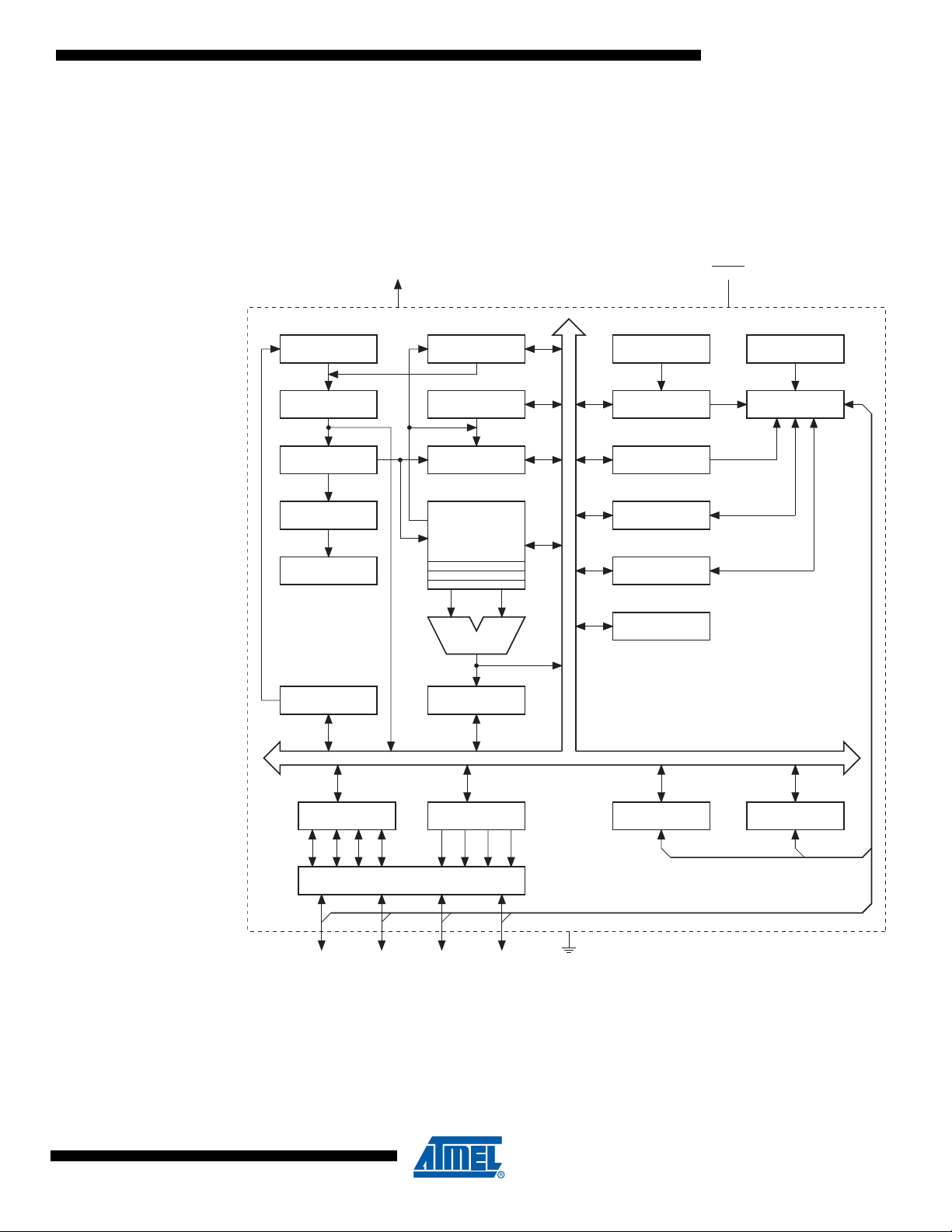
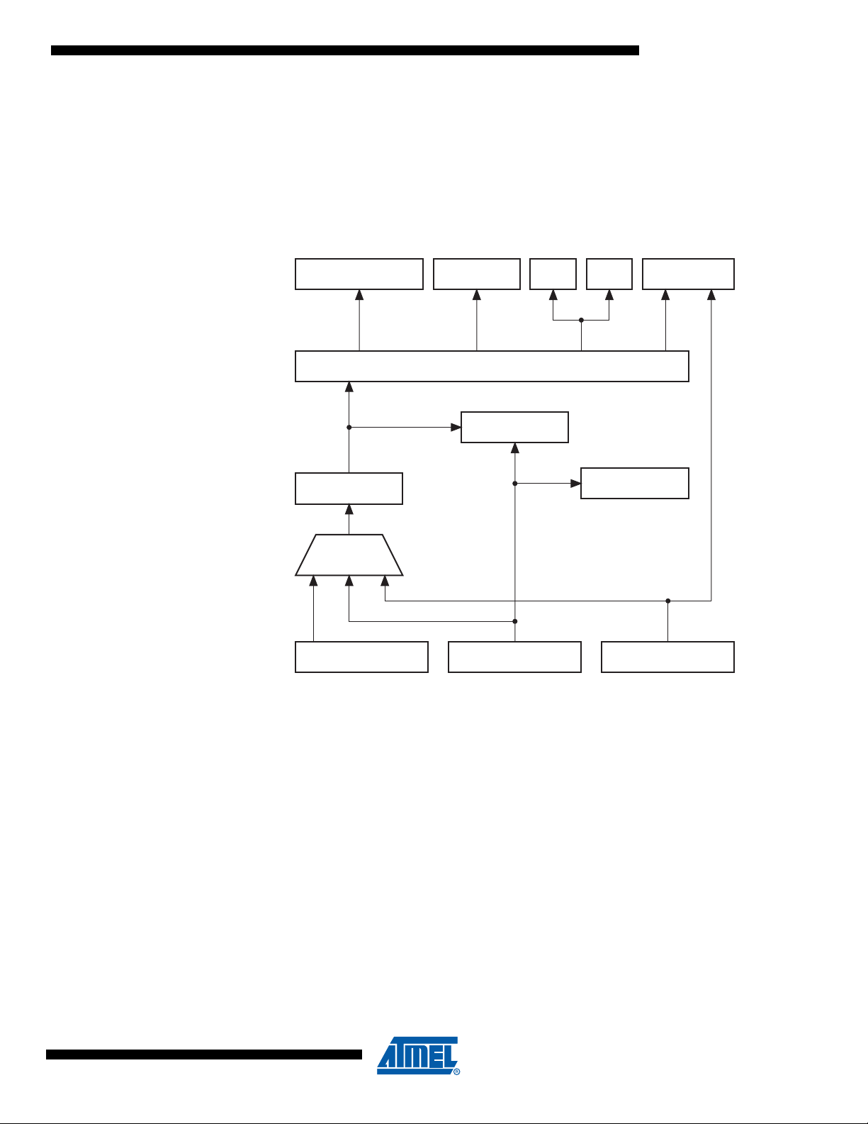
2. Overview
STACK
POINTER
SRAM
PROGRAM
COUNTER
PROGRAMMING
LOGIC
ISP
INTERFACE
INTERNAL
OSCILLATOR
WATCHDOG
TIMER
RESET FLAG
REGISTER
MCU STATUS
REGISTER
TIMER/
COUNTER0
CALIBRATED
OSCILLATOR
TIMING AND
CONTROL
INTERRUPT
UNIT
ANALOG
COMPARATOR
ADC
GENERAL
PURPOSE
REGISTERS
X
Y
Z
ALU
STATUS
REGISTER
PROGRAM
FLASH
INSTRUCTION
REGISTER
INSTRUCTION
DECODER
CONTROL
LINES
V
CC
RESET
DATA REGISTER
PORT B
DIRECTION
REG. PORT B
DRIVERS
PORT B
GND
PB3:0
8-BIT DATA BUS
ATtiny4/5/9/10
ATtiny4/5/9/10 are low-power CMOS 8-bit microcontrollers based on the compact AVR
enhanced RISC architecture. By executing powerful instructions in a single clock cycle, the
ATtiny4/5/9/10 achieve throughputs approaching 1 MIPS per MHz, allowing the system designer
to optimize power consumption versus processing speed.
Figure 2-1. Block Diagr am
8127B–AVR–08/09
The AVR core combines a rich instruction set with 16 general purpose working registers and
system registers. All registers are directly connected to the Arithmetic Lo gic Unit (ALU), allowing
two independent registers to be accessed in one single instruction executed in one clock cycle.
The resulting architecture is compact and code efficient while achieving throughputs up to ten
times faster than conventional CISC microcontrollers.
3
Page 4

ATtiny4/5/9/10
The ATtiny4/5/9/10 provide the following features: 512/1024 byte of In-System Programmable
Flash, 32 bytes of SRAM, four general purpose I/O lines, 16 general purpose working registers,
a 16-bit timer/counter with two PWM channels, internal and external interrupts, a programmable
watchdog timer with internal oscillator, an internal calibrated oscillator, and four software selectable power saving modes. ATtiny5/10 are also equipped with a four-channel, 8-bit Analog to
Digital Converter (ADC).
Idle mode stops the CPU while allowing the SRAM, timer/counter, ADC (ATtiny5/10 , only), ana log comparator, and interrupt system to continue functioning. ADC Noise Reduction mode
minimizes switching noise during ADC conversions by stopping the CPU and all I/O modules
except the ADC. In Power-down mode registers keep their contents and all chip functions are
disabled until the next interrupt or hardware reset. In Standby mode, the oscillator is running
while the rest of the device is sleeping, allowing very fast start-up combined with low power
consumption.
The device is manufactured using Atmel’s high density no n-volat ile mem ory tech nology. The onchip, in-system programmable Flash allows program memory to be re -programmed in- system by
a conventional, non-volatile memory prog ra m m er .
The ATtiny4/5/9/10 AVR are supported by a suite of program and system development tools,
including macro assemblers and evaluat ion k its.
2.1 Comparison of ATtiny4, ATtiny5, ATtiny9 and ATtiny10
A comparison of the devices is shown in Table 2-1.
Table 2-1. Differences between ATtiny4, ATtiny5, ATtiny9 and ATtiny10
Device Flash ADC Signature
ATtiny4 512 bytes No 0x1E 0x8F 0x0A
ATtiny5 512 bytes Yes 0x1E 0x8F 0x09
ATtiny9 1024 bytes No 0x1E 0x90 0x08
ATtiny10 1024 bytes Yes 0x1E 0x90 0x03
4
8127B–AVR–08/09
Page 5

3. General Information
3.1 Resources
A comprehensive set of drivers, application notes, data sheet s and descr iption s on development
tools are available for download at http://www.atmel.com/avr.
3.2 Code Examples
This documentation contains simple code examples t hat brief ly show h ow to us e various parts of
the device. These code examples assume that the part specific header file is included b efore
compilation. Be aware that not all C compiler vendors include bit definitions in the header files
and interrupt handling in C is compiler dependent . Please con firm wit h the C com piler d ocume ntation for more details.
3.3 Data Retention
Reliability Qualification results show that the projected data retention failure rate is much less
than 1 PPM over 20 years at 85°C or 100 years at 25°C.
3.4 Disclaimer
Typical values contained in this datasheet are based on simulations and characterization of
other AVR microcontrollers manufactured o n th e same proce ss te ch nolo gy. Min a nd Ma x valu es
will be available after the device has been characterized.
ATtiny4/5/9/10
8127B–AVR–08/09
5
Page 6
ATtiny4/5/9/10
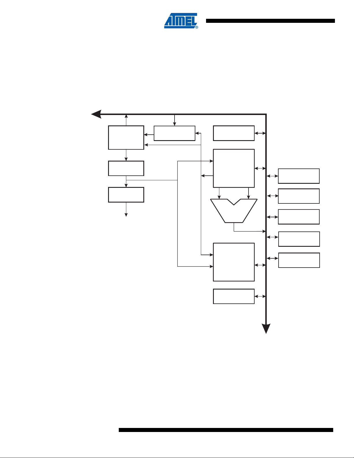
4. CPU Core
Data Bus 8-bit
This section discusses the AVR core architecture in general. The main function of the CPU core
is to ensure correct program execution. The CPU must therefore be able to access memories,
perform calculations, control peripherals, and handle interrupts.
4.1 Architectural Overview
Figure 4-1. Block Diagram of the AVR Architecture
Flash
Program
Memory
Instruction
Register
Instruction
Decoder
Control Lines
Program
Counter
Direct Addressing
Indirect Addressing
Status
and Control
16 x 8
General
Purpose
Registrers
ALU
Data
SRAM
I/O Lines
Interrupt
Unit
Watchdog
Tim er
Analog
Comparator
ADC
Timer/Counter 0
6
In order to maximize performance and parallelism, the AVR uses a Harvard architecture – with
separate memories and buses for program and data. Instructions in the program memory are
executed with a single level pipelining. While one instruction is being executed, the next instruction is pre-fetched from the program memory. This concept enables instructions to be executed
in every clock cycle. The program memory is In-System Reprogrammable Flash memory.
The fast-access Register File contains 16 x 8-bit general purpose working registers with a single
clock cycle access time. This allows single-cycle Arithmetic Logic Unit (ALU) operation. In a typical ALU operation, two operands are output from the Register File, the operation is executed,
and the result is stored back in the Register File – in one clock cycle.
8127B–AVR–08/09
Page 7

ATtiny4/5/9/10
Six of the 16 registers can be used as three 16-bit indirect address register pointers for data
space addressing – enabling efficient address calculations. One of the these address pointers
can also be used as an address pointe r for look up tables in Flash pr ogram memory. Thes e
added function registers are the 16-bit X-, Y-, and Z-register, described later in this section.
The ALU supports arithmetic and logic operations between registers or between a constant and
a register. Single register operations can also be executed in the AL U. After an arith metic operation, the Status Register is updated to reflect informat ion about the result of the operation.
Program flow is provided by conditional and unconditional jump and call instructions, capable of
directly addressing the whole address sp ace. Most AVR instruction s have a single 16-bit word
format but 32-bit wide instructions also exist. The actual instruction set varies, as some devices
only implement a part of the instruction set.
During interrupts and subroutine calls, the return address Prog ram Counter (PC) is stored on the
Stack. The Stack is effectively allocated in the general data SRAM, and consequently the Stack
size is only limited by the SRAM size and the usage of the SRAM. All user progra ms must initialize the SP in the Reset routine (before subroutines or interrupts are executed). The Stack
Pointer (SP) is read/write accessible in the I/O space. The data SRAM can easily be accessed
through the four different addressing modes supported in the AVR architecture.
The memory spaces in the AVR architecture are all linear and regular memory maps.
A flexible interrupt module has its control registers in the I/O space with an additional Global
Interrupt Enable bit in the Status Register. All interrupts have a separate Interrupt Vector in the
Interrupt Vector table. The interrupts have priority in accordance with their Interrupt Vector position. The lower the Interrupt Vector address, the higher the priority.
The I/O memory space contains 64 addresses for CPU peripheral functions as Control Registers, SPI, and other I/O functions. The I /O memory can be accesse d as the data sp ace locations,
0x0000 - 0x003F.
4.2 ALU – Arithmetic Logic Unit
The high-performance AVR ALU operates in direct connection with all the 16 general purpose
working registers. Within a single clock cycle, arithmetic operations between general purpose
registers or between a register and an immediate are execut ed . The ALU ope ra tio ns are divided
into three main categories – arithmetic, logical, and bit-functions. Some implementations of the
architecture also provide a powerful multiplier supporting both signed/unsigned multiplication
and fractional format. See document “AVR Instruction Set” and section “Instruction Set Sum-
mary” on page 151 for a detailed description.
4.3 Status Register
The Status Register contains information abou t th e result o f th e most r ecently exe cuted arith metic instruction. This information can be used for altering program flow in order to perform
conditional operations. Note that the Status Register is updated after all ALU operations, as
specified in document “AVR Instruction Set” and section “Instruction Se t Summary” on page
151. This will in many cases remove the need for using the dedicated compare instructions,
resulting in faster and more compact code.
8127B–AVR–08/09
The Status Register is not automatically stored when entering an interrupt routine and restored
when returning from an interrupt. This must be hand le d by so ftware.
7
Page 8

ATtiny4/5/9/10
4.4 General Purpose Register File
The Register File is optimized for the AVR Enhanced RISC instruction set. In order t o achieve
the required performance and flexibility, the following input/output schemes are supported by the
Register File:
• One 8-bit output operand and one 8-bit result input
• Two 8-bit output operands and one 8-bit result input
• One 16-bit output ope rand and one 16-bit result input
Figure 4-2 below shows the structure of the 16 general purpose working registe rs in the CPU.
Figure 4-2. AVR CPU General Purpose Working Registers
General R18
Purpose …
Working R26 X-register Low Byte
Registers R27 X-register High Byte
70
R16
R17
R28 Y-register Low Byte
Note: A typical implementation of the AVR register file includes 32 general prupose registers but
ATtiny4/5/9/10 implement only 16 registers. For reasons of compatibility the registers are numbered R16...R31, not R0...R15.
Most of the instructions operating on the Register File have direct access to all registers, and
most of them are single cycle instructions.
4.4.1 The X-register, Y-register, and Z-register
Registers R26..R31 have some added fu nctions to their gene ral purpose usage . These regist ers
are 16-bit address pointers for indirect addressing of the data space. The three indirect address
registers X, Y, and Z are defined as described in Figure 4-3.
R29 Y-register High Byte
R30 Z-register Low Byte
R31 Z-register High Byte
8
8127B–AVR–08/09
Page 9

ATtiny4/5/9/10
Figure 4-3. The X-, Y-, and Z-registers
15 XH XL 0
X-register 707 0
R27 R26
15 YH YL 0
Y-register 707 0
R29 R28
15 ZH ZL 0
Z-register 707 0
R31 R30
In different addressing modes these address registers function as automatic increment and
automatic decrement (see document “AVR Instruction Set” and section “Instruction Set Sum-
mary” on page 151 for details).
4.5 Stack Pointer
The Stack is mainly used for storing temporary data, for storing local variables and for storing
return addresses after interrupts and subroutine calls. The Stack Pointer Register always points
to the top of the Stack. Note that the Stack is imp lemented as growing f rom higher memor y locations to lower memory locations. This implies that a Stack PUSH co mmand decr eases th e Stack
Pointer.
The Stack Pointer points to the data SRAM Stack area where the Subroutine and Interrupt
Stacks are located. This Stack space in the data SRAM must be defined by the program before
any subroutine calls are executed or interrupts are enabled. The Stack Pointer must be set to
point above 0x40. The Stack Pointer is decremented by one when dat a is pushed onto the Stack
with the PUSH instruction, and it is decremented by two when the return address is pushed onto
the Stack with subroutine call or interrupt. The Stack Pointer is increment ed by one when dat a is
popped from the Stack with the POP instruction, and it is incremented by two when data is
popped from the Stack with return from subroutine RET or return from interrupt RETI.
The AVR Stack Pointer is implemented as two 8-bit registers in the I/O space. The number of
bits actually used is implementation dependent. Note that the data space in some implementations of the AVR architecture is so small that only SPL is needed. In this case, the SPH Register
will not be present.
4.6 Instruction Execution Timing
This section describes the general access timing concepts for instruction execution. The AVR
CPU is driven by the CPU clock clk
chip. No internal clock division is used.
, directly generated from the selected clock source for the
CPU
8127B–AVR–08/09
9
Page 10
ATtiny4/5/9/10
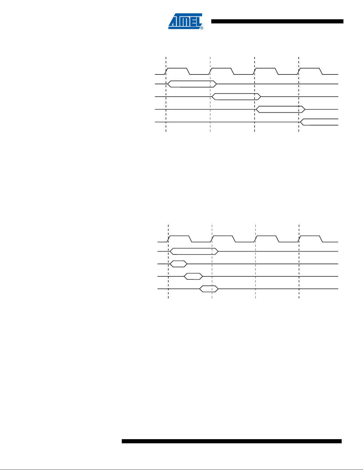
Figure 4-4. The Parallel Instruction Fetches and Instruction Executions
clk
1st Instruction Fetch
1st Instruction Execute
2nd Instruction Fetch
2nd Instruction Execute
3rd Instruction Fetch
3rd Instruction Execute
4th Instruction Fetch
T1 T2 T3 T4
CPU
Total Execution Time
Register Operands Fetch
ALU Operation Execute
Result Write Back
T1 T2 T3 T4
clk
CPU
Figure 4-4 shows the parallel instruction fetches and instruction executions enabled by the Har-
vard architecture and the fast access Register File concept. This is the basic pipelining concept
to obtain up to 1 MIPS per MHz with the corresponding unique results for functions per cost,
functions per clocks, and functions per power-unit.
Figure 4-5 shows the internal timing concept for th e Regi ster File. I n a single clock cycl e an ALU
operation using two register operands is executed, and the result is stored back to the destination register.
Figure 4-5. Single Cycle ALU Operation
4.7 Reset and Interrupt Handling
10
The AVR provides several different interrupt sources. These interrupts and the separate Reset
Vector each have a separate Program Vector in the program memory spa ce. All interrupts are
assigned individual enable bits which must be written logic one toge ther with the Glo bal Interru pt
Enable bit in the Status Register in order to enable the int errupt.
The lowest addresses in the program memory space are by default defined as the Reset and
Interrupt Vectors. The complete list of vectors is shown in “Interrupts” on page 35. The list also
determines the priority levels of the different interrupts. The lower the address the higher is the
priority level. RESET has the highest priority, and next is INT0 – the External Interrupt Request
0.
When an interrupt occurs, the Global Interrupt Enable I-bit is cleared and all interrupts are dis-
abled. The user software can write logic one to the I-bit to enable nested interrupts. All enabled
8127B–AVR–08/09
Page 11

ATtiny4/5/9/10
interrupts can then interrupt the current interrupt routine. The I-bit is automatically set when a
Return from Interrupt instruction – RETI – is executed.
There are basically two types of interrupts. The first type is triggered by an event that sets the
Interrupt Flag. For these interrupts, the Program Counter is vectored to the actual Interrupt Vector in order to execute the interrupt handling routine, and hardware clears the corresponding
Interrupt Flag. Interrupt Flags can also be cleared by writing a logic one to the fl ag bit position(s)
to be cleared. If an interrupt condition occurs while the corresponding interrupt enable bit is
cleared, the Interrupt Flag will be set and remembered until the interrupt is enabled, or the flag is
cleared by software. Similarly, if one or more interrupt conditions occur while the Global Interrupt
Enable bit is cleared, the corresponding Interrupt Flag(s) will be set and remembered until the
Global Interrupt Enable bit is set, and will then be executed by order of priority.
The second type of interrupts will trigger as long as the interrupt condition is present. These
interrupts do not necessarily have Int errupt Flags. If the interrup t condition disappears before t he
interrupt is enabled, the interrupt will not be triggered.
When the AVR exits from an interrupt, it will always return to the main program and execute one
more instruction before any pending interrupt is served.
Note that the Status Register is not automatically stored when entering an interrupt routine, nor
restored when returning from an interrupt rou tine. This must be handled by software.
When using the CLI instruction to disable interrupts, the interrupts will be immediately disabled.
No interrupt will be executed after the CLI instruction, even if it occurs simultaneously with the
CLI instruction.
When using the SEI instruction to enable interrupts, the instruction following SEI will be executed before any pending interrupts, as shown in the following example.
Assembly Code Example
sei ; set Global Interrupt Enable
sleep ; enter sleep, waiting for interrupt
Note: See “Code Examples” on page 5.
4.7.1 Interrupt Response Time
The interrupt execution response for all the enabled AVR interrupts is four clock cycles minimum. After four clock cycles the Program Vector address for the a ctual interru pt handling routine
is executed. During this four clock cycle period, the Program Counter is pushed onto the Stack.
The vector is normally a jump to the interrupt routine, and this jump takes three clock cycles. If
an interrupt occurs during execution of a multi-cycle instruction, this instruction is completed
before the interrupt is served. If an interrupt occurs when the MCU is in sleep mode, the interrupt
execution response time is increased by four clock cycles. This increase comes in ad dition to the
start-up time from the selected sleep mode.
; note: will enter sleep before any pending interrupt(s)
8127B–AVR–08/09
A return from an interrupt handling routine takes four clock cycles. During these four clock
cycles, the Program Counter (two bytes) is popped back from the Stack, the Stack Pointer is
incremented by two, and the I-bit in SREG is set.
11
Page 12
ATtiny4/5/9/10
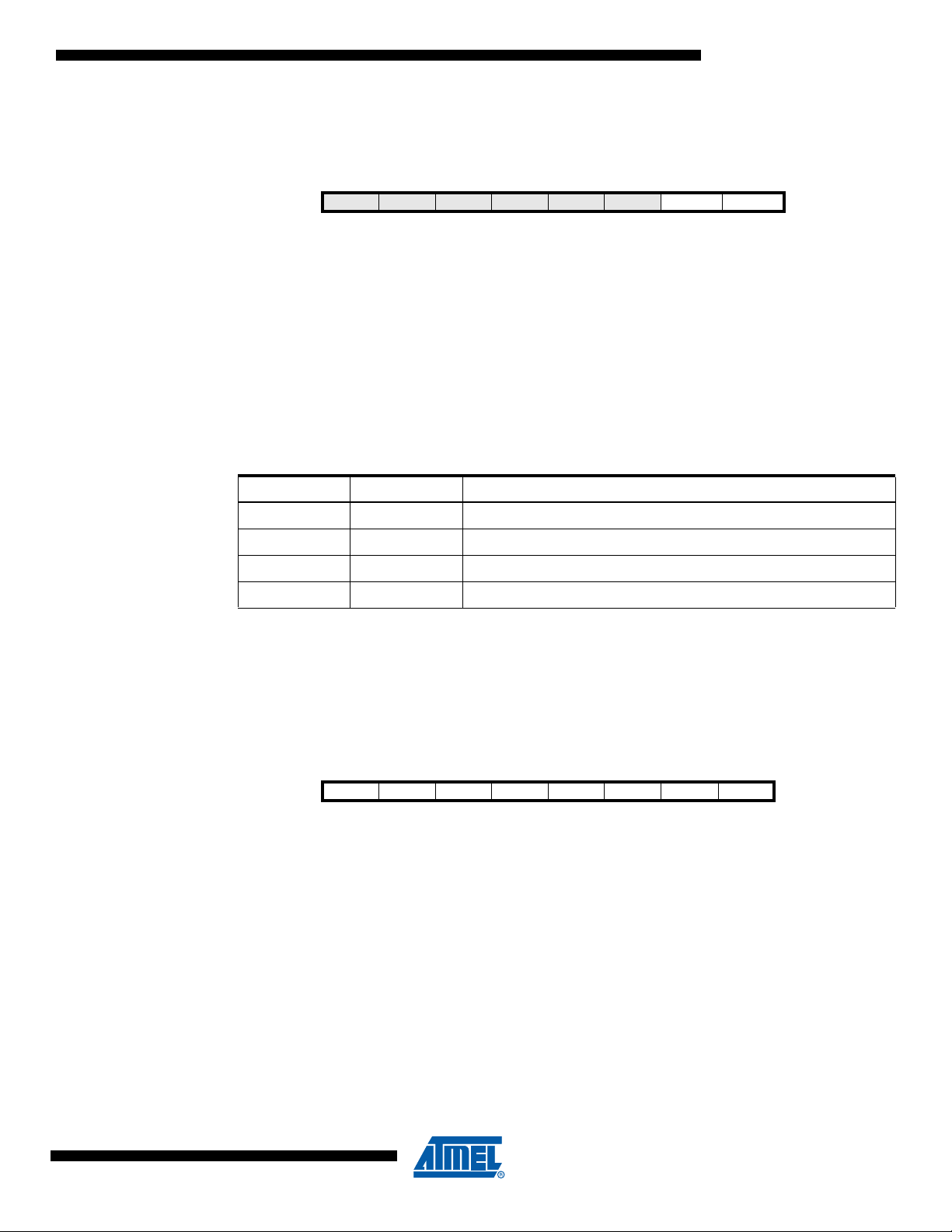
4.8 Register Description
4.8.1 CCP – Configuration Change Protection Register
Bit 76543210
0x3C CCP[7:0] CCP
Read/WriteWWWWWWWW
Initial Value00000000
• Bits 7:0 – CCP[7:0] – Configuration Change Protection
In order to change the contents of a protected I/O register the CCP register must first be written
with the correct signature. After CCP is written the protected I/O registers may be written to during the next four CPU instruction cycles. All interrupts are ignored during these cycles. After
these cycles interrupts are automatically handled again by the CPU, and any pending interrupts
will be executed according to their priority.
When the protected I/O register signature is written, CCP[0] will read as one as long as the protected feature is enabled, while CCP[7:1] will always read as zero.
Table 4-1 shows the signatures that are in recognised.
Table 4-1. Signatures Recognised by the Configuration Change Protection Register
Signature Group Description
0xD8 IOREG: CLKMSR, CLKPSR, WDTCSR Protected I/O register
4.8.2 SPH and SPL — Stack Pointer Register
Bit 151413121110 9 8
0x3E SP15 SP14 SP13 SP12 SP11 SP10 SP9 SP8 SPH
0x3D SP7 SP6 SP5 SP4 SP3 SP2 SP1 SP0 SPL
76543210
Read/Write R/W R/W R/W R/W R/W R/W R/W R/W
Read/Write R/W R/W R/W R/W R/W R/W R/W R/W
Initial Value
Initial Value
RAMEND RAMEND RAMEND RAMEND RAMEND RAMEND RAMEND RAMEND
RAMEND RAMEND RAMEND RAMEND RAMEND RAMEND RAMEND RAMEND
4.8.3 SREG – Status Register
Bit 76543210
0x3F I T H S V N Z C SREG
Read/Write R/W R/W R/W R/W R/W R/W R/W R/W
Initial Value00000000
• Bit 7 – I: Global Interrupt Enable
The Global Interrupt Enable bit must be set for the interrupts to be enabled. The individual interrupt enable control is then performed in separate control registers. If the Global Interrupt Enable
Register is cleared, none of the interrupts are enabled independent of the individual interrupt
enable settings. The I-bit is cleared by hardware after an interrupt has occurred, and is set by
the RETI instruction to enable subsequent interrupts. The I-bit can also be set and cleared by
the application with the SEI and CLI instructions, as described in the document “AVR Instruction
Set” and “Instruction Set Summary” on page 151.
12
• Bit 6 – T: Bit Copy Storage
8127B–AVR–08/09
Page 13

ATtiny4/5/9/10
The Bit Copy instructions BLD (Bit LoaD) and BST (Bit STore) use the T-bit as source or destination for the operated bit. A bit from a register in the Register File can be copied into T by the
BST instruction, and a bit in T can be copied into a bit in a register in the Register File by the
BLD instruction.
• Bit 5 – H: Half Carry Flag
The Half Carry Flag H indicates a Half Carry in some arithmetic operations. Half Carry is useful
in BCD arithmetic. See document “AVR Instruction Set” and section “Instruction Set Summary”
on page 151 for detailed informatio n.
• Bit 4 – S: Sign Bit, S = N
The S-bit is always an exclusive or between the Negative Flag N and the Two’s Complement
Overflow Flag V. See document “AVR Instruction Set” and section “Instruction Set Summary” on
page 151 for detailed information.
• Bit 3 – V: Two’s Comple ment Overflow Flag
The Two’s Complement Overflow Flag V supports two’s complement arithmet ics. See d ocument
“AVR Instruction Set” and section “Instruction Set Summary” on page 151 for detailed
information.
• Bit 2 – N: Negative Flag
The Negative Flag N indicates a negative result in an arithmetic or logic operation. See document “AVR Instruction Set” and section “Instruction Set Summary” on page 151 for detailed
information.
• Bit 1 – Z: Zero Flag
The Zero Flag Z indicates a zero result in an arithmetic or logic operation. See document “AVR
Instruction Set” and section “Instruction Set Summary” on page 151 for detailed information.
• Bit 0 – C: Carry Flag
The Carry Flag C indicates a carry in an arithmetic or logic operation. See document “AVR
Instruction Set” and section “Instruction Set Summary” on page 151 for detailed information.
⊕ V
8127B–AVR–08/09
13
Page 14

ATtiny4/5/9/10
5. Memories
This section describes the different memories in the AT tiny4/5/9/10. Devices have two ma in
memory areas, the program memory space and the data memory space.
5.1 In-System Re-programmable Flash Program Memory
The ATtiny4/5/9/10 contain 512/1024 bytes of on-chip, in-system reprogrammable Flash memory for program storage. Since all AVR instructions are 16 or 32 bits wide, the Flash is organized
as 256/512 x 16.
The Flash memory has an endurance of at least 10,000 write/erase cycles. The ATtiny4/5/9/10
Program Counter (PC) is 9 bits wide, thus capable of addressing the 256/512 program memory
locations, starting at 0x000. “Memory Progr amming” on page 107 cont ains a detailed d escription
on Flash data serial downloading.
Constant tables can be allocated within the entire addre ss space of program memo ry. Since program memory can not be accessed directly, it has been mapped to the data memory. The
mapped program memory begins at byte address 0x 4000 in data memory (see Figure 5-1 on
page 15). Although programs are executed starting from address 0x000 in program memory it
must be addressed starting from 0x4000 when accessed via the data memory.
Internal write operations to Flash program memory have been disabled and program memory
therefore appears to firmware as read-only. Flash memory can still be written to externally but
internal write operations to the program memory area will not be succesful.
5.2 Data Memory
Timing diagrams of instruction fetch and execution are presented in “Instruction Execution Tim-
ing” on page 9.
Data memory locations include the I/O memory, the internal SRAM memory, the non-volatile
memory lock bits, and the Flash memory. See Figure 5-1 on page 15 for an illustration on how
the ATtiny4/5/9/10 memory space is organized.
The first 64 locations are reserved for I/O memo ry, while th e follo win g 32 d ata m emory loca tio ns
address the internal data SRAM.
The non-volatile memory lock bits and all the Flash memory sections are ma pped to the data
memory space. These locations appear as read-only for device firmware.
The four different addressing modes for data me mory are dire ct, indirect, in direct with pre- decrement, and indirect with post-increment. In the register file, registers R26 to R31 function as
pointer registers for indirect addressing.
The IN and OUT instructions can access all 64 locations of I/O mem ory. Dire ct a dd ressing using
the LDS and STS instructions reaches the 128 locations between 0 x0040 and 0x00BF.
The indirect addressing reaches the entire data memory space. When using indirect addressing
modes with automatic pre-decrement and post-increment, the address registers X, Y, and Z are
decremented or incremented.
14
8127B–AVR–08/09
Page 15
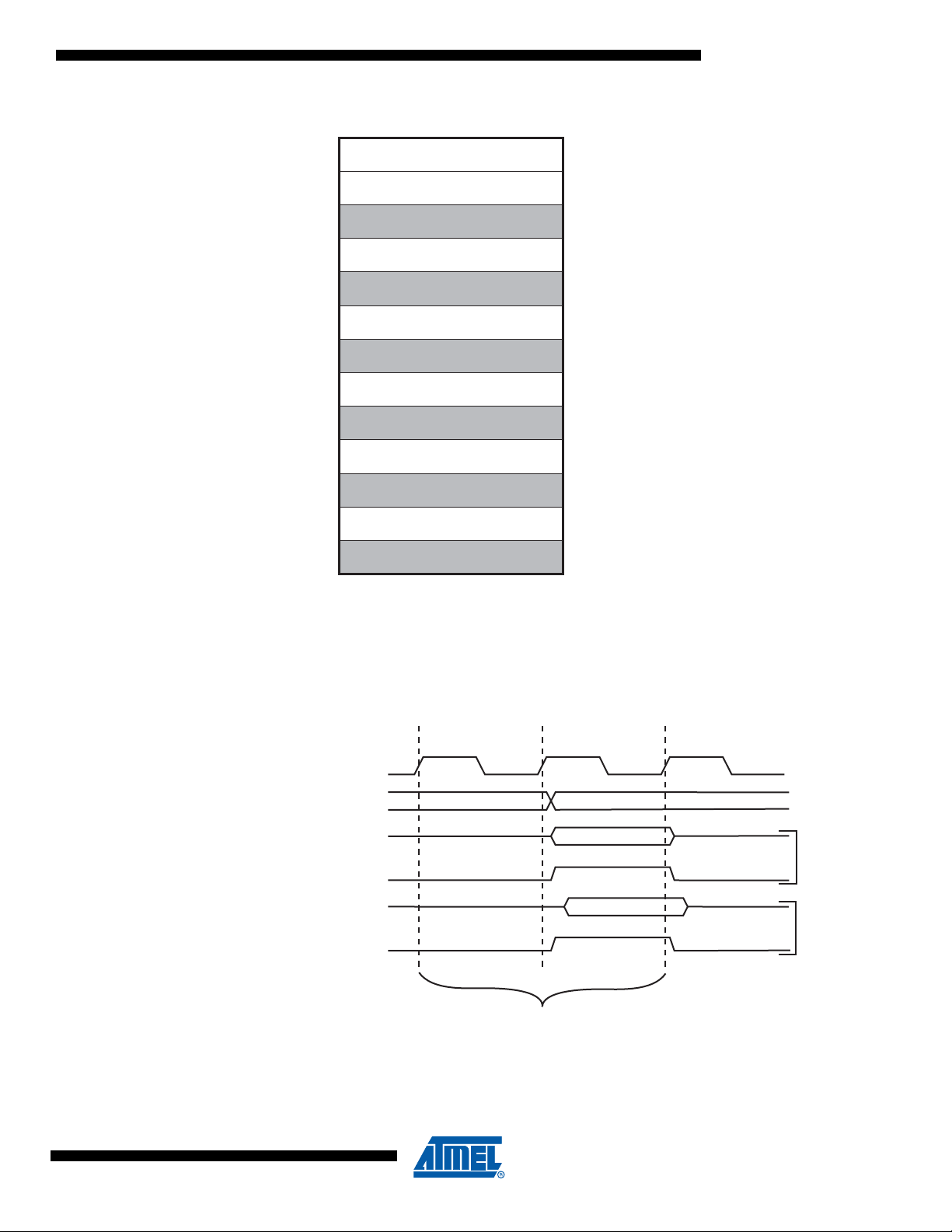
Figure 5-1. Data Memory Map (Byte Addressing)
0x0000 ... 0x003F
0x0040 ... 0x005F
0x0060 ... 0x3EFF
0x3F00 ... 0x3F01
0x3F02 ... 0x3F3F
0x3F40 ... 0x3F41
0x3F42 ... 0x3F7F
0x3F80 ... 0x3F81
0x3F82 ... 0x3FBF
0x3FC0 ... 0x3FC3
0x3FC4 ... 0x3FFF
0x4000 ... 0x41FF/0x43FF
0x4400 ... 0xFFFF
I/O SPACE
SRAM DATA MEMORY
(reserved)
NVM LOCK BITS
(reserved)
CONFIGURATION BITS
(reserved)
CALIBRATION BITS
(reserved)
DEVICE ID BITS
(reserved)
FLASH PROGRAM MEMORY
(reserved)
clk
WR
RD
Data
Data
Address
Address valid
T1 T2 T3
Compute Address
Read
Write
CPU
Memory Access Instruction
Next Instruction
ATtiny4/5/9/10
5.2.1 Data Memory Access Times
5.3 I/O Memory
8127B–AVR–08/09
This section describes the general access timing concepts for internal memory access. The
internal data SRAM access is performed in two clk
cycles as described in Figure 5-2.
CPU
Figure 5-2. On-chip Data SRAM Access Cycles
The I/O space definition of the ATtiny4/5/9/ 10 is shown in “Register Summary” on page 149.
15
Page 16

ATtiny4/5/9/10
All ATtiny4/5/9/10 I/Os and peripherals are placed in the I/O space. All I/O locations may be
accessed using the LD and ST instructions, enabling data transfer between the 16 general purpose working registers and the I/O space. I/O Registers within the address range 0x00 - 0x1F
are directly bit-accessible using the SBI and CBI instructions. In these r egister s, the value o f single bits can be checked by using the SBIS and SBIC instructions. See document “AVR
Instruction Set” and section “Instruction Set Summary” on page 151 for more details. When
using the I/O specific commands IN and OUT, the I/O addresses 0x00 - 0x3F must be used.
For compatibility with future devices, reserved bits should be written to zero if accessed.
Reserved I/O memory addresses should never be written.
Some of the status flags are cleared by writing a logical one to them. Note that CBI and SBI
instructions will only operate on the specified bit, and can therefore be used on registers containing such status flags. The CBI and SBI instructions work on registers in the address range 0x00
to 0x1F, only.
The I/O and Peripherals Control Registers are explained in later sections.
16
8127B–AVR–08/09
Page 17
6. Clock System
ATtiny4/5/9/10
Figure 6-1 presents the principal clock systems and their distribution in ATtiny4/5/9/10. All of the
clocks need not be active at a given time. In order to reduce power consumption, the clocks to
modules not being used can be halted by using different sleep modes and power reduction register bits, as described in “Power Management and Sleep Modes” o n page 23. The clock
systems is detailed below.
Figure 6-1. Clock Distribution
ANALOG-TO-DIGITAL
CONVERTER
GENERAL
I/O MODULES
CPU
CORE
RAM
NVM
6.1 Clock Subsystems
The clock subsystems are detailed in the sections below.
clk
SOURCE CLOCK
CLOCK
PRESCALER
CLOCK
SWITCH
EXTERNAL
CLOCK
ADC
clk
I/O
CLOCK CONTROL UNIT
RESET
LOGIC
WATCHDOG
CLOCK
WATCHDOG
OSCILLATOR
clk
CPU
WATCHDOG
TIMER
clk
NVM
CALIBRATED
OSCILLATOR
6.1.1 CPU Clock – clk
6.1.2 I/O Clock – clk
6.1.3 NVM clock - clk
8127B–AVR–08/09
CPU
The CPU clock is routed to parts of the system concerned with operation of the AVR Core.
Examples of such modules are the General Purpose Register File, the System Registers and
the SRAM data memory. Halting the CPU clock inhibits the core from performing general operations and calculations.
I/O
The I/O clock is used by the majority o f the I/O modules, like T imer/Counter. The I/O clock is
also used by the External Interrupt module, but note that some external interrupts are detected
by asynchronous logic, allowing such interrupts to be detected even if the I/O clock is halted.
NVM
The NVM clock controls operation of the Non-Volatile Memory Controller. The NVM clock is usually active simultaneously with the CPU clock.
17
Page 18

ATtiny4/5/9/10
6.1.4 ADC Clock – clk
EXTERNAL
CLOCK
SIGNAL
CLKI
GND
ADC
The ADC is provided with a dedicated clock domain. This allows halting the CPU and I/O clocks
in order to reduce noise generated by digital cir cuit ry. Th is gives mo re accurat e ADC conversion
results.
The ADC is available in ATtiny5/10, only.
6.2 Clock Sources
All synchronous clock signals are der ived from th e main clock. T he device ha s three alt ernative
sources for the main clock, as follows:
• Calibrated Internal 8 MHz Oscillator (see page 18)
• External Clock (see page 18)
• Internal 128 kHz Oscillator (see page 19)
See Table 6-3 on page 21 on how to select and chang e the active clock source.
6.2.1 Calibrated Internal 8 MHz Oscillator
The calibrated internal oscillator provides an approximately 8 MHz clock signal. Though voltage
and temperature dependent, this clock can be very accurately calibrated by the user. See Table
16-2 on page 118, Figure 17-39 on page 142 and Figur e 17-40 on page 142 for more details.
This clock may be selected as the main clock by setting the Clock Main Select bits CLKMS[1:0]
in CLKMSR to 0b00. Once enabled, the oscillator will operate with no external components. During reset, hardware loads the calibration byte into the OSCCAL register and thereby
automatically calibrates the oscillator. The accuracy of this calibration is shown as Factory calibration in Table 16-2 on page 118.
6.2.2 External Clock
When this oscillator is used as the main clock, the watchdog oscillator will still be used for the
watchdog timer and reset time-out. For more information on the pre-programmed calibration
value, see section “Calibration Section” on page 110.
To use the device with an external clock source, CLKI should be driven as shown in Figure 6-2.
The external clock is selected as the main clock by setting CLKMS[1:0] bits in CLKMSR to 0b10.
Figure 6-2. External Clock Drive Configuration
When applying an external clock, it is required to avoid sudden changes in the applied clock frequency to ensure stable operation of the MCU. A variation in frequency of more than 2% from
one clock cycle to the next can lead to unpredictable behavior. It is required to ensure that the
MCU is kept in reset during such changes in the clock frequency.
18
8127B–AVR–08/09
Page 19

6.2.3 Internal 128 kHz Oscillator
The internal 128 kHz oscillator is a low power oscillator providing a clock of 128 kHz. The frequency depends on supply voltage, temperature and batch variations. This clock may be select
as the main clock by setting the CLKMS[1:0] bits in CLKMSR to 0b01.
6.2.4 Switching Clock Source
The main clock source can be switched at run-time using the “CLKMSR – Clock Main Settings
Register” on page 21. When switching between any clock sources, the clock system ensures
that no glitch occurs in the main clock.
6.2.5 Default Clock Source
The calibrated internal 8 MHz oscillator is always selected as main clock when the device is
powered up or has been reset. The synchronous system clock is the main clock divided by 8,
controlled by the System Clock Prescaler. The Clock Prescaler Select Bits can be written later to
change the system clock frequency. See “System Clock Prescaler”.
6.3 System Clock Prescaler
The system clock is derived from the main clock via the System Clock Prescaler. The system
clock can be divided by setting the “CLKPSR – Clock Prescale Register” on page 22. The sys-
tem clock prescaler can be used to decrease power consumption at times when requirements
for processing power is low or to bring the system clock wit hin limits of maximum f requency. The
prescaler can be used with all main clock source options, and it will affect the clock frequency of
the CPU and all synchronous peripherals.
ATtiny4/5/9/10
The System Clock Prescaler can be used to implement run-time changes of the internal clock
frequency while still ensuring stable operation.
6.3.1 Switching Prescaler Setting
When switching between prescaler settings, the system clock prescaler ensures that no glitch
occurs in the system clock and that no intermediate frequency is higher than neither the clock
frequency corresponding the previous setting, nor the clock frequency corresponding to the new
setting.
The ripple counter that implements the prescaler runs at the frequency of the main clock, which
may be faster than the CPU's clock frequency. Hence, it is not possible to determine the state of
the prescaler - even if it were readable, and the exact time it takes to switch from one clock division to another cannot be exactly predicted.
From the time the CLKPS values are written, it takes between T1 + T2 and T1 + 2*T2 before the
new clock frequency is active. In this interval, two active clock edges are produced. Here, T1 is
the previous clock period, and T2 is the period corresponding to the new prescaler setting.
8127B–AVR–08/09
19
Page 20

ATtiny4/5/9/10
6.4 Starting
6.4.1 Starting from Reset
The internal reset is immediately asserted when a rese t so urce go es acti ve. The int erna l r eset is
kept asserted until the reset source is released and the start-up sequence is completed. The
start-up sequence includes three steps, as follows.
1. The first step after the reset source has been released consists of the device counting
2. The second step is to count the oscillator start-up time, which ensures that the cali-
3. The last step before releasing t he internal reset is to load the calibr at ion and t he conf ig-
the reset start-up time. The purpose of this reset start-up time is to ensure that supply
voltage has reached sufficient levels. The reset start-up time is counted using the internal 128 kHz oscillator. See Table 6-1 for details of reset start-up time.
Note that the actual supply voltage is not mon itored by the start-up logic. The device
will count until the reset start-up time has elapsed even if the device has reached sufficient supply voltage levels earlier.
brated internal oscillator has reached a stable state before it is used by the other parts
of the system. The calibrated internal oscillator needs to oscillate for a minimum number of cycles before it can be considered sta ble. See Table 6-1 for details of the
oscillator start-up time.
uration values from the Non-Volatile Memory to configure the device properly. The
configuration time is listed in Table 6-1.
Table 6-1. Start-up Times when Using the Internal Calibrated Oscillator
Reset Oscillator Configuration Total start-up time
64 ms 6 cycles 21 cycles 64 ms + 6 oscillator cycles + 21 system clock cycles
Notes: 1. After powering up the device or after a reset the system clock is automatically set to calibrated
internal 8 MHz oscillator, divided by 8
6.4.2 Starting from Power-Down Mode
When waking up from Power-Down sleep mode, the supply voltage is assumed to be at a sufficient level and only the oscillator start-up time is counted to ensure the stable operation of the
oscillator. The oscillator start-up time is counted on the selected main clock, and the start-up
time depends on the clock selected. See Table 6-2 for details.
Table 6-2. Start-up Time from Power-Down Sleep Mode.
Oscillator start-up time Total start-up time
6 cycles 6 oscillator cycles
Notes: 1. The start-up time is measured in main clock oscillator cycles.
6.4.3 Starting from Idle / ADC Noise Reduction / Standby Mode
When waking up from Idle, ADC Noise Reduction or Standby Mode, the oscillator is already running and no oscillator start-up time is introduced.
(1)
(1)
20
The ADC is available in ATtiny5/10, only.
8127B–AVR–08/09
Page 21
6.5 Register Description
6.5.1 CLKMSR – Clock Main Settings Register
Bit 765432 1 0
0x37
Read/WriteRRRRRRR/WR/W
Initial Value 0 0 0 0 0 0 0 0
• Bit 7:2 – Res: Reserved Bits
These bits are reserved and always read zero.
• Bit 1:0 – CLKMS[1:0]: Clock Main Select Bits
These bits select the main clock source of the system. The bits can be written at run-time to
switch the source of the main clock. The clock system ensures glitch free switching of the main
clock source.
The main clock alternatives are shown in Table 6-3.
Table 6-3. Selection of Main Clock
CLKM1 CLKM0 Main Clock Source
0 0 Calibrated Internal 8 MHzOscillator
– – – – – – CLKMS1 CLKMS0 CLKMSR
ATtiny4/5/9/10
0 1 Internal 128 kHz Oscillator (WDT Oscillator)
1 0 External clock
11Reserved
To avoid unintentional switching of main clock source, a protected change se quence must be
followed to change the CLKMS bits, as follows:
1. Write the signature for change enable of protected I/O register to register CCP
2. Within four instruction cycles, write the CLKMS bits with the desired value
6.5.2 OSCCAL – Oscillator Calibration Register
.
Bit 76543210
0x39 CAL7 CAL6 CAL5 CAL4 CAL3 CAL2 CAL1 CAL0 OSCCAL
Read/Write R/W R/W R/W R/W R/W R/W R/W R/W
Initial Value 0 0 0 0 0 0 0 0
• Bits 7:0 – CAL[7:0]: Oscillator Calibration Value
The oscillator calibration register is used to trim the calibrated internal oscillator and remove process variations from the oscillator frequency. A pre-programmed calibration value is
automatically written to this register during chip reset, giving the factory calibrated frequency as
specified in Table 16-2, “Calibration Accuracy of Internal RC Oscillator,” on page 118.
The application software can write this register to change the oscillator frequency. The oscillator
can be calibrated to frequencies as specified in Table 16-2, “Calibration Accuracy of Internal RC
Oscillator,” on page 118. Calibration outside the range given is not guaranteed.
8127B–AVR–08/09
The CAL[7:0] bits are used to tune the frequency of the oscillator. A setting of 0x00 gives the
lowest frequency, and a setting of 0xFF gives the highest frequency.
21
Page 22

ATtiny4/5/9/10
6.5.3 CLKPSR – Clock Prescale Register
Bit 76543210
0x36
Read/Write R R R R R/W R/W R/W R/W
Initial Value00000011
– – – – CLKPS3 CLKPS2 CLKPS1 CLKPS0 CLKPSR
• Bits 7:4 – Res: Reserved Bits
These bits are reserved and will always read as zero.
• Bits 3:0 – CLKPS[3:0]: Clock Prescaler Select Bits 3 - 0
These bits define the division factor between the selected clock source and the internal system
clock. These bits can be written at run-time to vary the clock frequency and suit the application
requirements. As the prescaler divides the master clock input to the MCU, the spee d of all synchronous peripherals is reduced accordingly. The division factors are given in Table 6-4.
Table 6-4. Clock Prescaler Select
CLKPS3 CLKPS2 CLKPS1 CLKPS0 Clock Division Factor
0000 1
0001 2
0010 4
0 0 1 1 8 (default)
0100 16
0101 32
0110 64
0111 128
1000 256
1001 Reserved
1010 Reserved
1011 Reserved
1100 Reserved
1101 Reserved
1110 Reserved
1111 Reserved
To avoid unintentional changes of clock frequency, a protected change sequence must be followed to change the CLKPS bits:
1. Write the signature for change enable of protected I/O register to register CCP
2. Within four instruction cycles, write the desired value to CLKPS bits
At start-up, CLKPS bits are reset to 0 b0011 to select t he clock division fact or of 8. If the select ed
clock source has a frequency higher than the maximum allowed the application software must
make sure a sufficient division factor is used. To make sure the write procedure is not interrupted, interrupts must be disabled when changing prescale r settings.
22
8127B–AVR–08/09
Page 23

7. Power Management and Sleep Modes
The high performance and industry leading code efficiency makes the AVR microcontrollers an
ideal choise for low power applications. In addition, sleep modes enable the application to shut
down unused modules in the MCU, thereby saving power. The AVR provides various sleep
modes allowing the user to tailor the power consumption to the application’s requirements.
7.1 Sleep Modes
Figure 6-1 on page 17 presents the different clock systems and their distribution in
ATtiny4/5/9/10. The figure is helpful in selecting an appropriate sleep mode. Table 7-1 shows
the different sleep modes and their wake up sources.
Table 7-1. Active Clock Domains and Wake-up Sources in Different Sleep Modes
Active Clock Domains Oscillators Wake-up Sources
Sleep Mode
Idle XX X XXXXX
ADC Noise Reduction X X X
Standby X X
Power-down X
CPU
clk
NVM
clk
(1)
ADC
clkIOclk
ATtiny4/5/9/10
(1)
Main Clock
Source Enabled
INT0 and
Pin Change
ADC
Other I/O
Watchdog
Interrupt
(2)
XXX
(2)
(2)
X
X
VLM Interrupt
7.1.1 Idle Mode
Note: 1. The ADC is available in ATtiny5/10, only
2. For INT0, only level interrupt.
To enter any of the four sleep modes, the SE bits in SMCR must be written to logic one and a
SLEEP instruction must be executed. The SM2:0 bits in the SMCR register select which sleep
mode (Idle, ADC Noise Reduction, Standby or Power-down) will be activated by the SLEEP
instruction. See Table 7-2 for a summary.
If an enabled interrupt occurs while the MCU is in a sleep mode, the MCU wakes up. The MCU
is then halted for four cycles in addition to the start-up time, executes the interrupt routine, and
resumes execution from the instruction following SLEEP. The contents of the Register File and
SRAM are unaltered when the device wakes up from slee p. I f a r eset occurs d uri ng sle ep mode,
the MCU wakes up and executes from the Reset Vector.
Note that if a level triggered interrupt is used for wake-up the changed level must be held for
some time to wake up the MCU (and for the MCU to enter the interrupt service routine). See
“External Interrupts” on page 36 for details.
When bits SM2:0 are written to 000, the SLEEP instruction makes the MCU enter Idle mode,
stopping the CPU but allowing the analog comparator, timer/counter, watchdog, and the interrupt system to continue operating. This sleep mode basically h alts clk
CPU
and clk
NVM
, while
allowing the other clocks to run.
8127B–AVR–08/09
Idle mode enables the MCU to wake up from external triggered interrupts as well a s internal
ones like the timer overflow. If wake-up from the analog comparator interrupt is not required, the
23
Page 24

ATtiny4/5/9/10
analog comparator can be powered down by sett ing t he ACD bit in “ ACSR – Ana log Comp arator
Control and Status Register” on page 81. This will reduce power consum ption in idle mode. If the
ADC is enabled (ATtiny5/10, only), a conversion starts automatically when this mode is entered.
7.1.2 ADC Noise Reduction Mode
When bits SM2:0 are written to 001, the SLEEP instruction makes the MCU enter ADC Noise
Reduction mode, stopping the CPU but allowin g the ADC, th e extern al interr upts, and the watchdog to continue operating (if enabled). This sleep mode halts clk
allowing the other clocks to run.
This mode improves the noise environment for the ADC, enabling higher resolution measurements. If the ADC is enabled, a conversion starts automatically when this mode is entered.
This mode is available in all devices, although only ATtiny5/10 are equipped with an ADC.
7.1.3 Power-down Mode
When bits SM2:0 are written to 010, the SLEEP instruction makes the MCU enter Power-down
mode. In this mode, the oscillator is stopped, while the external interrupts, and the watchdog
continue operating (if enabled). Only a watchdog reset, an external level interrupt on INT0, or a
pin change interrupt can wake up the MCU. This sleep mode halts all ge nerated clocks, allowing
operation of asynchronous modules only.
7.1.4 Standby Mode
When bits SM2:0 are written to 100, the SLEEP instruction makes the MCU enter Standby
mode. This mode is identical to Power-down with the exception that the oscillator is kept running. This reduces wake-up time, because the oscillator is already running and doesn't need to
be started up.
I/O
, clk
, and clk
CPU
NVM
, while
7.2 Po wer Reduction Register
The Power Reduction Register (PRR), see “PRR – Power Reduction Register” on page 26, pro-
vides a method to reduce power consumption by stopping the clock to individual peripherals.
When the clock for a peripheral is stopped then:
• The current state of the peripheral is frozen.
• The associated registers can not be read or written.
• Resources used by the peripheral will remain occupied.
The peripheral should in most cases be disabled before stopping the clock. Clearing the PRR bit
wakes up the peripheral and puts it in the same state as before shutdown.
Peripheral shutdown can be used in Idle mode and Active mode to significantly reduce the overall power consumption. See “Supply Current of I/O Modules” on page 122 for examples. In all
other sleep modes, the clock is already stopped.
7.3 Minimizing Power Consumption
There are several issues to consider when trying to minimize the power consumption in an AVR
Core controlled system. In general, sleep modes should be used as much as possible, and the
sleep mode should be selected so that as few as possible of the device’s functions are operating. All functions not needed should be disabled. In particular, the following modules may need
special consideration when trying to achieve the lowest possible power consumption.
24
8127B–AVR–08/09
Page 25

7.3.1 Analog Comparator
When entering Idle mode, the analog comparator should be disabled if not used. In the powerdown mode, the analog comparator is automatically disabled. See “Analog Comparator” on
page 81 for further details.
7.3.2 Analog to Digital Converter
If enabled, the ADC will be enabled in all sleep modes. To save power, the ADC should be disabled before entering any sleep mode. When the ADC is turned off and on again, the next
conversion will be an extended conversion. See “Analog to Digital Converter” on page 83 for
details on ADC operation.
The ADC is available in ATtiny5/10, only.
7.3.3 Watchdog Timer
If the Watchdog Timer is not needed in the application, this module should be turned off. If the
Watchdog Timer is enabled, it will be enabled in all sleep modes, and hence, always consume
power. In the deeper sleep modes, this will contribute significantly to the total current consumption. Refer to “Watchdog Timer” on page 30 for details on how to configu re t he Wa tchd og Time r.
7.3.4 Port Pins
When entering a sleep mode, all port pins should be configured to use minimum power. The
most important thing is then to ensure that no pins drive resistive loads. In sleep modes where
the I/O clock (clk
no power is consumed by the input logic when not needed. In some cases, the input logic is
needed for detecting wake-up conditions, and it will then be enabled. Refer to the section “Digital
Input Enable and Sleep Modes” on page 44 for details on which pins are enabled. If the input
buffer is enabled and the input signal is left floating or has an analog signal level close to V
the input buffer will use excessive power.
ATtiny4/5/9/10
) is stopped, the input buffers of the device will be disabled. This ensures that
I/O
CC
/2,
For analog input pins, the digital input buffer should be disabled at all times. An analog signal
level close to V
/2 on an input pin can cause significant current even in active mode. Digital
CC
input buffers can be disabled by writing to the Digital Input Disable Register (DIDR0). Refer to
“DIDR0 – Digital Input Disable Register 0” on page 82 for details.
7.4 Register Description
7.4.1 SMCR – Sleep Mode Control Register
The SMCR Control Register contains control bits for power management.
Bit 76543210
0x3A
Read/Write R R R R R/W R/W R/W R/W
Initial Value 0 0 0 0 0 0 0 0
• Bits 7:4 – Res: Reserved Bits
These bits are reserved and will always read zero.
– – – – SM2 SM1 SM0 SE SMCR
8127B–AVR–08/09
25
Page 26
ATtiny4/5/9/10
• Bits 3:1 – SM2..SM0: Sleep Mode Select Bits 2..0
These bits select between available sleep modes, as shown in Table 7-2.
Table 7-2. Sleep Mode Select
SM2 SM1 SM0 Sleep Mode
000Idle
0 0 1 ADC noise reduction
010Power-down
011Reserved
100Standby
101Reserved
110Reserved
111Reserved
Note: 1. This mode is available in all devices, although only ATtiny5/10 are equipped with an ADC
(1)
• Bit 0 – SE: Sleep Enable
The SE bit must be written to logic one to make the MCU enter the sleep mode when th e SLEEP
instruction is executed. To avoid the MCU enteri ng th e sleep mode unless it is the programmer’s
purpose, it is recommended to write the Sleep Enable (SE) b it to one just befor e the exe cution of
the SLEEP instruction and to clear it immediately after waking up.
7.4.2 PRR – Power Reduction Register
Bit 7 6 5 4 3 2 1 0
0x35
Read/Write R R R R R R R/W R/W
Initial Value 0 0 0 0 0 0 0 0
– – – – – – PRADC PRTIM0 PRR
• Bits 7:2 – Res: Reserved Bits
These bits are reserved and will always read zero.
• Bit 1 – PRADC: Power Reduction ADC
Writing a logic one to this bit shuts do wn the ADC. The ADC mu st be disabled b efore shut down.
The analog comparator cannot use the ADC input MUX when the ADC is shut down.
The ADC is available in ATtiny5/10, only.
• Bit 0 – PRTIM0: Power Reduction Timer/Counter0
Writing a logic one to this bit shuts down the Timer/Counter0 module. When the Timer/Counter0
is enabled, operation will continue like before the shutdown.
26
8127B–AVR–08/09
Page 27
8. System Control and Reset
Reset Flag Register
(RSTFLR)
Delay Counters
CK
TIMEOUT
WDRF
EXTRF
PORF
VLMRF
DATA BUS
Clock
Generator
SPIKE
FILTER
Pull-up Resistor
Watchdog
Oscillator
Power-on Reset
Circuit
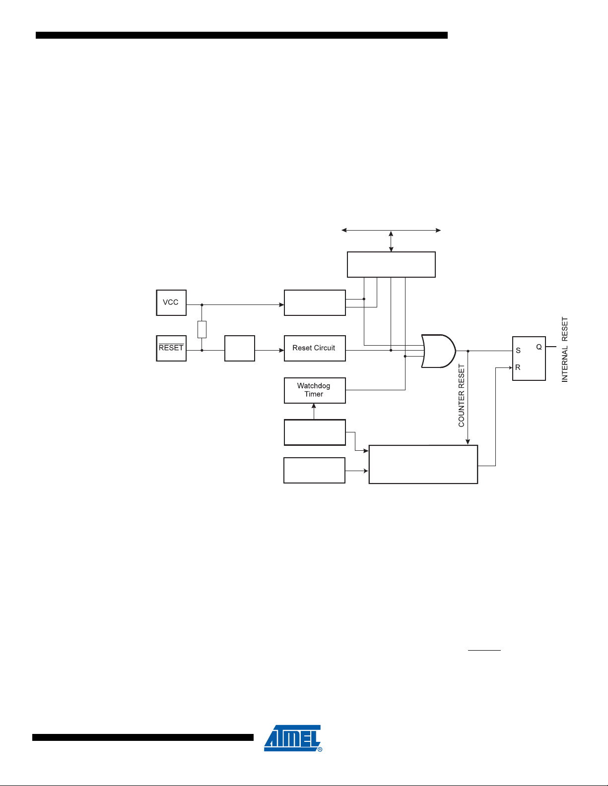
8.1 Resetting the AVR
During reset, all I/O registers are set to their init ial values, and th e pro gram st art s execution from
the Reset Vector. The instruction pl aced at t he Rese t Vecto r must b e a RJMP – Rela tive Ju mp –
instruction to the reset handling routine. If the program never enables an interrupt source, the
interrupt vectors are not used, and regular program code can be placed at these locations. The
circuit diagram in Figure 8-1 shows the reset logic. Electrical parameters of the reset circuitry are
defined in section “System and Reset Characteristics” on page 119.
Figure 8-1. Reset Logic
ATtiny4/5/9/10
8.2 Reset Sources
8127B–AVR–08/09
The I/O ports of the AVR are immediately reset to their initial state when a reset source goes
active. This does not require any clock source to be running.
After all reset sources have gone inactive, a delay counter is invoked, stretching the internal
reset. This allows the power to reach a stable level before normal operation starts. The start up
sequence is described in “Start ing from Reset” on page 20.
The ATtiny4/5/9/10 have three sources of reset:
• Power-on Reset. The MCU is reset when the supply voltage is below the Power-on Reset
threshold (V
• External Reset. The MCU is reset when a low level is present on the RESET
POT
)
pin for longer
than the minimum pulse length
• Watchdog Reset. The MCU is reset when the Watchdog Timer period expires and the
Watchdog is enabled
27
Page 28
ATtiny4/5/9/10
8.2.1 Power-on Reset
V
RESET
TIME-OUT
INTERNAL
RESET
t
TOUT
V
POT
V
RST
CC
RESET
TIME-OUT
INTERNAL
RESET
t
TOUT
V
POT
V
RST
V
CC
A Power-on Reset (POR) pulse is generated by an on-chip detection circuit. The detection level
is defined in section “System and Reset Characteristics” on page 119. The POR is activated
whenever V
is below the detection level. The POR circuit can be used to trigger the Start-up
CC
Reset, as well as to detect a failure in supply voltage.
A Power-on Reset (POR) circuit ensures that the device is reset from Power-on. Reac hing the
Power-on Reset threshold voltage invokes the delay counter, which determines how long the
device is kept in reset after V
V
decreases below the detection level.
CC
rise. The reset signal is activated again, without any delay, when
CC
Figure 8-2. MCU Start-up, RESET
Tied to V
CC
Figure 8-3. MCU Start-up, RESET Extended Externally
Level Monitoring
CC
8.2.2 V
28
ATtiny4/5/9/10 have a V
V
pin against fixed trigger levels. The trigger levels are set with VLM2:0 bits, see “VLMCSR –
CC
Level Monitoring (VLM) circuit that compares the voltage level at the
CC
VCC Level Monitoring Control and Status register” on page 33.
The VLM circuit provides a status flag, VLMF, that indicates if volt age on the V
pin is below the
CC
selected trigger level. The flag can be read from VLMCSR, but it is also possible to have an
interrupt generated when the VLMF status flag is set. This interrupt is enabled by the VLMIE bit
in the VLMCSR register. The flag can be cleared by changing the trigger level or by writing it to
zero. The flag is automatically cleared when the voltage at V
rises back above the selected
CC
trigger level.
8127B–AVR–08/09
Page 29
ATtiny4/5/9/10
CC
The VLM can also be used to improve reset characteristics at falling supply. Without VLM, the
Power-On Reset (POR) does not activate before supply voltage has dropped to a level where
the MCU is not necessarily functional any more. With VLM, it is possible to generate a reset at
supply voltages where the MCU is still functional.
When active, the VLM circuit consumes some power, as illustrated in Figure 17-48 on page 146.
To save power the VLM circuit can be turned off completely, or it can be switched on and off at
regular intervals. However, detection takes some time and it is therefore recommended to leave
the circuitry on long enough for signals to settle. See “VCC Level Monitor” on page 119.
8.2.3 External Reset
When VLM is active and voltage at V
normal and the VLM can be shut down for a short period of time. If voltage at V
is above the selected trigger level operation will be as
CC
drops below
CC
the selected threshold the VLM will either flag an interrupt or generate a reset, depending on the
configuration.
When the VLM has been configured to generate a reset at low supply voltage it will keep the
device in reset as long as V
is below the reset level. See Table 8-4 on page 34 for reset level
CC
details. If supply voltage rises above the reset level the condition is removed and the MCU will
come out of reset, and initiate the power-up start-up sequence.
If supply voltage drops enough to trigger the POR then PORF is set after supply voltage has
been restored.
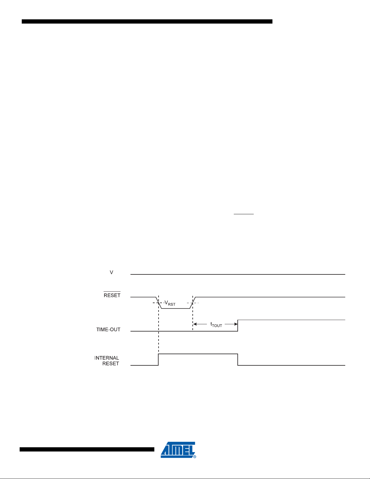
An External Reset is generated by a low level on the RESET
pin if enabled. Reset pulses longer
than the minimum pulse width (see section “System and Reset Characteristics” on page 119)
will generate a reset, even if the clock is not running. Shorter pulses are not guaranteed to generate a reset. When the applied signal reaches the Reset Threshold Voltage – V
positive edge, the delay counter start s the MCU after the time-out period – t
TOUT –
– on its
RST
has expired.
Figure 8-4. External Reset During Operation
8.2.4 Watchdog Reset
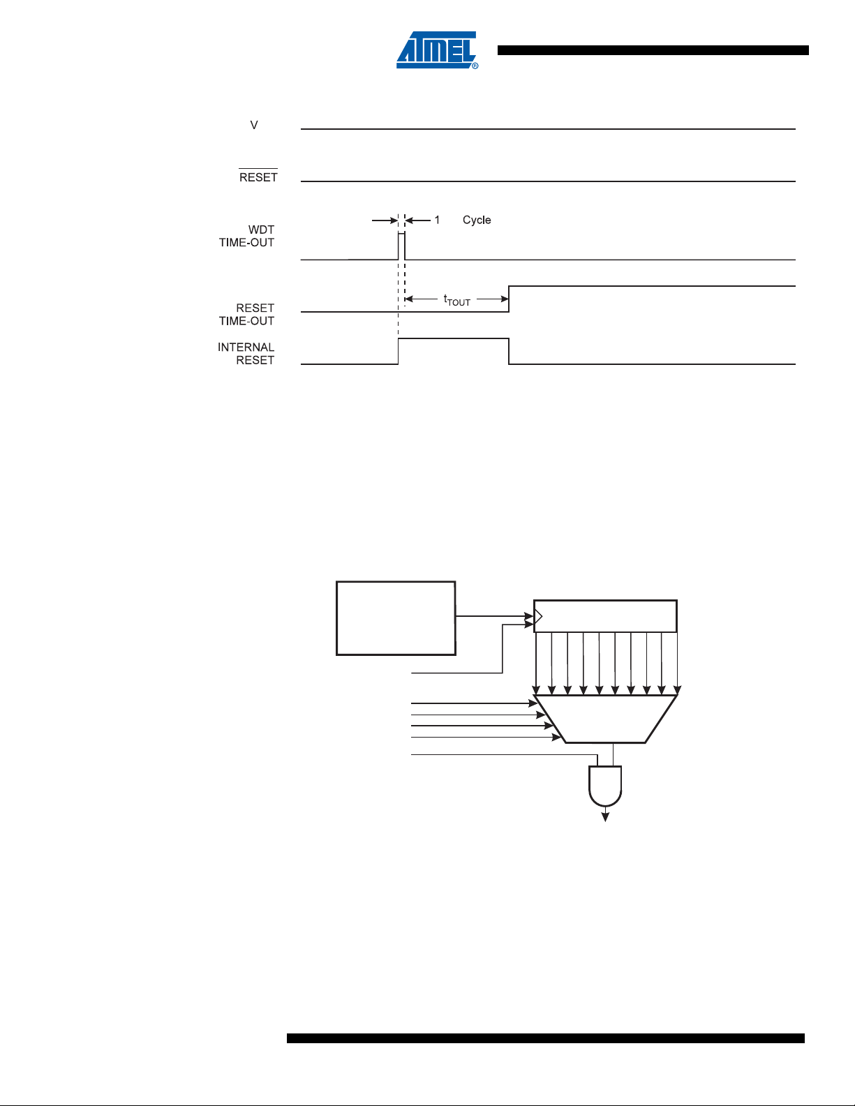
8127B–AVR–08/09
When the Watchdog times out, it will generate a short reset pulse of one CK cycle duration. On
the falling edge of this pulse, the delay timer starts counting the time-out period t
. See page
TOUT
30 for details on operation of the Watchdog Tim er and Table 16-4 on page 119 for details on
reset time-out.
29
Page 30
ATtiny4/5/9/10
Figure 8-5. Watchd og R eset Du rin g Op er a tion
CK
CC
OSC/2K
OSC/4K
OSC/8K
OSC/16K
OSC/32K
OSC/64K
OSC/128K
OSC/256K
OSC/512K
OSC/1024K
MCU RESET
WATCHDOG
PRESCALER
128 kHz
OSCILLATOR
WATCHDOG
RESET
WDP0
WDP1
WDP2
WDP3
WDE
MUX
8.3 Watchdog Timer
The Watchdog Timer is clocked from an on-chip oscillator, which runs at 128 kHz. See Figure 8-
6. By controlling the Watchdog Timer prescaler, the Watchdog Reset interval can be adjusted as
shown in Table 8-2 on page 32. The WDR – Watchdog Reset – instruction resets the Watchdog
Timer. The Watchdog Timer is also reset when it is disabled and when a device reset occurs.
Ten different clock cycle periods can be selected to determine the reset period. If the reset
period expires without another Watchdog Reset, the ATtiny4/5/9/10 resets and executes from
the Reset Vector. For timing details on the Watchdog Reset, refer to Table 8-3 on page 33.
30
Figure 8-6. Watchdog Timer
The Wathdog Timer can also be configured to generate an interrupt instead of a reset. This can
be very helpful when using the Watchdog to wake-up from Power-down.
To prevent unintentional disabling of the Watchd og or unintentional chan ge of time-out period,
two different safety levels are selected by the fuse WDTON as shown in Table 8-1 on page 31.
8127B–AVR–08/09
See “Procedure for Changing the Watchdog Timer Configuration” on page 31 for details.
Page 31

ATtiny4/5/9/10
Table 8-1. WDT Configuration as a Function of the Fuse Settings of WDTON
Safety
WDTON
Unprogrammed 1 Disabled
Programmed 2 Enabled Always enabled
Level
WDT
Initial State
How to
Disable the WDT
Protected change
sequence
8.3.1 Procedure for Changing the Watchdog Timer Configuration
The sequence for changing configuration differs bet ween the two safety levels, as follows:
8.3.1.1 Safety Level 1
In this mode, the Watchdog Timer is initially disabled, but can be enabled by writing the WDE bit
to one without any restriction. A special seque nce is neede d when disab ling an enab led Watchdog Timer. To disable an enabled Watchdog Timer, the following procedure must be followed:
1. Write the signature for change enable of protected I/O registers to register CCP
2. Within four instruction cycles, in the same operation, write WDE and WDP bits
8.3.1.2 Safety Level 2
In this mode, the Watchdog Timer is always enabled, and the WDE bit will always read as one. A
protected change is needed when changing the Watchdog Time-out period. To change the
Watchdog Time-out, the following procedure must be followed:
1. Write the signature for change enable of protected I/O registers to register CCP
2. Within four instruction cycles, write the WDP bit. The value written to WDE is irrelevant
How to
Change Time-out
No limitations
Protected change
sequence
8.3.2 Code Examples
The following code example shows how to turn off the WDT. The example assumes that interrupts are controlled (e.g., by disabling interrupts globally) so that no interrupts will occur during
execution of these functions.
Assembly Code Example
WDT_off:
wdr
; Clear WDRF in RSTFLR
in r16, RSTFLR
andi r16, ~(1<<WDRF)
out RSTFLR, r16
; Write signature for change enable of protected I/O register
ldi r16, 0xD8
out CCP, r16
; Within four instruction cycles, turn off WDT
ldi r16, (0<<WDE)
out WDTCSR, r16
ret
Note: See “Code Examples” on page 5.
8127B–AVR–08/09
31
Page 32

ATtiny4/5/9/10
8.4 Register Description
8.4.1 WDTCSR – Watchdog Timer Control and Status Register
Bit 76543210
0x31 WDIF WDIE WDP3
Read/Write R/W R/W R/W R R/W R/W R/W R/W
Initial Value 0 0 0 0 X 0 0 0
• Bit 7 – WDIF: Watchdog Timer Interrupt Flag
This bit is set when a time-out occurs in the Watchdog Timer and the Watchdog Timer is configured for interrupt. WDIF is cleared by hardware when executing the corresponding interrupt
handling vector. Alternatively, WDIF is cle ar ed by writing a logic one to the flag. When the WDIE
is set, the Watchdog Time-out Interrupt is requested.
• Bit 6 – WDIE: Watchdog Timer Interrupt Enable
When this bit is written to one, the Watchdog interrupt request is enabled. If WDE is cleared in
combination with this setting, the Watchdog Timer is in Interrupt Mode, and the corresponding
interrupt is requested if time-out in the Watchdog Timer occurs.
If WDE is set, the Watchdog Timer is in Interrupt and System Reset Mode. The first time-out in
the Watchdog Timer will set WDIF. Executing the corresponding interrupt vector will clear WDIE
and WDIF automatically by hardware (the Watchdog goes to System Reset Mode). This is useful for keeping the Watchdog Timer security while using the interrupt. To stay in Interrupt and
System Reset Mode, WDIE must be set after each interrupt. This should h owever not be done
within the interrupt service routine itself, as this might compromise the safety-function of the
Watchdog System Reset mode. If the interrupt is not executed before the next time-out, a System Reset will be applied.
– WDE WDP2 WDP1 WDP0 WDTCSR
Table 8-2. Watchdog Timer Configuration
WDTON
Note: 1. WDTON configuration bit set to “0“ means programmed and “1“ means unprogrammed.
(1)
100Stopped None
1 0 1 Interrupt Mode Interrupt
1 1 0 System Reset Mode Reset
111
0 x x System Reset Mode Reset
WDE WDIE Mode Action on Time-out
Interrupt and System
Reset Mode
Interrupt, then go to
System Reset Mode
• Bit 4 – Res: Reserved Bit
This bit is reserved and will always read zero.
• Bit 3 – WDE: Watchdog System Reset Enable
WDE is overridden by WDRF in MCUSR. This means that WDE is always set when WDRF is
set. To clear WDE, WDRF must be cleared first. This feature ensur es multiple reset s during co nditions causing failure, and a safe start-up after the failure.
32
8127B–AVR–08/09
Page 33

ATtiny4/5/9/10
• Bits 5, 2:0 – WDP3..0: Watchdog Timer Prescaler 3, 2, 1 and 0
The WDP3..0 bits determine the Watchdog Timer prescaling when the Watchdog Time r is running. The different prescaling values and their corresponding time-out periods are shown in
Table 8-3 on page 33.
Table 8-3. Watchdog Timer Prescale Select
Number of WDT
WDP3 WDP2 WDP1 WDP0
0000 2K (2048) cycles 16 ms
0001 4K (4096) cycles 32 ms
0010 8K (8192) cycles 64 ms
0011 16K (16384) cycles 0.125 s
0100 32K (32768) cycles 0.25 s
0101 64K (65536) cycles 0.5 s
0110 128K (131072) cycles 1.0 s
0111 256K (262144) cycles 2.0 s
1000 512K (524288) cycles 4.0 s
10011024K (1048576) cycles 8.0 s
1010
1011
1100
1101
1110
1111
Oscillator Cycles
Reserved
Typical Time-out at
VCC = 5.0V
8.4.2 VLMCSR – V
8127B–AVR–08/09
Level Monitoring Control and Status register
CC
Bit 76543210
0x34 VLMF VLMIE
Read/Write R R/W R R R R R/W R/W
Initial Value 0 0 0 0 0 0 0 0
– – – VLM2 VLM1 VLM0 VLMCSR
• Bit 7 – VLMF: VLM Flag
This bit is set by the VLM circuit to indicate that a voltage level conditio n has been triggere d (see
Table 8-4). The bit is cleared when the trigger level selection is set to “Disabled”, or when volt-
age at V
rises above the selected trigger level.
CC
• Bit 6 – VLMIE: VLM Interrupt Enable
When this bit is set the VLM interrupt is enabled. A VLM interrupt is generated every time the
VLMF flag is set.
• Bits 5:3 – Res: Reserved Bits
These bits are reserved. For ensuring compatibility with future devices, these bits must be written to zero, when the register is written.
33
Page 34

ATtiny4/5/9/10
• Bits 2:0 – VLM2:0: Trigger Level of Voltage Level Monitor
These bits set the trigger level for the voltage level monitor, as described in Table 8-4 below.
Table 8-4. Setting the Trigger Level of Voltage Level Monitor.
VLM2:0 Label Description
000 VLM0 Voltage Level Monitor disabled
001 VLM1L
010 VLM1H
011 VLM2
100 VLM3
101
111
For VLM voltage levels, see TBD, TBD and TBD.
8.4.3 RSTFLR – Reset Flag Register
The Reset Flag Register provides information on which reset source caused an MCU Reset.
Bit 76543210
0x3B
Read/Write R R R R R/W R R/W R/W
Initial Value 0 0 0 0 X 0 X X
• Bits 7:4, 2– Res: Reserved Bits
These bits are reserved bits in ATtiny4/5/9/10 and will always read as zero.
• Bit 3 – WDRF: Watchdog Reset Flag
This bit is set if a Watchdog Reset occurs. The bit is reset by a Power-on Reset, or by writing a
logic zero to the flag.
Triggering generates a regular Power-On Reset (POR).
The VLM flag is not set
Triggering sets the VLM Flag (VLMF) and generates a VLM
interrupt, if enabled
Not allowed110
– – – – WDRF – EXTRF PORF RSTFLR
34
• Bit 1 – EXTRF: External Reset Flag
This bit is set if an External Reset occurs. The bit is reset by a Power-on Reset, or by writing a
logic zero to the flag.
• Bit 0 – PORF: Power-on Reset Flag
This bit is set if a Power-on Reset occurs. The bit is reset only by writing a logic zero to the flag.
To make use of the Reset Flags to identify a r eset condition, t he user should r ead and t hen reset
the MCUSR as early as possible in the prog ram. If the register is cle ared before anot her reset
occurs, the source of the reset can be found by examining the Reset Flags.
8127B–AVR–08/09
Page 35

9. Interrupts
This section describes the specifics of the interrupt handling in ATtiny4/5/9/10. For a general
explanation of the AVR interrupt handling, see “Reset and Interrupt Handling” on page 10.
9.1 Interrupt Vectors
Interrupt vectors of ATtiny4/5/9/10 are described in Table 9-1 below.
Table 9-1. Reset and Interrupt Vectors
ATtiny4/5/9/10
Vector No. Program Address Label Interrupt Source
1 0x0000 RESET
2 0x0001 INT0 External Interrupt Request 0
3 0x0002 PCINT0 Pin Change Interrupt Request 0
4 0x0003 TIM0_CAPT Timer/Counter0 Input Capture
5 0x0004 TIM0_OVF Timer/Counter0 Overflow
6 0x0005 TIM0_COMPA Timer/Counter0 Compare Match A
7 0x0006 TIM0_COMPB Timer/Counter0 Compare Match B
External Pin, Power-on Reset,
VLM Reset, Watchdog Reset
8 0x0007 ANA_COMP Analog Comparator
9 0x0008 WDT Watchdog Time-out
10 0x0009 VLM V
11 0x000A ADC ADC Conversion Complete
Note: 1. The ADC is available in ATtiny5/10, only.
Voltage Level Monitor
CC
(1)
In case the program never enables an interrupt source, the Interrupt Vectors will not be used
and, consequently, regular program code can be pl aced at these locations.
The most typical and general setup for interrupt vector addresses in ATtiny4/5/9/10 is shown in
the program example below.
Address Labels Code Comments
0x0000 rjmp RESET ; Reset Handler
0x0001 rjmp INT0 ; IRQ0 Handler
0x0002 rjmp PCINT0 ; PCINT0 Handler
0x0003 rjmp TIM0_CAPT ; Timer0 Capture Handler
0x0004 rjmp TIM0_OVF ; Timer0 Overflow Handler
0x0005 rjmp TIM0_COMPA ; Timer0 Compare A Handler
0x0006 rjmp TIM0_COMPB ; Timer0 Compare B Handler
0x0007 rjmp ANA_COMP ; Analog Comparator Handler
0x0008 rjmp WDT ; Watchdog Interrupt Handler
0x0009 rjmp VLM ; Voltage Level Monitor Handler
0x000A rjmp ADC ; ADC Conversion Handler
8127B–AVR–08/09
<continues>
35
Page 36

ATtiny4/5/9/10
9.2 External Interrupts
External Interrupts are triggered by the INT0 pin or any of the PCINT3..0 pins. Observ e that, if
enabled, the interrupts will trigger even if the INT0 or PCINT3..0 pins are configured as outputs.
This feature provides a way of generating a software interrupt. Pin change 0 interrupts PCI0 will
trigger if any enabled PCINT3..0 pin toggles. The PCMSK Register controls which pins contribute to the pin change interrupts. Pin change interrupts on PCINT3..0 are detected
asynchronously, which means that these interrupts can be used for waking the part also from
sleep modes other than Idle mode.
The INT0 interrupt can be triggered by a falling or rising edge or a low level. This is set up as
shown in “EICRA – External Interrupt Con trol Regist er A” on page 37. When the INT0 interrupt is
enabled and configured as level triggered, the interrupt will trigger as long as the pin is held low.
Note that recognition of falling or rising edge interrupts on INT0 requires the presence of an I/O
clock, as described in “Clock System” on page 17.
<continued>
0x000B RESET: ldi r16, high(RAMEND); Main program start
0x000C out SPH,r16 ; Set Stack Pointer
0x000D ldi r16, low(RAMEND) ; to top of RAM
0x000E out SPL,r16
0x000F sei ; Enable interrupts
0x0010 <instr>
... ...
9.2.1 Low Level Interrupt
A low level interrupt on INT0 is detected asynchronously. This means that the interrupt source
can be used for waking the part also from sleep modes other than Idle (the I/O clock is halted in
all sleep modes except Idle).
Note that if a level triggered interrupt is used for wake-up from Power -down, the required level
must be held long enough for the MCU to complete the wake-up to trigger the level interrupt. If
the level disappears before the end of the Start-up Time, the MCU will still wake up, but no interrupt will be generated. The start-up time is defined as described in “Clock System” on page 17.
If the low level on the interrupt pin is removed before the device has woken up then program
execution will not be diverted to the interrupt service routine but continue from the instruction following the SLEEP command.
9.2.2 Pin Change Interrupt Timing
A timing example of a pin change interrupt is shown in Figure 9-1.
36
8127B–AVR–08/09
Page 37

Figure 9-1. Timing of pin change interrupts
clk
PCINT(0)
pin_lat
pin_sync
pcint_in_(0)
pcint_syn
pcint_setflag
PCIF
PCINT(0)
pin_sync
pcint_syn
pin_lat
D Q
LE
pcint_setflag
PCIF
clk
clk
PCINT(0) in PCMSK(x)
pcint_in_(0)
0
x
ATtiny4/5/9/10
9.3 Register Description
9.3.1 EICRA – External Interrupt Control Register A
The External Interrupt Control Register A contains control bits for interrupt sense control.
Bit 76543210
0x15
Read/Write RRRRRRR/WR/W
Initial Value 0 0 0 0 0 0 0 0
– – – – – – ISC01 ISC00 EICRA
• Bits 7:2 – Res: Reserved Bits
These bits are reserved and will always read zero.
• Bits 1:0 – ISC01, ISC00: Interrupt Sense Control 0 Bit 1 and Bit 0
The External Interrupt 0 is activated by the external pin INT0 if the SREG I-flag and the corresponding interrupt mask are set. The level and edges on the external INT0 pin that activate the
interrupt are defined in Table 9-2. The value on the INT0 pin is sampled before detecting edges.
If edge or toggle interrupt is selected, pulses that last longer than one clock period will generate
an interrupt. Shorter pulses are not guaranteed to generate an interrupt. If low level interrupt is
37
8127B–AVR–08/09
Page 38

ATtiny4/5/9/10
selected, the low level must be held until the completion of the currently executing instruction to
generate an interrupt.
Table 9-2. Interrupt 0 Sense Control
ISC01 ISC00 Description
0 0 The low level of INT0 generates an interrupt request.
0 1 Any logical change on INT0 generates an interrupt request.
1 0 The falling edge of INT0 generates an interrupt request.
1 1 The rising edge of INT0 generates an interrupt request.
9.3.2 EIMSK – External Interrupt Mask Re gister
Bit 76543210
0x13
Read/Write RRRRRRRR/W
Initial Value 0 0 0 0 0 0 0 0
– – – – – – –INTOEIMSK
• Bits 7:1 – Res: Reserved Bits
These bits are reserved and will always read zero.
• Bit 0 – INT0: External Interrupt Request 0 Enable
When the INT0 bit is set (one) and the I-bit in the Status Register (SREG) is set (one), the external pin interrupt is enabled. The Interrupt Sense Control bits (ISC01 and ISC00) in the External
Interrupt Control Register A (EICRA) define whether the external interrupt is activated on rising
and/or falling edge of the INT0 pin or level sensed. Activity on the pin will cause an interrupt
request even if INT0 is configured as an ou tput. The correspond ing inter rupt of External I nterrupt
Request 0 is executed from the INT0 Interrupt Vector.
9.3.3 EIFR – External Interrupt Flag Register
Bit 76543210
0x14
Read/Write RRRRRRRR/W
Initial Value 0 0 0 0 0 0 0 0
– – – – – – – INTF0 EIFR
• Bits 7:1 – Res: Reserved Bits
These bits are reserved and will always read zero.
• Bit 0 – INTF0: External Interrupt Flag 0
When an edge or logic change on the INT0 pin triggers an interrup t requ est, INTF0 be comes set
(one). If the I-bit in SREG and the INT0 bit in EIMSK are set (one), the MCU will jump to the corresponding Interrupt Vector.
The flag is cleared when the interrupt routine is executed. Alternatively, the flag can be cleared
by writing a logical one to it.
This flag is constantly zero when INT0 is configured as a level interrupt.
38
8127B–AVR–08/09
Page 39

9.3.4 PCICR – Pin Change Interrupt Control Register
Bit 76543210
0x12
Read/Write RRRRRRRR/W
Initial Value 0 0 0 0 0 0 0 0
– – – – – – –PCIE0PCICR
• Bits 7:1 – Res: Reserved Bits
These bits are reserved and will always read zero.
• Bit 0 – PCIE0: Pin Change Interrupt Enable 0
When the PCIE0 bit is set (one) and the I-bit in the Status Register (SREG) is set (one), pin
change interrupt 0 is enabled. Any change on any enabled PCINT3..0 pin will cause an interrupt.
The corresponding interrupt of Pin Change Interrupt Request is executed from the PCI0 Interrupt Vector. PCINT3..0 pins are enabled individua lly by the PCMSK Register.
9.3.5 PCIFR – Pin Change Interrupt Flag Register
Bit 76543210
0x11
Read/Write RRRRRRRR/W
Initial Value 0 0 0 0 0 0 0 0
– – – – – – – PCIF0 PCIFR
ATtiny4/5/9/10
• Bits 7:1 – Res: Reserved Bits
These bits are reserved and will always read zero.
• Bit 0 – PCIF0: Pin Change Interrupt Flag 0
When a logic change on any PCINT3..0 pin triggers an interrupt request, PCIF0 becomes set
(one). If the I-bit in SREG and the PCIE0 bit in PCICR are set (one), the MCU will jump to the
corresponding Interrupt Vector. The flag is cleared when the interrupt routine is executed. Alternatively, the flag can be cleared by writing a logical one to it.
9.3.6 PCMSK – Pin Change Mask Register
Bit 76543210
0x10
Read/Write R R R R R/W R/W R/W R/W
Initial Value 0 0 0 0 0 0 0 0
– – – – PCINT3 PCINT2 PCINT1 PCINT0 PCMSK
• Bits 7:4 – Res: Reserved Bits
These bits are reserved and will always read zero.
• Bits 3:0 – PCINT3..0: Pin Change Enable Mask 3..0
Each PCINT3..0 bit selects whether pin change interrupt is enabled on the corresponding I/O
pin. If PCINT3..0 is set and the PCIE0 bit in PCICR is set, pin change interrupt is enabled on the
corresponding I/O pin. If PCINT3..0 is cle ar ed, p in ch ang e inter rup t on t he correspo nd ing I/O pin
is disabled.
8127B–AVR–08/09
39
Page 40

ATtiny4/5/9/10
10. I/O Ports
C
pin
Logic
R
pu
See Figure
"General Digital I/O" for
Details
Pxn
10.1 Overview
All AVR ports have true Read-Modify-Write functionality when used as general digital I/O ports.
This means that the direction of one port pin can be changed without unintentionally changing
the direction of any other pin with the SBI and CBI instructions. The same applies when changing drive value (if configured as output) or enabling/disabling of pull-up resistors. Each output
buffer has symmetrical drive characteristics with both high sink and source capability. The pin
driver is strong enough to drive LED displays directly. All port pins have ind ividually selectable
pull-up resistors with a supply-voltage invariant resistance. All I/O pins ha ve prote ctio n diod es to
both V
page 116 for a complete list of parameters.
Figure 10-1. I/O Pin Equivalent Schematic
and Ground as indicated in Figure 10-1 on pag e 40 . See “Electrical Characteristics” on
CC
40
All registers and bit references in this section are written in general form. A lower case “x” r epresents the numbering letter for the port, and a lower case “n” rep resents the bit number. However,
when using the register or bit defines in a program , the precise form must be used. For examp le,
PORTB3 for bit no. 3 in Port B, here documented ge ner ally as PO RTxn . The physical I /O Registers and bit locations are listed in “Register Description” on page 50.
Four I/O memory address locations are allocated fo r each por t, on e each for the Data Regist er –
PORTx, Data Direction Register – DDRx, Pull-up Enable Register – PUEx, and the Port Input
Pins – PINx. The Port Input Pins I/O location is read only, while the Data Register, the Data
Direction Register, and the Pull-up Enable Register are read/write. However, writing a logic one
to a bit in the PINx Register, will result in a toggle in the corresponding bit in the Data Register.
Using the I/O port as General Digital I/O is described in “Ports as General Digital I/O” on page
41. Most port pins are multiplexed with alternate func tions for the peripheral featur es on the
device. How each alternate function interferes with the port pin is described in “Alternate Port
Functions” on page 45. Refer to the individual module sections for a full description of the alter-
nate functions.
Note that enabling the alternate function of some of the port pins does not affect the use of the
other pins in the port as general digital I/O.
8127B–AVR–08/09
Page 41

10.2 Ports as General Digital I/O
clk
RPx
RRx
RDx
WDx
WEx
SYNCHRONIZER
WDx: WRITE DDRx
WRx: WRITE PORTx
RRx: READ PORTx REGISTER
RPx: READ PORTx PIN
clk
I/O
: I/O CLOCK
RDx: READ DDRx
WEx: WRITE PUEx
REx: READ PUEx
DLQ
Q
REx
RESET
RESET
Q
QD
Q
QD
CLR
PORTxn
Q
QD
CLR
DDxn
PINxn
DATA BUS
SLEEP
SLEEP: SLEEP CONTROL
Pxn
I/O
WPx
RESET
Q
QD
CLR
PUExn
0
1
WRx
WPx: WRITE PINx REGISTER
The ports are bi-directional I/O ports with optional internal pull-ups. Figure 10-2 shows a functional description of one I/O-port pin, here generically called Pxn.
ATtiny4/5/9/10
Figure 10-2. General Digital I/O
(1)
Note: 1. WEx, WRx, WPx, WDx, REx, RRx, RPx, and RDx are common to all pins within the same
10.2.1 Configuring the Pin
Each port pin consists of four register bits: DDxn, PORTxn, PUExn, and PINxn. As shown in
“Register Description” on page 50 , the DDxn bits are accesse d at the DDRx I/O addres s, the
PORTxn bits at the PORTx I/O address, the PUExn bits at the PUEx I /O addr ess, and the PINxn
bits at the PINx I/O address.
8127B–AVR–08/09
port. clk
, and SLEEP are common to all ports.
I/O
41
Page 42

ATtiny4/5/9/10
The DDxn bit in the DDRx Register selects the direction of this pin. If DDxn is written logic one,
Pxn is configured as an output pin. If DDxn is written logic zero, Pxn is configured as an input
pin.
If PORTxn is written logic one when the pin is configured as an output pin, the port pin is driven
high (one). If PORTxn is written logic zero when the pin is configured as an output pin, the port
pin is driven low (zero).
The pull-up resistor is activated, if the PUExn is written logic one. To switch the pull-up resistor
off, PUExn has to be written logic zero.
Table 10-1 summarizes the control signals for the pin value.
Table 10-1. Port Pin Configurations
DDxn PORTxn PUExn I/O Pull-up Comment
0X
0X
10
10
11
11
Port pins are tri-stated when a reset condition becomes active, even when no clocks are
running.
10.2.2 To ggling the Pin
Writing a logic one to PINxn toggles the value of PORTxn, independent on the value of DDRxn.
Note that the SBI instruction can be used to toggle one single bit in a port.
10.2.3 Break-Before-Make Switching
In Break-Before-Make mode, switching the DDRxn bit from input to output introduces an immediate tri-state period lasting on e system clock cycle, as indicated in Figure 10-3. For example, if
the system clock is 4 MHz and the DDRxn is written to make an output, an immediate tri-state
period of 250 ns is introduced before the value of PORTxn is seen on th e port pin.
0
1
0
1
0
1
Input No Tri-state (hi-Z)
Input Yes Sources current if pulled low externally
Output No Output low (sink)
NOT RECOMMENDED.
Output Yes
Output No Output high (source)
Output Yes Output high (source) and internal pull-up active
Output low (sink) and internal pull-up active.
Sources current through the internal pull-up
resistor and consumes power constantly
42
To avoid glitches it is recommended that the maximum DDRxn toggle frequency is two system
clock cycles. The Break-Before-Make mode applies to the entire port and it is activated by the
BBMx bit. For more details, see “PORTCR – Port Control Register” on page 50.
When switching the DDRxn bit from output to input no immediate tri-state period is introduced.
8127B–AVR–08/09
Page 43

Figure 10-3. Switching Between Input and Output in Break-Before-Make-Mode
out DDRx, r16 nop
0x02 0x01
SYSTEM CLK
INSTRUCTIONS
DDRx
intermediate tri-state cycle
out DDRx, r17
0x55
PORTx
0x01
intermediate tri-state cycle
Px0
Px1
tri-state
tri-statetri-state
0x01
r17
0x02
r16
10.2.4 Reading the Pin Value
Independent of the setting of Data Direction b it DDxn, the port pin can be read through the
PINxn Register bit. As shown in Figure 10-2 on page 41, the PINxn Register bit a nd th e pr eceding latch constitute a synchronizer. This is needed to avoid metastability if the physical pin
changes value near the edge of the internal clock, but it also introduces a delay. Figure 10-4
shows a timing diagram of the synchronization when reading an externally applied pin value.
The maximum and minimum propagation delays are denoted t
ATtiny4/5/9/10
pd,max
and t
respectively.
pd,min
Figure 10-4. Synchronization when Reading an Externally Applied Pin value
Consider the clock period starting shortly after the first falling edge of the system clock. The latch
is closed when the clock is low, and goes transparent when the clock is high, as indicated by the
shaded region of the “SYNC LATCH” signal. The signal value is latched when the system clock
goes low. It is clocked into the PINxn Register at the succeeding positive clock edge. As indicated by the two arrows tpd,max and tpd,min, a single signal transition on the pin will be delayed
between ½ and 1½ system clock period depending upon the time of assertion.
SYSTEM CLK
INSTRUCTIONS
SYNC LATCH
PINxn
r17
XXX in r17, PINx
XXX
0x00 0xFF
t
pd, max
t
pd, min
8127B–AVR–08/09
43
Page 44
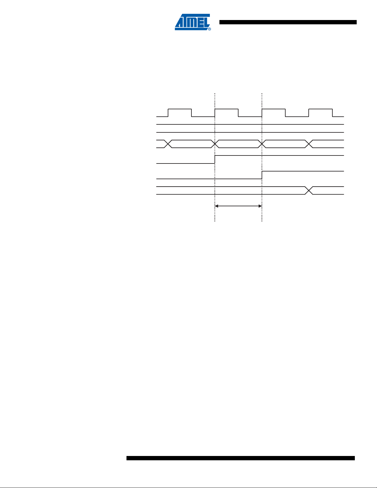
ATtiny4/5/9/10
When reading back a software assigned pin value, a nop instruction must be inserted as indicated in Figure 10-5 on page 44. The out instruction sets the “SYNC LATCH” signal at the
positive edge of the clock. In this case, the delay tpd through the synchronizer is one system
clock period.
Figure 10-5. Synchronization when Reading a Software Assigned Pin Value
SYSTEM CLK
r16
INSTRUCTIONS
SYNC LATCH
PINxn
r17
10.2.5 Digital Input Enable and Sleep Modes
As shown in Figure 10-2 on page 41, the digital input signal can be clamped to ground at the
input of the schmitt-trigger. The signal denoted SLEEP in the figure, is set by the MCU Sleep
Controller in Power-down and Standby modes to avoid high power consumption if some input
signals are left floating, or have an analog signal level close to V
SLEEP is overridden for port pins enabled as external interrupt pins. If the external interrupt
request is not enabled, SLEEP is active also for these pins. SLEEP is also overridden by various
other alternate functions as described in “Alternate Port Functions” on page 45.
0xFF
out PORTx, r16 nop in r17, PINx
0x00 0xFF
t
pd
/2.
CC
10.2.6 Unconnected Pins
44
If a logic high level (“one”) is present on an asynchronous external interrupt pin configured as
“Interrupt on Rising Edge, Falling Edge, or Any Logic Change on Pin” while the extern al interrupt
is not enabled, the corresponding External Interrupt Flag will be set when resuming from the
above mentioned Sleep mode, as the clamping in these sleep mode produces the requested
logic change.
If some pins are unused, it is recommended to ensure t hat these pins have a defi ned level. Even
though most of the digital inputs are disabled in th e deep sleep modes as de scribed above, floating inputs should be avoided to reduce current consumption in all other modes where the digital
inputs are enabled (Reset, Active mode and Idle mode).
The simplest method to ensure a defined level of an unused pin, is to enable the internal pull-up.
In this case, the pull-up will be disabled during reset. If low power consumption during reset is
important, it is recommended to use an external pull-up or pulldown. Connecting unused pins
directly to V
or GND is not recommended, since this may caus e excessiv e currents if t he pin is
CC
accidentally configured as an output.
8127B–AVR–08/09
Page 45

10.2.7 Program Example
The following code example shows how to set port B pin 0 high, pin 1 low, and define the port
pins from 2 to 3 as input with a pull-up assigned to port pin 2. The resulting pin values are read
back again, but as previously discussed, a nop instruction is included to be able to read back the
value recently assigned to some of the pins.
Assembly Code Example
ATtiny4/5/9/10
...
; Define pull-ups and set outputs high
; Define directions for port pins
ldi r16,(1<<PUEB2)
ldi r17,(1<<PB0)
ldi r18,(1<<DDB1)|(1<<DDB0)
out PUEB,r16
out PORTB,r17
out DDRB,r18
; Insert nop for synchronization
nop
; Read port pins
in r16,PINB
...
Note: See “Code Examples” on page 5.
10.3 Alternate Port Functions
Most port pins have alternate functions in addition to being general digital I/Os. In Figure 10-6
below is shown how the port pin control signals from the simplified Figure 10-2 on page 41 can
be overridden by alternate functions.
8127B–AVR–08/09
45
Page 46

ATtiny4/5/9/10
Figure 10-6. Alternate Port Functions
(1)
PUOExn
1
0
PUOVxn
DDOExn
1
0
DDOVxn
PVOExn
PVOVxn
Pxn
1
0
DIEOExn
1
0
DIEOVxn
SLEEP
QD
PORTxn
Q
CLR
RESET
SYNCHRONIZER
SET
DLQ
CLR
Q
PINxn
QD
Q
CLR
QD
PUExn
Q
CLR
RESET
QD
DDxn
Q
CLR
RESET
REx
WEx
WDx
RDx
1
0
PTOExn
DATA BUS
RRx
WPx
WRx
RPx
clk
I/O
DIxn
AIOxn
PUOExn: Pxn PULL-UP OVERRIDE ENABLE
PUOVxn: Pxn PULL-UP OVERRIDE VALUE
DDOExn: Pxn DATA DIREC TION OVERRIDE ENABLE
DDOVxn: Pxn DATA DIRECTION OVERRIDE VALUE
PVOExn: Pxn PORT VALUE OVERRIDE ENABLE
PVOVxn: Pxn PORT VALUE OVERRIDE VALUE
DIEOExn: Pxn DIGITAL INPUT-ENABLE OVERRIDE ENABLE
DIEOVxn: Pxn DIGITAL INPUT-ENABLE OVERRIDE VALUE
SLEEP: SLEEP CONTROL
PTOExn: Pxn, PORT TOGGLE OVERRIDE ENABLE
WEx: WRITE PUEx
REx: READ PUEx
WDx: WRITE DDRx
RDx: READ DDRx
RRx: READ PORTx REGISTER
WRx: WRITE PORTx
RPx: READ PORTx PIN
WPx: WRITE PINx
clk
: I/O CLOCK
I/O
DIxn: DIGITAL INPUT PIN n ON PORTx
AIOxn: ANALOG INPUT/OUTPUT PIN n ON PORTx
Note: 1. WEx, WRx, WPx, WDx, REx, RRx, RPx, and RDx are common to all pins within the same
port. clk
, and SLEEP are common to all ports. All other signals are unique for each pin.
I/O
The illustration in the figure above serves as a generic description ap plicable to all port pins in
the AVR microcontroller family. Some overriding signals may not be present in all port pins.
46
8127B–AVR–08/09
Page 47

ATtiny4/5/9/10
Table 10-2 on page 47 summarizes the functio n of the overriding signals. The pin and port
indexes from Figure 10-6 on page 46 are not shown in the succ eeding tables. The overriding
signals are generated internally in the modules having the alternate function.
Table 10-2. Generic Description of Overriding Signals for Alternate Functions
Signal Name Full Name Description
If this signal is set, the pull-up enable is controlled by the PUOV
signal. If this signal is cleared, the pull-up is enabled when
PUExn = 0b1.
If PUOE is set, the pull-up is enabled/disabled when PUOV is
set/cleared, regardless of the setting of the PUExn Register bit.
If this signal is set, the Output Driver Enable is controlled by the
DDOV signal. If this signal is cleared, the Output driver is
enabled by the DDxn Register bit.
If DDOE is set, the Output Driver is enabled/disabled when
DDOV is set/cleared, regardless of the setting of the DDxn
Register bit.
If this signal is set and the Output Driver is enabled, the port
value is controlled by the PVOV signal. If PVOE is cleared, and
the Output Driver is enabled, the port Value is controlled by the
PORTxn Register bit.
If PVOE is set, the port value is set to PVOV, regardless of the
setting of the PORTxn Register bit.
If PTOE is set, the PORTxn Register bit is inverted.
PUOE
PUOV
DDOE
DDOV
PVOE
PVOV
PTOE
Pull-up Override
Enable
Pull-up Override
Value
Data Direction
Override Enable
Data Direction
Override Value
Port Value
Override Enable
Port Value
Override Value
Port Toggle
Override Enable
Digital Input
DIEOE
DIEOV
DI Digital Input
AIO
Enable Override
Enable
Digital Input
Enable Override
Value
Analog
Input/Output
If this bit is set, the Digital Input Enable is controlled by the
DIEOV signal. If this signal is cleared, the Digital Input Enable
is determined by MCU state (Normal mode, sleep mode).
If DIEOE is set, the Digital Input is enabled/disabled when
DIEOV is set/cleared, regardless of the MCU state (Normal
mode, sleep mode).
This is the Digital Input to alternate functions. In the figure, the
signal is connected to the output of the schmitt-trigger but
before the synchronizer. Unless the Digital Input is used as a
clock source, the module with the alternate function will use its
own synchronizer.
This is the Analog Input/Output to/from alternate functions. The
signal is connected directly to the pad, and can be used bidirectionally.
The following subsections shortly describe the alternate functions for each port, and relate the
overriding signals to the alternate function. Refer to the alternate function description for further
details.
8127B–AVR–08/09
47
Page 48

ATtiny4/5/9/10
10.3.1 Alternate Functions of Port B
The Port B pins with alternate function are shown in Table 10-3 on page 48.
Table 10-3. Port B Pins Alternate Functions
Port Pin Alternate Function
PB0
PB1
PB2
ADC0: ADC Input Channel 0
AIN0: Analog Comparator, Positive Input
OC0A: Timer/Counte r0 Compare Match A Output
PCINT0:Pin Change Interrupt 0, Source 0
TPIDATA:Serial Programming Data
ADC1: ADC Input Channel 1
AIN1: Analog Comparator, Negative Input
CLKI: External Clock
ICP0: Timer/Counter0 Input Capture Input
OC0B: Timer/Counte r0 Compare Match B Output
PCINT1:Pin Change Interrupt 0, Source 1
TPICLK: Serial Programming Clock
ADC2: ADC Input Channel 2
CLKO: System Clock Output
INT0: External Interrupt 0 Source
PCINT2:Pin Change Interrupt 0, Source 2
T0: Timer/Counter0 Clock Source
ADC3: ADC Input Channel 3
PB3
PCINT3:Pin Change Interrupt 0, Source 3
RESET
: Reset Pin
• Port B, Bit 0 – ADC0/AIN0/OC0A/PCINT0/TPIDATA
• ADC0: Analog to Digital Converter, Channel 0
(ATtiny5/10, only)
• AIN0: Analog Comparat or Positive Input. Configure the port pin as input with the internal pullup switched off to avoid the digital port function from interfering with the function of the
Analog Comparator.
• OC0A, Output Compare Match output: The PB0 pin can serve as an external output for the
Timer/Counter0 Compare Match A. The pin has to be configured as an output (DDB0 set
(one)) to serve this function. This is also the output pin for the PWM mode timer function.
• PCINT0: Pin Change Interrupt source 0. The PB0 pin can serve as an external interrupt
source for pin change interrupt 0.
• TPIDATA: Serial Programming Data.
• Port B, Bit 1 – ADC1/AIN1/CLKI/ICP0/OC0B/PCINT1/TPICLK
• ADC1: Analog to Digital Converter, Channel 1
(ATtiny5/10, only)
• AIN1: Analog Comparator Negative Input. Configu re the port pin as input with the internal
pull-up switched off to avoid the digital port function from interfering with the function of the
Analog Comparator.
• CLKI: External Clock.
• ICP0: Input Capture Pin. The PB1 pin can act as an Input Capture pin for Timer/Counter0.
48
8127B–AVR–08/09
Page 49

ATtiny4/5/9/10
• OC0B: Output Compare Match output: The PB1 pin can serve as an external output for the
Timer/Counter0 Compare Match B. The PB1 pin has to be configured as an output (DDB1
set (one)) to serve this function. The OC0B pin is also the output pin f or the PWM mode timer
function.
• PCINT1: Pin Change Interrupt source 1. The PB1 pin can serve as an external interrupt
source for pin change interrupt 0.
• TPICLK: Serial Programming Clock.
• Port B, Bit 2 – ADC2/CLKO/INT0/PCINT2/T0
• ADC2: Analog to Digital Converter, Channel 2
• CLKO: System Clock Output. The system clock can be output on pin PB2. The system clock
will be output if CKOUT bit is programmed, regardless of the POR TB2 and DDB2 settings.
• INT0: External Interrupt Request 0
• PCINT2: Pin Change Interrupt source 2. The PB2 pin can serve as an external interrupt
source for pin change interrupt 0.
• T0: Timer/Counter0 counter source.
• Port B, Bit 3 – ADC3/PCINT3/RESET
• ADC3: Analog to Digital Converter, Channel 3 (ATtiny5/10, only)
• PCINT3: Pin Change Interrupt source 3. The PB3 pin can serve as an external interrupt
source for pin change interrupt 0.
• RESET
:
(ATtiny5/10, only)
Table 10-4 and Table 10-5 on page 50 relate the alternate functions of Port B to the overriding
signals shown in Figure 10-6 on page 46.
Table 10-4. Overriding Signals for Alternate Functions in PB3..PB2
Signal
Name PB3/ADC3/RESET
PUOE RSTDISBL
PUOV 1 0
DDOE RSTDISBL
DDOV 0 1
PVOE 0 CKOUT
PVOV 0 (system clock)
PTOE 0 0
DIEOE
DIEOV RSTDISBL • PCINT3 • PCIE0 (PCINT2 • PCIE0) + INT0
DI PCINT3 Input INT0/T0/PCINT2 Input
AIO ADC3 Input ADC2 Input
Notes: 1. RSTDISBL is 1 when the configuration bit is “0” (Programmed).
2. CKOUT is 1 when the configuration bit is “0” (Programmed).
RSTDISBL
ADC3D
(1)
(1)
(1)
/PCINT3 PB2/ADC2/INT0/T0/CLKO/PCINT2
(2)
(2)
(2)
+ (PCINT3 • PCIE0) +
CKOUT
CKOUT
(PCINT2 • PCIE0) + ADC2D + INT0
8127B–AVR–08/09
49
Page 50

ATtiny4/5/9/10
Table 10-5. Overriding Signals for Alternate Functions in PB1..PB0
Signal
Name PB1/ADC1/AIN1/OC0B/CLKI/ICP0/PCINT1 PB0/ADC0/AIN0/OC0A/PCINT0
PUOE EXT_CLOCK
PUOV 0 0
DDOE EXT_CLOCK
DDOV 0 0
PVOE EXT_CLOCK
PVOV EXT_CLOCK
PTOE 0 0
DIEOE
DIEOV
EXT_CLOCK
ADC1D
(EXT_CLOCK
(EXT_CLOCK
DI CLOCK/ICP0/PCINT1 Input PCINT0 Input
AIO ADC1/Analog Comparator Negative Input ADC0/Analog Comparator Positive Input
Notes: 1. EXT_CLOCK is 1 when external clock is selected as main clock.
(1)
(1)
(1)
+ OC0B Enable OC0A Enable
(1)
• OC0B OC0A
(1)
+ (PCINT1 • PCIE0) +
(1)
• PWR_DOWN) +
(1)
• PCINT1 • PCIE0)
0
0
(PCINT0 • PCIE0) + ADC0D
PCINT0 • PCIE0
10.4 Register Description
10.4.1 PORTCR – Port Control Register
Bit 7 6 5 4 3 2 1 0
0x03
Read/Write R R R R R R R/W R
Initial Value 0 0 0 0 0 0 0 0
• Bits 7:2, 0 – Reserved
These bits are reserved and will always read zero.
• Bit 1 – BBMB: Break-Before-Make Mode Enable
When this bit is set the Break-Before-Make mode is activated for the entire Port B. The intermediate tri-state cycle is then inserted when writing DDRxn to make an output. For further
information, see “Break-Before-Make Switching” on page 42.
10.4.2 PUEB – Port B Pull-up Enable Control Register
Bit 76543210
0x03
Read/Write R R R R R/W R/W R/W R/W
Initial Value 0 0 0 0 0 0 0 0
– – – – – – BBMB –PORTCR
– – – – PUEB3 PUEB2 PUEB1 PUEB0 PUEB
50
8127B–AVR–08/09
Page 51

10.4.3 PORTB – Port B Data Register
Bit 76543210
0x02
Read/Write R R R R R/W R/W R/W R/W
Initial Value 0 0 0 0 0 0 0 0
– – – – PORTB3 PORTB2 PORTB1 PORTB0 PORTB
10.4.4 DDRB – Port B Data Direction Register
Bit 76543210
0x01
Read/Write R R R R R/W R/W R/W R/W
Initial Value 0 0 0 0 0 0 0 0
– – – – DDB3 DDB2 DDB1 DDB0 DDRB
10.4.5 PINB – Port B Input Pins
Bit 76543210
0x00
Read/Write R R R R R/W R/W R/W R/W
Initial Value 0 0 0 0 N/A N/A N/A N/A
– – – – PINB3 PINB2 PINB1 PINB0 PINB
ATtiny4/5/9/10
8127B–AVR–08/09
51
Page 52

ATtiny4/5/9/10
11. 16-bit Timer/Counter0
Clock Select
Timer/Counter
DATA BU
S
OCRnA
OCRnB
ICRn
=
=
TCNTn
Wavefo rm
Generation
Wavefo rm
Generation
OCnA
OCnB
Noise
Canceler
ICPn
=
Fixed
TOP
Values
Edge
Detector
Control Logic
= 0
TOP BOTTOM
Count
Clear
Direction
TOVn
(Int.Req.)
OCnA
(Int.Req.)
OCnB
(Int.Req.)
ICFn (Int.Req.)
TCCRnA TCCRnB
( From Analog
Comparator Ouput )
Tn
Edge
Detector
( From Prescaler )
clk
Tn
11.1 Features
• True 16-bit Design, Including 16-bit PWM
• Two Independent Output Compare Units
• Double Buffered Output Compare Registers
• One Input Capture Unit
• Input Capture Noise Canceler
• Clear Timer on Compare Match (Auto Reload)
• Glitch-free, Phase Correct Pulse Width Modulator (PWM)
• Variable PWM Period
• Frequency Generator
• External Event Counter
• Four independent interrupt Sources (TOV0, OCF0A, OCF0B, and ICF0)
11.2 Overview
The 16-bit Timer/Counter unit allows accurate program execution timing (event management),
wave generation, and signal timing measurement.
Figure 11-1. 16-bit Timer/Counter Block Diagram
52
8127B–AVR–08/09
Page 53

11.2.1 Registers
ATtiny4/5/9/10
A simplified block diagram of the 16-bit Timer/Counter is shown in Figure 11-1 on page 52. For
actual placement of I/O pins, refer to “Pinout of ATtiny4/5/9/10” on page 2. CPU accessible I/O
Registers, including I/O bits and I/O pins, are shown in bold. The device-specific I/O Register
and bit locations are listed in the “Register Description” on page 73.
Most register and bit references in this section are written in general form. A lower case “n”
replaces the Timer/Counter number, and a lower case “x” replaces the Output Compare unit
channel. However, when using the register or bit defines in a program, the precise form must be
used, i.e., TCNT0 for accessing Timer/Counter0 counter value and so on.
The Timer/Counter (TCNT0), Output Compare Registers (OCR0A/B), and Input Capture Register (ICR0) are all 16-bit registers. Special procedures must be followed when accessing the 16bit registers. These procedures are described in the section “Accessing 16-bit Registers” on
page 71. The Timer/Counter Contro l Registers (TCCR0A/B) a re 8-bit regi sters and have n o CPU
access restrictions. Interrupt requests (abbreviated to In t.Req. in t he figure) signals are a ll visible
in the Timer Interrupt Flag Register (TIFR). All interrupts are individually masked with the Timer
Interrupt Mask Register (TIMSK). TIFR and TIMSK are not shown in the figure.
The Timer/Counter can be clocked internally, via th e prescaler, or b y an external clo ck source on
the T0 pin. The Clock Select logic block controls which clock source a nd edge the Tim er/Counter
uses to increment (or decrement) its value. The Timer/Counter is inactive when no clock source
is selected. The output from the Clock Select logic is referred to as the timer clock (clkT
0).
11.2.2 Definitions
The double buffered Output Compare Registers (OCR0 A/B) are compared with t he Timer/Cou nter value at all time. The result of the compare can be used by the Waveform Generator to
generate a PWM or variable frequency output on the Output Compare pin (OC0A/B). See “Out-
put Compare Units” on page 59. The compare match event will also set the Compare Match
Flag (OCF0A/B) which can be used to gen erate an Output Compare interrupt request.
The Input Capture Register can capture the Timer/Counter value at a given external (edge trig-
gered) event on either the Input Capture pin (ICP0) or on the Analog Comparator pins (See
“Analog Comparator” on page 81). The Input Capture unit includes a digital filtering unit (Noise
Canceler) for reducing the chance of capturing noise spikes.
The TOP value, or maximum Timer/Counter value, can in some modes of operation be defined
by either the OCR0A Register, the ICR0 Register, or by a set of fixed values. When using
OCR0A as TOP value in a PWM mode, the OCR0A Register can not be used for generating a
PWM output. However, the TOP value will in this case be double buffered allowing the TOP
value to be changed in run time. If a fixed TOP value is req uired , t he ICR0 Reg ist er ca n be used
as an alternative, freeing the OCR0A to be used as PWM output.
The following definitions are used extensively throughout the section:
Table 11-1. Definitions
Constant Description
BOTTOM The counter reaches BOTTOM when it becomes 0x00
MAX The counter reaches its MAXimum when it becomes 0xFF (decimal 255)
The counter reaches the TOP when it becomes equal to the highest value in the count
TOP
sequence. The TOP value can be assigned to be the fixed value 0xFF (MAX) or the
value stored in the OCR0A Register. The assignment depends on the mode of operation
8127B–AVR–08/09
53
Page 54

ATtiny4/5/9/10
11.3 Clock Sources
11.3.1 Prescaler
The Timer/Counter can be clocked by an internal or an external clock source. The clock source
is selected by the Clock Select logic which is controlled by the Clock Select (CS02:0) bits
located in the Timer/Counter control Register B (TCCR0B). For details on clock sources and
prescaler, see section “Prescaler”.
The Timer/Counter can be clocked directly by the system clock (by setting the CS2:0 = 1). This
provides the fastest operation, with a maximum Timer/Counter clock frequency equal to system
clock frequency (f
). Alternatively, one of four taps from the prescaler can be used as a
CLK_I/O
clock source.
See Figure 11-2 for an illustration of the prescaler unit.
Figure 11-2. Prescaler for Timer/Counter0
clk
I/O
PSR10
Clear
Note: 1. The synchronization logic on the input pins (T0) is shown in Figure 11-3 on page 55.
The prescaled clock has a frequency of f
Table 11-6 on page 76 for details.
Prescaler Reset
The prescaler is free running, i.e., operates independently of t he Clock Select logic of the
Timer/CounterCounter, and it is shared by the Timer/Counter Tn. Since the prescaler is not
affected by the Timer/Counter’s clock select, the state of the prescaler will have implications for
situations where a prescaled clock is used. One example of pr escaling a rti facts o ccurs when t he
timer is enabled and clocked by the prescaler (CS2:0 = 2, 3, 4, or 5). The number of system
T0
Synchronization
CLK_I/O
/8, f
CLK_I/O
/64, f
CLK_I/O
clk
T0
/256, or f
CLK_I/O
/1024. See
54
8127B–AVR–08/09
Page 55

clock cycles from when the timer is enabled to the first count occurs can be from 1 to N+1 sys-
Tn_sync
(To Clock
Select Logic)
Edge DetectorSynchronization
DQDQ
LE
DQ
Tn
clk
I/O
tem clock cycles, where N equals the prescaler divisor (8, 64, 256, or 1024).
It is possible to use the Prescaler Reset for synchronizing the Timer/Counter to program
execution.
11.3.2 External Clock Source
An external clock source applied to the T0 pin can be used as Timer/Counter clock (clk
Tn pin is sampled once every system clock cycle by the pin synchronization logic. The synchronized (sampled) signal is then passed through the edge detecto r. Figure 11-3 on page 5 5 shows
a functional equivalent block diagram of the T0 synchronization and edge detector logic. The
registers are clocked at the positive edge of the internal system clock (
parent in the high period of the internal system clock.
ATtiny4/5/9/10
). The
Tn
clk
). The latch is trans-
I/O
The edge detector generates one clk
pulse for each positive (CS2:0 = 7) or negative (CS2:0 =
0
T
6) edge it detects.
Figure 11-3. T0 Pin Sampling
The synchronization and edge detector logic introduces a delay of 2.5 to 3.5 system clock cycles
from an edge has been applied to the T0 pin to the counter is updated.
Enabling and disabling of the clock input must be done when T0 has been stable for at least one
system clock cycle, otherwise it is a risk that a false Timer/Count er clock pulse is generated.
Each half period of the external clock applied must be longer than one system clock cycle to
ensure correct sampling. The external clock must be guaranteed to have less than half the system clock frequency (f
ExtClk
< f
/2) given a 50/50% duty cycle. Since the edge detec tor uses
clk_I/O
sampling, the maximum frequency of an external clock it can detect is half the sampling frequency (Nyquist sampling theorem). However, due to variation of the system clock frequency
and duty cycle caused by oscillator source (crystal, resonator, and capacitors) tolerances, it is
recommended that maximum frequency of an external clock source is less than f
clk_I/O
/2.5.
An external clock source can not be prescaled.
11.4 Counter Unit
8127B–AVR–08/09
The main part of the 16-bit Timer/Counter is the programmable 16-bit bi-directional counter unit.
Figure 11-4 on page 56 shows a block diagram of the counter and its surroundings.
55
Page 56

ATtiny4/5/9/10
Figure 11-4. Counter Unit Block Diagram
TEMP (8-bit)
DATA B US
(8-bit)
TCNTn (16-bit Counter)
TCNTnH (8-bit) TCNTnL (8-bit)
Control Logic
Count
Clear
Direction
TOVn
(Int.Req.)
Clock Select
TOP BOTTOM
Tn
Edge
Detector
( From Prescaler )
clk
Tn
Signal description (internal signals):
Count Increment or decrement TCNT0 by 1.
Direction Select between increment and decrement.
Clear Clear TCNT0 (set all bits to zero).
clk
0
T
Timer/Counter clock.
TOP Signalize that TCNT0 has reached maximum value.
BOTTOM Signalize that TCNT0 has reached minimum value (zero).
The 16-bit counter is mapped into two 8-bit I/O memory locations: Counter High (TCNT0H) containing the upper eight bits of the counte r, and Count er Low (T CNT0L) containin g the lower eight
bits. The TCNT0H Register can only be indirectly acce ssed by the CPU. When the CPU does an
access to the TCNT0H I/O location, the CPU accesses the high byte temporar y register (TEM P).
The temporary register is updated with the TCNT0H value when the TCNT0L is read, and
TCNT0H is updated with the temporary register value when TCNT0L is written. This allows the
CPU to read or write the entire 16-bit counter value within one clock cycle via the 8-bit data bus.
It is important to notice that there are special cases of writing to the TCNT0 Register when the
counter is counting that will give unpredictable results. The special cases are described in the
sections where they are of importance.
56
Depending on the mode of operation used, the cou nt er is cleared , in cr eme nted , o r decr em ent ed
at each timer clock (clk
). The clk
0
T
can be generated from an external or internal clock source,
0
T
selected by the Clock Select bits (CS02:0). When no clock source is selected (CS02:0 = 0) the
timer is stopped. However, the TCNT0 value can be accessed by the CPU, independent of
whether clk
is present or not. A CPU write overrides (has priority over) all counter clear or
0
T
count operations.
The counting sequence is determined by the setting of the Waveform Generation mode bits
(WGM03:0) located in the Timer/Counter Control Registers A and B (TCCR0A and TCCR0B).
There are close connections between how the counter behaves (counts) and how waveforms
are generated on the Output Compare out puts OC0x. For mor e details about advanced co unting
sequences and waveform generation, see “Modes of Operation” on page 62.
The Timer/Counter Overflow Flag (TOV0) is set according to the mode of operation selected by
the WGM03:0 bits. TOV0 can be used for generating a CPU interrupt.
8127B–AVR–08/09
Page 57

11.5 Input Capture Unit
ICFn (Int.Req.)
Analog
Comparator
WRITE
ICRn (16-bit Register)
ICRnH (8-bit)
Noise
Canceler
ICPn
Edge
Detector
TEMP (8-bit)
DATA BU S
(8-bit)
ICRnL (8-bit)
TCNTn (16-bit Counter)
TCNTnH (8-bit) TCNTnL (8-bit)
ACIC* ICNC ICES
ACO*
The Timer/Counter incorporates an Input Capture unit that can capture external events and give
them a time-stamp indicating time of occurrence. The externa l signal indica ting an event , or multiple events, can be applied via the ICP0 pin. The time-stamps can then be used to calculate
frequency, duty-cycle, and other feature s of the signal applied . Alternative ly the ti me-stamps can
be used for creating a log of the events.
The Input Capture unit is illustrated by the block diagram shown in Figure 11-5 on page 57. The
elements of the block diagram that are not directly a part of the Input Capture unit are gray
shaded. The lower case “n” in register and bit names indicates the Time r/Counter number.
Figure 11-5. Input Capture Unit Block Diagram
ATtiny4/5/9/10
8127B–AVR–08/09
When a change of the logic level (an event) occurs on the Input Ca pture pin (ICP0), al ternat ively
on the Analog Comparator output (ACO), and this change confirms to the setting of the edge
detector, a capture will be triggered. When a capture is triggered, the 16-bit value of the counter
(TCNT0) is written to the Input Capture Register (ICR0). The In put Captu re Flag (ICF 0) is set at
the same system clock as the TCNT0 value is copied into ICR0 Register. If enabled (ICIE0 = 1),
the Input Capture Flag generates an Input Capture interrupt. The ICF0 flag is automatically
cleared when the interrupt is executed. Alternatively the ICF0 flag can be cleared by software by
writing a logical one to its I/O bit location.
Reading the 16-bit value in the Input Capture Register (ICR0) is done by first reading the low
byte (ICR0L) and then the high byte (ICR0H). When the low byte is read the high byte is copied
into the high byte temporary register (TEMP). When the CPU reads the ICR0H I/O location it will
access the TEMP Register.
The ICR0 Register can only be written when using a Waveform Generation mode that utilizes
the ICR0 Register for defining the counter’s TOP value. In these cases the Waveform Genera-
57
Page 58

ATtiny4/5/9/10
tion mode (WGM03:0) bits must be set before the TOP value can be written to the ICR0
Register. When writing the ICR0 Register the high byte must be written to the ICR0H I/O location
before the low byte is written to ICR0L.
For more information on how to access the 16-bit registers refer to “Accessing 16-bit Registers”
on page 71.
11.5.1 Input Capture Trigger Source
The main trigger source for the Input Capture unit is the Input Capture pin (ICP0).
Timer/Counter0 can alternatively use the Analog Comparator output as trigger source for the
Input Capture unit. The Analog Comparator is selected as trigger source by setting the Ana log
Comparator Input Capture (ACIC) bit in “ACSR – Analog Comparator Control and Status Register”. Be aware that changing trigger source can trigger a capture. The Input Capture Flag must
therefore be cleared after the change.
Both the Input Capture pin (ICP0) and the Analog Comparator output (ACO) inputs are sampled
using the same technique as for the T0 pin (Figure 11-3 on page 55). The edge detector is also
identical. However, when the noise canceler is enabled, additional logic is inserted before the
edge detector, which increases the delay by four system clock cycles. Note that the input of the
noise canceler and edge detector is always enabled unless the Timer/Counter is set in a Waveform Generation mode that uses ICR0 to define TOP.
An Input Capture can be triggered by software by controlling the port of the ICP0 pin.
11.5.2 Noise Canceler
The noise canceler improves noise immunity by using a simple digital filtering scheme. The
noise canceler input is monitored over four samples, and all four must be equal for changing the
output that in turn is used by the edge detector.
The noise canceler is enabled by setting the Input Capture Noise Canceler (ICNC0) bit in
Timer/Counter Control Register B (TCCR0B). When enabled t he noise canceler int roduces additional four system clock cycles of delay from a change applied to the input, to the update of the
ICR0 Register. The noise canceler uses the system clock and is therefore not affected by the
prescaler.
11.5.3 Using the Input Capture Unit
The main challenge when using the Input Cap ture unit is to assign enough p rocessor capacity
for handling the incoming events. The time bet ween two events is critical . If the processor has
not read the captured value in the ICR0 Register before the next event occurs, the ICR0 will be
overwritten with a new value. In this case the result of the capture will be incorrect.
When using the Input Capture interrupt, the ICR0 Register should be read as early in the interrupt handler routine as possible. Even though the Input Capture interrupt has relatively high
priority, the maximum interrupt response time is dependent on the maximum number of clock
cycles it takes to handle any of the other interrupt req ues ts .
Using the Input Capture unit in any mode of operation when the TOP value (resolution) is
actively changed during operation, is not recommended.
Measurement of an external signal’s duty cycle requires that the trigger edge is changed after
each capture. Changing the edge sensing must be done as early as possible after the ICR0
Register has been read. After a change of the edge, the Input Capture Flag (ICF0) must be
58
8127B–AVR–08/09
Page 59

cleared by software (writing a logical one to the I/O bit location). For measuring frequency only,
OCFnx (Int.Req.)
=
(16-bit Comparator )
OCRnx Buffer (16-bit Register)
OCRnxH Buf. (8-bit)
OCnx
TEMP (8-bit)
DATA B US
(8-bit)
OCRnxL Buf. (8-bit)
TCNTn (16-bit Counter)
TCNTnH (8-bit) TCNTnL (8-bit)
COMnx1:0WGMn3:0
OCRnx (16-bit Register)
OCRnxH (8-bit) OCRnxL (8-bit)
Waveform Generator
TOP
BOTTOM
the clearing of the ICF0 flag is not required (if an interrupt handler is used).
11.6 Output Compare Units
The 16-bit comparator continuously compares TCNT0 with the Output Compare Register
(OCR0x). If TCNT equals OCR0x the comparator signals a match. A match will set the Outpu t
Compare Flag (OCF0x) at the next timer clock cycle. If enabled (OCIE0x = 1), the Output Compare Flag generates an Output Compare interrupt. The OCF0x flag is automatically cleared
when the interrupt is executed. Alternatively the OCF0x flag can be cleared by software by writing a logical one to its I/O bit location. The Waveform Generator uses the match signal to
generate an output according to operating mode set by the Waveform Generation mode
(WGM03:0) bits and Compare Output mode (COM0x1:0) bits. The TOP and BOTTOM signals
are used by the Waveform Generator for handling the special cases of the extreme values in
some modes of operation (“Modes of Operation” on page 62).
A special feature of Output Compare unit A allows it t o define the Time r/Coun ter TOP value (i.e.,
counter resolution). In addition to the counter resolution, the TOP value defines the period time
for waveforms generated by the Waveform Generator.
Figure 11-6 on page 59 shows a block diagram of the Output Compare unit. The small “n” in the
register and bit names indicates the device number (n = 0
cates Output Compare unit (A/B). The elements of the block diagram that are not directly a part
of the Output Compare unit are gray shaded.
ATtiny4/5/9/10
for Timer/Counter 0), and the “x” indi-
Figure 11-6. Output Compare Unit, Block Diagram
8127B–AVR–08/09
The OCR0x Register is double buffered when using any of the twelve Pulse Width Modulation
(PWM) modes. For the Normal and Clear Timer on Compare (CTC) modes of operation, the
59
Page 60

ATtiny4/5/9/10
double buffering is disabled. The double buffering synchronizes the update of the OCR0x Compare Register to either TOP or BOTTOM of the counting sequence. The synchronization
prevents the occurrence of odd-length, non-symmetrical PWM pulses, thereby making the output glitch-free.
The OCR0x Register access may seem complex, but this is not case. When the doub le buffering
is enabled, the CPU has access to the OCR0x Buffer Register, and if double buffering is disabled the CPU will access the OCR0x directly. The content of the OCR0x (Buffer or Compare)
Register is only changed by a write operation (the T imer/Counter does not update this register
automatically as the TCNT0 and ICR0 Register). Therefore OCR0x is not read via the high byte
temporary register (TEMP). However, it is a good practice to read the low byte first as when
accessing other 16-bit registers. Writing the OCR0x Regist ers must be done via the TEMP Register since the compare of all 16 bits is done continuously. The high byte (OCR0xH) has to be
written first. When the high byte I/O location is written by the CPU, the TEMP Register will be
updated by the value written. Then when the low byte (OCR0xL) is written to the lower eight bits,
the high byte will be copied into the upper 8-bits of either the OCR0x buffer or OCR0x Compare
Register in the same system clock cycle.
For more information of how to access the 16-bit registers refer to “Accessing 16-bit Registers”
on page 71.
11.6.1 Force Output Compare
In non-PWM Waveform Generation modes, the match output of the comparator can be forced by
writing a one to the Force Output Compare (0x) bit. Forcing compare match will not set the
OCF0x flag or reload/clear the timer, but the OC0x pin will be updated as if a real compare
match had occurred (the COM01:0 bits settings define whether the OC0x pin is set, cleared or
toggled).
11.6.2 Compare Match Blocking by TCNT0 Write
All CPU writes to the TCNT0 Register will block any compare match that occurs in the next timer
clock cycle, even when the timer is stopped. This feature allows OCR0x to be initialized to the
same value as TCNT0 without triggering an interrupt when the Timer/Counter clock is enabled.
11.6.3 Using the Output Compare Unit
Since writing TCNT0 in any mode of operation will block all compare matches for one timer clock
cycle, there are risks involved when changing TCNT0 when using any of the Output Compare
channels, independent of whether the Timer/Counter is running or not. If the value written to
TCNT0 equals the OCR0x value, the compare match will be missed, resulting in incorrect waveform generation. Do not write the TCNT0 equal to TOP in PWM modes with variable TOP
values. The compare match for the TOP will be ignored and the counter will continue to 0xFFFF.
Similarly, do not write the TCNT0 value equal to BOTTOM when the counter is downco unting.
The setup of the OC0x should be performed before setting the Data Direction Register for the
port pin to output. The easiest way of setting the OC0x value is to use the Force Output Compare (0x) strobe bits in Normal mode. The OC0x Register keeps its value even when changing
between Waveform Generation modes.
Be aware that the COM0x1:0 bits are not double buffered together with the compare value.
Changing the COM0x1:0 bits will take effect immediately.
60
8127B–AVR–08/09
Page 61

11.7 Compare Match Output Unit
PORT
DDR
DQ
DQ
OCnx
Pin
OCnx
DQ
Waveform
Generator
COMnx1
COMnx0
0
1
DATA BU
S
FOCnx
clk
I/O
The Compare Output Mode (COM0x1:0) bits have two funct ions. The Wavefor m Generato r uses
the COM0x1:0 bits for defining the Output Compare (OC0x) state at the next compare match.
Secondly the COM0x1:0 bits control the OC0x pin output source. Figure 11-7 on page 61 shows
a simplified schematic of the logic affected by the COM0x1:0 bit setting. The I/O Registers, I/O
bits, and I/O pins in the figure are shown in bold. Only the parts of the general I/O port control
registers (DDR and PORT) that are affected by the COM0x1:0 bits are shown. When referring to
the OC0x state, the reference is for the internal OC0x Register, not the OC0x pin. If a system
reset occur, the OC0x Register is reset to “0”.
Figure 11-7. Compare Match Output Unit, Schematic (non-PWM Mode)
ATtiny4/5/9/10
8127B–AVR–08/09
The general I/O port function is overridden by the Output Compare (OC0x) from the Waveform
Generator if either of the COM0x1:0 bits are set. However, the OC0x pin direction (input or output) is still controlled by the Data Direction Register (DDR) for the port pin. The Data Direction
Register bit for the OC0x pin (DDR_OC0x) must be set as output before the OC0x value is visible on the pin. The port override function is generally independent of the Waveform Generation
mode, but there are some exceptions. See Table 11-2 on page 74, Table 11-3 on page 74 and
Table 11-4 on page 74 for details.
The design of the Output Compare pin logic allows initialization of the OC0x state befor e the output is enabled. Note that some COM0x1:0 bit settings are reserved for certain modes of
operation. See “Register Description” on page 73
The COM0x1:0 bits have no effect on the Input Capture unit.
61
Page 62

ATtiny4/5/9/10
11.7.1 Compare Output Mode and Waveform Generation
The Waveform Generator uses the COM0x1:0 bits differently in normal, CTC, and PWM modes.
For all modes, setting the COM0x1:0 = 0 tells the Waveform Generator that no action on the
OC0x Register is to be performed on the ne xt compare mat ch. For compa re output actio ns in the
non-PWM modes refer to Table 11-2 on page 74. For fast PWM mode refer to Table 11-3 on
page 74, and for phase correct and phase and frequency correct PWM refer to Table 11-4 on
page 74.
A change of the COM0x1:0 bits state will have effect at the first compare match after the bits are
written. For non-PWM modes, the action can be forced to have immediate effe ct by using th e 0x
strobe bits.
11.8 Modes of Operation
The mode of operation, i.e., the behavior of the Timer/Counter and the Output Compare pins, is
defined by the combination of the Waveform Gen eration mode (WGM03:0) and Comp are Output
mode (COM0x1:0) bits. The Compare Output mode bits do no t affect the counting sequence,
while the Waveform Generation mode bits do. The COM0x1: 0 bits control wheth er the PWM output generated should be inverted or not (inverted or non-inverted PWM). For non-PWM modes
the COM0x1:0 bits control whether the output should be set, cleared or to ggle at a compare
match (“Compare Match Output Unit” on page 61)
For detailed timing information refer to “Timer/Counter Timing Diagrams” on page 69.
11.8.1 Normal Mode
The simplest mode of operation is the Normal mode (WGM03:0 = 0). In this mode the counting
direction is always up (incrementing), and no counter clear is performed. The counter simply
overruns when it passes its maximum 16-bit value (MAX = 0xFFFF) and then restarts from the
BOTTOM (0x0000). In normal operation the Timer/Counter Overflow Flag (TOV0) will be set in
the same timer clock cycle as the TCNT0 becomes zero. The TOV0 flag in this case behaves
like a 17th bit, except that it is only set, not cleared. However, combined with the timer overflow
interrupt that automatically clears the TOV0 flag, the timer resolution can be increased by software. There are no special cases to consider in the Normal mode, a new counter value can be
written anytime.
11.8.2 Clear Timer on Compare Match (CTC) Mode
62
The Input Capture unit is easy to use in Normal mode. However, observe that the maximum
interval between the external events mu st no t exceed the r esolution of the counter . If the interva l
between events are too long, the timer overflow interrupt or the prescaler must be used to
extend the resolution for the capt ure unit.
The Output Compare units can be used to generate interrupts at some given time. Using the
Output Compare to generate waveforms in Normal mode is not recommended, since this will
occupy too much of the CPU time.
In Clear Timer on Compare or CTC mode (WGM03:0 = 4 or 12), the OCR0A or ICR0 Register
are used to manipulate the counter resolution . I n CT C mode t he coun te r is cleared to zero when
the counter value (TCNT0) matches either the OCR0 A (WGM03:0 = 4) or the I CR0 (WGM03:0 =
12). The OCR0A or ICR0 define the top value for the counter, hence also its resolution. This
mode allows greater control of the compare match out put f reque ncy. I t also simpl ifie s the o per ation of counting external events.
8127B–AVR–08/09
Page 63

ATtiny4/5/9/10
TCNTn
OCnA
(Toggle)
OCnA Interrupt Flag Set
or ICFn Interrupt Flag Set
(Interrupt on TOP)
1 4
Period
2 3
(COMnA1:0 = 1)
f
OCnA
f
clk_I/O
2 N 1 OCRnA+()⋅⋅
---------------------------------------------------=
The timing diagram for the CTC mode is shown in Figure 11-8 on page 63. The counter value
(TCNT0) increases until a compare mat ch occurs with either OCR0A or ICR 0, and then counte r
(TCNT0) is cleared.
Figure 11-8. CTC Mode, Timing Diagram
An interrupt can be generated at each time the counter value reaches the TOP value by either
using the OCF0A or ICF0 flag according to the regist er used to define the TOP valu e. If the interrupt is enabled, the interrupt handler routine can be used for updating the TOP value. However,
changing the TOP to a value close to BOTTOM when the counter is running with none or a low
prescaler value must be done with care since the CTC mode doe s not have t he do uble bu ffer ing
feature. If the new value written to OCR0A or ICR0 is lower than th e curren t value of TCNT0, the
counter will miss the compare match. The counter will then have to count to its maximum value
(0xFFFF) and wrap around starting at 0x0000 before the compare match can occur. In many
cases this feature is not desirable. An alternative will then be to use the fast PWM mode using
OCR0A for defining TOP (WGM03:0 = 15) since the OCR0A then will be double buffered.
11.8.3 Fast PWM Mode
For generating a waveform output in CT C mod e, the O C0A outp ut can be set to t oggle it s logica l
level on each compare match by setting the Compare Output mode bits to toggle mode
(COM0A1:0 = 1). The OC0A value will not be visible on the port pin unless the data direction for
the pin is set to output (DDR_OC0A = 1). The waveform generated will have a maximum frequency of
= f
0
A
/2 when OCR0A is set to zero (0x0000). The wavefor m freque ncy is defined
clk_I/O
by the following equation:
The N variable represents the prescaler factor (1 , 8, 64 , 25 6, or 10 24 ).
As for the Normal mode of operation, the TOV0 flag is set in the same timer clock cycle that the
counter counts from MAX to 0x0000.
The fast Pulse Width Modulation or fast PWM mode (WGM03:0 = 5, 6, 7, 14, or 15) provides a
high frequency PWM waveform generation optio n. The fast PWM differs from the other PWM
options by its single-slope operation. The counter counts from BOTTOM to TOP then restarts
from BOTTOM. In non-inverting Compare Output mode, the Output Compare (OC0x) is cleared
on the compare match between TCNT0 and OCR0 x, and set at BOTTOM. In inverting Compare
Output mode output is set on compare matc h and cleared at BOTT OM. Due to the single-slo pe
8127B–AVR–08/09
63
Page 64

ATtiny4/5/9/10
operation, the operating frequency of the fast PWM mode can be t wice as high as the phase cor-
R
FPWM
TOP 1+()log
2()log
---------------------------------- -=
TCNTn
OCRnx/TOP Update and
TOVn Interrupt Flag Set and
OCnA Interrupt Flag Set
or ICFn Interrupt Flag Set
(Interrupt on TOP)
1 7
Period
2 3 4 5 6 8
OCnx
OCnx
(COMnx1:0 = 2)
(COMnx1:0 = 3)
rect and phase and frequency correct PWM modes that use dual-slope operation. This high
frequency makes the fast PWM mode well suited for power regulation, rectification, and DAC
applications. High frequency allows physically small sized external components (coils, capacitors), hence reduces total system cost.
The PWM resolution for fast PWM can be fixed to 8-, 9-, or 10-bit, or defined by either ICR0 or
OCR0A. The minimum resolution allowed is 2-bit (ICR0 or OCR0A set to 0x0003), and the maximum resolution is 16-bit (ICR0 or OCR0A set to MAX). The PWM resolution in bits can be
calculated by using the following equation:
In fast PWM mode the counter is incremented until the counter value matches either one of the
fixed values 0x00FF, 0x01FF, or 0x03FF (WGM03:0 = 5, 6, or 7), the value in ICR0 (WGM03:0 =
14), or the value in OCR0A (WGM03:0 = 15). The counter is then cleared at the following timer
clock cycle. The timing diagram for the fast PWM mode is shown in Figure 11-9 on page 64. The
figure shows fast PWM mode when OCR0A or ICR0 is used to define TOP. The TCNT0 value is
in the timing diagram shown as a histogram for illustrating th e single-slope opera tion. The diagram includes non-inverted and inver ted PWM outputs. The small ho rizontal line marks on the
TCNT0 slopes represent compare matches between OCR0x and TCNT0. The OC0x interrupt
flag will be set when a compare match occurs.
Figure 11-9. Fast PWM Mode, Timing Diagram
64
The Timer/Counter Overflow Flag (TOV0) is set each time the counter reaches TOP. In addition
the OC0A or ICF0 flag is set at the same timer clock cycle as TOV0 is set when eith er OCR0A or
ICR0 is used for defining the TOP value. If one of the interrupts are enabled, the interrupt handler routine can be used for updating the TOP and compare values.
When changing the TOP value the program must ensure that the new TOP value is higher or
equal to the value of all of the Compare Registers. If the TOP value is lower than any of the
Compare Registers, a compare match will never occur between the TCNT0 and the OCR0x.
Note that when using fixed TOP values the unused bits are masked to zero when any of the
OCR0x Registers are written.
8127B–AVR–08/09
Page 65

ATtiny4/5/9/10
f
OCnxPWM
f
clk_I/O
N1TOP+()⋅
-----------------------------------=
The procedure for updating ICR0 differs from updating OCR0A when used for defining the TOP
value. The ICR0 Register is not double buffered. This means that if ICR0 is changed to a low
value when the counter is running with none or a low prescaler value, t here is a ri sk that the n ew
ICR0 value written is lower than the current value of TCNT0. The result will then be that the
counter will miss the compare match at the TOP value. The counter will then have to count to the
MAX value (0xFFFF) and wrap around starting at 0x0000 before the compare match can occur.
The OCR0A Register however, is double buffered. This feature allows the OCR0A I/O location
to be written anytime. When the OCR0A I/O location is written the value written will be put into
the OCR0A Buffer Register. The OCR0A Compare Register will then be updated with the value
in the Buffer Register at the next timer clock cycle the TCNT0 matches TOP. The update is done
at the same timer clock cycle as the TCNT0 is cleared and the TOV0 flag is set.
Using the ICR0 Register for defining TOP work s well when using fixed TOP values. By using
ICR0, the OCR0A Register is free to be used for generating a PWM output on OC0A. However,
if the base PWM frequency is actively changed (by changing the TOP value), using the OCR0A
as TOP is clearly a better choice due to its double buffer feature.
In fast PWM mode, the compare units allow generation of PWM waveforms on the OC0x pins.
Setting the COM0x1:0 bits to two will produce a non-inverted PWM and an inverted PWM output
can be generated by setting the COM0x1:0 to three (see Table 11-3 o n page 74). The actual
OC0x value will only be visible on the port pin if the data direction for the port pin is set as output
(DDR_OC0x). The PWM waveform is generated by setting (or clearing) the OC0x Register at
the compare match between OCR0x and TCNT0, and clearing (or setting) the OC0x Register at
the timer clock cycle the counter is cleared (changes from TOP to BOTTOM ).
The PWM frequency for the output can be calculated by the following equation:
The N variable represents the prescale r divider (1, 8, 64, 256, or 1024).
The extreme values for the OCR0x Register represents special cases when generating a PWM
waveform output in the fast PWM mode. If the OCR0x is set equal t o BOTTOM (0x0000) the output will be a narrow spike for each TOP+1 timer clock cycle. Setting the OCR0x equal to TOP
will result in a constant high or low output (depending on the polarity of the output set by the
COM0x1:0 bits.)
A frequency (with 50% duty cycle) waveform output in fast PWM mode can be achieved by setting OC0A to toggle its logical level on each compare match (COM0A1:0 = 1). The wave form
generated will have a maximum frequency of f
This feature is similar to the OC0A toggle in CTC mode, except the double buffer feature of the
Output Compare unit is enabled in the fast PWM mode.
11.8.4 Phase Correct PWM Mode
The phase correct Pulse Width Modulation or phase correct PWM mode (WGM03:0 = 1 , 2, 3,
10, or 11) provides a high resolution phase correct PWM waveform generation option. The
phase correct PWM mode is, like the phase and frequency corr ect PWM mode, based on a dualslope operation. The counter counts repeatedly from BOTTOM (0x0000) to TOP and then from
TOP to BOTTOM. In non-inverting Compare Output mode, the Outpu t Compare (OC0x) is
cleared on the compare match between TCNT0 and OCR0x while upcounting, and set on the
compare match while downcounting. In inverting Output Compare mode, the operation is
inverted. The dual-slope operation has lower maximum operation frequency than single slope
= f
0
A
/2 when OCR0A is set to zero (0x0000).
clk_I/O
8127B–AVR–08/09
65
Page 66

ATtiny4/5/9/10
operation. However, due to the symmetric feature of the dual-slope PWM modes, these modes
R
PCPWM
TOP 1+()log
2()log
---------------------------------- -=
OCRnx/TOP Update and
OCnA Interrupt Flag Set
or ICFn Interrupt Flag Set
(Interrupt on TOP)
1 2 3 4
TOVn Interrupt Flag Set
(Interrupt on Bottom)
TCNTn
Period
OCnx
OCnx
(COMnx1:0 = 2)
(COMnx1:0 = 3)
are preferred for motor control applications.
The PWM resolution for the phase correct PWM mode can be fixed to 8-, 9-, or 10-bit, or defined
by either ICR0 or OCR0A. The minimum resolution allowe d is 2-bit (ICR0 or OCR0A set to
0x0003), and the maximum resolution is 16-bit (ICR0 or OCR0A set to MAX). The PWM resolution in bits can be calculated by using the following equation:
In phase correct PWM mode the counter is incremented until the counter value matches either
one of the fixed values 0x00FF, 0x01FF, or 0x03FF (WGM03:0 = 1, 2, or 3), the value in ICR0
(WGM03:0 = 10), or the value in OCR0A (WGM03:0 = 11). The counter has then reached the
TOP and changes the count direction. The TCNT0 value will be equal to TOP for one timer clock
cycle. The timing diagram for the phase correct PWM mode is shown on Figure 11-10 on page
66. The figure shows phase correct PWM mode when OCR0A or ICR0 is used to define TOP.
The TCNT0 value is in the timing diagram shown as a histogram for illustrating the dual-slope
operation. The diagram includes non-inverted and inverted PWM outputs. The small horizontal
line marks on the TCNT0 slopes represent compare matches between OCR0x and TCNT0. The
OC0x interrupt flag will be set when a compare match occurs.
Figure 11-10. Phase Correct PWM Mode, Timing Diagr am
66
The Timer/Counter Overflow Flag (TOV0) is se t each t ime th e co unte r r ea ches BO TTOM. When
either OCR0A or ICR0 is used for defining the TOP value, the OC0A or ICF0 flag is set accordingly at the same timer clock cycle as the OCR0x Registers are updated with the double buffer
value (at TOP). The interrupt flags can be used to gene rate an interrupt each time the counter
reaches the TOP or BOTTOM value.
When changing the TOP value the program must ensure that the new TOP value is higher or
equal to the value of all of the Compare Registers. If the TOP value is lower than any of the
8127B–AVR–08/09
Page 67

ATtiny4/5/9/10
f
OCnxPCPWM
f
clk_I/O
2NTOP⋅⋅
---------------------------- -=
Compare Registers, a compare match will never occur between the TCNT0 and the OCR0x.
Note that when using fixed TOP values, the unused bits are masked to zero when any of the
OCR0x Registers are written. As the third period shown in Figure 11-10 on page 66 illustrates,
changing the TOP actively while the Timer/Co unter is running in the p hase correct mode ca n
result in an unsymmetrical output. The reason for this can be found in the time of update of the
OCR0x Register. Since the OCR0x update occurs at TOP, the PWM period starts and ends at
TOP. This implies that the length of the falling slope is determined by the previo us TOP value,
while the length of the rising slope is determined by the new TOP value. When these two values
differ the two slopes of the period will differ in length. The difference in length gives the unsymmetrical result on the output.
It is recommended to use the phase and frequency correct mode instead of the phase correct
mode when changing the TOP value while the Timer/Cou nter is running. When using a static
TOP value there are practically no differences between the two modes of operation.
In phase correct PWM mode, the compare units allow generation of PWM waveforms on the
OC0x pins. Setting the COM0x1:0 bits to two will produce a non-inverted PWM and an inverted
PWM output can be generated by setting the COM0x1:0 to three (See Table 11-4 on page 74).
The actual OC0x value will only be visible on the port pin if the data direction for the port pin is
set as output (DDR_OC0x). The PWM waveform is generated by setting (or clearing) the OC0x
Register at the compare match betwee n OCR0x and TCNT 0 when the coun ter incremen ts, and
clearing (or setting) the OC0x Register at compare match betwee n OCR0x and TCNT0 whe n
the counter decrements. The PWM frequency for the output when using p hase correct PWM can
be calculated by the following equation:
The N variable represents the prescale r divider (1, 8, 64, 256, or 1024).
The extreme values for the OCR0x Register represent special cases when generating a PWM
waveform output in the phase correct PWM mode. If the OCR0x is set equal to BOTTOM the
output will be continuously low and if set equal to TOP the output will be continuously high for
non-inverted PWM mode. For inverted PWM the output will have the opposite logic values.
11.8.5 Phase and Frequency Correct PWM Mode
The phase and frequency correct Pulse Width Mod ulation, or phase and freq uency corre ct PWM
mode (WGM03:0 = 8 or 9) provides a high resolution phase and frequency correct PWM waveform generation option. The phase and frequency correct PWM mode is, like the phase correct
PWM mode, based on a dual-slope operation. The counter counts repeatedly from BOTTOM
(0x0000) to TOP and then from TOP to BOTTOM. In non-inverting Compare Output mode, the
Output Compare (OC0x) is cleared on the compare match between TCNT0 and OCR0x while
upcounting, and set on the compare match while downcounting. In inverting Comp are Output
mode, the operation is inverted. The dual-slope operation gives a lower maximum operation frequency compared to the single-slope operation. However, due to the symmetric feature of the
dual-slope PWM modes, these modes are pr ef er re d for mo to r co ntr o l app lica tio ns.
The main difference between the phase correct, and the phase and frequency correct PWM
mode is the time the OCR0x Register is updated by the OCR0x Buffer Register, (see Figure 11-
10 on page 66 and Figure 11-11 on page 68).
The PWM resolution for the phase and frequency correct PWM mode can be defined by e ither
ICR0 or OCR0A. The minimum resolution allowed is 2-bit (ICR0 or OCR0A set to 0x0003), and
8127B–AVR–08/09
67
Page 68

ATtiny4/5/9/10
the maximum resolution is 16-bit (ICR0 or OCR0A set to MAX). The PWM resolution in bits can
R
PFCPWM
TOP 1+()log
2()log
---------------------------------- -=
OCRnx/TOP Updateand
TOVn Interrupt Flag Set
(Interrupt on Bottom)
OCnA Interrupt Flag Set
or ICFn Interrupt Flag Set
(Interrupt on TOP)
1 2 3 4
TCNTn
Period
OCnx
OCnx
(COMnx1:0 = 2)
(COMnx1:0 = 3)
be calculated using the following equation:
In phase and frequency correct PWM mode the counter is incremented until the counter value
matches either the value in ICR0 (WGM03:0 = 8), or the value in OCR0A (WGM03:0 = 9). The
counter has then reached the TOP and changes the count direction. The TCNT0 value will be
equal to TOP for one timer clock cycle. The timing diagram for the phase correct and frequency
correct PWM mode is shown on Figure 11-11 on page 68. The figure shows phase and fre-
quency correct PWM mode when OCR0A or ICR0 is used t o define TOP. Th e TCNT0 value i s in
the timing diagram shown as a histogram for illustrating the dual-slope operation. The diagram
includes non-inverted and inverted PWM outp ut s. The small ho rizonta l lin e m arks on th e TCNT0
slopes represent compare matches between OCR0x and TCNT0. The OC0x interrupt flag will be
set when a compare match occurs.
Figure 11-11. Phase and Frequency Correct PWM Mode, Timing Diagram
68
The Timer/Counter Overflow Flag (TOV0) is set at the same timer clock cycle as the OCR0x
Registers are updated with the d ouble bu ffer va lue (at BO TTOM). When e ither O CR0A or ICR 0
is used for defining the TOP value, the OC0A or ICF0 flag set when TCNT0 has reached TOP.
The interrupt flags can then be used to generate an interrupt each time the counter reaches the
TOP or BOTTOM value.
When changing the TOP value the program must ensure that the new TOP value is higher or
equal to the value of all of the Compare Registers. If the TOP value is lower than any of the
Compare Registers, a compare match will never occur between the TCNT0 and the OCR0x.
As Figure 11-11 on page 68 shows the output generated is, in contrast to the phase correct
mode, symmetrical in all periods. Since the OCR0x Registers are updated at BOTTOM, the
length of the rising and the falling slopes will always be equal. This gives symmetrical output
pulses and is therefore frequency correct.
8127B–AVR–08/09
Page 69

ATtiny4/5/9/10
f
OCnxPFCPWM
f
clk_I/O
2NTOP⋅⋅
---------------------------- -=
clk
Tn
(clk
I/O
/1)
OCFnx
clk
I/O
OCRnx
TCNTn
OCRnx V alue
OCRnx - 1 OCRnx OCRnx + 1 OCRnx + 2
Using the ICR0 Register for defining TOP work s well when using fixed TOP values. By using
ICR0, the OCR0A Register is free to be used for generating a PWM output on OC0A. However,
if the base PWM frequency is actively changed by changing the TOP value, using the OCR0A as
TOP is clearly a better choice due to its double buffer feature.
In phase and frequency correct PWM mode, the compare units allow generation of PWM waveforms on the OC0x pins. Setting the COM0x1:0 bits to two will produce a non-inverted PWM and
an inverted PWM output can be generate d by set ting th e COM0x1: 0 to t hree (See Table 11 -4 on
page 74). The actual OC0x value will only be visible on the po rt pin if the data directio n for the
port pin is set as output (DDR_OC0x). The PWM waveform is generated by setting (or clearing)
the OC0x Register at the compare match between OCR0x and TCNT0 when the counter increments, and clearing (or setting) the OC0x Register at compare match between OCR0x and
TCNT0 when the counter decrements. The PWM frequency for the output when using phase
and frequency correct PWM can be calculated by the following equation:
The N variable represents the prescale r divider (1, 8, 64, 256, or 1024).
The extreme values for the OCR0x Register represents special cases when generating a PWM
waveform output in the phase correct PWM mode. If the OCR0x is set equal to BOTTOM the
output will be continuously low and if set equal to TOP the output will be set to high for noninverted PWM mode. For inverted PWM the output will have the opposit e logic values.
11.9 Timer/Counter Timing Diagrams
The Timer/Counter is a synchronous design and the timer clock (clkT0) is therefore shown as a
clock enable signal in the following figures. The figures include information on when interrupt
flags are set, and when the OCR0x Register is updated with the OCR0x buffer value (only for
modes utilizing double buffering). Figure 11-12 on page 69 shows a timing diagram for the set-
ting of OCF0x.
Figure 11-12. Timer/Counter Timing Diagram, Setting of OCF0x, no Prescaling
8127B–AVR–08/09
Figure 11-13 on page 70 shows the same timing data, but with the prescaler enabled.
69
Page 70

ATtiny4/5/9/10
Figure 11-13. Timer/Counter Timing Diagram, Setting of OCF0x, with Prescaler (f
OCFnx
OCRnx
TCNTn
OCRnx V alue
OCRnx - 1 OCRnx OCRnx + 1 OCRnx + 2
clk
I/O
clk
Tn
(clk
I/O
/8)
TOVn
(FPWM)
and ICFn
(if used
as TOP)
OCRnx
(Update at TOP)
TCNTn
(CTC and FPWM)
TCNTn
(PC and PFC PWM)
TOP - 1 TOP TOP - 1 TOP - 2
Old OCRnx Value
New OCRnx Value
TOP - 1 TOP BOTTOM BOTTOM + 1
clk
Tn
(clk
I/O
/1)
clk
I/O
clk_I/O
/8)
Figure 11-14 on page 70 shows the count sequence close to TOP in various modes. When
using phase and frequency correct PWM mode the OCR0x Register is updated at BOTTOM.
The timing diagrams will be the same, but TOP should be replaced by BOTTOM, TOP-1 by
BOTTOM+1 and so on. The same renaming applies for modes that set the TOV0 flag at
BOTTOM.
Figure 11-14. Timer/Counter Timing Diagram, no Prescaling
Figure 11-15 on page 71 shows the same timing data, but with the prescaler enabled.
70
8127B–AVR–08/09
Page 71

ATtiny4/5/9/10
TOVn
(FPWM)
and ICFn
(if used
as TOP)
OCRnx
(Update at TOP)
TCNTn
(CTC and FPWM)
TCNTn
(PC and PFC PWM)
TOP - 1
TOP TOP - 1 TOP - 2
Old OCRnx Value New OCRnx Value
TOP - 1 TOP BOTTOM BOTTOM + 1
clk
I/O
clk
Tn
(clk
I/O
/8)
Figure 11-15. Timer/Counter Timing Diagram, with Prescaler (f
11.10 Accessing 16-bit Registers
The TCNT0, OCR0A/B, and ICR0 are 16-bit registe rs that can b e acce ssed by th e AVR CPU via
the 8-bit data bus. The 16-bit register must be byte accessed u s ing tw o rea d o r write op erat ions.
Each 16-bit timer has a single 8-bit register for temporary storing of the high byte of the 16-bit
access. The same temporary register is shared between all 16-bit registers within each 16-bit
timer. Accessing the low byte triggers the 16-bit read or write operation. When the low byte of a
16-bit register is written by the CPU, the high byte stored in the temporary register, and the low
byte written are both copied into the 16-bit registe r in the same clock cycle. When the low b yte of
a 16-bit register is read by the CPU, the high byte of the 16-bit register is copied into the temporary register in the same clock cycle as the low byte is read.
clk_I/O
/8)
8127B–AVR–08/09
Not all 16-bit accesses uses the temporary register for the high byte. Reading the OCR0A/B 16bit registers does not involve using the temporary register.
To do a 16-bit write, the high byte must be written before the low byte. For a 16-bit read, the low
byte must be read before the high byte.
The following code example shows how to access the 16-bit timer registers assuming that no
interrupts updates the temporary register. The same principle can be used directly for accessing
the OCR0A/B and ICR0 Registers.
71
Page 72

ATtiny4/5/9/10
Assembly Code Example
...
; Set TCNT0 to 0x01FF
r17,0x01
r16,0xFF
TCNT0H,r17
TCNT0L,r16
; Read TCNT0 into r17:r16
r16,TCNT0L
r17,TCNT0H
...
Note: See “Code Examples” on page 5.
The code example returns the TCNT0 value in the r17:r16 register pair.
It is important to notice that accessing 16-bit registers are atomic operations. If an interrupt
occurs between the two instructions access ing the 16-bit register, and the interrup t code
updates the temporary register by accessing the same or any other of the 16-bit timer registers,
then the result of the access outside the interrupt will be corrupted. Therefore , when both the
main code and the interrupt code update the temporary register, the main code must disable the
interrupts during the 16-bit access.
The following code example shows how to do an atomic read of the TCNT0 Register contents.
Reading any of the OCR0A/B or ICR0 Registers can be done by using the same principle.
Assembly Code Example
TIM16_ReadTCNT0:
; Save global interrupt flag
r18,SREG
; Disable interrupts
cli
; Read TCNT0 into r17:r16
in r16,TCNT0L
in r17,TCNT0H
; Restore global interrupt flag
out SREG,r18
ret
Note: See “Code Examples” on page 5.
The code example returns the TCNT0 value in the r17:r16 register pair.
The following code example shows how to do an atomic write of the TCNT0 Register contents.
Writing any of the OCR0A/B or ICR0 Registers can be done by using the same principle.
72
8127B–AVR–08/09
Page 73

ATtiny4/5/9/10
Assembly Code Example
TIM16_WriteTCNT0:
; Save global interrupt flag
in r18,SREG
; Disable interrupts
cli
; Set TCNT0 to r17:r16
out TCNT0H,r17
out TCNT0L,r16
; Restore global interrupt flag
out SREG,r18
ret
Note: See “Code Examples” on page 5.
The code example requires that the r17:r16 register pair contains the value to be written to
TCNT0.
11.10.1 Reusing the Temporary High Byte Register
If writing to more than one 16-bit register where the hig h byte is the same for all regist ers writte n,
then the high byte only needs to be written once. However, note that the same rule of atomic
operation described previously also applies in this case.
11.11 Register Description
11.11.1 TCCR0A – Timer/Counter0 Control Register A
Bit 7 6 5 4 3 2 1 0
0x2E COM0A1 COM0A0 COM0B1 COM0B0
Read/Write R/W R/W R/W R/W R R R/W R/W
Initial Value 0 0 0 0 0 0 0 0
• Bits 7:6 – COM0A1:0: Compare Output Mode for Channel A
• Bits 5:4 – COM0B1:0: Compare Output Mode for Channel B
The COM0A1:0 and COM0B1:0 control the behav iour of Output Compare pins OC0A and
OC0B, respectively. If one or both COM0A1:0 bits are written to one, the OC0A output overrides
the normal port functionality of the I/O pin it is connected to. Similarly, if one or both COM0B1:0
bit are written to one, the OC0B output overrides the normal port functionality of the I/O pin it is
connected to.
Note, however, that the Data Direction Reg ister (DDR) bit corr esponding to the OC0A or OC0B
pin must be set in order to enable the output driver.
– – WGM01 WGM00 TCCR0A
8127B–AVR–08/09
73
Page 74

ATtiny4/5/9/10
When OC0A or OC0B is connected to the pin, the function of COM0x1:0 bits depends on the
WGM03:0 bits. Table 11-2 shows the COM0x1 :0 bit function ality when the WG M03:0 bits ar e set
to a Normal or CTC (non-PWM) Mode.
Table 11-2. Compare Output in Non-PWM Modes
COM0A1/
COM0B1
0
1
COM0A0
COM0B0 Description
0 Normal port operation: OC0A/OC0B disconnected
1 Toggle OC0A/OC0B on compare match
0 Clear (set low) OC0A/OC0B on compare match
1 S et (high) OC0A/OC0B on compare match
Table 11-3 shows the COM0x1:0 bit functionality when the WGM03:0 bits are set to one of the
Fast PWM Modes.
Table 11-3. Compare Output in Fast PWM Modes
COM0A1/
COM0B1
0
(1)
1
Note: 1. A special case occurs when OCR0A/OCR0B equals TOP and COM0A1/COM0B1 is set. In
this case the compare match is ignored, but set or clear is done at BOTTOM. See “Fast PWM
Mode” on page 63 for more details.
COM0A0/
COM0B0 Description
0 Normal port operation: OC0A/OC0B disconnected
1
0
1
WGM03 = 0: Normal port operation, OC0A/OC0B disconnected
WGM03 = 1: Toggle OC 0A on compare match, OC0B reserved
Clear OC0A/OC0B on compare match
Set OC0A/OC0B at BOTTOM (non-inverting mode)
Set OC0A/OC0B on compare match
Clear OC0A/OC0B at BOTTOM (inverting mode)
74
Table 11-4 shows the COM0x1:0 bit functionality when the WGM03:0 bits are set to the phase
correct or the phase and frequency corr ect , PW M m ode.
Table 11-4. Compare Output in Phase Correct and Phase & Frequency Correct PWM Modes
COM0A1/
COM0B1
0
(1)
1
Note: 1. A special case occurs when OCR0A/OCR0B equals TOP and COM0A1/COM0B1 is set.
“Phase Correct PWM Mode” on page 65 for more details.
COM0A0/
COM0B0 Description
0 Normal port operation: OC0A /OC0B disconnected.
1
0
1
WGM03 = 0: Normal port operation, OC0A/OC0B disconnected
WGM03 = 1: Toggle OC 0A on compare match, OC0B reserved
Counting up: Clear OC0A/OC0B on compare match
Counting down: Set OC0A/OC0B on compare match
Counting up: Set OC0A/OC0B on compare match
Counting down: Clear OC0A/OC0B on compare match
8127B–AVR–08/09
Page 75

ATtiny4/5/9/10
• Bits 1:0 – WGM01:0: Waveform Generation Mode
Combined with WGM03:2 bits of TCCR0B, these bits control the counting sequence of the counter, the source for maximum (TOP) counter value, and what type of waveform to generate. See
Table 11-5. Modes of operation supported by the Timer/Counter unit are: Nor mal mode (coun-
ter), Clear Timer on Compare match (CTC) mode, and three types of Pulse Width Modulation
(PWM) modes. (“Modes of Operation” on page 62).
Table 11-5. Waveform Generation Modes
WGM0
Mode
0 0000 Normal 0xFFFF Immediate MAX
1 0001 PWM, Phase Correct, 8-bit 0x00FF TOP BOTTOM
2 0010 PWM, Phase Correct, 9-bit 0x01FF TOP BOTTOM
3 0011 PWM, Phase Correct, 10-bit 0x03FF TOP BOTTOM
40100CTC (
5 0101 F ast PWM, 8-bit 0x00FF TOP TOP
6 0110 F ast PWM, 9-bit 0x01FF TOP TOP
7 0111 Fast PWM, 10-bit 0x03FF TOP TOP
8 1000 PWM, Phase & Freq. Correct ICR0 BOTTOM BOTTOM
9 1001 PWM, Phase & Freq. Correct OCR0A BOTTOM BOTTOM
10 1010 PWM, Phase Correct ICR0 TOP BOTTOM
11 1011 PWM, Phase Correct OCR0A TOP BOTTOM
12 1100 CTC (
13 1101 (Reserved) – – –
14 1110 Fast PWM ICR0 TOP TOP
15 1111 Fast PWM OCR0A TOP TOP
3:0 Mod e of Operation TOP
Clear Timer on Compare) OCR0A Immediate MAX
Clear Timer on Compare) ICR0 Immediate MAX
Update of
OCR0x at
TOV0 Flag
Set on
11.11.2 TCCR0B – Timer/Counter0 Control Register B
Bit 76543210
0x2D ICNC0 ICES0
Read/Write R/W R/W R R/W R/W R/W R/W R/W
Initial Value 0 0 0 0 0 0 0 0
• Bit 7 – ICNC0: Input Capture Noise Canceler
Setting this bit (to one) activates the Input Capture Noise Canceler. When the noise canceler is
activated, the input from the Input Capture pin (ICP0) is filtered. The filter function requires four
successive equal valued samples of the ICP0 pin for changing its outpu t. The Input Capture is
therefore delayed by four oscillator cycles when the noise canceler is enabled.
• Bit 6 – ICES0: Input Capture Edge Select
This bit selects which edge on the Input Capt ure pin (ICP0) that is used t o trigger a capture
event. When the ICES0 bit is written to zero, a falling (negative) edge is used as trigger, and
when the ICES0 bit is written to one, a rising (positive) edge will trigger the capture.
8127B–AVR–08/09
– WGM03 WGM02 CS02 CS01 CS00 TCCR0B
75
Page 76

ATtiny4/5/9/10
When a capture is triggered according to the ICES0 setting, the counter value is copied into the
Input Capture Register (ICR0). The event will also set the Input Capture Flag (ICF0), and this
can be used to cause an Input Capture Interrupt, if this interrupt is enabled.
When the ICR0 is used as TOP value (see description of the WGM03:0 bits located in the
TCCR0A and the TCCR0B Register), the ICP0 is disconnected and consequently t he Input Ca pture function is disabled.
• Bit 5 – Reserved Bit
This bit is reserved for future use. For ensuring compatibility with future devices, this bit must be
written to zero when TCCR0B is written.
• Bits 4:3 – WGM03:2: Waveform Generation Mode
See “TCCR0A – Timer/Counter0 Control Register A” on page 73.
• Bits 2:0 – CS02:0: Clock Select
The three Clock Select bits set the clock source to be used by th e Timer/Counter, see F igure 11-
12 and Figure 11-13.
Table 11-6. Clock Select Bit Description
CS02 CS01 CS00 Description
0 0 0 No clock source (Timer/Counter stopped)
001clk
010clk
011clk
100clk
101clk
1 1 0 External clock source on T0 pin. Clock on falling edge
1 1 1 External clock source on T0 pin. Clock on rising edge
/1 (No prescaling)
I/O
/8 (From prescaler)
I/O
/64 (From prescaler)
I/O
/256 (From prescaler)
I/O
/1024 (From prescaler)
I/O
11.11.3 TCCR0C – Timer/Counter0 Control Register C
76
If external pin modes are used for the Timer/Counter0, transitions on the T0 pin will clock the
counter even if the pin is configured as an output. This feature allows software control of the
counting.
Bit 76543210
0x2C FOC0A FOC0B
Read/Write W W R R R R R R
Initial Value 0 0 0 0 0 0 0 0
– – – – – – TCCR0C
• Bit 7 – FOC0A: Force Output Compare for Channel A
• Bit 6 – FOC0B: Force Output Compare for Channel B
The FOC0A/FOC0B bits are only active when the WGM03:0 bits specifies a non-PWM mode.
However, for ensuring compatibility with future devices, these bits must be set to zero when
TCCR0A is written when operating in a PWM mode. When writing a logical one to the
FOC0A/FOC0B bit, an immediate compare match is forced on the Waveform Generation unit.
8127B–AVR–08/09
Page 77

The OC0A/OC0B output is changed according to its COM 0x1:0 bits setting. Note that the
FOC0A/FOC0B bits are implemented as strobes. Therefore it is the value present in the
COM0x1:0 bits that determine the effect of the forced compare.
A FOC0A/FOC0B strobe will not generate any interrupt nor will it clear the timer in Clear Timer
on Compare match (CTC) mode using OCR0A as TOP.
The FOC0A/FOC0B bits are always read as zero.
• Bits 5:0 – Reserved Bits
These bits are reserved for future use. For ensuring compatibility with future devices, these bits
must be written to zero when the register is written.
11.11.4 TCNT0H and TCNT0L – Timer/Counter0
Bit 76543210
0x29 TCNT0[15:8] TCNT0H
0x28 TCNT0[7:0] TCNT0L
Read/Write R/W R/W R/W R/W R/W R/W R/W R/W
Initial Value 0 0 0 0 0 0 0 0
The two Timer/Counter I/O locations (TCNT0H and TCNT0L, combined TCNT0) give direct
access, both for read and for write operation s, to the Timer/Counter unit 16-b it counter. To
ensure that both the high and low bytes are read and written simultaneously when the CPU
accesses these registers, the access is performed using an 8-bit temporary high byte register
(TEMP). This temporary register is shared by all the other 16-bit registers. See “Accessing 16-bit
Registers” on page 71.
ATtiny4/5/9/10
Modifying the counter (TCNT0) while the counter is running introduces a risk of missing a compare match between TCNT0 and one of the OCR0x Registers.
Writing to the TCNT0 Register blocks (removes) the compare match on the followin g timer clock
for all compare units.
11.11.5 OCR0AH and OCR0AL – Output Compare Register 0 A
Bit 76543210
0x27 OCR1A[15:8] OCR0AH
0x26 OCR1A[7:0] OCR0AL
Read/Write R/W R/W R/W R/W R/W R/W R/W R/W
Initial Value 0 0 0 0 0 0 0 0
11.11.6 OCR0BH and OCR0BL – Output Compare Register 0 B
Bit 76543210
0x25 OCR0B[15:8] OCR0BH
0x24 OCR0B[7:0] OCR0BL
Read/Write R/W R/W R/W R/W R/W R/W R/W R/W
Initial Value 0 0 0 0 0 0 0 0
The Output Compare Registers contain a 16-bit value that is continuously compared with the
counter value (TCNT0). A match can be used to ge nerate an Output Compare interru pt, or to
generate a waveform output on the OC0x pin.
The Output Compare Registers are 16-b it in size. To en sure that both the h igh and low b ytes are
written simultaneously when the CPU writes to these registers, the access is performed using an
8127B–AVR–08/09
77
Page 78

ATtiny4/5/9/10
8-bit temporary high byte register (TEMP). This temporary register is shared by all the other 16bit registers. See “Accessing 16-bit Registers” on page 71.
11.11.7 ICR0H and ICR0L – Input Capture Register 0
Bit 76543210
0x23 ICR0[15:8] ICR0H
0x22 ICR0[7:0] ICR0L
Read/Write R/W R/W R/W R/W R/W R/W R/W R/W
Initial Value 0 0 0 0 0 0 0 0
The Input Capture is updated with the counter (TCNT0) value each time an event occurs on the
ICP0 pin (or optionally on the Analog Comparat or out put for Timer/Cou nter0). The Input Cap ture
can be used for defining the counter TOP value.
The Input Capture Register is 16-bit in size. To ensure that both the high and low bytes are read
simultaneously when the CPU accesses these registers, the access is performed using an 8-bit
temporary high byte register (TEMP). This temporary register is shared by all the other 16-bit
registers. “Accessing 16-bit Registers” on page 71.
11.11.8 TIMSK0 – Timer/Counter Interrupt Mask Register 0
Bit 7 6 5 4 3 2 1 0
0x2B
Read/Write R R R/W R R R/W R/W R/W
Initial Value 0 0 0 0 0 0 0 0
– –ICIE0– – OCIE0B OCIE0A TOIE0 TIMSK0
• Bits 7:6, 4:3 – Reserved Bits
These bits are reserved for future use. For ensuring compatibility with future devices, these bits
must be written to zero when the register is written.
• Bit 5 – ICIE0: Timer/Counter0, Input Capture Interrupt Enable
When this bit is written to one, and the I-flag in the Status Register is set (interrupts globally
enabled), the Timer/Counter0 Input Capture interrupt is enabled. The
corresponding Interrupt Vector (See “Interrupts” on page 66.) is executed when the
ICF0 Flag, located in TIFR0, is set.
• Bit 2 – OCIE0B: Timer/Counter0, Output Compare B Match Interrupt Enable
When this bit is written to one, and the I-flag in the Status Register is set (interrupts globally
enabled), the Timer/Counter0 Output Compare B Match interrupt is enabled. The corresponding
Interrupt Vector (see “Interrupts” on page 35) is executed when the OCF0 B flag, located in
TIFR0, is set.
• Bit 1 – OCIE0A: Timer/Counter0, Output Compare A Match Interrupt Enable
When this bit is written to one, and the I-flag in the Status Register is set (interrupts globally
enabled), the Timer/Counter0 Output Compare A Match interrupt is enabled. The corresponding
Interrupt Vector (see “Interrupts” on page 35) is executed when the OCF0 A flag, located in
TIFR0, is set.
• Bit 0 – TOIE0: Timer/Counter0, Overflow Interrupt Enable
When this bit is written to one, and the I-flag in the Status Register is set (interrupts globally
enabled), the Timer/Counter0 Overflow interrupt is enabled. The corresponding Interrupt Vector
(see “Interrupts” on page 35) is executed when the TOV0 flag, located in TIFR0, is set.
78
8127B–AVR–08/09
Page 79

11.11.9 TIFR0 – Timer/Counter Interrupt Flag Register 0
Bit 765432 10
0x2A
Read/Write R R R/W R R R/W R/W R/W
Initial Value000000 00
– –ICF0– – OCF0B OCF0A TOV0 TIFR0
• Bits 7:6, 4:3 – Reserved Bits
These bits are reserved for future use. For ensuring compatibility with future devices, these bits
must be written to zero when the register is written.
• Bit 5 – ICF0: Timer/Counter0, Input Capture Flag
This flag is set when a capture event occurs on the ICP0 pin. When the Input Capture Register
(ICR0) is set by the WGM03:0 to be used as the TOP value, the ICF0 flag is set wh en the coun ter reaches the TOP value.
ICF0 is automatically cleared when the Input Capture Interrupt Vector is executed. Alternatively,
ICF0 can be cleared by writing a logic one to its bit location.
• Bit 2 – OCF1B: Timer/Counter0, Output Compare B Match Flag
This flag is set in the timer clock cycle after the counter (TCNT0) value matches the Output
Compare Register B (OCR0B).
ATtiny4/5/9/10
Note that a Forced Output Compare (0B) strobe will not set the OCF0B flag.
OCF1B is automatically cleared when the Output Compare Match B Interrupt Vector is exe-
cuted. Alternatively, OCF1B can be cleared by writing a logic one to its bit location.
• Bit 1 – OCF0A: Timer/Counter0, Output Compare A Match Flag
This flag is set in the timer clock cycle after the counter (TCNT0) value matches the Output
Compare Register A (OCR0A).
Note that a Forced Output Compare (1A) strobe will not set the OCF0A flag.
OCF0A is automatically cleared when the Output Compare Match A Interrupt Vector is exe-
cuted. Alternatively, OCF0A can be cleared by writing a logic one to its bit location.
• Bit 0 – TOV0: Timer/Counter0, Overflow Flag
The setting of this flag is dependent of the WGM03:0 bits setting. In Normal and CTC modes,
the TOV0 flag is set when the timer overflows. See Table 11-5 on page 75 for the TOV0 flag
behavior when using another WGM03:0 bit setting.
TOV0 is automatically cleared when the Timer/Counter0 Overflow Interrupt Vector is executed.
Alternatively, TOV0 can be cleared by writing a logic one to its bit location.
11.11.10 GTCCR – General Timer/Counter Control Register
Bit 7 6 5 4 3 2 1 0
0x2F TSM
Read/Write R/W R R R R R R R/W
Initial Value 0 0 0 0 0 0 0 0
– – – – – – PSR GTCCR
8127B–AVR–08/09
• Bit 7 – TSM: Timer/Counter Synchronization Mode
Writing the TSM bit to one activates the Timer/Counter Synchronization mo d e. In th is m o de , th e
value that is written to the PSR bit is kept, hence keeping the Prescaler Reset signal asserted.
79
Page 80

ATtiny4/5/9/10
This ensures that the Timer/Counter is halted and can be configured without the risk of advancing during configuration. When the TSM bit is written to zero, the PSR bit is cleared by hardware,
and the Timer/Counter start counting.
• Bit 0 – PSR: Prescaler 0 Reset Timer/Counter 0
When this bit is one, the Timer/Counter0 prescaler will be Reset. This bit is normally cleared
immediately by hardware, except if the TSM bit is set.
80
8127B–AVR–08/09
Page 81

12. Analog Comparator
The Analog Comparator compares the input values on the positive pin AIN0 and nega tive pin
AIN1. When the voltage on the positive pin AIN0 is higher than the voltage on the negative pin
AIN1, the Analog Comparator output, ACO, is set. The comparator can trigger a separate interrupt, exclusive to the Analog Comparator . The user can select Inter rupt trig gering on compar ator
output rise, fall or toggle. A block diagram of the comparator and its surrounding logic is shown
in Figure 12-1.
Figure 12-1. Analog Comparator Block Diagram.
ATtiny4/5/9/10
See Figure 1-1 on page 2 for pin use of analog comparator, and Table 10-4 on page 49 and
Table 10-5 on page 50 for alternate pin usage.
12.1 Register Description
12.1.1 ACSR – Analog Comparator Control and Status Register
Bit 76543210
0x1F ACD
Read/Write R/W R R R/W R/W R/W R/W R/W
Initial Value00000000
• Bit 7 – ACD: Analog Comparator Disable
When this bit is written logic one, the power to the analog comparator is switched off. This bit
can be set at any time to turn off the analog comparator, thus reducing power consumption in
Active and Idle mode. When changing the ACD bit, the analog compara tor Int errupt must be disabled by clearing the ACIE bit in ACSR. Otherwise an interrupt can occur when the bit is
changed.
• Bits 6 – Res: Reserved Bit
This bit is reserved and will always read zero.
• Bit 5 – ACO: Analog Comparator Output
Enables output of analog comparator. The output of the analog comparator is synchronized and
then directly connected to ACO. The synchronization introduces a delay of 1 - 2 clock cycles.
– ACO ACI ACIE ACIC ACIS1 ACIS0 ACSR
8127B–AVR–08/09
81
Page 82

ATtiny4/5/9/10
• Bit 4 – ACI: Analog Comparator Interrupt Flag
This bit is set by hardware when a comparator output event triggers the interrupt mode defined
by ACIS1 and ACIS0. The analog comparator interrupt routine is executed if the ACIE bit is set
and the I-bit in SREG is set. ACI is cleared by hardware when executing the corresponding interrupt handling vector. Alternatively, ACI is cleared by writing a logic one to the flag.
• Bit 3 – ACIE: Analog Comparator Interrupt Enable
When the ACIE bit is written logic one, the Analog Comparator interrupt request is enabled.
When written logic zero, the interrupt request is disabled.
• Bit 2 – ACIC: Analog Comparator Input Capture Enable
When set, this bit enables the input capture function in Time r/Counter0 to be triggered by the
analog comparator. In this case, the co mpa rato r outp ut is di rectly conn ect ed to t he inp ut cap ture
front-end logic, using the noise canceler and edge select features of the Timer/Counter0 input
capture interrupt. To make the comparator trigger the Time r/Counter0 input capture interrupt,
the ICIE1 bit in “TIMSK0 – Timer/Counter Interrupt Mask Register 0” must be set.
When this bit is cleared, no connection between the analog comparator and the input capture
function exists.
• Bits 1:0 – ACIS1, ACIS0: Analog Comparator Interrupt Mode Select
These bits determine which comparator events that trigger the analog comparator interrupt. The
different settings are shown in Table 12-1.
Table 12-1. Selecting Source for Analog Comparator Interrupt.
ACIS1 ACIS0 Interrupt Mode
0 0 Comparator Interrupt on Output Toggle.
01Reserved
1 0 Comparator Interrupt on Falling Output Edge.
1 1 Comparator Interrupt on Rising Output Edge.
When changing the ACIS1/ACIS0 bits, the analog compar ator Interrupt must be disabled by
clearing its Interrupt Enable bit in “ACSR – Analog Comparator Control and Status Register”.
Otherwise an interrupt can occur when the bits are changed.
12.1.2 DIDR0 – Digital Input Disable Register 0
Bit 76543210
0x17
Read/WriteRRRRRRR/WR/W
Initial Value00000000
– – – – – – ADC1D ADC0D DIDR0
• Bits 1:0 – ADC1D, ADC0D: Digital Input Disable
When this bit is set, the digital input buffer on pin AIN1 (ADC1) / AIN0 (ADC0) is disabled and
the corresponding PIN register bit will read as zero. When used as an analog input but not
required as a digital input the power consumption in the digital input buffer can be reduced by
writing this bit to logic one.
82
8127B–AVR–08/09
Page 83

13. Analog to Digital Converter
13.1 Features
• 8-bit Resolution
• 0.5 LSB Integral Non-linearity
• ± 1 LSB Absolute Accuracy
• 65µs Conversion Time
• 15 kSPS at Full Resolution
• Four Multiplexed Single Ended Input Channels
• Input Voltage Range: 0 – V
• Supply Voltage Range: 2.5V – 5.5V
• Free Running or Single Conversion Mode
• ADC Start Conversion by Auto Triggering on Interrupt Sources
• Interrupt on ADC Conversion Complete
• Sleep Mode Noise Canceler
13.2 Overview
ATtiny5/10 feature an 8-bit, successive approximation ADC. The ADC is connected to a 4-channel analog multiplexer which allows four single-ended voltage inputs constructed from the pins
of port B. The single-ended voltage inputs refer to 0V (GND).
ATtiny4/5/9/10
CC
13.3 Operation
The ADC contains a Sample-and-Hold-circuit, which en sures that the input voltage to the ADC is
held at a constant level during conversion. A block diagram of the ADC is shown in Figure 13-1
on page 84.
Internal reference voltage of V
The ADCis not available in ATtiny4/9.
In order to be able to use the ADC the Power Reduction bit, PRADC, in the Power Reduction
Register must be disabled. This is done by clearing the PRADC bit. See “PRR – Power Reduc-
tion Register” on page 26 for more details.
The ADC is enabled by setting the ADC Enable bit, ADEN in “ADCSRA – ADC Control and Status Register A”. Input channel selections will not go into effect until ADEN is set. The ADC does
not consume power when ADEN is cleared, so it is recommended to switch off the ADC before
entering power saving sleep modes.
The ADC converts an analog input voltage to an 8-bit digital value using successive approximation. The minimum value represents GND and the maximum value represents the voltage on
V
.
CC
The analog input channel is selected by writing MUX1:0 bits. See “ADMUX – ADC Multiplexer
Selection Register” on page 93. Any of the ADC input pins can be selected as single ended
inputs to the ADC.
is provided on-chip.
CC
8127B–AVR–08/09
The ADC generates an 8-bit result which is presented in the ADC data register. See “ADCL –
ADC Data Register” on page 95.
The ADC has its own interrupt request which can be triggered when a conversion completes.
83
Page 84

ATtiny4/5/9/10
Figure 13-1. Analog to Digital Converter Block Schematic
A
A
A
A
8-BIT DATA BUS
V
CC
DC3
DC2
DC1
DC0
ADMUX
MUX1
MUX0
DECODER
CHANNEL
INPUT
MUX
INTERRUPT FLAGS
ADCSRB
VREF
ADTS2:0
TRIGGER
SELECT
ADSC
ADATE
START
8-BIT DAC
ADCSRA
ADPS0
ADPS1
ADPS2
PRESCALER
CONVERSION LOGIC
ADEN
-
+
SAMPLE & HOLD
COMPARATOR
ADIE
ADIF
ADCL
ADC IRQ
ADC7:0
13.4 Starting a Conversion
Make sure the ADC is powered by clearing the ADC Power Reduction bit , PRADC, in the Power
Reduction Register, PRR (see “PRR – Power Reduction Register” on page 26).
A single conversion is started by writing a logical one to the ADC Start Conversion bit, ADSC.
This bit stays high as long as the conversion is in progress and will be cleared by hardware
when the conversion is completed. If a differe nt da ta channe l is se lected wh ile a conver sion is in
progress, the ADC will finish the current conversion before performing the channel change.
Alternatively, a conversion can be triggered automatically by various sources. Auto Triggering is
enabled by setting the ADC Auto Trigger Enable bit, ADATE in ADCSRA. The trigger source is
selected by setting the ADC Trigger Select bits, ADTS in “ADCSRB – ADC Control and Status
Register B”. See Table 13-4 on page 95 for a list of the trigger sources. When a positive edge
occurs on the selected trigger signal, the ADC prescaler is reset and a conversion is started.
This provides a method of starting conversions at fixed intervals. If the trigger signal still is set
when the conversion completes, a new conversion will not be started. If another positive edge
occurs on the trigger signal during conversion, the edge will be ignored. Note that an interrupt
flag will be set even if the specific interrupt is disabled. A conversion can thus be triggered without causing an interrupt. However, the interrupt flag must be cleared in order to trigger a new
conversion at the next interrupt event.
84
8127B–AVR–08/09
Page 85

ATtiny4/5/9/10
ADSC
ADIF
SOURCE 1
SOURCE n
ADTS[2:0]
CONVERSION
LOGIC
PRESCALER
START
CLK
ADC
.
.
.
.
EDGE
DETECTOR
ADATE
7-BIT ADC PRESCALER
ADC CLOCK SOURCE
CK
ADPS0
ADPS1
ADPS2
CK/128
CK/2
CK/4
CK/8
CK/16
CK/32
CK/64
Reset
ADEN
START
Figure 13-2. ADC Auto Trigger Logic
Using the ADC interrupt flag as a trigger source makes the ADC star t a new conversion as soon
as the ongoing conversion has finished. The ADC then operates in Free Running mode, constantly sampling and updating the ADC data register. The first conversion must be started by
writing a logical one to bit ADSC bit in ADCSRA. In this mode the ADC will perform successive
conversions independently of whether the ADC Interrupt Flag, ADIF is cleared or not.
If Auto Triggering is enabled, single conversions can be started by writing ADSC in ADCSRA to
one. ADSC can also be used to determine if a conversion is in progre ss. The ADSC bit will be
read as one during a conversion, independently of how the conversion was started.
13.5 Prescaling and Conversion Timing
By default, the successive approximation circuitry requires an input clock frequency between 50
kHz and 200 kHz to get maximum resolution.
Figure 13-3. ADC Prescaler
8127B–AVR–08/09
The ADC module contains a prescaler, as illustrated in Figure 13-3 on page 85, which gener ates
an acceptable ADC clock frequency from any CPU frequency above 100 kHz. The prescaling is
set by the ADPS bits in ADCSRA. The prescaler starts counting from the moment the ADC is
85
Page 86

ATtiny4/5/9/10
switched on by setting the ADEN bit in ADCSRA. The prescaler keeps running for as long as the
Conversion Result
ADC Clock
ADSC
Sample & Hold
ADIF
ADCL
Cycle Number
ADEN
1 2121314 15
16 17
18 19 20 21 22 23
24 25
1 2
First Conversion
Next
Conversion
3
MUX
Update
MUX
Update
Conversion
Complete
1
2 3 4 5 6 7 8
9 10 11 12 13
Conversion Result
ADC Clock
ADSC
ADIF
ADCL
Cycle Number
12
One Conversion Next Conversion
3
Sample & Hold
MUX
Update
Conversion
Complete
MUX
Update
ADEN bit is set, and is continuously reset when ADEN is low.
When initiating a single ended conversion by setting the ADSC bit in ADCSRA, the conversion
starts at the following rising edge of the ADC clock cycle.
A normal conversion takes 13 ADC clock cycles, as summarised in Table 13-1 on page 87. The
first conversion after the ADC is switched on (ADEN in ADCSRA is set) takes 25 ADC clock
cycles in order to initialize the analog circuitry. See Figure 13-4.
Figure 13-4. ADC Timing Diagram, First Conversion (Single Conversion Mode)
86
The actual sample-and-hold takes place 3 ADC clock cycles after the start of a normal conversion and 16 ADC clock cycles after the start of a first conversion. See Figure 13-5. When a
conversion is complete, the result is written to the ADC Data Registers, and ADIF is set. In Single Conversion mode, ADSC is cleared simultaneously. The software may then set ADSC again,
and a new conversion will be initiated on the first rising ADC clock edge.
Figure 13-5. ADC Timing Diagram, Single Conversion
When Auto Triggering is used, the prescaler is reset when the trigger event occurs. See Figure
13-6. This assures a fixed delay from the trigger event to the start of conversion. In this mod e,
the sample-and-hold takes place two ADC clock cycles after the rising edge on the trigger
source signal. Three additional CPU clock cycles are used for synchronization logic.
8127B–AVR–08/09
Page 87

Figure 13-6. ADC Timing Diagram, Auto Triggered Conversion
A
T
S
A
A
C
One Conversion Next Conversion
A
11 12 13
Conversion Result
ADC Clock
ADSC
ADIF
ADCL
Cycle Number
12
One Conversion Next Conversion
34
Conversion complete Sample & Hold
MUX update
ATtiny4/5/9/10
ycle Number
DC Clock
rigger
ource
DATE
DIF
DCL
Prescaler
Reset
1 2 3 4 5 6 7 8
MUX
Update
Sample &
Hold
10 11 12 13
9
Conversion
Complete
12
Conversion Result
Prescaler
Reset
In Free Running mode (see Figure 13-7), a new conversion will be started immediately after the
conversion completes, while ADSC remains high.
Figure 13-7. ADC Timing Diagram, Free Running Conversion
8127B–AVR–08/09
For a summary of conversion times, see Table 13-1.
Table 13-1. ADC Conversion Time
Condition
First conversion 16.5 25
Normal conversions 3.5 13
Auto Triggered conversions 4 13.5
Sample & Hold (Cycles from
Start of Conversion) Conversion Time (Cycles)
87
Page 88

ATtiny4/5/9/10
13.6 Changing Channel
The MUXn bits in the ADMUX Register are single buffered throug h a temporar y register t o which
the CPU has random access. This ensures that the channel selection only takes place at a safe
point during the conversion. The channel is con tinuously updated until a con version is started.
Once the conversion starts, the channel selection is locked to ensure a sufficient sampling time
for the ADC. Continuous updating resumes in the last ADC clock cycle before the conversion
completes (ADIF in ADCSRA is set). Note that the conversion starts on the following rising ADC
clock edge after ADSC is written. The user is thus advised not to write new channel selection
values to ADMUX until one ADC clock cycle after ADSC is written.
If Auto Triggering is used, the exact time of the triggering event can be indeterministic. Special
care must be taken when updating the ADMUX Register, in order to control which conversion
will be affected by the new settings.
If both ADATE and ADEN is written to one, an interrupt event can occur at any time. If the
ADMUX Register is changed in this period, the user cannot tell if the next conversion is based
on the old or the new settings. ADMUX can be safely updated in the following ways:
• When ADATE or ADEN is cleared.
• During conversion, minimum one ADC clock cycle after the trigger event.
• After a conversion, before t he Interrupt Flag used as trigger source is cleared.
When updating ADMUX in one of these conditions, the new settings will affect the next ADC
conversion.
13.6.1 ADC Input Channels
When changing channel selections, the user should observe the following guidelines to ensure
that the correct channel is selected:
• In Single Conversion mode, always select the channel before starting the conversion. The
channel selection may be changed o ne ADC cloc k cycle after writing one to ADSC. Howe v er,
the simplest method is to wait for the conversion to complete before changing the channel
selection.
• In Free Running mode, always select the channel before starting the first conversion. The
channel selection may be changed o ne ADC cloc k cycle after writing one to ADSC. Howe v er,
the simplest method is to wait for the first conversion to complete, and then change the
channel selection. Since the next conversion has already started automatically, the next
result will reflect the previous channel selection. Subsequent conversions will reflect the new
channel selection.
13.6.2 ADC Voltage Reference
The reference voltage of the ADC determines the conversion range, which in this case is limited
to 0V (V
13.7 ADC Noise Canceler
The ADC features a noise canceler that enables conversion during sleep mode to reduce noise
induced from the CPU core and other I/O peripherals. Th e noise canceler can be use d with ADC
Noise Reduction and Idle mode. To mak e us e of this feat ure, the fo llowing pr oced ure sh ould be
used:
GND
) and V
= Vcc. Channels that exceed V
REF
will result in codes saturated at 0xFF.
REF
88
8127B–AVR–08/09
Page 89

• Make sure that the ADC is enabled and is no t busy con verting. Single Con version mode must
ADCn
I
IH
1..100 kohm
C
S/H
= 14 pF
V
CC
/2
I
IL
be selected and the ADC conversion complete interrupt must be enabled.
• Enter ADC Noise Reduction mode (or Idle mode). The ADC will start a conversion once the
CPU has been halted.
• If no other interrupts occur before the ADC conv ersion completes, the ADC interrupt will wake
up the CPU and execute the ADC Conversion Complete interrupt routine. If an othe r int errupt
wakes up the CPU before the ADC conversion is complete, that interrupt will be executed,
and an ADC Conversion Complete interrupt request will be generated when the ADC
conversion completes. The CPU will remain in active mode until a new sleep command is
executed.
Note that the ADC will not be automatically turned off when entering other sleep modes than Idle
mode and ADC Noise Reduction mode. The user is advised to write zero to ADEN before entering such sleep modes to avoid excessive power consumption.
13.8 Analog Input Circuitry
The analog input circuitry for single ended channels is illustrated in Figure 13-8 An analog
source applied to ADCn is subjected to the pin capacitance an d input leakage of that pin, regardless of whether that channel is selected as input for the ADC. When the channel is selected, the
source must drive the S/H (sample and hold) capacitor through the series resistance (combined
resistance in the input path).
ATtiny4/5/9/10
Figure 13-8. Analog Input Circuitry
The capacitor in Figure 13-8 depicts the total capacitance, including the sample/hold capacitor
and any stray or parasitic capacitance inside the device. The value given is worst case.
The ADC is optimized for analog signals with a n output impedance of a pproximately 10 kΩ, or
less. With such sources, the sampling time will be negligible. If a source with higher impedance
is used, the sampling time will depend on how long time the source needs to charge the S/H
capacitor. This can vary widely. The user is recommended to only use low imped ance sources
with slowly varying signals, since this minimizes the required charge transfer to the S/H
capacitor.
Signal components higher than the Nyquist frequenc y (f
/2) should not be present to avoid
ADC
distortion from unpredictable signal convolution. The user is advised to remove high frequ ency
components with a low-pass filter before applying the signals as inputs to the ADC.
8127B–AVR–08/09
89
Page 90

ATtiny4/5/9/10
13.9 Noise Canceling Techniques
Output Code
V
REF
Input Voltage
Ideal ADC
Actual ADC
Offset
Error
Digital circuitry inside and outside the device generates EMI which might affect the accuracy of
analog measurements. When conversion accuracy is critical, the noise level can be reduced by
applying the following techniques:
• Keep analog signal paths as short as possible.
• Make sure analog tracks run over the analog ground plane.
• Keep analog tracks well away from high-speed switching digital tracks.
• If any port pin is used as a digital output, it mustn’t switch while a conversion is in progress.
• Place bypass capacitors as close to V
Where high ADC accuracy is required it is recommended to u se ADC Noise Redu ction Mo de, as
described in Section 13.7 on page 88. A good system design with properly placed, external
bypass capacitors does reduce the need for using ADC Noise Re duction Mode
13.10 ADC Accuracy Definitions
An n-bit single-ended ADC converts a voltage linearly between GND and V
(LSBs). The lowest code is read as 0, and the highest code is read as 2
Several parameters describe the deviation from the ideal behavior:
and GND pins as possible.
CC
n
-1.
in 2n steps
REF
• Offset: The deviation of the first transition (0x00 to 0x01) compared to the ideal transition (at
0.5 LSB). Ideal value: 0 LSB.
Figure 13-9. Offset Error
90
8127B–AVR–08/09
Page 91

ATtiny4/5/9/10
Output Code
V
REF
Input Voltage
Ideal ADC
Actual ADC
Gain
Error
Output Code
V
REF
Input Voltage
Ideal ADC
Actual ADC
INL
• Gain Error: After adjusting for offset, the Gain Error is found as the deviation of the last
transition (0xFE to 0xFF) compared to t he ideal tr ansition (at 1.5 LSB belo w maximu m). Ideal
value: 0 LSB
Figure 13-10. Gain Error
• Integral Non-linearity (INL): After adjusting for offset and gain error, the INL is the maximum
deviation of an actual transition compared to an ideal transition for any code. Ideal value: 0
LSB.
Figure 13-11. Integral Non-linearity (INL)
8127B–AVR–08/09
91
Page 92
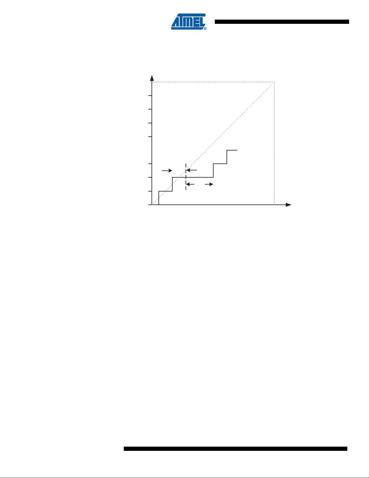
ATtiny4/5/9/10
• Diffe rential Non-linearity (DNL): The ma ximum de viation o f the actual code width (the in terval
ADCL
V
IN
256⋅
V
CC
---------------------- -=
between two adjacent transitions) from the ideal code width (1 LSB). Ideal value: 0 LSB.
Figure 13-12. Differential Non-linearity (DNL)
Output Code
0xFF
1 LSB
DNL
0x00
• Quantization Error: Due to the quantization of the input v olta ge into a finit e numbe r of codes,
a range of input voltages (1 LSB wide) will code to the same value. Always ± 0.5 LSB.
• Absolute Accuracy: The maxim um de viat ion of an actu al (unadju sted) tr ansition compar ed to
an ideal transition for any code. This is the compound effect of offset, gain error, dif ferential
error, non-linearity, and quantization error. Ideal value: ± 0.5 LS B.
13.11 ADC Conversion Result
After the conversion is complete (ADIF is high), the conversion result can be found in the ADC
Data Register (ADCL). For single ended conversion, the result is
where V
voltage reference. 0x00 represents analog ground, and 0xFF represents the selected reference
voltage minus one LSB.
(see Table 13-2 on page 93) is the voltage on the selected input pin and VCC is the
IN
0
V
REF
Input Voltage
92
8127B–AVR–08/09
Page 93

13.12 Register Description
13.12.1 ADMUX – ADC Multiplexer Selection Register
Bit 76543210
0x1B
Read/WriteRRRRRRR/WR/W
Initial Value00000000
• Bits 7:2 – Res: Reserved Bits
These bits are reserved and will always read zero.
• Bits 1:0 – MUX1:0: Analog Channel Selection Bits
The value of these bits selects which combination of analog inputs are connected to the ADC.
See Table 13-2 for details.
in effect until the conversion is complete (ADIF in ADCSRA is set).
Table 13-2. Input Channel Selections
MUX1 MUX0 Single Ended Input
– – – – – – MUX1 MUX0 ADMUX
If these bits are changed during a conversion, the change will not go
ATtiny4/5/9/10
13.12.2 ADCSRA
0
0 ADC0 (PB0)
1 ADC1 (PB1)
0 ADC2 (PB2)
1
1 ADC3 (PB3)
– ADC Control and Status Register A
Bit 76543210
0x1D ADEN ADSC ADATE ADIF ADIE ADPS2 ADPS1 ADPS0 ADCSRA
Read/Write R/W R/W R/W R/W R/W R/W R/W R/W
Initial Value 0 0 0 0 0 0 0 0
• Bit 7 – ADEN: ADC Enable
Writing this bit to one enables the ADC. By writing it to zero, the ADC is turned off. Turning the
ADC off while a conversion is in progress, will terminate this conversion.
• Bit 6 – ADSC: ADC Start Conversion
In Single Conversion mode, write this bit to one to start ea ch conversion. In Free Ru nning mode,
write this bit to one to start the first conver sion. The f irst con version aft er ADSC has bee n written
after the ADC has been enabled, or if ADSC is written at the same time as the ADC is enabled,
will take 25 ADC clock cycles instead of the normal 13. This first conversion performs initialization of the ADC.
8127B–AVR–08/09
ADSC will read as one as long as a conversion is in progress. When the conversion is complete,
it returns to zero. Writing zero to this bit ha s no effect.
• Bit 5 – ADATE: ADC Auto Trigger Enable
When this bit is written to one, Auto Triggering of the ADC is enabled. The ADC will start a conversion on a positive edge of the selected trigger signal. The trigger source is selected by setting
the ADC Trigger Select bits, ADTS in ADCSRB.
93
Page 94

ATtiny4/5/9/10
• Bit 4 – ADIF: ADC Interrupt Flag
This bit is set when an ADC conversion comple tes and t he data reg iste rs ar e upd at ed. Th e ADC
Conversion Complete Interrupt is requested if the ADIE bit is set. ADIF is cleared by hardware
when executing the corresponding interrupt handling vector. Alternatively, ADIF is cleared by
writing a logical one to the flag.
• Bit 3 – ADIE: ADC Interrupt Enable
When this bit is written to one, the ADC Conversion Complete Interrupt request is enabled.
• Bits 2:0 – ADPS2:0: ADC Prescaler Select Bits
These bits determine the division factor between the system clock frequency and th e inpu t clock
to the ADC.
Table 13-3. ADC Prescaler Selections
ADPS2 ADPS1 ADPS0 Division Factor
000 2
001 2
010 4
011 8
100 16
101 32
110 64
111 128
13.12.3 ADCSRB
– ADC Control and Status Register B
Bit 76543210
0x1C
Read/Write R R R R R R/W R/W R/W
Initial Value 0 0 0 0 0 0 0 0
• Bits 7:3 – Res: Reserved Bits
These bits are reserved and will always read zero.
• Bits 2:0 – ADTS2:0: ADC Auto Trigger Source
If ADATE in ADCSRA is written to one, the value of these bits selects which source will trigger
an ADC conversion. If ADATE is cleared, the ADTS2:0 settings will have no effect. A conversion
will be triggered by the rising edge of the selected Interrupt Flag. Note that switching from a trigger source that is cleared to a trigger source that is set, will generate a positive edge on the
– – – – – ADTS2 ADTS1 ADTS0 ADCSRB
94
8127B–AVR–08/09
Page 95

trigger signal. If ADEN in ADCSRA is set, this will start a conversion. Switching to Free Running
mode (ADTS[2:0]=0) will not cause a trigger event, even if the ADC Interrupt Flag is set
Table 13-4. ADC Auto Trigger Source Selections
ADTS2 ADTS1 ADTS0 Trigger Source
0 0 0 Free Running mode
0 0 1 Analo g Comparator
0 1 0 External Interrupt Flag 0
0 1 1 Timer/Counter 0 Compare Match A
1 0 0 Timer/Counter 0 Overflow
1 0 1 Timer/Counter 0 Compare Match B
1 1 0 Pin Change Interrupt 0 Request
1 1 1 Timer/Counter 0 Capture Event
13.12.4 ADCL – ADC Data Register
Bit 76543210
0x19 ADC7 ADC6 ADC5 ADC4 ADC3 ADC2 ADC1 ADC0 ADCL
Read/WriteRRRRRRRR
Initial Value00000000
ATtiny4/5/9/10
.
13.12.5 DIDR0
When an ADC conversion is complete, the result is found in the ADC re gis ter .
• Bits 7:0 – ADC7:0: ADC Conversion Result
These bits represent the result from the conversion.
– Digital Input Disable Register 0
Bit 765432 1 0
0x17 – – – – ADC3D ADC2D ADC1D ADC0D DIDR0
Read/Write R R R R R/W R/W R/W R/W
Initial Value 0 0 0 0 0 0 0 0
• Bits 7:4 – Res: Reserved Bit
These bits are reserved and will always read zero.
• Bits 3:0 – ADC3D..ADC0D: ADC3..0 Digital Input Disable
When this bit is written logic one, the digital input buffer on the corresponding ADC pin is disabled. The corresponding PIN register bit will always read as zero when this bit is set. When an
analog signal is applied to the ADC3..0 pin and the digital input from this pin is not needed, this
bit should be written logic one to reduce power consumption in the digital input buffer.
8127B–AVR–08/09
95
Page 96

ATtiny4/5/9/10
14. Programming interface
T
14.1 Features
• Physical Layer:
– Synchronous Data Transfer
– Bi-directional, Half-duplex Receiver And Transmitter
– Fixed Frame Format With One Start Bit, 8 Data Bits, One Parity Bit And 2 Stop Bits
– Parity Error Detection, Frame Error Detection And Break Character Detection
– Parity Generation And Collision Detection
– Automatic Guard Time Insertion Between Data Reception And Transmission
• Access Layer:
– Communication Based On Messages
– Automatic Exception Handling Mechanism
– Compact Instruction Set
– NVM Programming Access Control
– Tiny Programming Interface Control And Status Space Access Control
– Data Space Access Control
14.2 Overview
The Tiny Programming Interface (TPI) supports external prog ramming of all Non-Volatile Me mories (NVM). Memory programming is done via the NVM Controller, by executing NVM controller
commands as described in “Memory Programming” on page 107.
The Tiny Programming Interface (TPI) provides access to the programming facilities. The interface consists of two layers: the access layer and the physical layer. The layers are illustrated in
Figure 14-1.
Figure 14-1. The Tiny Programming Interface and Related Internal Interfaces
TINY PROGRAMMING INTERFACE (TPI)
RESET
TPICLK
PIDATA
PHYSICAL
LAYER
Programming is done via the physical interface. This is a 3-pin interface, which uses the RESET
pin as enable, the TPICLK pin as the clock input, and the TPIDATA pi n as data inp ut and o utput.
NVM can be programmed at 5V, only.
14.3 Physical Layer of Tiny Programming Interface
The TPI physical layer handles the basic low-level serial communication. The TPI physical layer
uses a bi-directional, half-duplex serial receiver and transmitter. The physical layer includes
serial-to-parallel and parallel-to-serial data conversion, start-of-frame detection, frame error
detection, parity error detection, parity generation and collision detection.
ACCESS
LAYER
NVM
CONTROLLER
NON-VOLATILE
MEMORIES
DATA BUS
96
8127B–AVR–08/09
Page 97

The TPI is accessed via three pins, as follows:
ATtiny4/5/9/10
TPIDATA/PB0
GND
TPICLK/PB1
PB3/RESET
V
CC
PB2
TPI
CONN
APPLICATION
+5V
ATtiny4/5/9/10
RESET
: Tiny Programming Interface enable input
TPICLK: Tiny Programming Interface clock input
TPIDATA: Tiny Programming Interface data input/output
In addition, the V
and GND pins must be connected between the externa l programmer and t he
CC
device. See Figure 14-2.
Figure 14-2. Using an External Programmer for In-System Programming via TPI
NVM can be programmed at 5V, only. In some designs it may be necessary to protect components that can not tolerate 5V with, for example, series resistors.
14.3.1 Enabling
The following sequence enables the Tiny Programming Interface (see Figure 14-3 fo r guidance):
• Apply 5V between V
and GND
CC
• Depending on the met hod of reset to be used:
– Either: wait t
This will reset the device and enable the TPI physical layer. The RESET
(see Table 16-4 on page 119) and then set the RESET pin low.
TOUT
pin must
then be kept low for the entire programming session
– Or: if the RSTDISBL configuration bit has been programmed, apply 12V to the
RESET
•Wait t
pin. The RESET pin must be kept at 12V f or the entire pr og ra mming session
(see Table 16-4 on page 119)
RST
• Keep the TPIDATA pin high for 16 TPICLK cycles
Figure 14-3. Sequence for enabling the Tiny Programming Interface
16 x TPICLK CYCLES
RESET
TPICLK
TPIDATA
t
RST
8127B–AVR–08/09
97
Page 98

ATtiny4/5/9/10
14.3.2 Disabling
TPIDATA
TPICLK
SP1ST SP2 IDLE/STIDLE PD1D0 D7
14.3.3 Frame Format
Provided that the NVM enable bit has been cleared, the TPI is automatically disabled if the
RESET
RESET
pin is released to inactive high state or, alternatively, if VHV is no longer applied to the
pin.
If the NVM enable bit is not cleared a power down is required to exit TPI programming mode.
See NVMEN bit in “TPISR – Tiny Programming Interface Status Register” on page 106.
The TPI physical layer supports a fixed frame format. A frame consists of one character, eight
bits in length, and one start bit, a parity bit and two stop bits. Data is transferred with the least
significant bit first.
Figure 14-4. Serial frame format.
Symbols used in Figure 14-4:
ST: Start bit (always low)
D0-D7: Data bits (least significant bit sent first)
P: Parity bit (using even parity)
SP1: Stop bit 1 (always high)
SP2: Stop bit 2 (always high)
14.3.4 Parity Bit Calculation
The parity bit is always calculated using even parity. The value of the bit is calculated by doing
an exclusive-or of all the data bits, as follows:
where:
14.3.5 Supported Characters
The BREAK character is equal to a 12 bit long low level. It can be extended beyond a bit-length
of 12.
Figure 14-5. Supported characters.
TPIDATA
TPIDATA
P = D0
⊗ D1 ⊗ D2 ⊗ D3 ⊗ D4 ⊗ D5 ⊗ D6 ⊗ D7 ⊗ 0
P: Parity bit using even parity
D0-D7: Data bits of the ch ar ac te r
DATA CHARACTER
BREAK CHARACTER
SP1ST SP2 IDLE/STIDLE PD1D0 D7
IDLE/STIDLE
98
8127B–AVR–08/09
Page 99

14.3.6 Operation
TPIDATA
TPICLK
SAMPLE
SETUP
ATtiny4/5/9/10
The TPI physical layer operates synchronously on the TPICLK provided by the external programmer. The dependency between the clock edges and data sampling or data change is
shown in Figure 14-6. Data is changed at falling edges and sampled at rising edges.
Figure 14-6. Data changing and Data sampling.
The TPI physical layer supports two modes of operation: Transmit and Receive. By default, the
layer is in Receive mode, waiting for a start bit. The mode of operation is controlled by the
access layer.
14.3.7 Serial Data Reception
When the TPI physical layer is in receive mode, data reception is started as soon as a start bit
has been detected. Each bit that follows the start bit will be sampled at the rising edge of the
TPICLK and shifted into the shift register until the second stop bit has been received. When the
complete frame is present in the shift register the received data will be available for the TPI
access layer.
There are three possible exceptions in the receive mode: frame error, parity error and break
detection. All these exceptions are signalized to the TPI access layer, which then enters the
error state and puts the TPI physical layer into receive mode, waiting for a BREAK character.
• Frame Error Exception. The frame error exception indicates the state of the stop bit. The
frame error exception is set if the stop bit was read as zero.
• Parity Error Exception. The parity of the data bits is calculated during the frame reception.
After the frame is received completely, the result is compared with the parity bit of the frame .
If the comparison fails the parity error exception is signalized.
• Break Detection Exception. Th e Break detection e xception is giv en when a complete f rame of
all zeros has been received.
14.3.8 Serial Data Transmission
When the TPI physical layer is ready to send a new frame it initiates data transmission by loading the shift register with the d ata to be transm itted. Wh en the sh ift reg ister h as been loaded with
new data, the transmitter shifts on e co m plete fr am e ou t on th e TPIDATA line at the transfer rate
given by TPICLK.
If a collision is detected during transmission, the output driver is disabled. The TPI access layer
enters the error state and the TPI physical layer is put into receive mode, waiting for a BREAK
character.
99
8127B–AVR–08/09
Page 100

ATtiny4/5/9/10
14.3.9 Collision Detection Exception
The TPI physical layer uses one bi-directio nal data line for both data recep tion and tra nsmission.
A possible drive contention may occur, if the external programmer and the TPI physical layer
drive the TPIDATA line simultaneously. In order to reduce the effect of the drive contention, a
collision detection mechanism is supported. The collision detection is based on the way the TPI
physical layer drives the TPIDATA line.
The TPIDATA line is driven by a tri-state, push-pull driver with internal pull-up. The output driver
is always enabled when a logical zero is sent. When sending successive logical ones, the output
is only driven actively during the first clock cycle. After this, the output driver is automatically tristated and the TPIDATA line is kept high by the internal pull-up. The output is re-enabled, when
the next logical zero is sent.
The collision detection is enabled in transmit mode, when the output driver has been disabled.
The data line should now be kept high by the internal pull-up and it is monitored to see, if it is
driven low by the external programmer. If the output is read low, a collision has been detected.
There are some potential pit-falls related to the way collision detection is performed. For example, collisions cannot be detected when the TPI physical layer transmits a bit-stream of
successive logical zeros, or bit-stream of alternating logical ones and zeros. This is because the
output driver is active all the time, preventing polling of the TPIDATA line. However, within a single frame the two stop bits should always be transmitted as logical ones, enabling collision
detection at least once per frame (as long as the frame format is not violated regarding the stop
bits).
The TPI physical layer will cease transmission when it detects a collision on the TPIDATA line.
The collision is signalized to the TPI access layer, which immediately changes the physical layer
to receive mode and goes to the error state. The TPI access layer can be recovered from the
error state only by sending a BREAK character.
14.3.10 Direction Change
In order to ensure correct timing of the half-duplex operation, a simple guard time mechanism
has been added to the physical layer. When the TPI physical layer changes from receive to
transmit mode, a configurable number of additional IDLE bits are inserted before the start bit is
transmitted. The minimum transition time between receive and transmit mode is two IDLE bits.
The total IDLE time is the specified guard time plus two IDLE bits.
The guard time is configured by dedicated bits in the TPIPCR register. The default guard time
value after the physical layer is initialized is 128 bits.
The external programmer looses control of the TPIDATA line when the TPI target changes from
receive mode to transmit. The guard time feature relaxes this critical phase of the communication. When the external programmer changes from receive mode to transmit, a minimum of one
IDLE bit should be inserted before the start bit is transmitted.
14.4 Access Layer of Tiny Programming Interface
The TPI access layer is responsible for handling the communication with the external programmer. The communication is based on message format, where each message comprises an
instruction followed by one or more byte-sized operands. The instruction is always sent by the
external programmer but operands are sent either by the external programmer or by the TPI
access layer, depending on the type of instruction issued.
100
8127B–AVR–08/09
 Loading...