

Page 1

Features
• 405 nm, 650 nm and 780 nm Wavelengths Supported
• Blu-ray/HD-DVD x5, CD-R/RW x52, DVD-R/RW x16
• Adjustment of Mode and Gain by Setting Internal Register via Two-wire Interface (TWI)
• 200 MHz Channel Bandwidth
• Paraphase Outputs
• Internal Reference Voltage Generation
• Fast Settling Time
• Low Offset Voltage
• Power-down Mode
• Pb-free Optical 12-pin Package
Front Monitor
Diode for
Applications
• Blu-ray/HD-DVD
• DVD+RW with CD-RW Capability
• DVD-RW with CD-RW Capability
• DVD-RAM with CD-RW Capability
• Recordable Optical Data Storage Devices
1. Description
The ATR1841 is a front monitor diode (FMD) which controls the laser power of the
optical pickup for Blu-ray/HD-DVD, DVD and CD drives in one IC.
With the Two-wire Interface (TWI) it is possible to fit the laser power for
Blu-ray/HD-DVD, DVD and CD. Two bits are used to set the mode/gain level and 6
additional bits are used for gain trimming, within ±6 dB. Entering sleep mode is also
controlled via the TWI.
The integrated PIN diode and the high speed amplifier with low output impedance
ensures stable driver performance.
All output channels are set to tri-state during sleep mode.
Due to its small package size the ATR1841 is especially suited for applications with
low height requirements like SLIM and Ultra-SLIM drives.
Blu-ray/HD-DVD/
DVD/CD with
TWI
ATR1841
Summary
Preliminary
NOTE: This is a summary document.
The complete document is currently not
available. For more information, please
contact your local Atmel sales office.
9103AS–DVD–08/07
Page 2
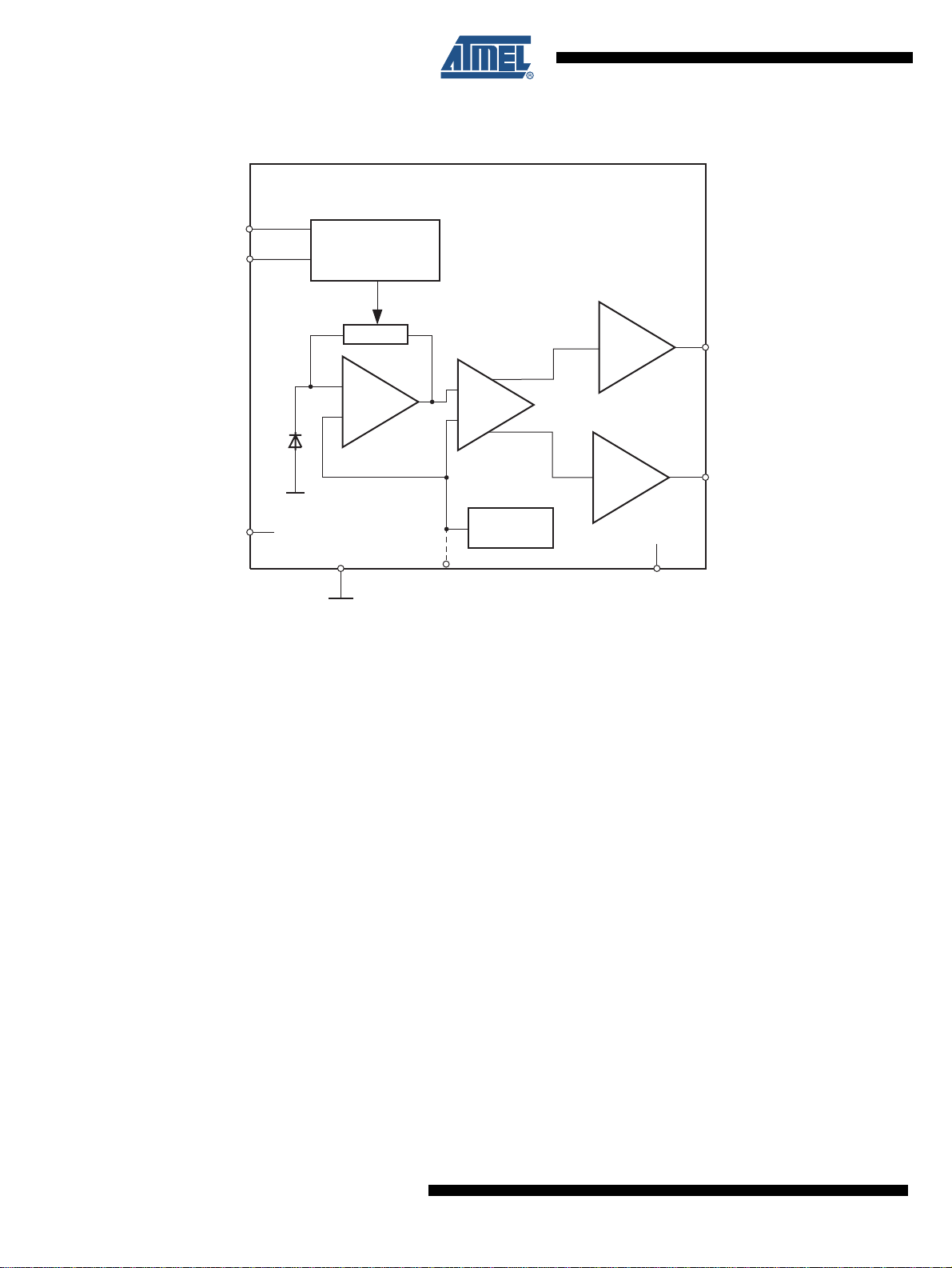
Figure 1-1. Block Diagram
SDA
SCL
VCC
Gain Select (H/M/L)
Gain Adjust (±6 dB)
GND
RF+
RF-
Internal
Vref
ADS
2
ATR1841 [Preliminary]
9103AS–DVD–08/07
Page 3
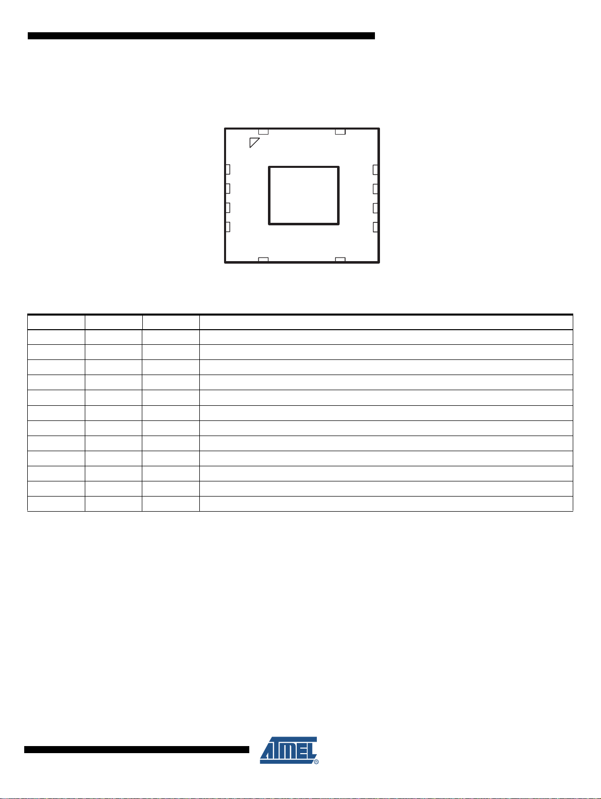
2. Pin Configuration
Figure 2-1. Pinning QFN12L
ATR1841 [Preliminary]
NC NC
10 11
GND
RF-
RF+
VCC
Table 2-1. Pin Description
Pin Symbol Type Function
1 GND Supply Ground
2 RF- Analog Negative output
3 RF+ Analog Positive output
4 VCC Supply Power supply
5SDADigital
6 SCL Digital
7ADSAnalog
8 GND Supply Ground
9 NC Not connected
10 NC Not connected
11 NC Not connected
12 NC Not connected
TWI serial data
TWI serial clock
TWI slave address select
1
2
3
4
912
NC NC
GND
8
ADS
7
SCL
6
SDA
5
9103AS–DVD–08/07
3
Page 4

3. Absolute Maximum Ratings
Stresses beyond those listed under “Absolute Maximum Ratings” may cause permanent damage to the device. This is a stress rating
only and functional operation of the device at these or any other conditions beyond those indicated in the operational sections of this
specification is not implied. Exposure to absolute maximum rating conditions for extended periods may affect device reliability.
Parameters Symbol Value Unit
Supply voltage V
Input voltage at any input V
Storage temperature T
Soldering temperature QFN_Open package T
CC
in
stg
sol
–0.5 to +6.0 V
–0.5 to VCC – 0.5 V
–40 to +100 °C
260 °C
4. Recommended Operating Conditions
Parameters Symbol Value Unit
Supply voltage V
Operating temperature range T
CC
amb
4.5 to 5.5 V
–10 to +80 °C
5. Electrical Characteristics: General
VCC = 5V, T
Output load: R
No. Parameters Test Conditions Pin Symbol Min. Typ. Max. Unit Type*
1 DC Specifications, Power Supply
1.1 Supply current I
1.2
1.3 V
1.4 TCV
1.5 Maximum output voltage V
1.6 Minimum output voltage V
1.7
1.8
2 Output Offset Voltage
2.1 Output offset V
2.2 Offset drift dV
*) Type means: A = 100% tested, B = 100% correlation tested, C = Characterized on samples, D = Design parameter
= 25°C, λ = 405 nm/780 nm/650 nm
amb
= 10 kΩ, C
load
= 20 pF
load
Supply current
(standby mode)
REF_INT
REF_INT
Power supply rejection
ratio
Power supply rejection
ratio
Low-frequency (10 kHz),
inclusive application/
flexboard
High-frequency
(100 kHz), inclusive
application/ flexboard
REF
– V
RF+
, V
REF
– V
RF–
CC
I
CC
28 30 mA A
0.5 mA A
1.65 V A
15 µV/°C C
out
out
VCC –
0.9
0.3 V C
VC
PSRR –45 dB C
PSRR –45 dB C
V
OFF1
/dT –25 +25 µV/°C C
OFF
–20 0 +20 mV C
4
ATR1841 [Preliminary]
9103AS–DVD–08/07
Page 5

6. Two-wire Interface (TWI)
6.1 Slave Address
MSB (ADS) LSB
0 01110 0 R/W = 0 Pin ADS = low (GND)
0 01110 1 R/W = 0 Pin ADS = high (V
6.2 Data
MSB LSB
m1 m2 g1 g2 g3 g4 g5 g6
6.3 Mode Setting
The first two bits select the mode/gain level.
ATR1841 [Preliminary]
)
CC
6.4 Gain Setting
Table 6-1. Mode Selection Register
m1 m2 Mode Select
1 1 High gain
1 0 Middle gain
0 1 Low gain
00 Sleep
The last six bits are used to finely adjust the gain by ±6 dB
Table 6-2. Gain Selection Register
g1 g2 g3 g4 g5 g6 Gain
111111 +6dB
……
100000 0dB
……
000000 –6dB
9103AS–DVD–08/07
5
Page 6

7. Applications Recommendation
To achieve the best performance VCC needs to be blocked using a high quality capacitor
(C = 100 nF) as close to IC/pin as possible.
8. Photo Diode Arrangement
Figure 8-1. Phote Diode Arrangement
Dimensions
D 500.0 µm
Photo diode is symmetrically centered
to the center of the chip and package
D
6
ATR1841 [Preliminary]
9103AS–DVD–08/07
Page 7

ATR1841 [Preliminary]
9. Ordering Information
Extended Type Number Package Remarks
ATR1841-P1QN QFN_OPEN_3x3_8L Taped and reeled, Pb-free
10. Package Information
9103AS–DVD–08/07
7
Page 8

Headquarters International
Atmel Corporation
2325 Orchard Parkway
San Jose, CA 95131
USA
Tel: 1(408) 441-0311
Fax: 1(408) 487-2600
Atmel Asia
Room 1219
Chinachem Golden Plaza
77 Mody Road Tsimshatsui
East Kowloon
Hong Kong
Tel: (852) 2721-9778
Fax: (852) 2722-1369
Product Contact
Web Site
www.atmel.com
Literature Requests
www.atmel.com/literature
Atmel Europe
Le Krebs
8, Rue Jean-Pierre Timbaud
BP 309
78054
Saint-Quentin-en-Yvelines Cedex
France
Tel: (33) 1-30-60-70-00
Fax: (33) 1-30-60-71-11
Technical Support
dvd_ldd@atmel.com
Atmel Japan
9F, Tonetsu Shinkawa Bldg.
1-24-8 Shinkawa
Chuo-ku, Tokyo 104-0033
Japan
Tel: (81) 3-3523-3551
Fax: (81) 3-3523-7581
Sales Contact
www.atmel.com/contacts
Disclaimer: The information in this document is provided in connection with Atmel products. No license, express or implied, by estoppel or otherwise, to any
intellectual property right is granted by this document or in connection with the sale of Atmel products. EXCEPT AS SET FORTH IN ATMEL’S TERMS AND CONDI-
TIONS OF SALE LOCATED ON ATMEL’S WEB SITE, ATMEL ASSUMES NO LIABILITY WHATSOEVER AND DISCLAIMS ANY EXPRESS, IMPLIED OR STATUTORY
WARRANTY RELATING TO ITS PRODUCTS INCLUDING, BUT NOT LIMITED TO, THE IMPLIED WARRANTY OF MERCHANTABILITY, FITNESS FOR A PARTICULAR
PURPOSE, OR NON-INFRINGEMENT. IN NO EVENT SHALL ATMEL BE LIABLE FOR ANY DIRECT, INDIRECT, CONSEQUENTIAL, PUNITIVE, SPECIAL OR INCIDENTAL D AMAGES (INCLUDING, WITHOUT LIMITATION, DAMAGES FOR LOSS OF PROFITS, BUSINESS INTERRUPTION, OR LOSS OF INFORMATION) ARISING OUT OF
THE USE OR INABILITY TO USE THIS DOCUMENT, EVEN IF ATMEL HAS BEEN ADVISED OF THE POSSIBILITY OF SUCH DAMAGES. Atmel makes no
representations or warranties with respect to the accuracy or completeness of the contents of this document and reserves the right to make changes to specifications
and product descriptions at any time without notice. Atmel does not make any commitment to update the information contained herein. Unless specifically provided
otherwise, Atmel products are not suitable for, and shall not be used in, automotive applications. Atmel’s products are not intended, authorized, or warranted for use
as components in applications intended to support or sustain life.
© 2007 Atmel Corporation. All rights reserved. Atmel®, logo and combinations thereof, and others are registered trademarks or trademarks of
Atmel Corporation or its subsidiaries. Other terms and product names may be trademarks of others.
9103AS–DVD–08/07
 Loading...