

Page 1

Features
• 16-channel GPS Correlator
– 8192 Search Bins with GPS Acquisition Accelerator
– Accuracy: 2.5m CEP (2D, Stand Alone)
– Time to First Fix: 34s (Cold Start)
– Acquisition Sensitivity: –142 dBm (Cold Start, With External LNA)
– Tracking Sensitivity: –158 dBm (With External LNA)
• Utilizes the ARM7TDMI
– High-performance 32-bit RISC Architecture
– EmbeddedICE
• 128 Kbytes Internal RAM
• 384 Kbytes Internal ROM with u-blox GPS Firmware SuperSense
• 1.5-bit ADC On-chip
• Single IF Architecture
• 2 External Interrupts
• 24 User-programmable I/O Lines
• 1 USB Device Port
– Universal Serial Bus (USB) 2.0 Full-speed Device
– Embedded USB V2.0 Full-speed Transceiver
• 2 USARTs
• Master/Slave SPI Interface
– 4 External Slave Chip Selects
• Programmable Watchdog Timer
• Advanced Power Management Controller (APMC)
– Geared Master Clock to Reduce Power Consumption
– Sleep State with Disabled Master Clock
– Hibernate State with 32.768 kHz Master Clock
• Real Time Clock (RTC)
• 1.8V to 3.3V User-definable IO Voltage for Several GPIOs with 5V Tolerance
• 4 KBytes of Battery Backup Memory
• 7 mm × 10 mm 96 Pin BGA Package, 0.8 mm Pitch, Pb-free, RoHS-compliant
®
ARM® Thumb® Processor Core
™
(In-Circuit Emulation)
®
ANTARIS4
Single-chip
GPS Receiver
SuperSense
ATR0635P1
Automotive
Benefits
• Fully Integrated Design With Low BOM
• No External Flash Memory Required
• Supports NMEA
• Supports SBAS (WAAS, EGNOS, MSAS)
• Up to 4 Hz Update Rate
• Supports A-GPS (Aiding)
• Excellent Noise Performance
®
, UBX Binary and RTCM Protocol for DGPS
4979D–GPS–06/08
Page 2

1. Description
The ATR0635P1 is a low-power, single-chip GPS receiver, especially designed to meet the
requirements of mobile applications. It is based on Atmel
grates an RF front-end, filtering, and a baseband processor in a single, tiny 7 mm × 10 mm
96 pin BGA package. Providing excellent RF performance with low noise figure and low power
consumption.
Due to the fully integrated design, just an RF SAW filter, a GPS TCXO and blocking capacitors
are required to realize a stand-alone GPS functionality.
The ATR0635P1 includes a complete GPS firmware, licensed from u-blox AG, which performs
the GPS operation, including tracking, acquisition, navigation and position data output. For normal PVT (Position/Velocity/Time) applications, there is no need for external Flash- or
ROM-memory.
The firmware supports e.g. the NMEA protocol (2.1 and 2.3), a binary protocol for PVT data,
configuration and debugging, the RTCM protocol for DGPS, SBAS (WAAS, EGNOS and MSAS)
and A-GPS (aiding). It is also possible to store the configuration settings in an optional external
EEPROM.
Due to the integrated ARM7TDMI processor and an intelligent radio architecture, the
ATR0635P1 operates in a complete autonomous mode, utilizing on chip AGC in closed loop
operation.
For maximum performance, we recommend to use the ATR0635P1 together with a low noise
amplifier (e.g. ATR0610).
®
’s ANTARIS®4 technology and inte-
The ATR0635P1 supports assisted GPS.
2
ATR0635P1
4979D–GPS–06/08
Page 3
2. Architectural Overview
NSLEEP
NSHDN
XT_IN
TMS
TCK
TDO
TDI
NTRST
DBG_EN
P25/NAADET0
P14/NAADET1
P31/RXD1
P18/TXD1
AGCO
SIGHI
EGC
SDI
CLK23
SIGLO
P22/RXD2
P21/TXD2
P8/STATUSLED
P2/BOOT_MODE
P16/NEEPROM
P30/AGCOUT0
LDO_EN
LDO_IN
LDO_OUT
LDOBAT_IN
VBAT
P1/GPSMODE0
VBP
VCC2
VCC1
VDD_USB
VDDIO
VDD18
PURF
PUXTO
VDIG
P12/GPSMODE2
P13/GPSMODE3
P17/GPSMODE5
P23/GPSMODE7
P24/GPSMODE8
P26/GPSMODE10
P27/GPSMODE11
P29/GPSMODE12
P19/GPSMODE6
P0/NANTSHORT
P15/ANTON
P9/EXTINT0
VBAT18
XT_OUT
P20/TIMEPULSE
USB_DM
NRESET
USB_DP
Embedded
ICE
ARM7TDMI
USART1 USART2
PIO2
SPIUSB
ASB APB
PDC2
B
RID
G
E
ROM
384K
USB
Transceiver
SRAM
128K
Watchdog
JTAG
PIO2
Reset
Controller
Interface to
Off-Chip
Memory
(EBI)
Advanced
Interrupt
Controller
GPS
Accelerator
Timer
Counter
GPS
Correlators
SMD
Generator
MO
TEST
Power Supply Manager/
PMSS/Logic
NXTO
XTO
NX
X
RF_ON
VCO
PLL
XTO
Advanced
Power
Manage-
ment
Controller
SRAM
RTC
PIO2
Controller
Special
Function
1
D
A
D
A
NRF
RF
2.1 Block Diagram
Figure 2-1. ATR0635P1 Block Diagram
ATR0635P1
4979D–GPS–06/08
3
Page 4

2.2 General Description
The ATR0635P1 has been designed especially for mobile applications. It provides high isolation
between GPS and cellular bands, as well as very low power consumption.
ATR0635P1 is based on the successful ANTARIS4 technology which includes the ANTARIS
high performance SuperSense software in ROM, developed by u-blox AG, Switzerland. ANTARIS provides a proven navigation engine which is used in high-end car navigation systems,
automatic vehicle location (AVL), security and surveying systems, traffic control, road pricing,
and speed camera detectors, and provides location-based services (LBS) worldwide.
The ANTARIS4 chipset has a very low power consumption and comes with a very low BoM for
the passive components. Also, as the high performance software SuperSense is available in
ROM, no external flash memory is needed.
The L1 input signal (f
quency of 1575.42 MHz. The digital modulation scheme is Bi-Phase-Shift-Keying (BPSK) with a
chip rate of 1.023 Mbps.
2.3 PMSS Logic
The power management, startup and shutdown (PMSS) logic ensures reliable operation within
the recommended operating conditions. The external power control signals PUrf and PUxto are
passed through Schmitt trigger inputs to eliminate voltage ripple and prevent undesired behavior
during start-up and shut-down. Digital and analog supply voltages are analyzed by a monitoring
circuit, enabling the startup of the IC only when it is within a safe operating range.
2.4 VCO/PLL
The frequency synthesizer features a balanced VCO and a fully integrated loop filter, thus no
external components are required. The VCO combines very good phase noise behavior and
excellent spurious suppression.The relation between the reference frequency (f
VCO center frequency (f
f
VCO=fTCXO
2.5 RF Mixer/Image Filter
Combined with the antenna, an external LNA provides a first band-path filtering of the signal.
Atmel’s ATR0610 is recommended for the LNA due to its low noise figure, high linearity and low
power consumption. The output of the LNA drives a SAW filter, which provides image rejection
for the mixer and the required isolation to all GSM bands. The output of the SAW filter is fed into
a highly linear mixer with high conversion gain and excellent noise performance.
) is a Direct Sequence Spread Spectrum (DSSS) signal with a center fre-
RF
) is given by:
TCXO
× 64 = 23.104 MHz × 64 = 1478.656 MHz.
TCXO
) and the
2.6 VGA/AGC
4
ATR0635P1
The on-chip automatic gain control (AGC) stage sets the gain of the VGA in order to optimally
load the input of the following analog-to-digital converter. The AGC control loop can be selected
for on-chip closed-loop operation or for baseband controlled gain mode.
4979D–GPS–06/08
Page 5

2.7 Analog-to-digital Converter
The analog-to-digital converter stage has a total resolution of 1.5 bits. It comprises balanced
comparators and a sub-sampling unit, clocked by the reference frequency (f
quency spectrum of the digital output signal (f
SIGH1, is 4.348 MHz.
2.8 Baseband
The GPS baseband core includes a 16-channel correlator and is based on an ARM7TDMI ARM
processor core with very low power consumption. It has a high-performance 32 bit RISC architecture, uses a high-density 16-bit instruction set. The ARM standard In-Circuit Emulation debug
interface is supported via the JTAG/ICE port of the ATR0635P1.
The ATR0635P1 architecture consists of two main buses, the Advanced System Bus (ASB) and
the Advanced Peripheral Bus (APB). The ASB is designed for maximum performance. It interfaces the processor with the on-chip 32-bit memories and the external memories and devices by
means of the External Bus Interface (EBI). The APB is designed for accesses to on-chip peripherals and is optimized for low power consumption. The AMBA
between the ASB and the APB.
An on-chip Peripheral Data Controller (PDC2) transfers data between the on-chip USARTs/SPI
and the on- and off-chip memories without processor intervention. Most importantly, the PDC2
removes the processor interrupt handling overhead and significantly reduces the number of
clock cycles required for a data transfer. It can transfer up to 64K contiguous bytes without
reprogramming the starting address. As a result, the performance of the microcontroller is
increased and the power consumption reduced.
ATR0635P1
). The fre-
TCXO
), present at the data outputs SIGLO and
OUT
™
Bridge provides an interface
All of the external signals of the on-chip peripherals are under the control of the Parallel I/O Controller (PIO2). The PIO2 Controller can be programmed to insert an input filter on each pin or
generate an interrupt on a signal change. After reset, the user must carefully program the PIO2
Controller in order to define which peripheral signals are connected with off-chip logic.
The ATR0635P1 features a Programmable Watchdog Timer.
An Advanced Power Management Controller (APMC) allows for the peripherals to be deactivated individually. Automatic master clock gearing reduces power consumption. A Sleep Mode
is available with disabled 23.104 MHz master clock, as well as a Back-up Mode operating
32.768 kHz master clock.
A 32.768 kHz Real Time Clock (RTC), together with a buit-in battery back-up SRAM, allows for
storage of Almanac, Ephemeris, software configurations to make quick hot- and warm starts.
The ATR0635P1 includes the full high performance firmware (SuperSense), licensed from
u-blox AG, Switzerland. Features of the ROM firmware are described in a software documentation available from u-blox AG, Switzerland.
4979D–GPS–06/08
5
Page 6
3. Pin Configuration
3.1 Pinout
Figure 3-1. Pinning BGA96 (Top View)
123456789101112
A
B
C
D
E
F
G
H
ATR0635P1
Table 3-1. ATR0635P1 Pinout
Pull Resistor
Pin Name BGA 96 Pin Type
AGCO A4 Analog I/O
CLK23 A8 Digital OUT
DBG_EN E8 Digital IN PD
EGC D4 Digital IN
GDIG C5 Supply
GND A6 Supply
GND A9 Supply
GND B11 Supply
GND F5 Supply
GND H8 Supply
GND H12 Supply
GNDA A3 Supply
GNDA B1 Supply
Notes: 1. PD = internal pull-down resistor, PU = internal pull-up resistor, OH = switched to Output High at reset
2. VBAT18 represent the internal power supply of the backup power domain, see section “Power Supply” on page 20.
3. VDD_USB is the supply voltage for following the USB pins: USB_DM and USB_DP, see section “Power Supply” on page
20. For operation of the USB interface, supply of 3.0V to 3.6V is required.
4. VDDIO is the supply voltage for the following GPIO pins: P1, P2, P8, P12, P14, P16, P17, P18, P19, P20, P21, P23, P24,
P25, P26, P27 and P29, see section “Power Supply” on page 20.
(Reset Value)
(1)
Firmware Label
PIO Bank A
IO
6
ATR0635P1
4979D–GPS–06/08
Page 7

ATR0635P1
Table 3-1. ATR0635P1 Pinout (Continued)
Pull Resistor
Pin Name BGA 96 Pin Type
GNDA B4 Supply
GNDA D2 Supply
GNDA E1 Supply
GNDA E2 Supply
GNDA E3 Supply
GNDA F1 Supply
GNDA F2 Supply
GNDA F3 Supply
GNDA G1 Supply
GNDA H1 Supply
LDOBAT_IN D11 Supply
LDO_EN C11 Digital IN
LDO_IN E11 Supply
LDO_OUT E12 Supply
MO C3 Analog OUT
NRESET A7 Digital I/O Open Drain PU
NRF C1 Analog IN
NSHDN E9 Digital OUT
NSLEEP E10 Digital OUT
NTRST H11 Digital IN PD
NX B2 Analog OUT
NXTO B3 Analog IN
P0 C8 Digital I/O PD NANTSHORT
P1 D8 Digital I/O Configurable (PD) GPSMODE0
P2 C6 Digital I/O Configurable (PD) BOOT_MODE ‘0’
P8 D7 Digital I/O Configurable (PD) STATUSLED ‘0’
P9 A11 Digital I/O PU to VBAT18 EXTINT0 EXTINT0
P12 D6 Digital I/O Configurable (PU) GPSMODE2 NPCS2
P13 B10 Digital I/O PU to VBAT18 GPSMODE3 EXTINT1
P14 G6 Digital I/O Configurable (PD) NAADET1 ‘0’
P15 F11 Digital I/O PD ANTON
P16 G8 Digital I/O Configurable (PU) NEEPROM
P17 H6 Digital I/O Configurable (PD) GPSMODE5 SCK1 SCK1
P18 C7 Digital I/O Configurable (PU) TXD1 TXD1
P19 F6 Digital I/O Configurable (PU) GPSMODE6
Notes: 1. PD = internal pull-down resistor, PU = internal pull-up resistor, OH = switched to Output High at reset
2. VBAT18 represent the internal power supply of the backup power domain, see section “Power Supply” on page 20.
3. VDD_USB is the supply voltage for following the USB pins: USB_DM and USB_DP, see section “Power Supply” on page
20. For operation of the USB interface, supply of 3.0V to 3.6V is required.
4. VDDIO is the supply voltage for the following GPIO pins: P1, P2, P8, P12, P14, P16, P17, P18, P19, P20, P21, P23, P24,
P25, P26, P27 and P29, see section “Power Supply” on page 20.
(Reset Value)
(1)
Firmware Label
PIO Bank A
IO
4979D–GPS–06/08
7
Page 8

Table 3-1. ATR0635P1 Pinout (Continued)
Pull Resistor
Pin Name BGA 96 Pin Type
P20 G7 Digital I/O Configurable (PD) TIMEPULSE SCK2 SCK2
P21 E6 Digital I/O Configurable (PU) TXD2 TXD2
P22 D10 Digital I/O PU to VBAT18 RXD2 RXD2
P23 F8 Digital I/O Configurable (PU) GPSMODE7 SCK SCK
P24 H7 Digital I/O Configurable (PU) GPSMODE8 MOSI MOSI
P25 G5 Digital I/O Configurable (PD) NAADET0 MISO MISO
P26 B6 Digital I/O Configurable (PU) GPSMODE10 NSS NPCS0
P27 F7 Digital I/O Configurable (PU) GPSMODE11 NPCS1
P28 E7 Digital I/O OH
P29 D5 Digital I/O Configurable (PU) GPSMODE12 NPCS3
P30 G12 Digital I/O PD AGCOUT0 AGCOUT0
P31 C10 Digital I/O PU to VBAT18 RXD1 RXD1
PURF G4 Digital IN
PURF H4 Digital IN
PUXTO F4 Digital IN
RF D1 Analog IN
RF_ON F10 Digital OUT PD
SDI C4 Digital IN
SIGHI0 B8 Digital OUT
SIGLO0 B7 Digital OUT
TCK G9 Digital IN PU
TDI H10 Digital IN PU
TDO F9 Digital OUT
TEST D3 Analog IN
TMS G10 Digital IN PU
USB_DM D9 Digital I/O
USB_DP C9 Digital I/O
VBAT D12 Supply
(2)
VBAT18
VBP G2 Supply
VBP G3 Supply
VBP H2 Supply
VBP H3 Supply
VCC1 C2 Supply
VCC2 E4 Supply
Notes: 1. PD = internal pull-down resistor, PU = internal pull-up resistor, OH = switched to Output High at reset
C12 Supply
2. VBAT18 represent the internal power supply of the backup power domain, see section “Power Supply” on page 20.
3. VDD_USB is the supply voltage for following the USB pins: USB_DM and USB_DP, see section “Power Supply” on page
20. For operation of the USB interface, supply of 3.0V to 3.6V is required.
4. VDDIO is the supply voltage for the following GPIO pins: P1, P2, P8, P12, P14, P16, P17, P18, P19, P20, P21, P23, P24,
P25, P26, P27 and P29, see section “Power Supply” on page 20.
(Reset Value)
(1)
Firmware Label
PIO Bank A
IO
8
ATR0635P1
4979D–GPS–06/08
Page 9
Table 3-1. ATR0635P1 Pinout (Continued)
Pull Resistor
Pin Name BGA 96 Pin Type
VDD_USB
VDD18 H9 Supply
VDD18 G11 Supply
VDD18 F12 Supply
VDD18 B9 Supply
VDD18 E5 Supply
VDDIO
VDDIO H5 Supply
XT_IN A12 Analog IN
XT_OUT B12 Analog OUT
Notes: 1. PD = internal pull-down resistor, PU = internal pull-up resistor, OH = switched to Output High at reset
(3)
A10 Supply
(4)
VDIG A5 Supply
X A2 Analog OUT
XTO A1 Analog Input
2. VBAT18 represent the internal power supply of the backup power domain, see section “Power Supply” on page 20.
3. VDD_USB is the supply voltage for following the USB pins: USB_DM and USB_DP, see section “Power Supply” on page
4. VDDIO is the supply voltage for the following GPIO pins: P1, P2, P8, P12, P14, P16, P17, P18, P19, P20, P21, P23, P24,
B5 Supply
20. For operation of the USB interface, supply of 3.0V to 3.6V is required.
P25, P26, P27 and P29, see section “Power Supply” on page 20.
(Reset Value)
(1)
Firmware Label
PIO Bank A
IO
ATR0635P1
3.2 Signal Description
Table 3-2. Signal Description
Pin Number Pin Name Type Active Level Pin Description/Comment
RF Section
D1 RF ANALOG IN - Input from SAW filter
C1 NRF ANALOG IN - Inverted input from SAW filter
GPS XTAL Section
A1 XTO ANALOG IN - TCXO input (23.104 MHz)
B3 NXTO ANALOG IN - Inverted TCXO input (23.104 MHz)
A2 X ANALOG OUT - XTO interface (capacitor)
B2 NX ANALOG OUT - Inverted XTO interface (capacitor)
RTC Section
A12 XT_IN ANALOG IN - Oscillator input (32.768 kHz)
B12 XT_OUT ANALOG OUT - Oscillator output (32.768 kHz)
Automatic Gain Control, bandwidth setting
A4 AGCO ANALOG IO - Automatic gain control analog voltage, connect shunt capacitor to GND
D4 EGC DIGITAL IN -
G12 AGCOUT0 DIGITAL OUT - Software gain control
C4 SDI DIGITAL IN - Software gain control
Enable external gain control
(high = software gain control, low = automatic gain control)
4979D–GPS–06/08
9
Page 10
Table 3-2. Signal Description (Continued)
Pin Number Pin Name Type Active Level Pin Description/Comment
Boot Section
C6 BOOT_MODE DIGITAL IN - Leave open, internal pull down
Reset
A7 NRESET DIGITAL IN Low Reset input; open drain with internal pull-up resistor
APMC/Power Management
E9 NSHDN DIGITAL OUT Low Shutdown output, connect to LDO_EN (C11)
C11 LDO_EN DIGITAL IN - Enable LDO18
E10 NSLEEP DIGITAL OUT Low Power-up output for GPS XTAL, connect to PUXTO (F4)
F4 PUXTO DIGITAL IN - Power-up input for GPS XTAL
G4, H4 PURF DIGITAL IN - Power-up input for GPS radio
F10 RF_ON DIGITAL OUT - Power-up output for GPS radio, connect to PURF (G4, H4)
Advanced Interrupt Controller (AIC)
A11, B10 EXTINT0-1 DIGITAL IN
USART
C10, D10 RXD1/RXD2 DIGITAL IN - USART receive data
C7, E6 TXD1/TXD2 DIGITAL OUT - USART transmit data
H6, G7 SCK1/SCK2 DIGITAL I/O - External synchronous serial clock
USB
C9 USB_DP DIGITAL I/O - USB data (D+)
D9 USB_DM DIGITAL I/O - USB data (D-)
SPI Interface
F8 SCK DIGITAL I/O - SPI clock
H7 MOSI DIGITAL I/O - Master out slave in
G5 MISO DIGITAL I/O - Master in slave out
B6 NSS/NPCS0 DIGITAL I/O Low Slave select
F7, D6, D5
PIO
A11, B[6,10],
C[6-8,10],
D[5-8,10],
E[6,7],
F[6-8],
G[5-8],
H[6,7]
Configuration
B[6,10],
D[5,6,8],
F[6-8], H[6,7]
G8 NEEPROM DIGITAL IN Low Enable EEPROM support
GPS
D7 STATUSLED DIGITAL OUT - Status LED
G7 TIMEPULSE DIGITAL OUT - GPS synchronized time pulse
NPCS1/NPCS2
/NPCS3
P0 to P31 DIGITAL I/O - Programmable I/O ports
GPSMODE0-12 DIGITAL IN - GPS mode pins
DIGITAL OUT Low Slave select
High/Low/
Edge
External interrupt request
10
ATR0635P1
4979D–GPS–06/08
Page 11
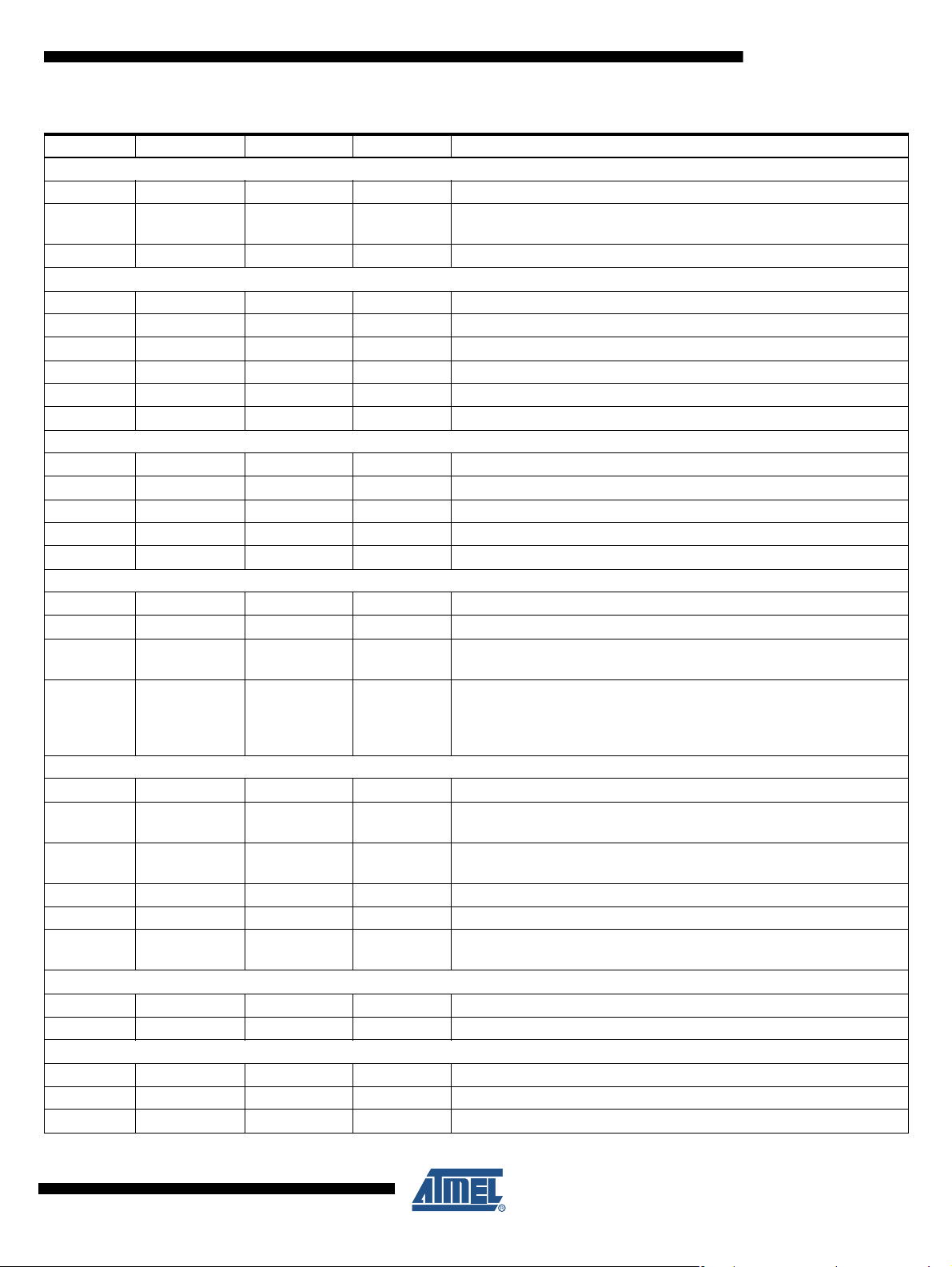
Table 3-2. Signal Description (Continued)
Pin Number Pin Name Type Active Level Pin Description/Comment
Active Antenna Supervision
C8 NANTSHORT DIGITAL IN Low Active antenna short detection Input
G5, G6
F11 ANTON DIGITAL OUT - Active antenna power-on Output
JTAG Interface
E8 DBG_EN DIGITAL IN - Debug enable
F9 TDO DIGITAL OUT - Test data out
G9 TCK DIGITAL IN - Test clock
G10 TMS DIGITAL IN - Test mode select
H10 TDI DIGITAL IN - Test data in
H11 NTRST DIGITAL IN Low Test reset input
Debug/Test
C3 MO ANALOG OUT - IF output buffer
D3 TEST ANALOG IN - Enable IF output buffer
B7 SIGLO DIGITAL OUT - Digital IF (data output “Low”)
B8 SIGHI DIGITAL OUT - Digital IF (data output “High”)
A8 CLK23 DIGITAL OUT - Digital IF (sample clock)
Power Analog Part
C2 VCC1 SUPPLY - Analog supply 3V
E4 VCC2 SUPPLY - Analog supply 3V
G2, G3, H2,
H3
A3, B1, B4,
D2, E[1-3],
F[1-3], G1,
H1
Power Digital Part
A5 VDIG SUPPLY - Digital supply (radio) 1.8V
B9, E5, F12,
G11,H9
A10 VDD_USB SUPPLY -
B5, H5 VDDIO SUPPLY - Variable I/O voltage 1.65V to 3.6V
C5 GDIG SUPPLY - Digital ground (radio)
A6, A9, B11,
F5, H8, H12
LDO18
E11 LDO_IN SUPPLY - 2.3V to 3.6V
E12 LDO_OUT SUPPLY - 1.8V LDO18 output, max. 80 mA
LDOBAT
D11 LDOBAT_IN SUPPLY - 2.3V to 3.6V
D12 VBAT SUPPLY - 1.5V to 3.6V
C12 VBAT18 SUPPLY - 1.8V LDOBAT Output
NAADET0/
NAADET1
VBP SUPPLY - Analog supply 3V
GNDA SUPPLY - Analog Ground
VDD18 SUPPLY - Core voltage 1.8V
GND SUPPLY - Digital ground
DIGITAL IN Low Active antenna detection Input
USB transceiver supply voltage (3.0V to 3.6V (USB enabled) or 0 to
2.0V (USB disabled))
ATR0635P1
4979D–GPS–06/08
11
Page 12

3.3 Setting GPSMODE0 to GPSMODE12
The start-up configuration of this ROM-based system without external non-volatile memory is
defined by the status of the GPSMODE pins after system reset. Alternatively, the system can be
configured through message commands passed through the serial interface after start-up. This
configuration of the ATR0635P1 can be stored in an external non-volatile memory like
EEPROM. Default designates settings used by ROM firmware if GPSMODE configuration is disabled (GPSMODE0 = 0).
Table 3-3. GPSMODE Functions
Pin Function
GPSMODE0 (P1) Enable configuration with GPSMODE pins
GPSMODE1 (P9)
GPSMODE2 (P12)
GPSMODE3 (P13)
GPSMODE4 (P14)
GPSMODE5 (P17)
GPSMODE6 (P19)
GPSMODE7 (P23) USB power mode
GPSMODE8 (P24) General I/O configuration
GPSMODE9 (P25)
GPSMODE10 (P26)
GPSMODE11 (P27)
GPSMODE12 (P29) Serial I/O configuration
This pin (EXTINT0) is used for FixNOW
configuration.
GPS sensitivity settings
This pin (NAADET1) is used as active antenna supervisor input and not used for
GPSMODE configuration. This is the default selection if GPSMODE configuration is
disabled.
Serial I/O configuration
This pin (NAADET0) is used as an active Antenna Supervisor input and not used for
GPSMODE configuration
General I/O configuration
™
functionality and not used for GPSMODE
In the case that GPSMODE pins with internal pull-up or pull-down resistors are connected to
GND/VDD18, additional current is drawn over these resistors. Especially GPSMODE3 can
impact the back-up current.
3.3.1 Enable GPSMODE Pin Configuration
Table 3-4. Enable Configuration With GPSMODE Pins
GPSMODE0
(Reset = PD) Description
(1)
0
1 Use settings as specified with GPSMODE[2, 3, 5 to 8, 10 to 12]
Note: 1. Leave open
Ignore all GPSMODE pins. The default settings as indicated below are used.
If the GPSMODE configuration is enabled (GPSMODE0 = 1) and the other GPSMODE pins are
not connected externally, the reset default values of the internal pull-down and pull-up resistors
will be used.
12
ATR0635P1
4979D–GPS–06/08
Page 13

3.3.2 Sensitivity Settings
Table 3-5. GPS Sensitivity Settings
GPSMODE3
(Fixed PU)
Notes: 1. Increased back-up current
For all GPS receivers the sensitivity depends on the integration time of the GPS signals. Therefore there is a trade-off between sensitivity and the time to detect the GPS signal (Time to first
fix). The three modes, “Fast Acquisition”, “Normal” and “High Sensitivity”, have a fixed integration time. The “Normal” mode, recommended for the most applications, is a trade off between
the sensitivity and TTFF. The “Fast Acquisition” mode is optimized for fast acquisition, at the
cost of a lower sensitivity. The “High Sensitivity” mode is optimized for higher sensitivity, at the
cost of longer TTFF. The “Auto” mode adjusts the integration time (sensitivity) automatically
according to the measured signal levels. That means the receiver with this setting has a fast
TTFF at strong signals, a high sensitivity to acquire weak signals but some times at medium signal level a higher TTFF as the “Normal” mode. These sensitivity settings affect only the startup
performance not the tracking performance.
(1)
0
(1)
0
(2)
1
(2)
1
2. Leave open
GPSMODE2
(Reset = PU) Description
0 Auto mode (Default ROM value)
(2)
1
Fast mode
0 Normal mode
(2)
1
High sensitivity
ATR0635P1
3.4 Serial I/O Configuration
The ATR0635P1 features a two-stage I/O-message and protocol-selection procedure for the two
available serial ports. At the first stage, a certain protocol can be enabled or disabled for a given
USART port or the USB port. Selectable protocols are RTCM, NMEA and UBX. At the second
stage, messages can be enabled or disabled for each enabled protocol on each port. In all configurations described below, all protocols are enabled on all ports, but output messages are
enabled in a way that ports appear to communicate at only one protocol. However, each port will
accept any input message in any of the three implemented protocols
Table 3-6. Serial I/O Configuration
USART1/USB
GPSMODE12
(Reset = PU)
000
GPSMODE6
(Reset = PU)
GPSMODE5
(Reset = PD)
(2)
(Output Protocol/
Baud Rate (kBaud))
UBX/57.6 NMEA/19.2 High User, Notice, Warning, Error
0 0 1 UBX/38.4 NMEA/9.6 Medium User, Notice, Warning, Error
01
01
(2)
1
(2)
1
(2)
1
(2)
1
(2)
(2)
00
0 1 NMEA/4.8 UBX/19.2 Low User, Notice, Warning, Error
(2)
1
(2)
1
(2)
0
UBX/19.2 NMEA/4.8 Low User, Notice, Warning, Error
1 –/Auto –/Auto Off None
(2)
(2)
0
NMEA/19.2 UBX/57.6 High User, Notice, Warning, Error
NMEA/9.6 UBX/38.4 Medium User, Notice, Warning, Error
1 UBX/115.2 NMEA/19.2 Debug All
Notes: 1. See Table 3-7 to Table 3-10 on page 14, the messages are described in the ANTARIS4 protocol specification
2. Leave open
USART2
(Output Protocol/
Baud Rate (kBaud)) Messages
(1)
Information Messages
4979D–GPS–06/08
13
Page 14

Both USART ports accept input messages in all three supported protocols (NMEA, RTCM and
UBX) at the configured baud rate. Input messages of all three protocols can be arbitrarily mixed.
Response to a query input message will always use the same protocol as the query input message. The USB port does only accept NMEA and UBX as input protocol by default. RTCM can
be enabled via protocol messages on demand.
In Auto mode, no output message is sent out by default, but all input messages are accepted at
any supported baud rate. Again, USB is restricted to only NMEA and UBX protocols. Response
to query input commands will be given by the same protocol and baud rate as it was used for the
query command. Using the respective configuration commands, periodic output messages can
be enabled.
The following message settings are used in the tables below:
Table 3-7. Supported Messages at Setting Low
NMEA Port Standard GGA, RMC
UBX Port
NAV SOL, SVINFO
MON EXCEPT
Table 3-8. Supported Messages at Setting Medium
NMEA Port Standard GGA, RMC, GSA, GSV, GLL, VTG, ZDA
UBX Port NAV
SOL, SVINFO, POSECEF, POSLLH, STATUS, DOP, VELECEF,
VELNED, TIMEGPS, TIMEUTC, CLOCK
Table 3-9. Supported Messages at Setting High
NMEA Port
UBX Port
Standard GGA, RMC, GSA, GSV, GLL, VTG, ZDA, GRS, GST
Proprietary PUBX00, PUBX03, PUBX04
NAV
MON SCHD, IO, IPC, EXCEPT
SOL, SVINFO, POSECEF, POSLLH, STATUS, DOP, VELECEF,
VELNED, TIMEGPS, TIMEUTC, CLOCK
Table 3-10. Supported Messages at Setting Debug (Additional Undocumented Message May
be Part of Output Data)
NMEA Port
UBX Port
Standard GGA, RMC, GSA, GSV, GLL, VTG, ZDA, GRS, GST
Proprietary PUBX00, PUBX03, PUBX04
NAV
MON SCHD, IO, IPC, EXCEPT
RXM RAW (RAW message support requires an additional license)
SOL, SVINFO, POSECEF, POSLLH, STATUS, DOP, VELECEF,
VELNED, TIMEGPS, TIMEUTC, CLOCK
14
ATR0635P1
4979D–GPS–06/08
Page 15

The following settings apply if GPSMODE configuration is not enabled, that is, GPSMODE = 0
(ROM defaults):
Table 3-11. Serial I/O Default Setting if GPSMODE Configuration is Deselected
Baud rate (kBaud) 57.6 57.6
Input protocol UBX, NMEA UBX, NMEA, RTCM UBX, NMEA, RTCM
Output protocol NMEA NMEA UBX
Messages GGA, RMC, GSA, GSV GGA, RMC, GSA, GSV
Information
messages (UBX INF
or NMEA TXT)
3.4.1 USB Power Mode
For correct response to the USB host queries, the device has to know its power mode. This is
configured via GPSMODE7. If set to bus powered, an upper current limit of 100 mA is reported
to the USB host; that is, the device classifies itself as a “low-power bus-powered function” with
no more than one USB power unit load.
(GPSMODE0 = 0)
USB
NMEA
User Notice, Warning,
Error
USART1
NMEA
User, Notice, Warning,
Error
ATR0635P1
USART2
UBX
NAV: SOL, SVINFO
MON: EXCEPT
User, Notice, Warning,
Error
Table 3-12. USB Power Modes
GPSMODE7 (Reset = PU) Description
Note: 1. Leave open
3.4.2 Active Antenna Supervisor
The two pins P0/NANTSHORT and P15/ANTON plus one pin of P25/NAADET0/MISO or
P14/NAADET1 are always initialized as general purpose I/Os and used as follows:
• P15/ANTON is an output which can be used to switch on and off antenna power supply.
• Input P0/NANTSHORT will indicate an antenna short circuit, i.e. zero DC voltage at the
antenna, to the firmware. If the antenna is switched off by output P15/ANTON, it is assumed
that also input P0/NANTSHORT will signal zero DC voltage, i.e. switch to its active low state.
• Input P25/NAADET0/MISO or P14/NAADET1 will indicate a DC current into the antenna. In
case of short circuit, both P0 and P25/P14 will be active, i.e. at low level. If the antenna is
switched off by output P15/ANTON, it is assumed that also input P25/NAADET0/MISO will
signal zero DC current, i.e. switch to its active low state. Which pin is used as NAADET (P14
or P25) depends on the settings of GPSMODE11 and GPSMODE10 (see Table 3-14 on
page 16).
0 USB device is bus-powered (maximum current limit 100 mA)
(1)
1
USB device is self-powered (default ROM value)
4979D–GPS–06/08
15
Page 16

Table 3-13. Pin Usage of Active Antenna Supervisor
Pin Usage Meaning
Active antenna short circuit detection
P0/NANTSHORT NANTSHORT
High = No antenna DC short circuit present
Low = Antenna DC short circuit present
P25/NAADET0/
MISO or
P14/NAADET1
NAADET
Active antenna detection input
High = No active antenna present
Low = Active antenna is present
Active antenna power on output
P15/ANTON ANTON
High = Power supply to active antenna is switched on
Low = Power supply to active antenna is switched off
Table 3-14. Antenna Detection I/O Settings
GPSMODE11
(Reset = PU)
0 0 0 P25/NAADET0/MISO
001
01
01
(1)
1
(1)
1
(1)
1
(1)
1
Note: 1. Leave open
GPSMODE10
(Reset = PU)
(1)
(1)
GPSMODE8
(Reset = PU) Location of NAADET Comment
(1)
P25/NAADET0/MISO
0 P14/NAADET1
(1)
1
P14/NAADET1
(Default ROM value)
0 0 P14/NAADET1
01
(1)
1
(1)
1
(1)
P14/NAADET1
0 P25/NAADET0/MISO
(1)
1
P25/NAADET0/MISO
Reserved for further use.
Do not use this setting.
Reserved for further use.
Do not use this setting.
Reserved for further use.
Do not use this setting.
16
The Antenna Supervisor Software will be configured as follows:
1. Enable Control Signal
2. Enable Short Circuit Detection (power down antenna via ANTON if short is detected via
NANTSHORT)
3. Enable Open Circuit Detection via NAADET
The antenna supervisor function may not be disabled by GPSMODE pin selection.
If the antenna supervisor function is not used, please leave open ANTON, NANTSHORT and
NAADET.
ATR0635P1
4979D–GPS–06/08
Page 17

3.4.3 External Connections for a Working GPS System
ATR0635P1
see Table 3-15
see Table 3-15
see Table 3-15
see Table 3-15
see Table 3-15
(see Power Supply)
+3V
USB_DM
USB_DP
P18
Optional
USART 2
Optional
USART 1
Optional
USB
P31
P21
VCC1
VBP
P22
P20
P8
P9
P12 - 17
VBAT
VBAT18
LDO_IN
LDOBAT_IN
P23 - 27
P19
P0 - 2
STATUS LED
TIMEPULSE
see Table 3-15 P29 - 30
NC: Not connected
(see Power Supply)
+3V
GND
+3V
(see Power Supply)
VCC2
+3V
(see Power Supply)
+3V
(see Power Supply)
VDD_USB
VDDIO
VDIG
LDO_OUT
VDD18
LDO_EN
NSHDN
GNDA
GNDD
GND analog
GND digital
AGCO
GND
EGC
TEST
MO
GND analog
NC
NC
SDI
P30/AGCOUT0
NC
NC
NC
NC
NC
NC
NC
TCK
NTRST
TDI
NRESET
TDO
DBG_EN
TMS
PUXTO
NSLEEP
PURF
RF_ON
NC
NC
NC CLK23
SIGHI
SIGLO
XT_IN
XT_OUT
32.768 kHz
(see RTC)
XTO
NXTO
X
NX
SAW
LNA
(optional)
ATR0610
RF
NRF
TCXO
23.104 MHz
(see GPS Crystal)
NC
NC
Figure 3-2. Example of an External Connection (ATR0635P1)
ATR0635P1
4979D–GPS–06/08
17
Page 18

Table 3-15. Recommended Pin Connections
Pin Name Recommended External Circuit
P0/NANTSHORT Internal pull-down resistor; leave open if Antenna Supervision functionality is unused.
Internal pull-down resistor; leave open in order to disable the GPSMODE pin configuration feature. Connect
P1/GPSMODE0
P2/BOOT_MODE Internal pull-down resistor; leave open.
P8/STATUSLED Output in default ROM firmware: leave open if not used
P9/EXTINT0 Internal pull-up resistor; leave open if unused.
P12/GPSMODE2/NPCS2
P13/GPSMODE3/
EXTINT1
P14/NAADET1 Internal pull-down resistor; leave open if Antenna Supervision functionality is unused.
P15/ANTON Internal pull-down resistor; leave open if Antenna Supervision functionality is unused.
P16/NEEPROM Internal pull-up resistor; leave open if no serial EEPROM is connected. Otherwise connect to GND.
P17/GPSMODE5/SCK1
P18/TXD1 Output in default ROM firmware: leave open if serial interface is not used.
P19/GPSMODE6/SIGLO1
P20/TIMEPULSE/SCK2 Output in default ROM firmware: leave open if time pulse feature is not used.
P21/TXD2 Output in default ROM firmware: leave open if serial interface not used.
P22/RXD2 Internal pull-up resistor; leave open if serial interface is not used.
P23/GPSMODE7/SCK
P24/GPSMODE8/MOSI
P25/NAADET0/MISO Internal pull-down resistor; leave open if Antenna Supervision functionality is unused.
P26/GPSMODE10/NSS/
NPCS0
P27/GPSMODE11/NPCS1
P29/GPSMODE12/NPCS3
P30/AGCOUT0 Internal pull-down resistor; leave open.
P31/RXD1 Internal pull-up resistor; leave open if serial interface is not used.
to VDD18 to enable the GPSMODE pin configuration feature. Refer to GPSMODE definitions in “Setting
GPSMODE0 to GPSMODE12” on page 12.
Internal pull-up resistor; can be left open if the GPSMODE feature is not used. Refer to GPSMODE
definitions in “Setting GPSMODE0 to GPSMODE12” on page 12.
Internal pull-up resistor; can be left open if the GPSMODE feature is not used. Refer to GPSMODE
definitions in “Setting GPSMODE0 to GPSMODE12” on page 12.
Internal pull-down resistor; can be left open if the GPSMODE feature is not used. Refer to GPSMODE
definitions in “Setting GPSMODE0 to GPSMODE12” on page 12.
Internal pull-up resistor; can be left open if the GPSMODE feature is not used. Refer to GPSMODE
definitions in “Setting GPSMODE0 to GPSMODE12” on page 12.
Internal pull-up resistor; can be left open if the GPSMODE feature is not used. Refer to GPSMODE
definitions in “Setting GPSMODE0 to GPSMODE12” on page 12.
Internal pull-up resistor; can be left open if the GPSMODE feature is not used. Refer to GPSMODE
definitions in “Setting GPSMODE0 to GPSMODE12” on page 12.
Internal pull-up resistor; can be left open if the GPSMODE feature is not used. Refer to GPSMODE
definitions in “Setting GPSMODE0 to GPSMODE12” on page 12.
Internal pull-up resistor; can be left open if the GPSMODE feature is not used. Refer to GPSMODE
definitions in “Setting GPSMODE0 to GPSMODE12” on page 12.
Internal pull-up resistor; can be left open if the GPSMODE feature is not used. Refer to GPSMODE
definitions in “Setting GPSMODE0 to GPSMODE12” on page 12.
18
ATR0635P1
4979D–GPS–06/08
Page 19

3.5 Connecting an Optional Serial EEPROM
The ATR0635P1 offers the possibility of connecting an external serial EEPROM. The internal
ROM firmware supports storing the configuration of the ATR0635P1 in serial EEPROM. The pin
P16/NEEPROM signals the firmware that a serial EEPROM is connected to the ATR0635P1.
The ATR0635P1’s 32-bit RISC processor accesses the external memory via SPI (serial peripheral interface). For best results, use a 32-Kbit 1.8V serial EEPROM such as Atmel’s
AT25320AY1-1.8. Figure 3-3 shows an example of the serial EEPROM connection.
Figure 3-3. Example of a Serial EEPROM Connection
ATR0635P1
AT25320AY1-1.8
NC: Not connected
SCK
SI
SO
CS_N
HOLD_N
WP_N
+3V
(see Power Supply)
GND
NC
GND
P23/SCK
P24/MOSI
P25/MISO/NAADET0
P29/NPCS3
P16/NEEPROM
P1/GPSMODE0
GND
NSHDN
LDO_EN
LDO_OUT
VDD18
VDDIO
LDO_IN
LDOBAT_IN
ATR0635P1
Note: The GPSMODE pin configuration feature can be disabled, because the configuration can be
stored in the serial EEPROM. VDDIO is the supply voltage for the pins: P23, P24, P25 and P29.
4979D–GPS–06/08
19
Page 20

4. Power Supply
The ATR0635P1 is supplied with six distinct supply voltages:
• The power supplies for the RF part (VCC1, VCC2, VBP) within 2.7V to 3.3V.
• VDIG, the 1.8V supply of the digital pins of the RF part (SIGHI, SIGLO and CLK23). VDIG
should be connected to VDD18.
• VDD18, the nominal 1.8V supply voltage for the core, the I/O pins, the memory interface and
the test pins and all GPIO pins not mentioned in next item.
• VDDIO, the variable supply voltage within 1.8V to 3.6V for the following GPIO pins: P1, P2,
P8, P12, P14, P16, P17, P18, P19, P20, P21, P23, P24, P25, P26, P27 and P29. In input
mode, these pins are 5V input tolerant.
• VDD_USB, the power supply of the USB pins: USB_DM and USB_DP.
• VBAT18 to supply the backup domain: RTC, backup SRAM and the pins NSLEEP, NSHDN,
LDO_EN, VBAT18, P9/EXTIN0, P13/EXTINT1, P22/RXD2 and P31/RXD1 and the 32kHz
oscillator. In input mode, the four GPIO-pins are 5V input tolerant.
20
ATR0635P1
4979D–GPS–06/08
Page 21

ATR0635P1
ATR0635P1 internal
VDDUSB0V or 3V to 3.6V
1.5V to 3.6V
1 µF
(X7R)
ldoout
ldoen
ldoin
LDO18
LDO_IN
1 µF
(X7R)
VDDIO
2.3V to 3.6V
LDO_ENNSHDN
VDD18
LDO_OUT
USB SM and
transceiver
1.8V to 3.3V
variable I/O domain
RTC
backup memory
Core
vbat18
vbat
VDD
ldobat_in
LDOBAT
LDOBAT_IN
VBAT
VBAT18
RF
VCC1
VCC2
VBP
VDIG
2.7V to 3.3V
Figure 4-1. Connecting Example: Separate Power Supplies for RF and Digital Part Using the Internal LDOs
The ATR0635P1 contains a built in low dropout voltage regulator LDO18. This regulator can be
used if the host system does not provide the core voltage VDD18 of 1.8V nominal. In such case,
LDO18 will provide a 1.8V supply voltage from any input voltage VDD between 2.3V and 3.6V.
The LDO_EN input can be used to shut down VDD18 if the system is in standby mode.
If the host system does supply a 1.8V core voltage directly, this voltage has to be connected to
the VDD18 supply pins of the Core. LDO_EN must be connected to GND. LDO_IN can be connected to GND. LDO_OUT must not be connected.
A second built in low dropout voltage regulator LDOBAT provides the supply voltage for the RTC
and backup SRAM from any input voltage VBAT between 1.5V and 3.6V. The backup battery
delivers the supply current if LDOBAT_IN is not powered.
4979D–GPS–06/08
21
Page 22

The RTC section will be initialized properly if VDD18 is supplied first to the ATR0635P1. If VBAT
ATR0635P1 internal
VDDUSB0V or 3V to 3.6V
1.5V to 3.6V
1 µF
(X7R)
ldoout
ldoen
ldoin
LDO18
LDO_IN
1 µF
(X7R)
VDDIO
2.3V to 3.6V
LDO_ENNSHDN
VDD18
LDO_OUT
USB SM and
transceiver
1.8V to 3.3V
variable I/O domain
RTC
backup memory
Core
vbat18
vbat
VDD
ldobat_in
LDOBAT
LDOBAT_IN
VBAT
VBAT18
RF
VCC1
VCC2
VBP
VDIG
2.7V to 3.3V
is applied first, the current consumption of the RTC and backup SRAM is undetermined.
Figure 4-2. Connecting Example: Common Power Supplies for RF and Digital Part Using the Internal LDOs
The USB Transceiver is disabled if VDD_USB < 2.0V. In this case the pins USB_DM and
USB_DP are connected to GND (internal pull-down resistors). The USB Transceiver is enabled
if VDD_USB within 3.0V and 3.6V.
22
ATR0635P1
4979D–GPS–06/08
Page 23

ATR0635P1
ATR0635P1 internal
VDDUSB0V or 3V to 3.6V
1.5V to 3.6V
ldoout
ldoen
ldoin
LDO18
LDO_IN
1 µF
(X7R)
VDDIO
LDO_EN
VDD18
LDO_OUT
USB SM and
transceiver
1.8V to 3.3V
variable I/O domain
RTC
backup memory
Core
vbat18
vbat
VDD
ldobat_in
LDOBAT
LDOBAT_IN
VBAT
VBAT18
RF
VCC1
VCC2
VBP
VDIG
2.7V to 3.3V
2.3V to 3.6V
1 µF
(X7R)
1.65V to 1.95V
Figure 4-3. Connecting Example: Separate Power Supplies for RF and Digital Part Using 1.8V from Host System
4979D–GPS–06/08
23
Page 24

Figure 4-4. Connecting Example: Power Supply from USB Using the Internal LDOs
ATR0635P1 internal
VDDUSB
1.5V to 3.6V
ldoout
ldoen
ldoin
LDO18
LDO_IN
1 µF
(X7R)
VDDIO
LDO_EN
VDD18
LDO_OUT
USB SM and
transceiver
1.8V to 3.3V
variable I/O domain
RTC
backup memory
Core
vbat18
vbat
VDD
ldobat_in
LDOBAT
LDOBAT_IN
VBAT
VBAT18
RF
VCC1
VCC2
VBP
VDIG
1 µF
(X7R)
NSHDN
External LDO
3.0V to 3.3V
USB-VSB 5V
24
ATR0635P1
4979D–GPS–06/08
Page 25

5. Crystals
B2
A2
B3
A1
X
NX
XTO
NXTO
22 pF
4.7 pF
12 pF
TCXO
Do not
connect
B2
A2
B3
A1
X
NX
XTO
NXTO
22 pF
4.7 pF
12 pF
TCXO
Do not
connect
B2
A2
B3
A1
X
NX
XTO
NXTO
Do not
connect
1:1
V
in
5.1 GPS
ATR0635P1
The ATR0635P1 requires a GPS TCXO. The reference frequency is 23.104 MHz. By connecting
an optional RTC crystal, different power modes are available. The reference frequency is 32.768
kHz.
Figure 5-1. Equivalent Application Examples Using a GPS TCXO (See Table 5-1 on page 26)
4979D–GPS–06/08
Figure 5-2. Application Example Using an External Reference Frequency and Balanced
Inputs (See Table 5-2 on page 26)
25
Page 26

Table 5-1. Specification of GPS TCXOs Appropriate for the Application Example Shown in
XT_IN
XT_OUT
RTC
ATR0635 internal
32 kHz
Crystal
Oscillator
32.768 kHz clock
32.768 kHz
50 ppm
CC
C = 2 × C
load
, C
load
can be derived from the crystal datasheet. Maximum value for C is 25 pF.
Figure 5-1 on page 25
Parameter Comment Min Typ Max Units
Frequency Characteristics
Nominal Frequency
Nominal frequency referenced to
25°C
23.104 MHz
Over operating temperature range 0.5 ±ppm
Frequency deviation
Including calibration, temperature,
soldering and ageing effects
8 ±ppm
Temperature range Operating temperature range –40.0 +85.0 °C
Electrical
Output waveform DC coupled clipped sine wave
Output voltage
(peak-to-peak)
Operating range 0.8 1.5 V
Output load capacitance Tolerable load capacitance 10 pF
Table 5-2. Specification of an External Reference Signal for the Application Example Shown
in Figure 5-2 on page 25
Parameter Comment Min Typ Max Units
Signal Characteristics
Nominal Frequency 23.104 MHz
Waveform Sine wave or clipped sine wave
Amplitude Voltage peak-to-peak 0.6 0.9 1.2 V
5.2 RTC Oscillator
Figure 5-3. Crystal Connection
26
ATR0635P1
4979D–GPS–06/08
Page 27

ATR0635P1
6. Absolute Maximum Ratings
Stresses beyond those listed under “Absolute Maximum Ratings” may cause permanent damage to the device. This is a stress rating
only and functional operation of the device at these or any other conditions beyond those indicated in the operational sections of this
specification is not implied. Exposure to absolute maximum rating conditions for extended periods may affect device reliability.
Parameters Pins Symbol Min Max Unit
Operating temperature T
Storage temperature T
Analog supply voltage VCC1, VCC2, VBP V
Digital supply voltage RF VDIG V
DC supply voltage core VDD18 VDD18 –0.3 +1.95 V
DC supply voltage VDDIO
domain
DC supply voltage USB VDD_USB VDD_USB –0.3 +3.6 V
DC supply voltage LDO18 LDO_IN LDO_IN –0.3 +3.6 V
DC supply voltage LDOBAT LDOBAT_IN LDOBAT_IN –0.3 +3.6 V
DC supply voltage VBAT VBAT VBAT –0.3 +3.6 V
Digital input voltage
Digital input voltage USB_DM, USB_DP –0.3 +3.6 V
Digital input voltage
Note: Minimum/maximum limits are at +25°C ambient temperature, unless otherwise specified.
VDDIO VDDIO –0.3 +3.6 V
P0, P15, P30, XT_IN,
TMS, TCK, TDI, NTRST,
DBG_EN, LDO_EN,
NRESET
P1, P2, P8, P9, P12 to
P14, P16 to P27, P29, P31
op
stg
CC
DIG
–40 +85 °C
–55 +125 °C
–0.3 +3.7 V
–0.3 +3.7 V
–0.3 +1.95 V
–0.3 +5.0 V
7. Handling
The ATR0635P1 is an ESD-sensitive device. The current ESD values are to be defined.
Observe proper precautions for handling.
8. Thermal Resistance
Parameters Symbol Value Unit
Junction ambient according to JEDEC51-5 R
thJA
49.5 K/W
4979D–GPS–06/08
27
Page 28

9. Operating Range
Parameters Pins Symbol Min Typ Max Unit
Analog supply voltage RF VCC1, VCC2, VBP V
Digital supply voltage RF VDIG V
CC
DIG
Digital supply voltage core VDD18 VDD18 1.65 1.8 1.95 V
Digital supply voltage VDDIO
(1)
domain
Digital supply voltage USB
(2)
VDDIO VDDIO 1.65 1.8/3.3 3.6 V
VDD_USB VDD_USB 3.0 3.3 3.6 V
DC supply voltage LDO18 LDO_IN LDO_IN 2.3 3.6 V
DC supply voltage LDOBAT LDOBAT_IN LDOBAT_IN 2.3 3.6 V
DC Supply voltage VBAT VBAT VBAT 1.5 3.6 V
Supply voltage difference
(V
Δ=VCC–VDIG
)
V
Δ
Temperature range Temp –40 +85 °C
Input frequency f
Reference frequency GPS XTAL f
Reference frequency RTC f
RF
TCXO
XTC
Notes: 1. VDDIO is the supply voltage for the following GPIO-pins: P1, P2, P8, P12, P14, P16, P17, P18, P19, P20, P21, P23, P24,
P25, P26, P27 and P29
2. Values defined for operating USB Interface. Otherwise VDD_USB may be connected to ground.
2.70 3.30 V
1.65 1.8 1.95 V
≥ 0.80 V
1575.42 MHz
23.104 MHz
32.768 KHz
10. Electrical Characteristics
If no additional information is given in column Test Conditions, the values apply to temperature range from –40°C to +85°C.
No. Parameters Test Conditions Pin Symbol Min Typ Max Unit Type*
1 RF Front-end
1.1 Output frequency f
1.2 Input impedance (balanced) f
1.3 Mixer conversion gain C3 G
1.4 Mixer noise figure (SSB) C3 NF
1.5 Maximum total gain V
1.6 Total noise figure (SSB) NF
= 23.104 MHz C3 f
TXCO
= 1575.42 MHz D1, C1 Z
RF
= 2.2V G
AGCO
IF
11
MIX
MIX
max_tot
tot
2 VGA/AGC
2.1 Minimum gain V
2.2 Maximum gain V
2.3 Control-voltage sensitivity
= 1.0V G
AGCO
= 2.2V G
AGCO
= 2.2V N
V
AGCO
= 1.0V N
V
AGCO
VGA,min
VGA,max
VGA,min
VGA, max
*) Type means: A = 100% tested, B = 100% correlation tested, C = Characterized on samples, D = Design parameter
Notes: 1. The LDO18 is a built in low dropout voltage regulator, which can be used if the host system does not provide the core volt-
age VDD18.
2. The LDOBAT is a built in low dropout voltage regulator, which provides the supply voltage VBAT18 for the RTC, backup
SRAM, P9, P13, P22, P31, NSLEEP and NSHDN. The LDOBAT voltage regulator switches in battery mode if LDOBAT_IN
falls below 1.5V.
3. Supply voltage VBAT18 for backup domain is generated internally by the LDOBAT.
4. If no current is caused by outputs (pad output current as well as current across internal pull-up resistors)
96.764 MHz A
10–j80 Ω C
10 dB C
6dBC
90 dB C
6.8 dB C
0dBC
70 dB C
6.6 dB/V D
150 dB/V D
28
ATR0635P1
4979D–GPS–06/08
Page 29

ATR0635P1
10. Electrical Characteristics (Continued)
If no additional information is given in column Test Conditions, the values apply to temperature range from –40°C to +85°C.
No. Parameters Test Conditions Pin Symbol Min Typ Max Unit Type*
2.4 AGC cut-off frequency C
2.5 AGC cut-off frequency C
3PMSS
3.1 Voltage level power-on
3.2 Voltage level power-off
4LDO18
(1)
4.1 Output voltage LDO_OUT 1.65 1.8 1.95 V A
4.2 Output current LDO_OUT 30 mA A
4.3 Current consumption
4.4 Current consumption
5LDOBAT
5.1 Output voltage
Current consumption
5.2
LDOBAT_IN
(2)
(3)
(4)
5.3 Current consumption VBAT
5.4 Current consumption
6Core
6.1 DC supply voltage VDD18 V
6.2 DC supply voltage VDDIO V
Low-level input voltage
6.3
VDD18 domain
High-level input voltage
6.4
VDD18 domain
Schmitt trigger threshold
6.5
rising
Schmitt trigger threshold
6.6
falling
*) Type means: A = 100% tested, B = 100% correlation tested, C = Characterized on samples, D = Design parameter
Notes: 1. The LDO18 is a built in low dropout voltage regulator, which can be used if the host system does not provide the core volt-
age VDD18.
2. The LDOBAT is a built in low dropout voltage regulator, which provides the supply voltage VBAT18 for the RTC, backup
SRAM, P9, P13, P22, P31, NSLEEP and NSHDN. The LDOBAT voltage regulator switches in battery mode if LDOBAT_IN
falls below 1.5V.
3. Supply voltage VBAT18 for backup domain is generated internally by the LDOBAT.
4. If no current is caused by outputs (pad output current as well as current across internal pull-up resistors)
= open A4 f
ext
= 100 pF A4 f
ext
3dB_AGC
3dB_AGC
F4, G4,
H4
F4, G4,
H4
After startup, no load, at
room temperature
Standby mode
(LDO_EN = 0), at room
temperature
VBAT18 1.65 1.8 1.95 V A
After startup (sleep/backup
mode), at room
temperature
After startup (backup mode
and LDOBAT_IN = 0V), at
room temperature
After startup (normal
mode), at room
temperature
VDD18 = 1.65V to 1.95V V
VDD18 = 1.65V to 1.95V V
VDD18 = 1.65V to 1.95V CLK23 V
VDD18 = 1.65V to 1.95V CLK23 V
V
PU,on
V
PU,off
O,18
O,IO
IL,18
IH,18
th+,CLK23
th-,CLK23
250 kHz D
33 kHz D
1.3 V A
0.5 V A
80 µA A
15µAA
15 µA A
10 µA A
1.5 mA C
0 VDD18 V D
0 VDDIO V D
–0.3
0.7 ×
VDD18
0.3 ×
VDD18
0.3 ×
VDD18
VDD18
+ 0.3
0.7 ×
VDD18
VC
VC
VC
VC
4979D–GPS–06/08
29
Page 30

10. Electrical Characteristics (Continued)
If no additional information is given in column Test Conditions, the values apply to temperature range from –40°C to +85°C.
No. Parameters Test Conditions Pin Symbol Min Typ Max Unit Type*
6.7 Schmitt trigger hysteresis VDD18 = 1.65V to 1.95V CLK23 V
Schmitt trigger threshold
6.8
rising
Schmitt trigger threshold
6.9
falling
Low-level input voltage
6.10
VDDIO domain
High-level input voltage
6.11
VDDIO domain
Low-level input voltage
6.12
VBAT18 domain
High-level input voltage
6.13
VBAT18 domain
VDD18 = 1.65V to 1.95V NRESET V
VDD18 = 1.65V to 1.95V NRESET V
VDDIO = 1.65V to 3.6V V
VDDIO = 1.65V to 3.6V V
VBAT18 = 1.65V to 1.95V
VBAT18 = 1.65V to 1.95V
A11, B10,
C10, D10
A11, B10,
C10, D10
6.14 Low-level input voltage USB VDD_USB = 3.0V to 3.6V C9, D9 V
High-level input voltage
6.15
USB
Low-level output voltage
6.16
VDD18 domain
High-level output voltage
6.17
VDD18 domain
Low-level output voltage
6.18
VDDIO domain
High-level output voltage
6.19
VDDIO domain
Low-level output voltage
6.20
VBAT18 domain
High-level output voltage
6.21
VBAT18 domain
Low-level output voltage
6.22
USB
High-level output voltage
6.23
USB
Input-leakage current
6.24
(standard inputs and I/Os)
VDD_USB = 3.0V to 3.6V
39Ω source resistance +
27Ω external series resistor
= 1.5 mA,
I
OL
VDD18 = 1.65V
IOH = –1.5 mA,
VDD18 = 1.65V
= 1.5 mA,
I
OL
VDDIO = 3.0V
IOH = –1.5 mA,
VDDIO = 3.0V
IOL = 1 mA
= –1 mA
I
OH
= 2.2 mA,
I
OL
VDD_USB = 3.0V to 3.6V,
27Ω external series resistor
= 0.2 mA,
I
OH
VDD_USB = 3.0V to 3.6V,
27Ω external series resistor
VDD18 = 1.95V
= 0V
V
IL
C9, D9 V
P9, P13,
P22, P31
P9, P13,
P22, P31
DP, DM V
DP, DM V
6.25 Input capacitance I
hyst,CLK23
th+,NRESET
th-,NRESET
IL,IO
IH,IO
V
IL,BAT
V
IH,BAT
IL,USB
IH,USB
V
OL,18
V
OH,18
V
OL,IO
V
OH,IO
V
OL,BAT
V
OH,BAT
OL,USB
OH,USB
I
LEAK
CAP
*) Type means: A = 100% tested, B = 100% correlation tested, C = Characterized on samples, D = Design parameter
Notes: 1. The LDO18 is a built in low dropout voltage regulator, which can be used if the host system does not provide the core volt-
age VDD18.
2. The LDOBAT is a built in low dropout voltage regulator, which provides the supply voltage VBAT18 for the RTC, backup
SRAM, P9, P13, P22, P31, NSLEEP and NSHDN. The LDOBAT voltage regulator switches in battery mode if LDOBAT_IN
falls below 1.5V.
3. Supply voltage VBAT18 for backup domain is generated internally by the LDOBAT.
4. If no current is caused by outputs (pad output current as well as current across internal pull-up resistors)
0.2 0.55 V C
0.8 1.3 V C
0.46 0.77 V C
–0.3 +0.41 V C
1.46 5.0 V C
–0.3 +0.41 V C
1.46 5.0 V C
–0.3 +0.8 V C
2.0 4.6 V C
0.4 V A
VDD18
– 0.45
VA
0.4 V A
VDDIO
– 0.5
VA
0.4 V A
1.2 V A
0.3 V A
2.8 V A
–1 +1 µA C
10 pF D
30
ATR0635P1
4979D–GPS–06/08
Page 31

ATR0635P1
10. Electrical Characteristics (Continued)
If no additional information is given in column Test Conditions, the values apply to temperature range from –40°C to +85°C.
No. Parameters Test Conditions Pin Symbol Min Typ Max Unit Type*
Input pull-up resistor
6.26
NRESET
Input pull-up resistors TCK,
6.27
TDI, TMS
Input pull-up resistors P9,
6.28
P13, P22, P31
Input pull-down resistors
6.29
DBG_EN, NTRST
Input pull-down resistors
6.30
P0, P15, P30
Configurable input pull-up
resistors P1, P2, P8, P12,
6.31
P14, P16 to P21, P23 to
VDDIO = 3.6V
= 0V
V
PA D
P27, P29
Configurable input
pull-down resistors P1, P2,
6.32
P8, P12, P14, P16 to P21,
VDDIO = 3.6V
= 3.6V
V
PA D
P23 to P27, P29
Configurable input pull-up
6.33
resistor USB_DP (idle state)
Configurable input pull-up
6.34
resistor USP_DP (operation
state)
Input pull-down resistors
6.35
USB_DP, USB_DM
*) Type means: A = 100% tested, B = 100% correlation tested, C = Characterized on samples, D = Design parameter
Notes: 1. The LDO18 is a built in low dropout voltage regulator, which can be used if the host system does not provide the core volt-
age VDD18.
2. The LDOBAT is a built in low dropout voltage regulator, which provides the supply voltage VBAT18 for the RTC, backup
SRAM, P9, P13, P22, P31, NSLEEP and NSHDN. The LDOBAT voltage regulator switches in battery mode if LDOBAT_IN
falls below 1.5V.
3. Supply voltage VBAT18 for backup domain is generated internally by the LDOBAT.
4. If no current is caused by outputs (pad output current as well as current across internal pull-up resistors)
A7 R
G9, H10,
G10
A11, B10,
C10, D10
E8, H11 R
C8, F11,
G12
C9 R
C9 R
C9, D9 R
PU
R
PU
R
PU
PD
R
PD
R
CPU
R
CPD
CPU
CPU
PD
0.5 1.8 kΩ A
718kΩ A
100 235 kΩ A
718kΩ A
100 235 kΩ A
50 160 kΩ A
40 160 kΩ A
0.9 1.575 kΩ A
1.425 3.09 kΩ A
10 500 kΩ A
4979D–GPS–06/08
31
Page 32

11. Power Consumption
Table 11-1. Leakage Currents
Parameter Conditions Typ. Max. Unit Type*
Leakage current VDD18
Leakage current VDDIO
Leakage current LDOBAT
+ backup domain
*) Type means: A = 100% tested, B = 100% correlation tested, C = Characterized on samples, D = Design
parameter
Table 11-2. Power Consumption
Mode Conditions Typ. Unit Type*
Sleep At 1.8V, no CLK23 0.065
Shutdown RTC, backup SRAM and LDOBAT 0.007 C
Normal
*) Type means: A = 100% tested, B = 100% correlation tested, C = Characterized on samples, D = Design
parameter
VDD18 = 1.95V, no currents
across pull-up resistors,
PLL disabled
VDDIO = 1.95V no currents
across pull-up resistors
No currents across pull-up
resistors
Satellite acquisition 40 C
Normal tracking on 6 channels with 1 fix/s; each
additional active tracking channel adds 0.5 mA
All channels disabled 26 C
10 200 µA A
25µAA
720µAA
mA
29 C
C
32
ATR0635P1
4979D–GPS–06/08
Page 33

ATR0635P1
specifications
according to DIN
technical drawings
Package: BGA96
Dimensions in mm
Top View
Pin A1 Laser Marking
A1 Corner
A1 Corner
C
B
B
0.1C
0.08 C
C
Seating plane
3.
Primary datum and seating plane are defined by the spherical crowns of the solder balls
C
2.
3.
A
A
1234
Bottom View
Issue: 2; 31.05.06
Drawing-No.: 6.580-5005.01-4
nm
n m
5 6 7 8 9 10 11 12 12 11 10 456789321
0.15
0.08
A
B
D
E
F
H
G
C
A
B
D
E
F
H
G
C
0.4
±0.05
10
±0.05
7
±0.05
0.3
±0.05
1.4 max
0.26
±0.04
0.75
±0.05
0.8
0.8
5.6
8.8
1. All dimensions and tolerance conform to ASME Y 14.5M-1994
Note:
5. Unless otherwise specified tolerance: Decimal ±0.05, Angular ±2
˚
5. Raw ball diameter: 0.4 mm ref.
4. The surface finish of the package shall be EDM CHARMILLE #24 - #27
Dimension is measured at the maximum solder ball diameter, parallel to primary datum
C
2.
12. Ordering Information
Extended Type Number Package MPQ Remarks
ATR0635P1-7KQY BGA96 3000
ATR0635-EK1 - 1 Evaluation kit/Road test kit
ATR0635-DK1 - 1
13. Package Information
7mm× 10 mm, 0.8 mm pitch, Pb-free,
RoHS-compliant
Design kit including design guide and PCB
Gerber files
4979D–GPS–06/08
33
Page 34

14. Revision History
Please note that the following page numbers referred to in this section refer to the specific revision
mentioned, not to this document.
Revision No. History
4979D-GPS-06/08
4979C-GPS-07/07
4979B-GPS-03/07 • Table 3-2 “Signal Description” on pages 9 to 11 changed
• Section 8 “Thermal Resistance” on page 27 added
• Section 10 “Electrical Characteristics” numbers 2.6 and 2.7 on page 29
deleted
• Section 10 “Electrical Characteristics” numbers 4.2, 6.7 and 6.26 to 6.35
on pages 29 to 31 changed
• Section 11 “Power Consumption” on page 32 changed
• Table 3-1 “ATR0635P1 Pinout” on page 6 changed
• Section 9 “Electrical Characteristics” numbers 6.31 and 6.32 on page 31
changed
34
ATR0635P1
4979D–GPS–06/08
Page 35

Headquarters International
Atmel Corporation
2325 Orchard Parkway
San Jose, CA 95131
USA
Tel: 1(408) 441-0311
Fax: 1(408) 487-2600
Atmel Asia
Room 1219
Chinachem Golden Plaza
77 Mody Road Tsimshatsui
East Kowloon
Hong Kong
Tel: (852) 2721-9778
Fax: (852) 2722-1369
Product Contact
Web Site
www.atmel.com
Literature Requests
www.atmel.com/literature
Atmel Europe
Le Krebs
8, Rue Jean-Pierre Timbaud
BP 309
78054
Saint-Quentin-en-Yvelines Cedex
France
Tel: (33) 1-30-60-70-00
Fax: (33) 1-30-60-71-11
Technical Support
gps@atmel.com
Atmel Japan
9F, Tonetsu Shinkawa Bldg.
1-24-8 Shinkawa
Chuo-ku, Tokyo 104-0033
Japan
Tel: (81) 3-3523-3551
Fax: (81) 3-3523-7581
Sales Contact
www.atmel.com/contacts
Disclaimer: The information in this document is provided in connection with Atmel products. No license, express or implied, by estoppel or otherwise, to any
intellectual property right is granted by this document or in connection with the sale of Atmel products. EXCEPT AS SET FORTH IN ATMEL’S TERMS AND CONDI-
TIONS OF SALE LOCATED ON ATMEL’S WEB SITE, ATMEL ASSUMES NO LIABILITY WHATSOEVER AND DISCLAIMS ANY EXPRESS, IMPLIED OR STATUTORY
WARRANTY RELATING TO ITS PRODUCTS INCLUDING, BUT NOT LIMITED TO, THE IMPLIED WARRANTY OF MERCHANTABILITY, FITNESS FOR A PARTICULAR
PURPOSE, OR NON-INFRINGEMENT. IN NO EVENT SHALL ATMEL BE LIABLE FOR ANY DIRECT, INDIRECT, CONSEQUENTIAL, PUNITIVE, SPECIAL OR INCIDENTAL DAMAGES (INCLUDING, WITHOUT LIMITATION, DAMAGES FOR LOSS OF PROFITS, BUSINESS INTERRUPTION, OR LOSS OF INFORMATION) ARISING OUT OF
THE USE OR INABILITY TO USE THIS DOCUMENT, EVEN IF ATMEL HAS BEEN ADVISED OF THE POSSIBILITY OF SUCH DAMAGES. Atmel makes no
representations or warranties with respect to the accuracy or completeness of the contents of this document and reserves the right to make changes to specifications
and product descriptions at any time without notice. Atmel does not make any commitment to update the information contained herein. Unless specifically provided
otherwise, Atmel products are not suitable for, and shall not be used in, automotive applications. Atmel’s products are not intended, authorized, or warranted for use
as components in applications intended to support or sustain life.
© 2008 Atmel Corporation. All rights reserved. Atmel®, logo and combinations thereof, and others are registered trademarks or trademarks of
Atmel Corporation or its subsidiaries. ARM
®
, ARMPowered® logo, ARM7TDMI®, Thumb® and others are registered trademarks or trademarks of
Atmel Corporation. Other terms and product names may be trademarks of others.
4979D–GPS–06/08
 Loading...