

Page 1

Features
• 16-channel GPS Correlator
– 8192 Search Bins with GPS Acquisition Accelerator
– Accuracy: 2.5m CEP (2D, Stand Alone)
– Time to First Fix: 34s (Cold Start)
– Acquisition Sensitivity: –140 dBm (With External LNA)
– Tracking Sensitivity: –150 dBm (With External LNA)
• Utilizes the ARM7TDMI
– High-performance 32-bit RISC Architecture
– EmbeddedICE
• 128 Kbytes Internal RAM
• 384 Kbytes Internal ROM with u-blox GPS Firmware
• 1.5-bit ADC On-chip
• Single IF Architecture
• 2 External Interrupts
• 24 User-programmable I/O Lines
• 1 USB Device Port
– Universal Serial Bus (USB) 2.0 Full-speed Device
– Embedded USB V2.0 Full-speed Transceiver
• 2 USARTs
• Master/Slave SPI Interface
– 4 External Slave Chip Selects
• Programmable Watchdog Timer
• Advanced Power Management Controller (APMC)
– Geared Master Clock to Reduce Power Consumption
– Sleep State with Disabled Master Clock
– Hibernate State with 32.768 kHz Master Clock
• Real Time Clock (RTC)
• 1.8V to 3.3V User-definable IO Voltage for Several GPIOs with 5V Tolerance
• 4 KBytes of Battery Backup Memory
• 7 mm × 10 mm 96 Pin BGA Package, 0.8 mm Pitch, Pb-free, RoHS-compliant
®
ARM® Thumb® Processor Core
™
(In-Circuit Emulation)
ANTARIS4
Single-chip GPS
Receiver
ATR0630P1
Automotive
Summary
Benefits
• Fully Integrated Design With Low BOM
• No External Flash Memory Required
• Requires Only a GPS XTAL, No TCXO
• Supports NMEA
• Supports SBAS (WAAS, EGNOS, MSAS)
• Up to 4Hz Update Rate
• Supports A-GPS (Aiding)
• Excellent Noise Performance
®
, UBX Binary and RTCM Protocol for DGPS
NOTE: This is a summary document.
The complete document is available.
For more information, please contact
your local Atmel sales office.
4978AS–GPS–12/07
Page 2

1. Description
The ATR0630P1 is a low-power, single-chip GPS receiver, especially designed to meet the
requirements of mobile applications. It is based on Atmel
grates an RF front-end, filtering, and a baseband processor in a single, tiny 7 mm × 10 mm
96 pin BGA package. Providing excellent RF performance with low noise figure and low power
consumption.
Due to the fully integrated design, just an RF SAW filter, a GPS XTAL (no TCXO) and blocking
capacitors are required to realize a stand-alone GPS functionality.
The ATR0630P1 includes a complete GPS firmware, licensed from u-blox AG, which performs
the GPS operation, including tracking, acquisition, navigation and position data output. For normal PVT (Position/Velocity/Time) applications, there is no need for external Flash- or
ROM-memory.
The firmware supports e.g. the NMEA protocol (2.1 and 2.3), a binary protocol for PVT data,
configuration and debugging, the RTCM protocol for DGPS, SBAS (WAAS, EGNOS and MSAS)
and A-GPS (aiding). It is also possible to store the configuration settings in an optional external
EEPROM.
Due to the integrated ARM7TDMI processor and an intelligent radio architecture, the
ATR0630P1 operates in a complete autonomous mode, utilizing on chip AGC in closed loop
operation.
For maximum performance, we recommend to use the ATR0630P1 together with a low noise
amplifier (e.g. ATR0610).
®
’s ANTARIS®4 technology and inte-
The ATR0630P1 supports assisted GPS.
2
ATR0630P1
4978AS–GPS–12/07
Page 3
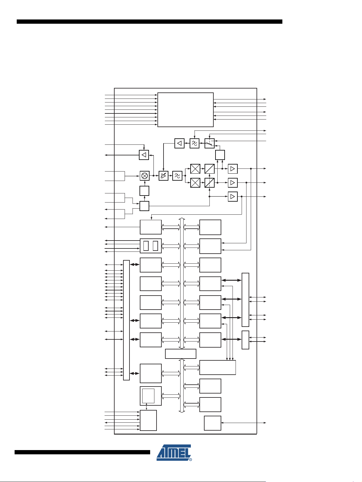
2. Architectural Overview
2.1 Block Diagram
Figure 2-1. ATR0630P1 Block Diagram
PUXTO
PURF
VDD18
VDDIO
VDD_USB
VDIG
VCC1
VCC2
VBP
TEST
Power Supply Manager/
PMSS/Logic
ATR0630P1
VBAT18
VBAT
LDOBAT_IN
LDO_OUT
LDO_IN
LDO_EN
AGCO
EGC
SDI
NRF
XTO
NXTO
RF_ON
NSHDN
NSLEEP
XT_IN
XT_OUT
P20/TIMEPULSE
P29/GPSMODE12
P27/GPSMODE11
P26/GPSMODE10
P24/GPSMODE8
P23/GPSMODE7
P19/GPSMODE6
P17/GPSMODE5
P13/GPSMODE3
P12/GPSMODE2
P1/GPSMODE0
P14/NAADET1
P25/NAADET0
P15/ANTON
P0/NANTSHORT
P9/EXTINT0
P16/NEEPROM
MO
RF
VCO
PLL
PIO2
XTO
Power
Manage-
Advanced
RTC
SMD
PIO2
Special
Interrupt
Advanced
Watchdog
ment
Controller
SRAM
Generator
Controller
Function
Controller
B
RID
E
G
X
NX
A
A
GPS
GPS
Timer
D
D
Accelerator
Correlators
Counter
SPIUSB
USART1 USART2
1
SIGHI
SIGLO
CLK23
P21/TXD2
PIO2
USB
Transceiver
P22/RXD2
P18/TXD1
P31/RXD1
USB_DP
USB_DM
4978AS–GPS–12/07
P8/STATUSLED
P30/AGCOUT0
P2/BOOT_MODE
DBG_EN
NTRST
TDO
TCK
TMS
ROM
SRAM
Reset
PDC2
384K
128K
NRESET
Controller
(EBI)
Memory
Off-Chip
Interface to
ASB APB
ICE
Embedded
ARM7TDMI
TDI
JTAG
3
Page 4

2.2 General Description
The ATR0630P1 has been designed especially for mobile applications. It provides high isolation
between GPS and cellular bands, as well as very low power consumption.
ATR0630P1 is based on the successful ANTARIS4 technology which includes the ANTARIS
ROM software, developed by u-blox AG, Switzerland. ANTARIS provides a proven navigation
engine which is used in high-end car navigation systems, automatic vehicle location (AVL),
security and surveying systems, traffic control, road pricing, and speed camera detectors, and
provides location-based services (LBS) worldwide.
The ANTARIS4 chipset has a very low power consumption and comes with a very low BoM for
the passive components. Especially, due to its fast search engine and GPS accelerator, the
ATR0630P1 only needs a GPS crystal (XTAL) as a resonator for the integrated crystal oscillator
of the ATR0630P1. This saves the considerable higher cost of a TCXO which is required for
competitor’s systems. Also, as the powerful standard software is available in ROM, no external
flash memory is needed.
2.3 PMSS Logic
2.4 XTO
2.5 VCO/PLL
The L1 input signal (f
quency of 1575.42 MHz. The digital modulation scheme is Bi-Phase-Shift-Keying (BPSK) with a
chip rate of 1.023 Mbps.
The power management, startup and shutdown (PMSS) logic ensures reliable operation within
the recommended operating conditions. The external power control signals PUrf and PUxto are
passed through Schmitt trigger inputs to eliminate voltage ripple and prevent undesired behavior
during start-up and shut-down. Digital and analog supply voltages are analyzed by a monitoring
circuit, enabling the startup of the IC only when it is within a safe operating range.
The XTO is designed for minimum phase noise and frequency perturbations. The balanced
topology gives maximum isolation from external and ground coupled noise. The built-in jump
start circuitry ensures reliable start-up behavior of any specified crystal. For use with an external
TCXO, the XTO circuitry can be used as a single-ended or balanced input buffer.
The recommended reference frequency is: f
The frequency synthesizer features a balanced VCO and a fully integrated loop filter, thus no
external components are required. The VCO combines very good phase noise behavior and
excellent spurious suppression. The relation between the reference frequency (f
VCO center frequency (f
) is a Direct Sequence Spread Spectrum (DSSS) signal with a center fre-
RF
= 23.104 MHz.
XTO
) and the
XTO
) is given by: f
VCO
VCO=fXTO
× 64 = 23.104 MHz × 64 = 1478.656 MHz.
2.6 RF Mixer/Image Filter
Combined with the antenna, an external LNA provides a first band-path filtering of the signal.
Atmel’s ATR0610 is recommended for the LNA due to its low noise figure, high linearity and low
power consumption. The output of the LNA drives a SAW filter, which provides image rejection
for the mixer and the required isolation to all GSM bands. The output of the SAW filter is fed into
a highly linear mixer with high conversion gain and excellent noise performance.
4
ATR0630P1
4978AS–GPS–12/07
Page 5

2.7 VGA/AGC
The on-chip automatic gain control (AGC) stage sets the gain of the VGA in order to optimally
load the input of the following analog-to-digital converter. The AGC control loop can be selected
for on-chip closed-loop operation or for baseband controlled gain mode.
2.8 Analog-to-digital Converter
The analog-to-digital converter stage has a total resolution of 1.5 bits. It comprises balanced
comparators and a sub-sampling unit, clocked by the reference frequency (f
spectrum of the digital output signal (f
4.348 MHz.
2.9 Baseband
The GPS baseband core includes a 16-channel correlator and is based on an ARM7TDMI ARM
processor core with very low power consumption. It has a high-performance 32 bit RISC architecture, uses a high-density 16-bit instruction set, The ARM standard In-Circuit Emulation debug
interface is supported via the JTAG/ICE port of the ATR0630P1.
The ATR0630P1 architecture consists of two main buses, the Advanced System Bus (ASB) and
the Advanced Peripheral Bus (APB). The ASB is designed for maximum performance. It interfaces the processor with the on-chip 32-bit memories and the external memories and devices by
means of the External Bus Interface (EBI). The APB is designed for accesses to on-chip peripherals and is optimized for low power consumption. The AMBA
between the ASB and the APB.
ATR0630P1
). The frequency
XTO
), present at the data outputs SIGLO and SIGH1, is
OUT
™
Bridge provides an interface
An on-chip Peripheral Data Controller (PDC2) transfers data between the on-chip USARTs/SPI
and the on- and off-chip memories without processor intervention. Most importantly, the PDC2
removes the processor interrupt handling overhead and significantly reduces the number of
clock cycles required for a data transfer. It can transfer up to 64K contiguous bytes without
reprogramming the starting address. As a result, the performance of the microcontroller is
increased and the power consumption reduced.
All of the external signals of the on-chip peripherals are under the control of the Parallel I/O Controller (PIO2). The PIO2 Controller can be programmed to insert an input filter on each pin or
generate an interrupt on a signal change. After reset, the user must carefully program the PIO2
Controller in order to define which peripheral signals are connected with off-chip logic.
The ATR0630P1 features a Programmable Watchdog Timer.
An Advanced Power Management Controller (APMC) allows for the peripherals to be deactivated individually. Automatic master clock gearing reduces power consumption. A Sleep Mode
is available with disabled 23.104 MHz master clock, as well as a Back-up Mode operating
32.768 kHz master clock.
A 32.768 kHz Real Time Clock (RTC), together with a buit-in battery back-up SRAM, allows for
storage of Almanac, Ephemeris, software configurations to make quick hot- and warm starts.
The ATR0630P1 includes full GPS firmware, licensed from u-blox AG, Switzerland. Features of
the ROM firmware are described in software documentation available from u-blox AG,
Switzerland.
4978AS–GPS–12/07
5
Page 6

3. Pin Configuration
3.1 Pinout
Figure 3-1. Pinning BGA96 (Top View)
123456789101112
A
B
C
D
E
F
G
H
ATR0630P1
Table 3-1. ATR0630P1 Pinout
Pull Resistor
Pin Name BGA 96 Pin Type
AGCO A4 Analog I/O
CLK23 A8 Digital OUT
DBG_EN E8 Digital IN PD
EGC D4 Digital IN
GDIG C5 Supply
GND A6 Supply
GND A9 Supply
GND B11 Supply
GND F5 Supply
GND H8 Supply
GND H12 Supply
GNDA A3 Supply
GNDA B1 Supply
Notes: 1. PD = internal pull-down resistor, PU = internal pull-up resistor, OH = switched to Output High at reset
2. VBAT18 represent the internal power supply of the backup power domain.
3. VDD_USB is the supply voltage for following the USB pins: USB_DM and USB_DP. For operation of the USB interface, supply of 3.0V to 3.6V is required.
4. VDDIO is the supply voltage for the following GPIO pins: P1, P2, P8, P12, P14, P16, P17, P18, P19, P20, P21, P23, P24,
P25, P26, P27 and P29.
(Reset Value)
(1)
Firmware Label
PIO Bank A
IO
6
ATR0630P1
4978AS–GPS–12/07
Page 7

ATR0630P1
Table 3-1. ATR0630P1 Pinout (Continued)
Pull Resistor
Pin Name BGA 96 Pin Type
GNDA B4 Supply
GNDA D2 Supply
GNDA E1 Supply
GNDA E2 Supply
GNDA E3 Supply
GNDA F1 Supply
GNDA F2 Supply
GNDA F3 Supply
GNDA G1 Supply
GNDA H1 Supply
LDOBAT_IN D11 Supply
LDO_EN C11 Digital IN
LDO_IN E11 Supply
LDO_OUT E12 Supply
MO C3 Analog OUT
NRESET A7 Digital I/O Open Drain PU
NRF C1 Analog IN
NSHDN E9 Digital OUT
NSLEEP E10 Digital OUT
NTRST H11 Digital IN PD
NX B2 Analog OUT
NXTO B3 Analog IN
P0 C8 Digital I/O PD NANTSHORT
P1 D8 Digital I/O Configurable (PD) GPSMODE0
P2 C6 Digital I/O Configurable (PD) BOOT_MODE ‘0’
P8 D7 Digital I/O Configurable (PD) STATUSLED ‘0’
P9 A11 Digital I/O PU to VBAT18 EXTINT0 EXTINT0
P12 D6 Digital I/O Configurable (PU) GPSMODE2 NPCS2
P13 B10 Digital I/O PU to VBAT18 GPSMODE3 EXTINT1
P14 G6 Digital I/O Configurable (PD) NAADET1 ‘0’
P15 F11 Digital I/O PD ANTON
P16 G8 Digital I/O Configurable (PU) NEEPROM
P17 H6 Digital I/O Configurable (PD) GPSMODE5 SCK1 SCK1
P18 C7 Digital I/O Configurable (PU) TXD1 TXD1
P19 F6 Digital I/O Configurable (PU) GPSMODE6
Notes: 1. PD = internal pull-down resistor, PU = internal pull-up resistor, OH = switched to Output High at reset
2. VBAT18 represent the internal power supply of the backup power domain.
3. VDD_USB is the supply voltage for following the USB pins: USB_DM and USB_DP. For operation of the USB interface, supply of 3.0V to 3.6V is required.
4. VDDIO is the supply voltage for the following GPIO pins: P1, P2, P8, P12, P14, P16, P17, P18, P19, P20, P21, P23, P24,
P25, P26, P27 and P29.
(Reset Value)
(1)
Firmware Label
PIO Bank A
IO
4978AS–GPS–12/07
7
Page 8

Table 3-1. ATR0630P1 Pinout (Continued)
Pull Resistor
Pin Name BGA 96 Pin Type
P20 G7 Digital I/O Configurable (PD) TIMEPULSE SCK2 SCK2
P21 E6 Digital I/O Configurable (PU) TXD2 TXD2
P22 D10 Digital I/O PU to VBAT18 RXD2 RXD2
P23 F8 Digital I/O Configurable (PU) GPSMODE7 SCK SCK
P24 H7 Digital I/O Configurable (PU) GPSMODE8 MOSI MOSI
P25 G5 Digital I/O Configurable (PD) NAADET0 MISO MISO
P26 B6 Digital I/O Configurable (PU) GPSMODE10 NSS NPCS0
P27 F7 Digital I/O Configurable (PU) GPSMODE11 NPCS1
P28 E7 Digital I/O OH
P29 D5 Digital I/O Configurable (PU) GPSMODE12 NPCS3
P30 G12 Digital I/O PD AGCOUT0 AGCOUT0
P31 C10 Digital I/O PU to VBAT18 RXD1 RXD1
PURF G4 Digital IN
PURF H4 Digital IN
PUXTO F4 Digital IN
RF D1 Analog IN
RF_ON F10 Digital OUT PD
SDI C4 Digital IN
SIGHI0 B8 Digital OUT
SIGLO0 B7 Digital OUT
TCK G9 Digital IN PU
TDI H10 Digital IN PU
TDO F9 Digital OUT
TEST D3 Analog IN
TMS G10 Digital IN PU
USB_DM D9 Digital I/O
USB_DP C9 Digital I/O
VBAT D12 Supply
(2)
VBAT18
VBP G2 Supply
VBP G3 Supply
VBP H2 Supply
VBP H3 Supply
VCC1 C2 Supply
VCC2 E4 Supply
Notes: 1. PD = internal pull-down resistor, PU = internal pull-up resistor, OH = switched to Output High at reset
C12 Supply
2. VBAT18 represent the internal power supply of the backup power domain.
3. VDD_USB is the supply voltage for following the USB pins: USB_DM and USB_DP. For operation of the USB interface, supply of 3.0V to 3.6V is required.
4. VDDIO is the supply voltage for the following GPIO pins: P1, P2, P8, P12, P14, P16, P17, P18, P19, P20, P21, P23, P24,
P25, P26, P27 and P29.
(Reset Value)
(1)
Firmware Label
PIO Bank A
IO
8
ATR0630P1
4978AS–GPS–12/07
Page 9

Table 3-1. ATR0630P1 Pinout (Continued)
Pull Resistor
Pin Name BGA 96 Pin Type
VDD_USB
VDD18 H9 Supply
VDD18 G11 Supply
VDD18 F12 Supply
VDD18 B9 Supply
VDD18 E5 Supply
VDDIO
VDDIO H5 Supply
XT_IN A12 Analog IN
XT_OUT B12 Analog OUT
Notes: 1. PD = internal pull-down resistor, PU = internal pull-up resistor, OH = switched to Output High at reset
(3)
A10 Supply
(4)
VDIG A5 Supply
X A2 Analog OUT
XTO A1 Analog Input
2. VBAT18 represent the internal power supply of the backup power domain.
3. VDD_USB is the supply voltage for following the USB pins: USB_DM and USB_DP. For operation of the USB interface, sup-
4. VDDIO is the supply voltage for the following GPIO pins: P1, P2, P8, P12, P14, P16, P17, P18, P19, P20, P21, P23, P24,
B5 Supply
ply of 3.0V to 3.6V is required.
P25, P26, P27 and P29.
(Reset Value)
(1)
Firmware Label
PIO Bank A
IO
ATR0630P1
3.2 Signal Description
Table 3-2. Signal Description
Pin Number Pin Name Type Active Level Pin Description/Comment
RF Section
D1 RF ANALOG IN - Input from SAW filter
C1 NRF ANALOG IN - Inverted input from SAW filter
GPS XTAL Section
A1 XTO ANALOG IN - XTO input (23.104 MHz)/optional TCXO input
B3 NXTO ANALOG IN - Inverted XTO input (23.104 MHz)/optional TCXO input
A2 X ANALOG OUT - XTO interface (capacitor)
B2 NX ANALOG OUT - Inverted XTO interface (capacitor)
RTC Section
A12 XT_IN ANALOG IN - Oscillator input (32.768 kHz)
B12 XT_OUT ANALOG OUT - Oscillator output (32.768 kHz)
Automatic Gain Control, bandwidth setting
A4 AGCO ANALOG IO - Automatic gain control analog voltage, connect shunt capacitor to GND
D4 EGC DIGITAL IN -
G12 AGCOUT0 DIGITAL OUT - Software gain control
C4 SDI DIGITAL IN - Software gain control
Enable external gain control
(high = software gain control, low = automatic gain control)
4978AS–GPS–12/07
9
Page 10

Table 3-2. Signal Description (Continued)
Pin Number Pin Name Type Active Level Pin Description/Comment
Boot Section
C6 BOOT_MODE DIGITAL IN - Leave open, internal pull down
Reset
A7 NRESET DIGITAL IN Low Reset input; open drain with internal pull-up resistor
APMC/Power Management
E9 NSHDN DIGITAL OUT Low Shutdown output, connect to LDO_EN (C11)
C11 LDO_EN DIGITAL IN - Enable LDO18
E10 NSLEEP DIGITAL OUT Low Power-up output for GPS XTAL, connect to PUXTO (F4)
F4 PUXTO DIGITAL IN - Power-up input for GPS XTAL
G4, H4 PURF DIGITAL IN - Power-up input for GPS radio
F10 RF_ON DIGITAL OUT - Power-up output for GPS radio, connect to PURF (G4, H4)
Advanced Interrupt Controller (AIC)
A11, B10 EXTINT0-1 DIGITAL IN
USART
C10, D10 RXD1/RXD2 DIGITAL IN - USART receive data
C7, E6 TXD1/TXD2 DIGITAL OUT - USART transmit data
H6, G7 SCK1/SCK2 DIGITAL I/O - External synchronous serial clock
USB
C9 USB_DP DIGITAL I/O - USB data (D+)
D9 USB_DM DIGITAL I/O - USB data (D-)
SPI Interface
F8 SCK DIGITAL I/O - SPI clock
H7 MOSI DIGITAL I/O - Master out slave in
G5 MISO DIGITAL I/O - Master in slave out
B6 NSS/NPCS0 DIGITAL I/O Low Slave select
F7, D6, D5
PIO
A11, B[6,10],
C[6-8,10],
D[5-8,10],
E[6,7],
F[6-8],
G[5-8],
H[6,7]
Configuration
B[6,10],
D[5,6,8],
F[6-8], H[6,7]
G8 NEEPROM DIGITAL IN Low Enable EEPROM support
GPS
D7 STATUSLED DIGITAL OUT - Status LED
G7 TIMEPULSE DIGITAL OUT - GPS synchronized time pulse
NPCS1/NPCS2
/NPCS3
P0 to P31 DIGITAL I/O - Programmable I/O ports
GPSMODE0-1
2
DIGITAL OUT Low Slave select
DIGITAL IN - GPS mode pins
High/Low/
Edge
External interrupt request
10
ATR0630P1
4978AS–GPS–12/07
Page 11

Table 3-2. Signal Description (Continued)
Pin Number Pin Name Type Active Level Pin Description/Comment
Active Antenna Supervision
C8 NANTSHORT DIGITAL IN Low Active antenna short detection Input
G5, G6
F11 ANTON DIGITAL OUT - Active antenna power-on Output
JTAG Interface
E8 DBG_EN DIGITAL IN - Debug enable
F9 TDO DIGITAL OUT - Test data out
G9 TCK DIGITAL IN - Test clock
G10 TMS DIGITAL IN - Test mode select
H10 TDI DIGITAL IN - Test data in
H11 NTRST DIGITAL IN Low Test reset input
Debug/Test
C3 MO ANALOG OUT - IF output buffer
D3 TEST ANALOG IN - Enable IF output buffer
B7 SIGLO DIGITAL OUT - Digital IF (data output “Low”)
B8 SIGHI DIGITAL OUT - Digital IF (data output “High”)
A8 CLK23 DIGITAL OUT - Digital IF (sample clock)
Power Analog Part
C2 VCC1 SUPPLY - Analog supply 3V
E4 VCC2 SUPPLY - Analog supply 3V
G2, G3, H2,
H3
A3, B1, B4,
D2, E[1-3],
F[1-3], G1,
H1
Power Digital Part
A5 VDIG SUPPLY - Digital supply (radio) 1.8V
B9, E5, F12,
G11,H9
A10 VDD_USB SUPPLY -
B5, H5 VDDIO SUPPLY - Variable I/O voltage 1.65V to 3.6V
C5 GDIG SUPPLY - Digital ground (radio)
A6, A9, B11,
F5, H8, H12
LDO18
E11 LDO_IN SUPPLY - 2.3V to 3.6V
E12 LDO_OUT SUPPLY - 1.8V LDO18 output, max. 80 mA
LDOBAT
D11 LDOBAT_IN SUPPLY - 2.3V to 3.6V
D12 VBAT SUPPLY - 1.5V to 3.6V
C12 VBAT18 SUPPLY - 1.8V LDOBAT Output
NAADET0/
NAADET1
VBP SUPPLY - Analog supply 3V
GNDA SUPPLY - Analog Ground
VDD18 SUPPLY - Core voltage 1.8V
GND SUPPLY - Digital ground
DIGITAL IN Low Active antenna detection Input
USB transceiver supply voltage (3.0V to 3.6V (USB enabled) or 0 to
2.0V (USB disabled))
ATR0630P1
4978AS–GPS–12/07
11
Page 12

3.3 External Connections for a Working GPS System
Figure 3-2. Example of an External Connection (ATR0630P1)
ATR0630P1
LNA
(optional)
ATR0610
NC
SAW
see Table 3-15
see Table 3-15
see Table 3-15
see Table 3-15
see Table 3-15
see Table 3-15 P29 - 30
GND analog
NC
NC CLK23
NC
NC
NC
NC
NC
NC
NC
NC
NC
SIGHI
SIGLO
RF
NRF
RF_ON
PURF
NSLEEP
PUXTO
NRESET
TMS
TCK
TDI
NTRST
TDO
DBG_EN
P0 - 2
P9
P12 - 17
P19
P23 - 27
P30/AGCOUT0
SDI
MO
TEST
EGC
XT_IN
XT_OUT
XTO
NXTO
NX
P8
P20
USB_DM
USB_DP
P31
P18
P22
P21
32.768 kHz
(see RTC)
X
23.104 MHz
(see GPS crystal)
STATUS LED
TIMEPULSE
Optional
USB
Optional
USART 1
Optional
USART 2
+3V
(see Power Supply)
12
GND
(see Power Supply)
GND
NC: Not connected
ATR0630P1
GND digital
GND analog
+3V
AGCO
GNDD
GNDA
NSHDN
LDO_EN
LDO_OUT
VDD18
VDIG
LDO_IN
LDOBAT_IN
VBAT18
VBAT
VDDIO
VDD_USB
VCC1
VCC2
VBP
+3V
(see Power Supply)
+3V
(see Power Supply)
+3V
(see Power Supply)
4978AS–GPS–12/07
Page 13

ATR0630P1
4. Ordering Information
Extended Type Number Package MPQ Remarks
ATR0630P1-7KQY BGA96 3000
ATR0630-EK1 - 1 Evaluation kit/Road test kit
ATR0630-DK1 - 1
5. Package Information
7mm× 10 mm, 0.8 mm pitch, Pb-free,
RoHS-compliant
Design kit including design guide and PCB
Gerber files
Package: BGA96
Dimensions in mm
A1 Corner
1234
A
B
C
D
E
F
G
H
5 6 7 8 9 10 1112 12 11 10 456789321
Pin A1 Laser Marking
technical drawings
according to DIN
specifications
Top View
7±0.05
A
B
5.6
0.08
nm
0.15
n m
0.8
0.08 C
C
B
A
Bottom View
8.8
10±0.05
0.4±0.05
0.1C
2.
A1 Corner
A
B
C
D
E
F
G
H
0.8
0.75±0.05
4978AS–GPS–12/07
Drawing-No.: 6.580-5005.01-4
Issue: 2; 31.05.06
Seating plane
0.3±0.05
1.4 max
Note:
1. All dimensions and tolerance conform to ASME Y 14.5M-1994
Dimension is measured at the maximum solder ball diameter, parallel to primary datum
2.
Primary datum and seating plane are defined by the spherical crowns of the solder balls
3.
4. The surface finish of the package shall be EDM CHARMILLE #24 - #27
5. Unless otherwise specified tolerance: Decimal ±0.05, Angular ±2
5. Raw ball diameter: 0.4 mm ref.
C
3.
˚
C
±0.04
0.26
C
13
Page 14

Headquarters International
Atmel Corporation
2325 Orchard Parkway
San Jose, CA 95131
USA
Tel: 1(408) 441-0311
Fax: 1(408) 487-2600
Atmel Asia
Room 1219
Chinachem Golden Plaza
77 Mody Road Tsimshatsui
East Kowloon
Hong Kong
Tel: (852) 2721-9778
Fax: (852) 2722-1369
Product Contact
Web Site
www.atmel.com
Literature Requests
www.atmel.com/literature
Atmel Europe
Le Krebs
8, Rue Jean-Pierre Timbaud
BP 309
78054
Saint-Quentin-en-Yvelines Cedex
France
Tel: (33) 1-30-60-70-00
Fax: (33) 1-30-60-71-11
Technical Support
gps@atmel.com
Atmel Japan
9F, Tonetsu Shinkawa Bldg.
1-24-8 Shinkawa
Chuo-ku, Tokyo 104-0033
Japan
Tel: (81) 3-3523-3551
Fax: (81) 3-3523-7581
Sales Contact
www.atmel.com/contacts
Disclaimer: The information in this document is provided in connection with Atmel products. No license, express or implied, by estoppel or otherwise, to any
intellectual property right is granted by this document or in connection with the sale of Atmel products. EXCEPT AS SET FORTH IN ATMEL’S TERMS AND CONDI-
TIONS OF SALE LOCATED ON ATMEL’S WEB SITE, ATMEL ASSUMES NO LIABILITY WHATSOEVER AND DISCLAIMS ANY EXPRESS, IMPLIED OR STATUTORY
WARRANTY RELATING TO ITS PRODUCTS INCLUDING, BUT NOT LIMITED TO, THE IMPLIED WARRANTY OF MERCHANTABILITY, FITNESS FOR A PARTICULAR
PURPOSE, OR NON-INFRINGEMENT. IN NO EVENT SHALL ATMEL BE LIABLE FOR ANY DIRECT, INDIRECT, CONSEQUENTIAL, PUNITIVE, SPECIAL OR INCIDENTAL DAMAGES (INCLUDING, WITHOUT LIMITATION, DAMAGES FOR LOSS OF PROFITS, BUSINESS INTERRUPTION, OR LOSS OF INFORMATION) ARISING OUT OF
THE USE OR INABILITY TO USE THIS DOCUMENT, EVEN IF ATMEL HAS BEEN ADVISED OF THE POSSIBILITY OF SUCH DAMAGES. Atmel makes no
representations or warranties with respect to the accuracy or completeness of the contents of this document and reserves the right to make changes to specifications
and product descriptions at any time without notice. Atmel does not make any commitment to update the information contained herein. Unless specifically provided
otherwise, Atmel products are not suitable for, and shall not be used in, automotive applications. Atmel’s products are not intended, authorized, or warranted for use
as components in applications intended to support or sustain life.
© 2007, Atmel Corporation. All rights reserved. Atmel®, logo and combinations thereof, and others are registered trademarks or trademarks
of Atmel Corporation or its subsidiaries. ARM
Ltd. Other terms and product names may be trademarks of others.
®
, ARM Powered® logo, Thumb® and others are the registered trademarks or trademarks of ARM
4978AS–GPS–12/07
 Loading...