

Page 1

Features
•
16-channel GPS Correlator
– 8192 Search Bins with GPS Acquisition Accelerator
– Accuracy: 2.5m CEP (Stand-Alone, S/A off)
– Time to First Fix: 34s (Cold Start)
– Acquisition Sensitivity: –140 dBm
– Tracking Sensitivity: –150 dBm
•
Utilizes the ARM7TDMI® ARM® Thumb® Processor Core
– High-performance 32-bit RISC Architecture
– High-density 16-bit Instruction Set
– Embedded ICE (In-circuit Emulator)
•
128 Kbyte Internal RAM
•
384 Kbyte Internal ROM with u-blox GPS Firmware
•
6-channel Peripheral Data Controller (PDC)
•
8-level Priority, Individually Maskable, Vectored Interrupt Controller
– 2 External Interrupts
•
24 User-programmable I/O Lines
•
1 USB Device Port
– Universal Serial Bus (USB) V2.0 Full-speed Device
– Embedded USB V2.0 Full-speed Transceiver
– Suspend/Resume Logic
– Ping-pong Mode for Isochronous and Bulk Endpoints
•
2 USARTs
– 2 Dedicated Peripheral Data Controller (PDC) Channels per USART
•
Master/Slave SPI Interface
– 2 Dedicated Peripheral Data Controller (PDC) Channels
– 8-bit to 16-bit Programmable Data Length
– 4 External Slave Chip Selects
•
Programmable Watchdog Timer
•
Advanced Power Management Controller (APMC)
– Peripherals Can Be Deactivated Individually
– Geared Master Clock to Reduce Power Consumption
– Sleep State with Disabled Master Clock
– Hibernate State with 32.768 kHz Master Clock
•
Real Time Clock (RTC)
•
2.3V to 3.6V or 1.8V Core Supply Voltage
•
Includes Power Supervisor
•
1.8V to 3.3V User-definable I/O Voltage for Several GPIOs with 5V Tolerance
•
4 Kbytes Battery Backup Memory
•
8 mm × 8 mm 56 Pin QFN56 Package
•
Pb-free, RoHS-compliant, Green
GPS Baseband
Processor
ATR0622
Summary
Preliminary
Rev. 4891CS–GPS–01/06
Page 2

1. Description
The GPS baseband processor ATR0622 includes a 16-channel GPS correlator and is based
on the ARM7TDMI
This processor has a high-performance 32-bit RISC architecture and very low power consumption. In addition, a large number of internally banked registers result in very fast
exception handling, making the device ideal for real-time control applications. The ATR0622
has two USART and an USB device port. This port is compliant with the Universal Serial Bus
(USB) V2.0 full-speed device specification.
The ATR0622 includes full GPS firmware, licensed from u-blox AG, which performs the basic
GPS operation, including tracking, acquisition, navigation and position data output. For normal
PVT (Position/Velocity/Time) applications, there is no need for off-chip Flash memory or ROM.
The firmware supports the possibility to store the configuration settings in an optional external
EEPROM. For customer-specific applications, a Software Development Kit is available.
The ATR0622 is manufactured using Atmel’s high-density CMOS technology. By combining
the ARM7TDMI microcontroller core with on-chip SRAM, 16-channel GPS correlator, and a
wide range of peripheral functions on a monolithic chip, the ATR0622 provides a highly flexible
and cost-effective solution for GPS applications.
®
processor core.
2
ATR0622 [Preliminary]
4891CS–GPS–01/06
Page 3
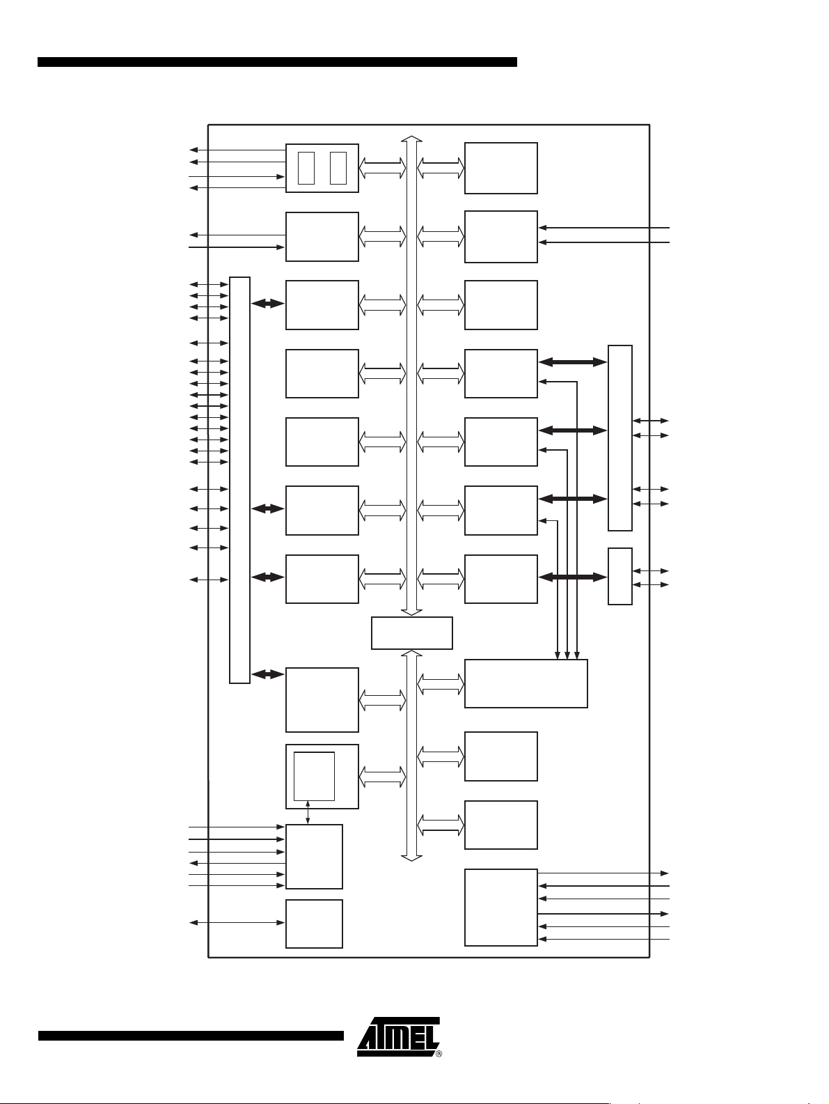
Figure 1-1. ATR0622 Block Diagram
NSHDN
NSLEEP
XT_IN
XT_OUT
RTC
SRAM
ATR0622 [Preliminary]
GPS
Accelerator
RF_ON
CLK23
P15/ANTON
P0/NANTSHORT
P14/NAADET1
P25/NAADET0
P20/TIMEPULSE
P29/GPSMODE12
P27/GPSMODE11
P26/GPSMODE10
P24/GPSMODE8
P23/GPSMODE7
P19/GPSMODE6
P17/GPSMODE5
P13/GPSMODE3
P12/GPSMODE2
P1/GPSMODE0
P9/EXTINT0
P2/BOOT_MODE
P30/AGCOUT0
P8/STATUSLED
P16/NEEPROM
PIO2
Power
Manage-
Advanced
SMD
Generator
PIO2
Controller
Special
Function
Interrupt
Advanced
Watchdog
ment
Controller
Controller
GPS
Correlators
Timer
Counter
SPIUSB
USART1 USART2
PIO2
USB
Transceiver
SIGLO0
SIGHI0
P21/TXD2
P22/RXD2
P18/TXD1
P31/RXD1
USB_DP
USB_DM
DBG_EN
NTRST
TDI
TDO
TCK
TMS
NRESET
(EBI)
Memory
Off-Chip
Interface to
ICE
Embedded
JTAG
Reset
Controller
B
ARM7TDMI
RID
ASB APB
E
G
PDC2
ROM
384K
128K
SRAM
VBAT18
VBAT
LDOBAT_IN
Power
Supply
Manager
LDO_OUT
LDO_IN
LDO_EN
4891CS–GPS–01/06
3
Page 4

2. Architectural Overview
2.1 Description
The ATR0622 architecture consists of two main buses, the Advanced System Bus (ASB) and
the Advanced Peripheral Bus (APB). The ASB is designed for maximum performance. It interfaces the processor with the on-chip 32-bit memories. The APB is designed for accesses to
on-chip peripherals and is optimized for low power consumption. The AMBA
an interface between the ASB and the APB.
An on-chip Peripheral Data Controller (PDC2) transfers data between the on-chip
USARTs/SPI and the on-chip and off-chip memories without processor intervention. Most
importantly, the PDC2 removes the processor interrupt handling overhead and significantly
reduces the number of clock cycles required for a data transfer. It can transfer up to 64K contiguous bytes without reprogramming the starting address. As a result, the performance of the
microcontroller is increased and the power consumption reduced.
The ATR0622 peripherals are designed to be easily programmable with a minimum number of
instructions. Each peripheral has a 16 Kbyte address space allocated in the upper 3 Mbyte of
the 4 Gbyte address space. (Except for the interrupt controller, which has 4 Kbyte address
space.) The peripheral base address is the lowest address of its memory space. The peripheral register set is composed of control, mode, data, status, and interrupt registers.
To maximize the efficiency of bit manipulation, frequently written registers are mapped into
three memory locations. The first address is used to set the individual register bits, the second
resets the bits, and the third address reads the value stored in the register. A bit can be set or
reset by writing a “1” to the corresponding position at the appropriate address. Writing a “0”
has no effect. Individual bits can thus be modified without having to use costly read-modifywrite and complex bit-manipulation instructions.
™
Bridge provides
All of the external signals of the on-chip peripherals are under the control of the Parallel I/O
(PIO2) Controller. The PIO2 Controller can be programmed to insert an input filter on each pin
or generate an interrupt on a signal change. After reset, the user must carefully program the
PIO2 Controller in order to define which peripheral signals are connected with off-chip logic.
The ARM7TDMI
The processor's internal architecture and the ARM
described in the ARM7TDMI datasheet. The memory map and the on-chip peripherals are
described in detail in the ATR0622 full datasheet. The electrical and mechanical characteristics are also documented in the ATR0622 full datasheet.
The ARM standard In-Circuit Emulator (ICE) debug interface is supported via the JTAG/ICE
port of the ATR0622.
For features of the ROM firmware, refer to the software documentation available from u-blox
AG, Switzerland.
®
processor operates in little-endian mode on the ATR0622 GPS Baseband.
®
and Thumb® instruction sets are
4
ATR0622 [Preliminary]
4891CS–GPS–01/06
Page 5
ATR0622 [Preliminary]
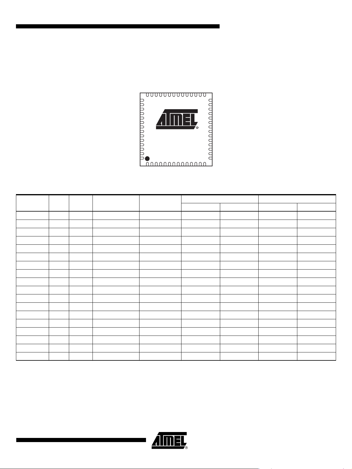
3. Pin Configuration
3.1 Pinout
Figure 3-1. Pinout QFN56 (Top View)
42 29
43 28
ATR0622
56 15
114
Table 3-1. ATR0622 Pinout
Pin
Pin Name QFN56
CLK23 37 IN
DBG_EN 8 IN PD
GND
LDOBAT_IN 21 IN
LDO_EN 25 IN
LDO_IN 20 IN
LDO_OUT 19 OUT
NRESET 41 I/O Open Drain PU
NSHDN 26 OUT
NSLEEP 24 OUT
NTRST 13 IN PD
P0 40 I/O PD NANTSHORT
P1 47 I/O Configurable (PD) GPSMODE0 AGCOUT1
P2 46 I/O Configurable (PD) BOOT_MODE “0”
P8 48 I/O Configurable (PD) STATUSLED “0”
P9 29 I/O PU EXTINT0 EXTINT0
P12 49 I/O Configurable (PU) GPSMODE2 NPCS2
P13 32 I/O PU GPSMODE3 EXTINT1
Notes: 1. PD = internal pull-down resistor, PU = internal pull-up resistor, OH = switched to Output High at reset
2. Ground plane
3. VBAT18 represent the internal power supply of the backup power domain, see section “Power Supply” on page 17.
4. VDDIO is the supply voltage for the following GPIO-pins: P1, P2, P8, P12, P14, P16, P17, P18, P19, P20, P21, P23, P24,
5. VDD_USB is the supply voltage for following the USB-pins: USB_DM and USB_DP, see section “Power Supply” on page
6. This pin is not connected
(2)
P25, P26, P27 and P29, see section “Power Supply” on page 17.
17. For operation of the USB interface, supply of 3.0V to 3.6V is required.
Type
IN
Pull Resistor
(Reset Value)
(1)
Firmware Label
PIO Bank A PIO Bank B
IOIO
4891CS–GPS–01/06
5
Page 6

Table 3-1. ATR0622 Pinout (Continued)
PIO Bank A PIO Bank B
IOIO
Pin Name QFN56
Pin
Type
Pull Resistor
(Reset Value)
(1)
Firmware Label
P14 1 I/O Configurable (PD) NAADET1 “0”
P15 17 I/O PD ANTON
P16 6 I/O Configurable (PU) NEEPROM SIGHI1 NWD_OVF
P17 2 I/O Configurable (PD) GPSMODE5 SCK1 SCK1
P18 45 I/O Configurable (PU) TXD1 TXD1 “0”
P19 53 I/O Configurable (PU) GPSMODE6 SIGLO1 “0”
P20 4 I/O Configurable (PD) TIMEPULSE SCK2 SCK2 TIMEPULSE
P21 52 I/O Configurable (PU) TXD2 TXD2 “0”
P22 30 I/O PU RXD2 RXD2
P23 3 I/O Configurable (PU) GPSMODE7 SCK SCK MCLK_OUT
P24 5 I/O Configurable (PU) GPSMODE8 MOSI MOSI “0”
P25 55 I/O Configurable (PD) NAADET0 MISO MISO “0”
P26 44 I/O Configurable (PU) GPSMODE10 NSS NPCS0 “0”
P27 54 I/O Configurable (PU) GPSMODE11 NPCS1
P29 50 I/O Configurable (PU) GPSMODE12 NPCS3
P30 16 I/O PD AGCOUT0 AGCOUT0 “0”
P31 31 I/O PU RXD1 RXD1
RF_ON 15 OUT PD
SIGHI0 38 IN
SIGLO0 39 IN
TCK 9 IN PU
TDI 10 IN PU
TDO 11 OUT
TMS 12 IN PU
USB_DM 34 I/O
USB_DP 35 I/O
VBAT 22 IN
VBAT18
(3)
23 OUT
VDD18 7, 14 IN
VDD18 18, 36 IN
VDD18 51 IN
(4)
VDDIO
VDD_USB
43, 56 IN
(5)
33 IN
XT_IN 28 IN
XT_OUT 27 OUT
(6)
NC
42
Notes: 1. PD = internal pull-down resistor, PU = internal pull-up resistor, OH = switched to Output High at reset
2. Ground plane
3. VBAT18 represent the internal power supply of the backup power domain, see section “Power Supply” on page 17.
4. VDDIO is the supply voltage for the following GPIO-pins: P1, P2, P8, P12, P14, P16, P17, P18, P19, P20, P21, P23, P24,
P25, P26, P27 and P29, see section “Power Supply” on page 17.
5. VDD_USB is the supply voltage for following the USB-pins: USB_DM and USB_DP, see section “Power Supply” on page
17. For operation of the USB interface, supply of 3.0V to 3.6V is required.
6. This pin is not connected
6
ATR0622 [Preliminary]
4891CS–GPS–01/06
Page 7

ATR0622 [Preliminary]
3.2 Signal Description
Table 3-2. ATR0622 Signal Description
Module Name Function Type Active Level Comment
EBI BOOT_MODE Boot Mode Input Input –
TXD1 to TXD2 Transmit Data Output Output – PIO-controlled after reset
USART
USB
APMC RF_ON Output – Interface to ATR0601
AIC EXTINT0-1 External Interrupt Request Input
AGC AGCOUT0-1 Automatic Gain Control Output –
RTC
SPI
WD NWD_OVF Watchdog Timer Overflow Output – PIO-controlled after reset
PIO P0 to P31 Programmable I/O Port I/O – Input after reset
GPS
CONFIG
Note: 1. The USB transceiver is disabled if VDD_USB < 2.0V. In this case the pins USB_DM and USB_DP are connected to GND
RXD1 to RXD2 Receive Data Input Input – PIO-controlled after reset
SCK1 to SCK2 External Synchronous Serial Clock I/O – PIO-controlled after reset
USB_DP USB Data (D+) I/O –
USB_DM USB Data (D-) I/O –
High/
Low/
Edge
NSLEEP Sleep Output Output Low Interface to ATR0601
NSHDN Shutdown Output Output Low Connect to pin LDO_EN
XT_IN Oscillator Input Input – RTC oscillator
XT_OUT Oscillator Output Output – RTC oscillator
SCK SPI Clock I/O – PIO-controlled after reset
MOSI Master Out Slave In I/O – PIO-controlled after reset
MISO Master In Slave Out I/O – PIO-controlled after reset
NSS/NPCS0 Slave Select I/O Low PIO-controlled after reset
NPCS1 to NPCS3 Slave Select Output Low PIO-controlled after reset
SIGHI0 Digital IF Input – Interface to ATR0601
SIGLO0 Digital IF Input – Interface to ATR0601
SIGHI1 Digital IF Input – PIO-controlled after reset
SIGLO1 Digital IF Input – PIO-controlled after reset
TIMEPULSE GPS synchronized time pulse Output – PIO-controlled after reset
GPSMODE0-12 GPS Mode Input – PIO-controlled after reset
STATUSLED Status LED Output – PIO-controlled after reset
NEEPROM Enable EEPROM Support Input Low PIO-controlled after reset
ANTON Active antenna power on Output Output – PIO-controlled after reset
NANTSHORT
NAADET0-1 Active antenna detection Input Input Low PIO-controlled after reset
(internal pull-down resistors). The USB transceiver is enabled if VDD_USB is within 3.0V and 3.6V.
Active antenna short circuit
detection Input
Input Low PIO-controlled after reset
PIO-controlled after reset,
internal pull-down resistor
PIO-controlled after reset
Interface to ATR0601
PIO-controlled after reset
4891CS–GPS–01/06
7
Page 8

Table 3-2. ATR0622 Signal Description (Continued)
Module Name Function Type Active Level Comment
TMS Test Mode Select Input – Internal pull-up resistor
TDI Test Data In Input – Internal pull-up resistor
JTAG/ICE
CLOCK
RESET NRESET Reset Input I/O Low
POWER
LDOBAT
LDO18
Note: 1. The USB transceiver is disabled if VDD_USB < 2.0V. In this case the pins USB_DM and USB_DP are connected to GND
(internal pull-down resistors). The USB transceiver is enabled if VDD_USB is within 3.0V and 3.6V.
TDO Test Data Out Output –
TCK Test Clock Input – Internal pull-up resistor
NTRST Test Reset Input Input Low Internal pull-down resistor
DBG_EN Debug Enable Input High Internal pull-down resistor
CLK23 Clock Input Input –
MCLK_OUT Master Clock Output Output – PIO-controlled after reset
VDD18 Power – Core voltage 1.8V
VDDIO Power – Variable IO voltage 1.65V to 3.6V
VDD_USB Power –
GND Power – Ground
LDOBAT_IN Power – 2.3V to 3.6V
VBAT Power – 1.5V to 3.6V
VBAT18 Out – 1.8V backup voltage
LDO_IN LDO In Power – 2.3V to 3.6V
LDO_OUT LDO Out Power – 1.8V core voltage, max. 80 mA
LDO_EN LDO Enable Input –
Interface to ATR0601,
Schmitt trigger input
Open drain with internal pull-up
resistor
USB voltage 0 to 2.0V or
3.0V to 3.6V
(1)
8
ATR0622 [Preliminary]
4891CS–GPS–01/06
Page 9

3.3 Setting GPSMODE0 to GPSMODE12
The start-up configuration of a ROM-based system without external non-volatile memory is
defined by the status of the GPSMODE pins after system reset. Alternatively, the system can
be configured through message commands passed through the serial interface after start-up.
This configuration of the ATR0622 can be stored in an external non-volatile memory like
EEPROM. Default designates settings used by ROM firmware if GPSMODE configuration is
disabled (GPSMODE0 = 0).
Table 3-3. GPSMODE Functions
Pin Function
GPSMODE0 (P1) Enable configuration with GPSMODE pins
GPSMODE1 (P9)
GPSMODE2 (P12)
GPSMODE3 (P13)
GPSMODE4 (P14)
GPSMODE5 (P17)
GPSMODE6 (P19)
GPSMODE7 (P23) USB Power Mode
GPSMODE8 (P24) General I/O Configuration
GPSMODE9 (P25)
GPSMODE10 (P26)
GPSMODE11 (P27)
GPSMODE12 (P29) Serial I/O configuration
This pin (EXTINT0) is used for FixNow functionality and not used for GPSMODE
configuration.
GPS sensitivity settings
This pin (NAADET1) is used as active antenna supervisor input and not used for
GPSMODE configuration. This is the default selection if GPSMODE configuration
is disabled.
Serial I/O configuration
This pin (NAADET0) is used as active antenna supervisor input and not used for
GPSMODE configuration.
General I/O Configuration
ATR0622 [Preliminary]
3.3.1 Enable GPSMODE Pin Configuration
Table 3-4. Enable Configuration with GPSMODE Pins
GPSMODE0
(Reset = PD) Description
0 Ignore all GPSMODE pins. The default settings as indicated below are used.
1 Use settings as specified with GPSMODE[2, 3, 5 to 8, 10 to 12]
If the GPSMODE configuration is enabled (GPSMODE0 = 1) and the other GPSMODE pins
are not connected externally, the reset default values of the internal pull-down and pull-up
resistors will be used.
4891CS–GPS–01/06
9
Page 10

3.3.2 Sensitivity Settings
Table 3-5. GPS Sensitivity Settings
GPSMODE3
(Fixed PU)
0 0 Auto mode
0 1 Fast mode
1 0 Normal mode (Default ROM value)
1 1 High sensitivity
3.3.3 Serial I/O Configuration
The ATR0622 features a two-stage I/O message and protocol selection procedure for the two
available serial ports. At the first stage, a certain protocol can be enabled or disabled for a
given USART port or the USB port. Selectable protocols are RTCM, NMEA and UBX. At the
second stage, messages can be enabled or disabled for each enabled protocol on each port.
In all configurations discussed below, all protocols are enabled on all ports. But output messages are enabled in a way that ports appear to communicate at only one protocol. However,
each port will accept any input message in any of the three implemented protocols
Table 3-6. Serial I/O Configuration
GPSMODE12
(Reset = PU)
0 0 0 UBX/57.6 NMEA/19.2 High User, Notice, Warning, Error
0 0 1 UBX/38.4 NMEA/9.6 Medium User, Notice, Warning, Error
0 1 0 UBX/19.2 NMEA/4.8 Low User, Notice, Warning, Error
0 1 1 –/Auto –/Auto Off None
1 0 0 NMEA/19.2 UBX/57.6 High User, Notice, Warning, Error
1 0 1 NMEA/4.8 UBX/19.2 Low User, Notice, Warning, Error
1 1 0 NMEA/9.6 UBX/38.4 Medium User, Notice, Warning, Error
1 1 1 UBX/115.2 NMEA/19.2 Debug All
GPSMODE6
(Reset = PU)
GPSMODE5
(Reset = PD)
Both USART ports and the USB port accept input messages in all three supported protocols
(NMEA, RTCM and UBX) at the configured baud rate. Input messages of all three protocols
can be arbitrarily mixed. Response to a query input message will always use the same protocol as the query input message. The USB port does only accept NMEA and UBX as input
protocol by default. RTCM can be enabled via protocol messages on demand.
GPSMODE2
(Reset = PU) Description
USART1/USB
(Output Protocol/
Baud Rate (kBaud))
USART2
(Output Protocol/
Baud Rate (kBaud)) Messages Information Messages
10
In Auto Mode, no output message is sent out by default, but all input messages are accepted
at any supported baud rate. Again, USB is restricted to only NMEA and UBX protocols.
Response to query input commands will be given the same protocol and baud rate as it was
used for the query command. Using the respective configuration commands, periodic output
messages can be enabled.
ATR0622 [Preliminary]
4891CS–GPS–01/06
Page 11

ATR0622 [Preliminary]
The following message settings are used in the tables below:
Table 3-7. Supported Messages at Setting Low
NMEA Port Standard GGA, RMC
UBX Port
Table 3-8. Supported Messages at Setting Medium
NMEA Port Standard GGA, RMC, GSA, GSV, GLL, VTG, ZDA
UBX Port
Table 3-9. Supported Messages at Setting High
NMEA Port
UBX Port
NAV SOL, SVINFO
MON EXCEPT
NAV
MON EXCEPT
Standard GGA, RMC, GSA, GSV, GLL, VTG, ZDA, GRS, GST
Proprietary PUBX00, PUBX03, PUBX04
NAV
MON SCHD, IO, IPC, EXCEPT
SOL, SVINFO, POSECEF, POSLLH, STATUS, DOP, VELECEF,
VELNED, TIMEGPS, TIMEUTC, CLOCK
SOL, SVINFO, POSECEF, POSLLH, STATUS, DOP, VELECEF,
VELNED, TIMEGPS, TIMEUTC, CLOCK
Table 3-10. Supported Messages at Setting Debug (Additional Undocumented Message
May be Part of Output Data)
NMEA Port
UBX Port
Standard GGA, RMC, GSA, GSV, GLL, VTG, ZDA, GRS, GST
Proprietary PUBX00, PUBX03, PUBX04
NAV
MON SCHD, IO, IPC, EXCEPT
RXM RAW (RAW message support requires an additional license)
SOL, SVINFO, POSECEF, POSLLH, STATUS, DOP, VELECEF,
VELNED, TIMEGPS, TIMEUTC, CLOCK
The following settings apply if GPSMODE configuration is not enabled, that is, GPSMODE = 0
(ROM-Defaults):
Table 3-11. Serial I/O Default Setting if GPSMODE Configuration is Deselected
(GPSMODE0 = 0)
USB
NMEA
Baud Rate (kBaud) 57.6 57.6
Input Protocol UBX, NMEA UBX, NMEA, RTCM UBX, NMEA, RTCM
Output Protocol NMEA NMEA UBX
Messages GGA, RMC, GSA, GSV GGA, RMC, GSA, GSV
Information Messages
(UBX INF or NMEA
TXT)
User, Notice, Warning,
Error
USART1
NMEA
User, Notice, Warning,
Error
USART2
UBX
NAV: SOL, SVINFO
MON: EXCEPT
User, Notice, Warning,
Error
4891CS–GPS–01/06
11
Page 12

3.3.4 USB Power Mode
For correct response to the USB host queries, the device has to know its power mode. This is
configured via GPSMODE7. If set to bus powered, an upper current limit of 100 mA is reported
to the USB host; that is, the device classifies itself as a “low-power bus-powered function” with
no more than one USB power unit load.
Table 3-12. USB Power Modes
GPSMODE7 (Reset = PU) Description
3.3.5 Active Antenna Supervisor
The two pins P0/NANTSHORT and P15/ANTON plus one pin of P25/NAADET0/MISO or
P14/NAADET1 are always initialized as general purpose I/Os and used as follows:
• P15/ANTON is an output which can be used to switch on and off antenna power supply.
• Input P0/NANTSHORT will indicate an antenna short circuit, i.e. zero DC voltage at the
antenna, to the firmware. If the antenna is switched off by output P15/ANTON, it is
assumed that also input P0/NANTSHORT will signal zero DC voltage, i.e. switch to its
active low state.
• Input P25/NAADET0/MISO or P14/NAADET1 will indicate a DC current into the antenna. In
case of short circuit, both P0 and P25/P14 will be active, i.e. at low level. If the antenna is
switched off by output P15/ANTON, it is assumed that also input P25/NAADET0/MISO will
signal zero DC current, i.e. switch to its active low state. Which pin is used as NAADET
(P14 or P25) depends on the settings of GPSMODE11 and GPSMODE10 (see Table 3-14
on page 13).
0 USB device is bus-powered (max. current limit 100 mA)
1 USB device is self-powered (Default ROM value)
Table 3-13. Pin Usage of Active Antenna Supervisor
Pin Usage Meaning
Active antenna short circuit detection
P0/NANTSHORT NANTSHORT
P25/NAADET0/
MISO or
P14/NAADET1
P15/ANTON ANTON
NAADET
High = No antenna DC short circuit present
Low = Antenna DC short circuit present
Active antenna detection input
High = No active antenna present
Low = Active antenna is present
Active antenna power on output
High = Power supply to active antenna is switched on
Low = Power supply to active antenna is switched off
12
ATR0622 [Preliminary]
4891CS–GPS–01/06
Page 13

ATR0622 [Preliminary]
Table 3-14. Antenna Detection I/O Settings
GPSMODE11
(Reset = PU)
0 0 0 P25/NAADET0/MISO
0 0 1 P25/NAADET0/MISO
0 1 0 P14/NAADET1
011
1 0 0 P14/NAADET1
1 0 1 P14/NAADET1
1 1 0 P25/NAADET0/MISO
1 1 1 P25/NAADET0/MISO
The Antenna Supervisor Software will be configured as follows:
1. Enable Control Signal
2. Enable Short Circuit Detection (power down antenna via ANTON if short is detected
via NANTSHORT)
3. Enable Open Circuit Detection via NAADET
The antenna supervisor function may not be disabled by GPSMODE pin selection.
GPSMODE10
(Reset = PU)
GPSMODE8
(Reset = PU) Location of NAADET Comment
Reserved for further use.
Do not use this setting.
P14/NAADET1
(Default ROM value)
Reserved for further use.
Do not use this setting.
Reserved for further use.
Do not use this setting.
4891CS–GPS–01/06
13
Page 14

3.4 External Connections for a Working GPS System
Figure 3-2. Example of an External Connection
ATR0601
SIGH
SIGL
SC
PURF
PUXTO
see Table 3-15
see Table 3-15
see Table 3-15
see Table 3-15
see Table 3-15
see Table 3-15 P29 - 30
+3V
(see Power Supply)
NC
NC
NC
NC
NC
NC
NC
GND
SIGHI
SIGLO
CLK23
RF_ON
NSLEEP
NRESET
P0 - 2
P9
P12 - 17
P19
P23 - 27
TMS
TCK
TDI
NTRST
TDO
DBG_EN
GND
NSHDN
LDO_EN
LDO_OUT
VDD18
LDO_IN
LDOBAT_IN
VBAT18
ATR0622
P8
P20
USB_DM
USB_DP
P31
P18
P22
P21
XT_IN
XT_OUT
VDDIO
STATUS LED
TIMEPULSE
Optional
USB
Optional
USART 1
Optional
USART 2
32.368 kHz
(see RTC)
+3V
(see Power Supply)
+3V
(see Power Supply)
GND
NC: Not connected
14
(see Power Supply)
+3V
ATR0622 [Preliminary]
VBAT
VDD_USB
4891CS–GPS–01/06
Page 15

ATR0622 [Preliminary]
Table 3-15. Recommended Pin Connection
Pin Name Recommended External Circuit
P0/NANTSHORT
P1/GPSMODE0
P2/BOOT_MODE Internal pull-down resistor, leave open.
P8/STATUSLED
P9/EXTINT0 Internal pull-up resistor, leave open if unused.
P12/GPSMODE2/NPCS2
P13/GPSMODE3/
EXTINT1
P14/NAADET1
P15/ANTON
P16/NEEPROM Internal pull-up resistor, leave open if no serial EEPROM is connected. Otherwise connect to GND.
P17/GPSMODE5/SCK1
P18/TXD1 Output in default ROM firmware: leave open if serial interface is not used.
P19/GPSMODE6/SIGLO1
P20/TIMEPULSE/SCK2 Output in default ROM firmware: leave open if timepulse feature is not used.
P21/TXD2 Output in default ROM firmware: leave open if serial interface not used.
P22/RXD2 Internal pull-up resistor, leave open if serial interface is not used.
P23/GPSMODE7/SCK
P24/GPSMODE8/MOSI
P25/NAADET0/MISO
P26/GPSMODE10/NSS/
NPCS0
P27/GPSMODE11/NPCS1
P29/GPSMODE12/NPCS3
P30/AGCOUT0 Internal pull-down resistor, leave open.
P31/RXD1 Internal pull-up resistor, leave open if serial interface is not used.
Internal pull-down resistor, leave open if Antenna Supervision functionality is unused. Can be left open if
configured as output by user application.
Internal pull-down resistor, leave open, in order to disable the GPSMODE pin configuration feature. Connect
to VDDIO to enable the GPSMODE pin configuration feature. Refer to GPSMODE definitions in section
“Setting GPSMODE0 to GPSMODE12” on page 9. Can be left open if configured as output by user
application.
Output in default ROM firmware: leave open, only needs pull-up resistor to VDDIO or pull-down resistor to
GND if used as GPIO input by user application and is not always driven from external sources.
Internal pull-up resistor, can be left open if the GPSMODE feature is not used or configured as output by user
application. Refer to GPSMODE definitions in section “Setting GPSMODE0 to GPSMODE12” on page 9.
Internal pull-up resistor, can be left open if the GPSMODE feature is not used or configured as output by user
application. Refer to GPSMODE definitions in section “Setting GPSMODE0 to GPSMODE12” on page 9.
Internal pull-down resistor, leave open if Antenna Supervision functionality is unused. Can be left open if
configured as output by user application.
Internal pull-down resistor, leave open if Antenna Supervision functionality is unused. Can be left open if
configured as output by user application.
Internal pull-down resistor, can be left open if the GPSMODE feature is not used or configured as output by
user application. Refer to GPSMODE definitions in section “Setting GPSMODE0 to GPSMODE12” on page
9.
Internal pull-up resistor, can be left open if the GPSMODE feature is not used or configured as output by user
application. Refer to GPSMODE definitions in section “Setting GPSMODE0 to GPSMODE12” on page 9.
Internal pull-up resistor, can be left open if the GPSMODE feature is not used or configured as output by user
application. Refer to GPSMODE definitions in section “Setting GPSMODE0 to GPSMODE12” on page 9.
Internal pull-up resistor, can be left open if the GPSMODE feature is not used or configured as output by user
application. Refer to GPSMODE definitions in section “Setting GPSMODE0 to GPSMODE12” on page 9.
Internal pull-down resistor, leave open if Antenna Supervision functionality is unused. Can be left open if
configured as output by user application.
Internal pull-up resistor, can be left open if the GPSMODE feature is not used or configured as output by user
application. Refer to GPSMODE definitions in section “Setting GPSMODE0 to GPSMODE12” on page 9.
Internal pull-up resistor, can be left open if the GPSMODE feature is not used or configured as output by user
application. Refer to GPSMODE definitions in section “Setting GPSMODE0 to GPSMODE12” on page 9.
Internal pull-up resistor, can be left open if the GPSMODE feature is not used or configured as output by user
application. Refer to GPSMODE definitions in section
“Setting GPSMODE0 to GPSMODE12” on page 9.
4891CS–GPS–01/06
15
Page 16

3.4.1 Connecting an Optional Serial EEPROM
The ATR0622 offers the possibility to connect an external serial EEPROM. The internal ROM
firmware supports to store the configuration of the ATR0622 in serial EEPROM. The pin
P16/NEEPROM signals the firmware that a serial EEPROM is connected with the ATR0622.
The 32-bit RISC processor of the ATR0622 accesses the external memory with SPI (Serial
Peripheral Interface). Atmel recommend to use 32 Kbit 1.8V serial EEPROM, e.g. the Atmel
AT25320AY1-1.8. Figure 3-3 shows an example of the serial EEPROM connection.
Figure 3-3. Example of a Serial EEPROM Connection
AT25320AY1-1.8
NC: Not connected
SCK
SI
SO
CS_N
HOLD_N
WP_N
+3V
(see Power Supply)
GND
NC
GND
P23/SCK
P24/MOSI
P25/MISO/NAADET0
P29/NPCS3
P16/NEEPROM
P1/GPSMODE0
GND
NSHDN
LDO_EN
LDO_OUT
VDD18
VDDIO
LDO_IN
LDOBAT_IN
ATR0622
Note: The GPSMODE pin configuration feature can be disabled, because the configuration can be
stored in the serial EEPROM. VDDIO is the supply voltage for the pins: P23, P24, P25 and P29.
16
ATR0622 [Preliminary]
4891CS–GPS–01/06
Page 17

4. Power Supply
ATR0622 [Preliminary]
The baseband IC is supplied with four distinct supply voltages:
• VDD18, the nominal 1.8V supply voltage for the core, the RF-I/O pins, the memory
interface and the test pins and all GPIO-pins not mentioned in next item.
• VDDIO, the variable supply voltage within 1.8V to 3.6V for following GPIO-pins: P1, P2, P8,
P12, P14, P16, P17, P18, P19, P20, P21, P23, P24, P25, P26, P27 and P29 In input mode,
these pins are 5V input tolerant.
• VDD_USB, the power supply of the USB pins: USB_DM and USB_DP.
• VBAT18 to supply the backup domain: RTC, backup SRAM and the pins NSLEEP, NSHDN,
LDO_EN, VBAT18, P9/EXTIN0, P13/EXTINT1, P22/RXD2 and P31/RXD1 and the 32kHz
oscillator. In input mode, the four GPIO-pins are 5V input tolerant.
Figure 4-1, Figure 4-2, and Figure 4-3 show examples of the wiring of ATR0622 power supply.
Figure 4-1. External Wiring Example Using Internal LDOs and Backup Power Supply
ATR0622 internal
2.3V to 3.6V
1.5V to 3.6V
1 µF
(X7R)
1 µF
(X7R)
LDO_IN
LDO_ENNSHDN
LDO_OUT
VDD18
VDDIO
LDOBAT_IN
VBAT
VBAT18
ldoin
ldoen
ldoout
Core
1.8V to 3.3V
variable IO Domain
ldobat_in
vbat
vbat18
RTC
Backup Memory
LDO18
LDOBAT
vdd
4891CS–GPS–01/06
VDDUSB0 to 2V or 3V to 3.6V
USB SM and
Transceiver
17
Page 18

The baseband IC contains a built in low dropout voltage regulator LDO18. This regulator can
be used if the host system does not provide the core voltage VDD18 of 1.8V nominal. In such
case, LDO18 will provide a 1.8V supply voltage from any input voltage VDD between 2.3V and
3.6V. The LDO_EN input can be used to shut down VDD18 if the system is in standby mode.
If the host system does however supply a 1.8V core voltage directly, this voltage has to be
connected to the VDD18 supply pins of the baseband IC. LDO_EN must be connected to
GND. LDO_IN can be connected to GND. LDO_OUT must not be connected.
A second built in low dropout voltage regulator LDOBAT provides the supply voltage for the
RTC and backup SRAM from any input voltage LDOBAT_IN between 2.3V and 3.6V or from
VBAT between 1.5V and 3.6V. The backup battery connected to VBAT is only discharged if
the supply connected to LDOBAT_IN is shut-down.
Only after VDD18 has been supplied to ATR0622 the RTC section will be initialized properly. If
only VBAT is applied first, the current consumption of the RTC and backup SRAM is
undetermined.
Figure 4-2. External Wiring Example Using 1.8V from Host System and Backup Power
Supply
ATR0622 internal
1.65V to 1.95V
2.3V to 3.6V
1.5V to 3.6V
1 µF
(X7R)
1 µF
(X7R)
LDO_IN
LDO_EN
LDO_OUT
VDD18
VDDIO
LDOBAT_IN
VBAT
VBAT18
ldoin
ldoen
ldoout
Core
1.8V to 3.3V
variable IO Domain
ldobat_in
vbat
vbat18
RTC
Backup Memory
LDO18
LDOBAT
vdd
18
ATR0622 [Preliminary]
VDDUSB0 to 2V or 3V to 3.6V
USB SM and
Transceiver
4891CS–GPS–01/06
Page 19

ATR0622 [Preliminary]
The USB Transceiver is disabled if VDD_USB < 2.0V. In this case the pins USB_DM and
USB_DP are connected to GND (internal pull-down resistors). The USB Transceiver is
enabled if VDD_USB within 3.0V and 3.6V.
Figure 4-3. External Wiring Example Using Internal LDOs, USB Supply Voltage and Backup Power Supply
ATR0622 internal
1 µF
(X7R)
1.5V to 3.6V
1 µF
(X7R)
LDO_IN
LDO_ENNSHDN
LDO_OUT
VDD18
VDDIO
LDOBAT_IN
VBAT
VBAT18
ldoin
ldoen
ldoout
Core
1.8V to 3.3V
variable IO Domain
ldobat_in
vbat
vbat18
RTC
Backup Memory
LDO18
LDOBAT
vdd
USB-VSB 5V VDDUSB
4891CS–GPS–01/06
External
LDO 3.3V
USB SM and
Transceiver
19
Page 20

5. Oscillator
Figure 5-1. Crystal Connection
32.768 kHz
50 ppm
XT_IN
XT_OUT
32 kHz
Crystal
Oscillator
ATR0622 internal
32.768 kHz clock
RTC
max.
25 pF
max.
25 pF
6. Absolute Maximum Ratings
Stresses beyond those listed under “Absolute Maximum Ratings” may cause permanent damage to the device. This is a stress rating
only and functional operation of the device at these or any other conditions beyond those indicated in the operational sections of this
specification is not implied. Exposure to absolute maximum rating conditions for extended periods may affect device reliability.
Parameters Pin Symbol Min. Max. Unit
Operating Free Air Temperature Range –40 +85 °C
Storage Temperature –60 +150 °C
DC Supply Voltage VDD18 –0.3 +1.95 V
DC Supply Voltage VDDIO –0.3 +3.6 V
DC Supply Voltage VDD_USB –0.3 +3.6 V
DC Supply Voltage LDO_IN –0.3 +3.6 V
DC Supply Voltage LDOBAT_IN –0.3 +3.6 V
DC Supply Voltage VBAT –0.3 +3.6 V
P0, P15, P30, SIGHI, SIGLO,
DC Input Voltage
DC Input Voltage USB_DM, USB_DP –0.3 +3.6 V
DC Input Voltage
Note: Minimum/maximum limits are at +25°C ambient temperature, unless otherwise specified
CLK23, XT_IN, TMS, TCK,
TDI, NTRST, DBG_EN,
LDO_EN, NRESET
P1, P2, P8, P9, P12 to P14,
P16 to P27, P29, P31
–0.3 +1.95 V
–0.3 +5.0 V
20
ATR0622 [Preliminary]
4891CS–GPS–01/06
Page 21

ATR0622 [Preliminary]
7. Electrical Characteristics
If no additional information is given in column Test Conditions, the values apply to a temperature range from –40°C to +85°C.
No. Parameters Test Conditions Pin Symbol Min. Typ. Max. Unit
1.1 DC Supply Voltage Core VDD18 VDD18 1.65 1.8 1.95 V
DC Supply Voltage VDDIO
1.2
Domain
1.3 DC Supply Voltage USB
DC Supply Voltage Backup
1.4
Domain
(1)
(2)
(3)
1.5 DC Output Voltage VDD18 V
1.6 DC Output Voltage VDDIO V
Low-level Input Voltage
1.7
VDD18 Domain
High-level Input Voltage
1.8
VDD18 Domain
Low-level Input Voltage
1.9
VDDIO Domain
High-level Input Voltage
1.10
VDDIO Domain
Low-level Input Voltage
1.11
VBAT18 Domain
High-level Input Voltage
1.12
VBAT18 Domain
VDD18 = 1.65V to 1.95V V
VDD18 = 1.65V to 1.95V V
VDDIO = 1.65V to 3.6V V
VDDIO = 1.65V to 3.6V V
VBAT18 = 1.65V to 1.95V
VBAT18 = 1.65V to 1.95V
1.13 Low-level Input Voltage USB VDD_USB = 3.0V to 3.6V DP, DM V
1.14 High-level Input Voltage USB VDD_USB = 3.0V to 3.6V DP, DM V
Low-level Output Voltage
1.15
VDD18 Domain
High-level Output Voltage
1.16
VDD18 Domain
Low-level Output Voltage
1.17
VDDIO Domain
High-level Output Voltage
1.18
VDDIO Domain
Low-level Output Voltage
1.19
VBAT18 Domain
High-level Output Voltage
1.20
VBAT18 Domain
Low-level Output Voltage
1.21
USB
High-level Output Voltage
1.22
USB
= 1.5 mA, VDD18 = 1.65V V
I
OL
IOH = –1.5 mA,
VDD18 = 1.65V
IOL = 1.5 mA, VDDIO = 3.0V V
= –1.5 mA, VDDIO = 3.0V V
I
OH
= 1 mA
I
OL
I
= –1 mA
OH
= 1.5 mA,
I
OL
VDD_USB = 3.0V to 3.6V,
27Ω external series resistor
= –1.5 mA,
I
OH
VDD_USB = 3.0V to 3.6V,
27Ω external series resistor
Notes: 1. VDDIO is the supply voltage for the following GPIO pins: P1, P2, P8, P12, P14, P16, P17, P18, P19, P20, P21, P23, P24,
P25, P26, P27 and P29
2. Values defined for operating the USB interface. Otherwise VDD_USB may be connected to ground
3. Supply voltage VBAT18 for backup domain is generated internally by the LDOBAT
VDDIO VDDIO 1.65 1.8/3.3 3.6 V
VDD_USB VDDUSB 3.0 3.3 3.6 V
VBAT18 VBAT18 1.65 1.8 3.6 V
0 VDD18 V
0VDDIOV
–0.3
0.7 ×
VDD18
0.3 ×
VDD18
VDD18 +
0.3
–0.3 +0.41 V
1.46 5.0 V
–0.3 +0.41 V
1.46 5.0 V
–0.3 +0.8 V
2.0 4.6 V
0.4 V
VDD18 –
0.45
0.4 V
VDDIO –
0.5
0.4 V
1.2 V
0.4 V
2.7 V
P9, P13, P22,
P31
P9, P13, P22,
P31
P9, P13, P22,
P31
P9, P13, P22,
P31
DP, DM V
DP, DM V
O,18
O,IO
IL,18
IH,18
IL,IO
IH,IO
V
IL,BAT
V
IH,BAT
IL,USB
IH,USB
OL,18
V
OH,18
OL,IO
OH,IO
V
OL,BAT
V
OH,BAT
OL,USB
OH,USB
V
V
V
V
4891CS–GPS–01/06
21
Page 22

7. Electrical Characteristics (Continued)
If no additional information is given in column Test Conditions, the values apply to a temperature range from –40°C to +85°C.
No. Parameters Test Conditions Pin Symbol Min. Typ. Max. Unit
Input-leakage Current
1.23
(standard Inputs and I/Os)
1.24 Input Capacitance I
1.25 Input Pull-up Resistor NRESET R
1.26 Input Pull-up Resistor
1.27 Input Pull-up Resistor
1.28 Input Pull-down Resistor
1.29 Input Pull-down Resistor
Configurable Input Pull-up
1.30
Resistor
Configurable Input Pull-down
1.31
Resistor
Configurable Input Pull-up
1.32
Resistor (Idle state)
Configurable Input Pull-up
1.33
Resistor (Operation state)
1.34 Input Pull-down Resistor
Notes: 1. VDDIO is the supply voltage for the following GPIO pins: P1, P2, P8, P12, P14, P16, P17, P18, P19, P20, P21, P23, P24,
P25, P26, P27 and P29
2. Values defined for operating the USB interface. Otherwise VDD_USB may be connected to ground
3. Supply voltage VBAT18 for backup domain is generated internally by the LDOBAT
VDD18 = 1.95V
V
= 0V
IL
TCK, TDI,
TMS
P9, P13, P22,
P31
DBG_EN,
NTRST,
RF_ON, P0,
P15, P30
P1, P2, P8,
P12, P14,
P[16-21],
P[23-27], P29
P1, P2, P8,
P12, P14,
P[16-21],
P[23-27], P29
USB_DP R
USB_DP R
USB_DP
USB_DM
I
LEAK
CAP
R
R
R
R
R
R
R
PU
PU
PU
PD
PD
CPU
CPD
CPU
CPU
PD
–1 +1 µA
10 pF
0.7 1.6 kΩ
10 30 kΩ
100 220 kΩ
10 30 kΩ
100 220 kΩ
62 330 kΩ
45 160 kΩ
0.9 1.575 kΩ
1.425 3.09 kΩ
10 500 kΩ
22
ATR0622 [Preliminary]
4891CS–GPS–01/06
Page 23

ATR0622 [Preliminary]
8. Power Consumption
Mode Conditions Typ. Unit
Sleep At 1.8V, no CLK23 0.065
Shutdown RTC, backup SRAM and LDOBAT 0.007
Satellite acquisition 25
Normal
Note: 1. Specified value only
Normal tracking on 6 channels with 1 fix/s; each additional active tracking channel adds 0.5 mA 14
All channels disabled 11
9. ESD Sensitivity
The ATR0622 is an ESD sensitive device. The current ESD values are to be defined.
Observe precautions for handling
10. LDO18
The LDO18 is a built in low dropout voltage regulator which can be used if the host system
does not provide the core voltage VDD18.
(1)
(1)
mA
Table 10-1. Electrical Characteristics of LDO18
Parameter Conditions Min. Typ. Max. Unit
Supply voltage LDO_IN 2.3 3.6 V
Output Voltage
(LDO_OUT)
Output Current
(LDO_OUT)
Current consumption
Current consumption
After startup, no load, at room
temperature
Standby Mode (LDO_EN = 0), at room
temperature
1.65 1.8 1.95 V
80 mA
80 µA
15 µA
4891CS–GPS–01/06
23
Page 24

11. LDOBAT and Backup Domain
The LDOBAT is a built in low dropout voltage regulator which provides the supply voltage
VBAT18 for the RTC, backup SRAM, P9, P13, P22, P31, NSLEEP and NSHDN. The LDOBAT
voltage regulator switches in battery mode if LDOBAT_IN falls below 1.5V.
Table 11-1. Electrical Characteristics of LDOBAT
Parameter Conditions Min. Typ. Max. Unit
Supply voltage
LDOBAT_IN
Supply voltage VBAT 1.5 3.6 V
Output Voltage (VBAT18) If switch connects to LDOBAT_IN. 1.65 1.8 1.95 V
Output Current (VBAT18) 1.5 mA
Current consumption
LDOBAT_IN
Current consumption
VBAT
Current consumption
Note: 1. If no current is caused by outputs (pad output current as well as current across internal
(1)
(1)
pull-up resistors)
After startup (sleep/backup mode), at
room temperature
After startup (backup mode and
LDOBAT_IN = 0V), at room
temperature
After startup (normal mode), at room
temperature
2.3 3.6 V
15 µA
10 µA
1.5 mA
24
ATR0622 [Preliminary]
4891CS–GPS–01/06
Page 25

ATR0622 [Preliminary]
12. Ordering Information
Extended Type Number Package MPQ Remarks
ATR0622-PYQW QFN56 2000
ATR0621-EK1 - 1 Evaluation kit/Road test kit
13. Package QFN56
Package: QFN56 8 x 8
Exposed pad 6.5 x 6.5
Dimensions in mm
Not indicated tolerances ±0.05
0.9 max.
+0
0.05-0.05
8 mm × 8 mm, 0.50 mm pitch, Pb-free,
RoHS-compliant, green
8
6.5
56
1
14
Drawing-No.: 6.543-5121.01-4
Issue: 1; 02.09.05
0.25
43 56
42
29
28 15
±0.1
0.4
0.5 nom.
Pin 1 ID
1
technical drawings
according to DIN
specifications
14
4891CS–GPS–01/06
25
Page 26

Atmel Corporation Atmel Operations
2325 Orchard Parkway
San Jose, CA 95131, USA
Tel: 1(408) 441-0311
Fax: 1(408) 487-2600
Regional Headquarters
Europe
Atmel Sarl
Route des Arsenaux 41
Case Postale 80
CH-1705 Fribourg
Switzerland
Tel: (41) 26-426-5555
Fax: (41) 26-426-5500
Asia
Room 1219
Chinachem Golden Plaza
77 Mody Road Tsimshatsui
East Kowloon
Hong Kong
Tel: (852) 2721-9778
Fax: (852) 2722-1369
Japan
9F, Tonetsu Shinkawa Bldg.
1-24-8 Shinkawa
Chuo-ku, Tokyo 104-0033
Japan
Tel: (81) 3-3523-3551
Fax: (81) 3-3523-7581
Memory
2325 Orchard Parkway
San Jose, CA 95131, USA
Tel: 1(408) 441-0311
Fax: 1(408) 436-4314
Microcontrollers
2325 Orchard Parkway
San Jose, CA 95131, USA
Tel: 1(408) 441-0311
Fax: 1(408) 436-4314
La Chantrerie
BP 70602
44306 Nantes Cedex 3, France
Tel: (33) 2-40-18-18-18
Fax: (33) 2-40-18-19-60
ASIC/ASSP/Smart Cards
Zone Industrielle
13106 Rousset Cedex, France
Tel: (33) 4-42-53-60-00
Fax: (33) 4-42-53-60-01
1150 East Cheyenne Mtn. Blvd.
Colorado Springs, CO 80906, USA
Tel: 1(719) 576-3300
Fax: 1(719) 540-1759
Scottish Enterprise Technology Park
Maxwell Building
East Kilbride G75 0QR, Scotland
Tel: (44) 1355-803-000
Fax: (44) 1355-242-743
RF/Automotive
Theresienstrasse 2
Postfach 3535
74025 Heilbronn, Germany
Tel: (49) 71-31-67-0
Fax: (49) 71-31-67-2340
1150 East Cheyenne Mtn. Blvd.
Colorado Springs, CO 80906, USA
Tel: 1(719) 576-3300
Fax: 1(719) 540-1759
Biometrics/Imaging/Hi-Rel MPU/
High Speed Converters/RF Datacom
Avenue de Rochepleine
BP 123
38521 Saint-Egreve Cedex, France
Tel: (33) 4-76-58-30-00
Fax: (33) 4-76-58-34-80
Literature Requests
www.atmel.com/literature
Disclaimer: The information in this document is provided in connection with Atmel products. No license, express or implied, by estoppel or otherwise, to any
intellectual property right is granted by this document or in connection with the sale of Atmel products. EXCEPT AS SET FORTH IN ATMEL’S TERMS AND CONDI-
TIONS OF SALE LOCATED ON ATMEL’S WEB SITE, ATMEL ASSUMES NO LIABILITY WHATSOEVER AND DISCLAIMS ANY EXPRESS, IMPLIED OR STATUTORY
WARRANTY RELATING TO ITS PRODUCTS INCLUDING, BUT NOT LIMITED TO, THE IMPLIED WARRANTY OF MERCHANTABILITY, FITNESS FOR A PARTICULAR
PURPOSE, OR NON-INFRINGEMENT. IN NO EVENT SHALL ATMEL BE LIABLE FOR ANY DIRECT, INDIRECT, CONSEQUENTIAL, PUNITIVE, SPECIAL OR INCIDENTAL DAMAGES (INCLUDING, WITHOUT LIMITATION, DAMAGES FOR LOSS OF PROFITS, BUSINESS INTERRUPTION, OR LOSS OF INFORMATION) ARISING OUT
OF THE USE OR INABILITY TO USE THIS DOCUMENT, EVEN IF ATMEL HAS BEEN ADVISED OF THE POSSIBILITY OF SUCH DAMAGES. Atmel makes no
representations or warranties with respect to the accuracy or completeness of the contents of this document and reserves the right to make changes to specifications
and product descriptions at any time without notice. Atmel does not make any commitment to update the information contained herein. Unless specifically provided
otherwise, Atmel products are not suitable for, and shall not be used in, automotive applications. Atmel’s products are not intended, authorized, or warranted for use
as components in applications intended to support or sustain life.
© Atmel Corporation 2006. All rights reserved. Atmel®, logo and combinations thereof, Everywhere You Are® and others, are registered trade-
marks or trademarks of Atmel Corporation or its subsidiaries. ARM
terms and product names may be trademarks of others.
®
and others are the registered trademarks or trademarks of ARM Ltd. Other
Printed on recycled paper.
4891CS–GPS–01/06
 Loading...