

Page 1

Features
•
Utilizes the ARM7TDMI™ ARM® Thumb® Processor Core
– High-performance 32-bit RISC Architecture
– High-density 16-bit Instruction Set
– Embedded ICE (In-circuit Emulation)
•
128 Kbytes Internal RAM
•
Fully Programmable External Bus Interface (EBI)
– Maximum External Address Space of 64 MB
– Up to Four Chip Selects
– Software Programmable 8-/16-bit External Data Bus
•
16-channel GPS Correlator
– Accuracy: TBD
– Time to First Fix: TBD
•
8-channel Peripheral Data Controller (PDC)
•
8-level Priority, Individually Maskable, Vectored Interrupt Controller
– Three External Interrupts
•
20 Programmable I/O Lines
•
Three USARTs
– Two Dedicated Peripheral Data Controller (PDC) Channels per USART
•
Master/Slave SPI Interface
– Two Dedicated Peripheral Data Controller (PDC) Channels
– 8- to 16-bit Programmable Data Length
– Four External Slave Chip Selects
•
Programmable Watchdog Timer
•
Power Management Controller (PMC)
– CPU and Peripherals Can Be Deactivated Individually
•
Clock Manager (CLM)
– Geared Master Clock to Reduce Power Consumption
– Sleep State with Disabled Master Clock
•
PWM Controller
– Two PWM Signals
•
Real Time Clock (RTC)
– Time in GPS Format and 15-bit Fractional Part of a Second
– Programmable Interrupt
– Timer with a 8-bit Fractional Part of a Second and Parallel Load
•
2.3V to 3.6V or 1.8V Supply Voltage
•
Includes Power Supervisor
•
Battery Backup Memory
•
9 mm × 9 mm 100-pin BGA Package
GPS Baseband
Processor
ATR0620
Summary
Preliminary
Rev. 4574CS–GPS–05/05
Page 2

1. Description
The GPS baseband processor ATR0620 includes a 16-channel GPS correlator and is based on
the ARM7TDMI processor core.
This processor has a high-performance 32-bit RISC architecture with a high-density 16-bit
instruction set and very low power consumption. In addition, a large number of internally banked
registers result in very fast exception handling, making the device ideal for real-time control
applications.
The ATR0620 has a direct connection to off-chip memory, including flash, through the External
Bus Interface (EBI).
The ATR0620 is manufactured using Atmel’s high-density CMOS technology. By combining the
ARM7TDMI microcontroller core with on-chip SRAM, 16-channel GPS correlator and a wide
range of peripheral functions on a monolithic chip, the ATR0620 provides a highly flexible and
cost-effective solution for GPS applications.
2
ATR0620 [Preliminary]
4574CS–GPS–05/05
Page 3
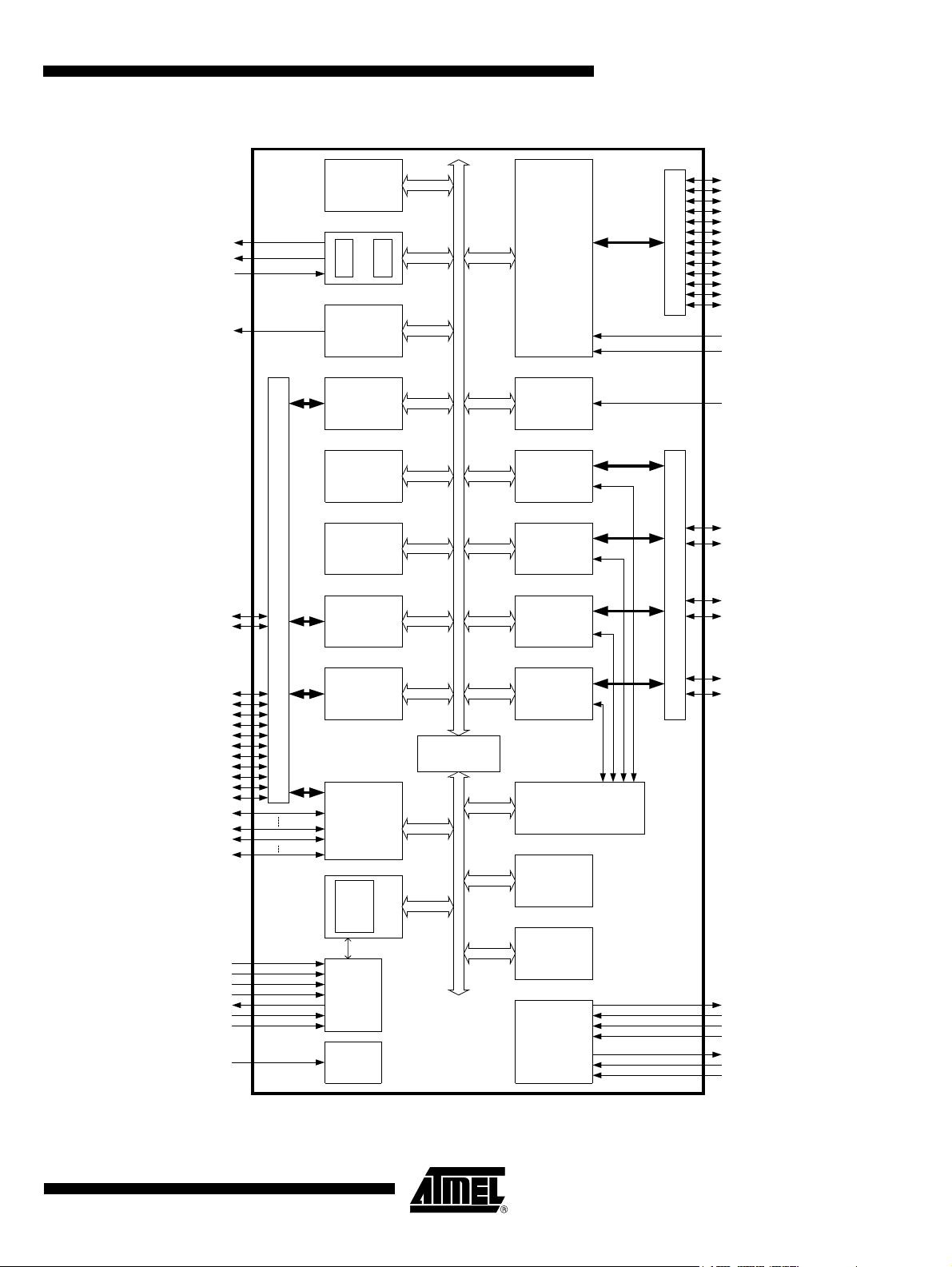
Figure 1-1. Block Diagram
nSHDN
nSLEEP
CLK32768
RF_ON
RTC
Power
ATR0620 [Preliminary]
P29/GPSMODE10
GPS
Accelerator
PIO2
GPS
Correlators
Manage-
ment
SRAM
Controller
P27/GPSMODE7
P26/GPSMODE5
P25/GPSMODE3
P24/GPSMODE2
P23/GPSMODE4
P20/TIMEPULSE
P19/GPSMODE9
P17/GPSMODE1
P14/GPSMODE0
P13/GPSMODE11
P12/GPSMODE8
P1/GPSMODE6
SIGLO
SIGHI
P11/EXTINT2
P9/EXTINT0
P16/NWD_OVF
P30/BOOT_MODE0
P28/EM_A20
P10/EM_A0/NLB
P8/PDSR8
P7/NUB/NWR1
P6/NOE/NRD
P5/NWE/NWR0
P4/nCS0
P3/nCS1
P2/BOOT_MODE1
EM_A19
EM_A1
EM_DA15
EM_DA0
PWM
Generator
Clock
Manager
(CLM)
CLK23
APB
PIO2
Controller
P21/TXD2
P22/RXD2
Special
Function
PIO2
Interrupt
Controller
Advanced
Watchdog
(EBI)
Interface to
Off-Chip Memory
B
RID
E
G
USART0 USART1 USART2 SPI
PDC2
PIO2
P18/TXD1
P31/RXD1
P15/TXD0
P0/RXD0
4574CS–GPS–05/05
DBG_EN
TEST_MODE
nTRST
TDO
TCK
TMS
nRESET
288K
ASB
ROM
ICE
Embedded
ARM7TDMI
128K
SRAM
TDI
JTAG
Con-
Reset
VBAT18_O
VBAT
VBAT18_I
Power
Supply
Manager
troller
LDOBAT_IN
LDO_OUT
LDO_IN
LDO_EN
3
Page 4

Table 1-1. Pin Configuration
Serial
Number BGA 100 CPGA 144 Pin Name
1 B6 C8 EM_DA0 (1) (1) (1) (1) (1)
2 B10 D13 EM_DA1 (1) (1) (1) (1) (1)
3 C7 B10 EM_DA2 (1) (1) (1) (1) (1)
4 C10 C15 EM_DA3 (1) (1) (1) (1) (1)
5 D10 F13 EM_DA4 (1) (1) (1) (1) (1)
6 E7 E15 EM_DA5 (1) (1) (1) (1) (1)
7 E9 F15 EM_DA6 (1) (1) (1) (1) (1)
8 B7 C9 EM_DA7 (1) (1) (1) (1) (1)
9 B8 B11 EM_DA8 (1) (1) (1) (1) (1)
10 A9 A14 EM_DA9 (1) (1) (1) (1) (1)
11 C8 B12 EM_DA10 (1) (1) (1) (1) (1)
12 B9 B13 EM_DA11 (1) (1) (1) (1) (1)
13 D8 E13 EM_DA12 (1) (1) (1) (1) (1)
14 C9 C14 EM_DA13 (1) (1) (1) (1) (1)
15 D9 D15 EM_DA14 (1) (1) (1) (1) (1)
16 E8 G14 EM_DA15 (1) (1) (1) (1) (1)
17 K5 N9 P15 TXD0 (1) TXD0 (1) MSOUT
18 K9 P14 P0 RXD0 RXD0 (1) (1) (1)
19 J5 Q10 P14 GPSMODE4 SCK0 SCK0 (1) GPS_MON5
20 K4 Q7 P18 TXD1 (1) TXD1 (1) NUB/NWR1
21 H9 N15 P31 RXD1 RXD1 (1) (1) (1)
22 J4 P8 P17 GPSMODE5 SCK1 SCK1 (1) GPS_MON6
23 F9 H14 SIGHI (1) (1) (1) (1) (1)
24 E10 G13 SIGLO (1) (1) (1) (1) (1)
25 J9 N14 XT_IN (1) (1) (1) (1) (1)
26 J10 P15 XT_OUT (1) (1) (1) (1) (1)
27 J6 Q11 nSLEEP (1) (1) (1) (1) (1)
28 G9 J13 CLK23 (1) (1) (1) (1) (1)
29 G5 N8 P30 BOOT_MODE0 (1) NWD_OVF (1) GPS_MON0
30 G4 P7 P2 BOOT_MODE1 (1) 1PPS (1) GPS_MON1
31 J1 P2 TMS (1) (1) (1) (1) (1)
32 J3 P6 TCK (1) (1) (1) (1) (1)
33 J2 P4 TDI (1) (1) (1) (1) (1)
34 K2 Q3 nTRST (1) (1) (1) (1) (1)
35 K3 N6 TDO (1) (1) (1) (1) (1)
36 F4 N1 TEST_MODE (1) (1) (1) (1) (1)
37 H4 N7 DBG_EN (1) (1) (1) (1) (1)
38 K6 N10 RF_ON (1) (1) (1) (1) (1)
39 C4 B3 nRESET (1) (1) (1) (1) (1)
40 G7 L14 nSHDN (1) (1) (1) (1) (1)
41 A6 B8 EM_A1 (1) (1) (1) (1) (1)
42 A5 A6 EM_A2 (1) (1) (1) (1) (1)
43 A4 A5 EM_A3 (1) (1) (1) (1) (1)
44 A2 C3 EM_A4 (1) (1) (1) (1) (1)
45 A3 C5 EM_A5
Firmware
Label
Note: 1. No selection option for PIO.
PIO Bank A PIO Bank B
IOIO
4
ATR0620 [Preliminary]
4574CS–GPS–05/05
Page 5

ATR0620 [Preliminary]
Table 1-1. Pin Configuration (Continued)
Serial
Number BGA 100 CPGA 144 Pin Name
46 B5 B7 EM_A6 (1) (1) (1) (1) (1)
47 B4 A3 EM_A7 (1) (1) (1) (1) (1)
48 B2 B1 EM_A8 (1) (1) (1) (1) (1)
49 D4 F2 EM_A9 (1) (1) (1) (1) (1)
50 C2 F3 EM_A10 (1) (1) (1) (1) (1)
51 D6 A9 EM_A11 (1) (1) (1) (1) (1)
52 D7 C10 EM_A12 (1) (1) (1) (1) (1)
53 C3 C1 EM_A13 (1) (1) (1) (1) (1)
54 C1 E2 EM_A14 (1) (1) (1) (1) (1)
55 D5 A4 EM_A15 (1) (1) (1) (1) (1)
56 C6 C7 EM_A16 (1) (1) (1) (1) (1)
57 F8 H13 EM_A17 (1) (1) (1) (1) (1)
58 B3 C4 EM_A18 (1) (1) (1) (1) (1)
59 C5 C6 EM_A19 (1) (1) (1) (1) (1)
60 E5 Q1 VDD18_R (1) (1) (1) (1) (1)
61 E6 A1 VDD18_B (1) (1) (1) (1) (1)
62 F7 K15 VDD18_L2 (1) (1) (1) (1) (1)
63 F6 A15 VDD18_L1 (1) (1) (1) (1) (1)
64 J7 P13 VBAT (1) (1) (1) (1) (1)
65 A1 D3 GND_R (1) (1) (1) (1) (1)
66 A10 C12 GND_B (1) (1) (1) (1) (1)
67 K1 N4 GND_T (1) (1) (1) (1) (1)
68 F10 J15 GND_L (1) (1) (1) (1) (1)
69 K10 M13 GND_BAT (1) (1) (1) (1) (1)
70 H1 N2 P24 GPSMODE8 MOSI MOSI (1) GPS_MON2
71 D1 G3 P25 GPSMODE9 MISO MISO (1) GPS_MON3
72 H3 P5 P23 GPSMODE7 SCK SCK (1) MCLK_OUT
73 G8 M15 P26 GPSMODE10 NSS NPCS0 (1) GPS_MON4
74 J8 N13 P9 GPSMODE1 EXTINT0 (1) (1) EM_A0/NLB
75 H7 N12 LDO_EN (1) (1) (1) (1) (1)
76 H6 Q13 LDO_OUT (1) (1) (1) (1) (1)
77 H5 P9 P3 (OH) nCS1 (1) nCS1 (1) AGCOUT0
78 A7 B9 P4 (OH) nCS0 (1) nCS0 (1) (1)
79 B1 D2 P5 (OH) NWE/NWR0 (1) NWE/NWR0 (1) (1)
80 A8 A13 P6 (OH) NOE/NRD (1) NOE/NRD (1) (1)
81 K7 P12 LDO_IN (1) (1) (1) (1) (1)
82 D2 G1 P7 (OH) NUB/NWR1 (1) NUB/NWR1 (1) (1)
83 E4 H2 P10 (OH) EM_A0/NLB (1) EM_A0/NLB (1) MCLK_OUT
84 H10 L13 P11 EM_A21 EXTINT2 (1) (1) EM_A21
85 G2 L3 P8 OUT (RFU) (1) AGCOUT0 (1) GPS_MON10
86 E1 H3 P16 NWD_OVF SIGHI2 (1) (1) NWD_OVF
87 F1 J2 P19 GPSMODE6 SIGLO2 (1) (1) EM_A20
88 G3 M3 P1 GPSMODE0 (1) AGCOUT1 (1) GPS_MON7
89 K8 Q14 LDOBAT_IN (1) (1) (1) (1) (1)
90 F2 K3 P21 TXD2 (1) TXD2 (1) EM_A22
91 H8 M14 P22 RXD2 RXD2 (1) (1) EM_A23
Firmware
Label
Note: 1. No selection option for PIO.
PIO Bank A PIO Bank B
IOIO
4574CS–GPS–05/05
5
Page 6

Table 1-1. Pin Configuration (Continued)
Serial
Number BGA 100 CPGA 144 Pin Name
92 H2 N3 P20 1PPS SCK2 SCK2 (1) 1PPS
93 E2 J3 P27 GPSMODE11 (1) NPCS1 (1) GPS_MON11
94 G1 M1 P28 EM_A20 (1) NPCS2 (1) EM_A20
95 E3 K1 P29 GPSMODE12 (1) NPCS3 (1) MSOUT
96 F3 L1 P12 GPSMODE2 (1) nCS2 (1) GPS_MON8
97 G10 K13 P13 GPSMODE3 EXTINT1 nCS3 (1) GPS_MON9
98 G6 N11 VBAT18_O (1) (1) (1) (1) (1)
99 F5 Q15 VBAT18_I (1) (1) (1) (1) (1)
100 D3 G2 TOUT1 (1) APB_SELECT (1) (1) (1)
101 (1) C13 EM_DA16 (1) (1) (1) (1) (1)
102 (1) E3 EM_DA17 (1) (1) (1) (1) (1)
103 (1) D14 EM_DA18 (1) (1) (1) (1) (1)
104 (1) E1 EM_DA19 (1) (1) (1) (1) (1)
105 (1) F14 EM_DA20 (1) (1) (1) (1) (1)
106 (1) H1 EM_DA21 (1) (1) (1) (1) (1)
107 (1) H15 EM_DA22 (1) (1) (1) (1) (1)
108 (1) K2 EM_DA23 (1) (1) (1) (1) (1)
109 (1) J14 EM_DA24 (1) (1) (1) (1) (1)
110 (1) M2 EM_DA25 (1) (1) (1) (1) (1)
111 (1) P1 EM_DA26 (1) (1) (1) (1) (1)
112 (1) Q2 EM_DA27 (1) (1) (1) (1) (1)
113 (1) B2 EM_DA28 (1) (1) (1) (1) (1)
114 (1) A2 EM_DA29 (1) (1) (1) (1) (1)
115 (1) B4 EM_DA30 (1) (1) (1) (1) (1)
116 (1) B5 EM_DA31 (1) (1) (1) (1) (1)
117 (1) Q6 TMON0 (1) (1) (1) (1) (1)
118 (1) Q8 TMON1 (1) (1) (1) (1) (1)
119 (1) Q9 TMON2 (1) (1) (1) (1) (1)
120 (1) P10 TMON3 (1) (1) (1) (1) (1)
121 (1) P11 TMON4 (1) (1) (1) (1) (1)
122 (1) Q12 TMON5 (1) (1) (1) (1) (1)
123 (1) L15 TMON6 (1) (1) (1) (1) (1)
124 (1) L2 TMON7 (1) (1) (1) (1) (1)
125 (1) J1 TMON8 (1) (1) (1) (1) (1)
126 (1) G15 TMON9 (1) (1) (1) (1) (1)
127 (1) F1 TMON10 (1) (1) (1) (1) (1)
128 (1) E14 TMON11 (1) (1) (1) (1) (1)
129 (1) D1 TMON12 (1) (1) (1) (1) (1)
130 (1) B15 TMON13 (1) (1) (1) (1) (1)
131 (1) C2 TMON14 (1) (1) (1) (1) (1)
132 (1) B14 TMON15 (1) (1) (1) (1) (1)
133 (1) C11 TMON16 (1) (1) (1) (1) (1)
134 (1) A12 TMON17 (1) (1) (1) (1) (1)
135 (1) A11 TMON18 (1) (1) (1) (1) (1)
136 (1) A10 TMON19 (1) (1) (1) (1) (1)
137 (1) A8 TMON20 (1) (1) (1) (1) (1)
Firmware
Label
Note: 1. No selection option for PIO.
PIO Bank A PIO Bank B
IOIO
6
ATR0620 [Preliminary]
4574CS–GPS–05/05
Page 7

ATR0620 [Preliminary]
Table 1-1. Pin Configuration (Continued)
Serial
Number BGA 100 CPGA 144 Pin Name
138 (1) A7 TMON21 (1) (1) (1) (1) (1)
139 (1) B6 TMON22 (1) (1) (1) (1) (1)
140 (1) Q5 TMON23 (1) (1) (1) (1) (1)
141 (1) Q4 TMON24 (1) (1) (1) (1) (1)
142 (1) N5 TMON25 (1) (1) (1) (1) (1)
143 (1) P3 TMON26 (1) (1) (1) (1) (1)
144 (1) K14 POR_VEXT (1) (1) (1) (1) (1)
Firmware
Label
Note: 1. No selection option for PIO.
Table 1-2. Pin Description
Module Name
Function
EM_A0 – 23 Address bus Output – All valid after reset
EM_DA0 – 31 Data bus I/O – –
NCS0 – NCS3 Chip select I/O Low –
NWR0 Lower byte 0 write signal I/O Low Used in byte write option
NWR1 Lower byte 0 write signal I/O Low Used in byte write option
NRD Read signal I/O Low Used in byte write option
EBI
NWE Write enable I/O Low Used in byte select option
NOE Output enable I/O Low Used in byte select option
NUB Upper byte select (16-bit SRAM) I/O Low Used in byte select option
NLB Lower byte select (16-bit SRAM) Output Low Used in byte write option
NWAIT Wait signal I/O Low –
BOOT_MODE0 Boot mode input I/O – PIO-controlled after reset, pull up
BOOT_MODE1 Boot mode input I/O – PIO-controlled after reset, pull down
TXD0-2 Transmit data output I/O – PIO-controlled after reset
USART
RXD0-2 Receive data input I/O – PIO-controlled after reset
SCK0-2 External serial clock I/O – PIO-controlled after reset
AIC EXTINT0-2 External interrupt request I/O High/Low PIO-controlled after reset
PWM AGCOUT0-1 Automatic gain control Output – PIO-controlled after reset
PMC RF_ON – – – ATR0600
nSleep Clear sleep output (AF-LDO) Output Low PIO-controlled after reset
RTC
nSHDN Clear sleep output (1.8LDO) I/O Low PIO-controlled after reset
XT_IN Oscillator input Input – OSC
XT_OUT Oscillator output Output – OSC
SCK SPI clock I/O – PIO-controlled after reset
SPI
MOSI Master out slave in I/O – PIO-controlled after reset
MISO Master in slave out I/O – PIO-controlled after reset
NPCS0-3 Slave select I/O Low PIO-controlled after reset
WD NWD_OVF Watchdog timer overflow I/O – PIO-controlled after reset
PIO PDSR0-31 Programmable I/O port I/O – Input after reset
Type Active Level Comment
PIO Bank A PIO Bank B
IOIO
4574CS–GPS–05/05
7
Page 8

Table 1-2. Pin Description (Continued)
Module Name
GPSMODE0-12 GPS mode I/O – PIO-controlled after reset
SIGHI – Input – –
SIGLO – Input – –
GPS
JTAG/
ICE
CLOCK
RESET nReset Reset input Input Low –
POWER
LDOBAT
LDO
TEST
SIGHI2 – Input – –
SIGLO2 – Input – –
1PPS – Output – –
MSOUT – Output – –
GPS_MON0-11 GPS monitor I/O – –
TMS Test mode select Input – Pull down
TDI Test data in Input – Pull down
TDO Test data out Output – –
TCK Test clock Input – Pull down
NTRST Test reset input Input Low Pull down
DBG_EN Debug enable Input – Pull down
CLK23 Clock input Input – Schmitt trigger
MCLK_OUT Master clock output Output – –
VDD18 – Power – –
GND – Power – –
VBAT18_I – IN Power – Backup power In
LDOBAT_IN – Power – –
VBAT – Power – –
VBAT18_O – Out – Backup power out
LDO_IN LDO in Power – –
LDO_OUT LDO out Power – –
LDO_EN LDO enable Input – –
TEST_MODE Test mode select Input – Production test
POR_VEXT Test input Input – For POR18 test
TMON0-26 Test monitor output Output – Debug package
TOUT1/APB_Select Test output Output – –
Function
Type Active Level Comment
8
ATR0620 [Preliminary]
4574CS–GPS–05/05
Page 9

2. Architecture Overview
The ATR0620 architecture consists of two main buses, the Advanced System Bus (ASB) and
the Advanced Peripheral Bus (APB). The ASB is designed for maximum performance. It interfaces the processor with the on-chip 32-bit memories and the external memories and devices by
means of the External Bus Interface (EBI). The APB is designed for accesses to on-chip peripherals and is optimized for low power consumption. The AMBA bridge provides an interface
between the ASB and the APB.
An on-chip Peripheral Data Controller (PDC2) transfers data between the on-chip USARTs/SPI
and the on- and off-chip memories without processor intervention. Most importantly, the PDC2
removes the processor interrupt handling overhead and significantly reduces the number of
clock cycles required for a data transfer. It can transfer up to 64 K continuous bytes without
reprogramming the starting address. As a result, the performance of the microcontroller is
increased and the power consumption reduced.
The ATR0620 peripherals are designed to be easily programmable with a minimum number of
instructions. Each peripheral has a 16-Kbyte address space allocated in the upper 3 M bytes of
the 4-GB address space. Except for the interrupt controller, the peripheral base address is the
lowest address of its memory space. The peripheral register set is composed of control, mode,
data, status and interrupt registers.
To maximize the efficiency of bit manipulation, frequently-written registers are mapped into three
memory locations. The first address is used to set the individual register bits, the second resets
the bits and the third address reads the value stored in the register. A bit can be set or reset by
writing a one to the corresponding position at the appropriate address. Writing a zero has no
effect. Individual bits can thus be modified without having to use costly read-modify-write and
complex bit-manipulation instructions.
ATR0620 [Preliminary]
3. PDC2
All of the external signals of the on-chip peripherals are under the control of the parallel I/O controller. The PIO2 controller can be programmed to insert an input filter on each pin or generate
an interrupt on a signal change. After reset, the user must carefully program the PIO2 controller
in order to define which peripheral signals are connected with off-chip logic.
The ARM7TDMI processor operates in little-endian mode in the ATR0620 GPS baseband. The
processor’s internal architecture and the ARM and Thumb instruction sets are described in the
ARM7TDMI data sheet. The memory map and the on-chip peripherals are described in detail in
the ATR0620 data sheet. The electrical and mechanical characteristics are also documented in
the ATR0620 data sheet.
The ARM standard In-Circuit Emulation (ICE) debug interface is supported via the ICE port of
the ATR0620.
The ATR0620 has an 8-channel PDC2 dedicated to the three on-chip USARTs and to the SPI.
One PDC2 channel is connected to the receiving channel and one to the transmitting channel of
each peripheral.
The user interface of a PDC2 channel is integrated in the memory space of each USART channel and in the memory space of the SPI. It contains a 32-bit address pointer register and a 16-bit
count register. When the programmed data is transferred, an end-of-transfer interrupt is generated by the corresponding peripheral. See the USART section and the SPI section for more
details on PDC2 operation and programming.
4574CS–GPS–05/05
9
Page 10

4. EBI: External Bus Interface
The EBI generates the signals that control the access to the external memory or peripheral
devices. The EBI is fully programmable and can address up to 64 bytes. It has four chip selects
and a 20-bit address bus.
The 16-bit data bus can be configured to interface with 8- or 16-bit external devices. Separate
read and write control signals allow for direct memory and peripheral interfacing. The EBI supports different access protocols, allowing single clock cycle memory accesses.
The main features are:
• External memory mapping
• 4 active low chip select lines
• 8- or 16-bit data bus
• Byte write or byte select lines
• User interface for remap function of boot memory
• Two different read protocols
• Programmable wait state generation
• Programmable data float time
• Programmable write protection for each memory bank
5. AIC: Advanced Interrupt Controller
The ATR0620 has an 8-level priority, individually maskable, vectored interrupt controller. This
feature substantially reduces the software and real time overhead in handling internal and external interrupts.
The interrupt controller is connected to the NFIQ (fast interrupt request) and the NIRQ (standard
interrupt request) inputs of the ARM7TDMI processor. The processor’s NFIQ line can only be
asserted by the external fast interrupt request input: FIQ. The NIRQ line can be asserted by the
interrupts generated by the on-chip peripherals and the external interrupt request lines: IRQ0 to
IRQ3.
An 8-level priority encoder allows the customer to define the priority between the different NIRQ
interrupt sources. Internal sources are programmed to be level sensitive or edge triggered.
External sources can be programmed to be positive or negative edge triggered or high- or lowlevel sensitive.
6. PIO2: Parallel I/O Controller
The ATR0620 features 32 programmable I/O lines. The I/O lines are multiplexed with on-chip
peripheral I/O signals in order to optimize the use of available package pins. The PIO2 controller
provides an internal interrupt signal to the Advanced Interrupt Controller (AIC).
10
ATR0620 [Preliminary]
4574CS–GPS–05/05
Page 11

ATR0620 [Preliminary]
7. USART2: Universal Synchronous/ Asynchronous Receiver/Transmitter
The ATR0620 provides three identical, full-duplex, universal synchronous/asynchronous
receiver/transmitters that interface to the APB and are connected to the peripheral data
controller.
The main features are:
• Programmable baud rate generator
• Parity, framing and overrun error detection
• Line break generation and the detection
• Automatic echo, local loopback and remote loopback channel modes
• Multi-drop mode: address detection and generation
• Interrupt generation
• Two dedicated peripheral data controller channels
• 5-, 6-, 7-, 8-, and 9-bit character length
• Protocol ISO 7816 T = 0 and T = 1
8. SPI: Serial Peripheral Interface
The ATR0620 features an SPI, which provides communication with external devices in master or
slave mode. The SPI has four external chip selects that can be connected to up to 15 devices.
The data length is programmable from 8- to 16-bit. The PDC is used to move data directly
between memory and SPI without CPU intervention for maximum real-time processing
throughput.
9. WD: Watchdog Timer
The ATR0620 features an internal watchdog timer, which can be used to guard against system
lock-up if the software becomes trapped in a deadlock. The watchdog timer can be programmed
to generate an interrupt or an internal reset.
10. PMC: Power Manager Controller
The power management controller allows optimization of power consumption. The PMC
enables/disables the clock inputs to most of the peripherals as well as to the ARM processor.
When the ARM clock is disabled, the current instruction is processed before the clock is
stopped. The clock can be re-enabled by any enabled interrupt or by a hardware reset. When a
peripheral clock is disabled, the clock is immediately stopped. When the clock is re-enabled the
peripheral resumes action where it left off.
Due to the static nature of the design, the contents of the on-chip RAM and registers for which
the clocks are disabled remain unchanged.
11. CLM: Clock Manager
In addition to the Power Management Controller (PMC) the Clock Manager (CLM) is another
possibility to reduce power consumption. The clock manager provides fixed divided clocks for
the USARTs, SPI and watchdog timer and generates the master clock which can be divided.
The master clock is programmable for frequencies between 175 kHz and 23.1 MHz.
4574CS–GPS–05/05
11
Page 12

12. SF: Special Function
The ATR0620 provides registers that implement the following special functions:
• Chip identification
• RESET status
13. PWM
The PWM includes two PWM channels. They can be programmed separately. It is possible to
generate an output voltage range from 0 to (255/256) × VDD18.
14. RTC
The RTC provides the time in GPS format. The structure of the GPS system time: zero point is
midnight Universal Time (UT) 5
and the 15-bit fractional part of a second are counted. Each week has 604800 seconds (GPS
system time does not count leap seconds. Therefore, compared to UT, the GPS time is shifted
some seconds).
Additional the RTC provides a programmable interrupt (maximum period: one week).
15. GPS Correlator
The GPS correlator incorporates 16 GPS channels and provides all the functionality required for
sampling, down-converting and correlating GPS signals.
th/6th
of January 1980. From the zero point weeks, time of week
The GPS correlator processes GPS signal data to acquire the GPS satellite signals using a
model of the satellite codes and multiply/accumulate circuits (correlators) to spread the signal to
a bandwidth low enough to detect it above thermal noise.
16. GPS Accelerator
The ATR0620 features an accelerator which reduces the time to identify the correct GPS signal.
12
ATR0620 [Preliminary]
4574CS–GPS–05/05
Page 13

ATR0620 [Preliminary]
17. Ordering Information
Extended Type Number Package Remarks
ATR0620-100 CTBGA100 9 mm × 9 mm, 0.80 mm pitch
ATR0620-144 CPGA144 Debug package
18. Package Outline CTBGA100
TOP VIEW SIDE VIEW
1.10 ± 0.10
9.00 ± 0.05
9.00 ± 0.05
0.30 ± 0.05
0.40 Dia. TYP
0.60 ± 0.05
0.80 ± 0.050.90 ± 0.05
10
BOTTOM VIEW
A1 BALL PAD CORNER
0.90 ± 0.05
231564897
A
B
C
D
E
F
G
H
J
K
0.80 ± 0.05
4574CS–GPS–05/05
13
Page 14

19. Package CPGA144
TOP VIEW
1.575 ± 0.16
1.575 ± 0.16
BOTTOM VIEW
1.400 ± 0.012
0.100 TYP
SIDE VIEW
0.090 ± 0.009
0.018 ± 0.002
A
B
C
D
E
F
G
H
J
K
L
M
N
P
R
123456789101112131415
14
ATR0620 [Preliminary]
4574CS–GPS–05/05
Page 15

Atmel Corporation Atmel Operations
2325 Orchard Parkway
San Jose, CA 95131, USA
Tel: 1(408) 441-0311
Fax: 1(408) 487-2600
Regional Headquarters
Europe
Atmel Sarl
Route des Arsenaux 41
Case Postale 80
CH-1705 Fribourg
Switzerland
Tel: (41) 26-426-5555
Fax: (41) 26-426-5500
Asia
Room 1219
Chinachem Golden Plaza
77 Mody Road Tsimshatsui
East Kowloon
Hong Kong
Tel: (852) 2721-9778
Fax: (852) 2722-1369
Japan
9F, Tonetsu Shinkawa Bldg.
1-24-8 Shinkawa
Chuo-ku, Tokyo 104-0033
Japan
Tel: (81) 3-3523-3551
Fax: (81) 3-3523-7581
Memory
2325 Orchard Parkway
San Jose, CA 95131, USA
Tel: 1(408) 441-0311
Fax: 1(408) 436-4314
Microcontrollers
2325 Orchard Parkway
San Jose, CA 95131, USA
Tel: 1(408) 441-0311
Fax: 1(408) 436-4314
La Chantrerie
BP 70602
44306 Nantes Cedex 3, France
Tel: (33) 2-40-18-18-18
Fax: (33) 2-40-18-19-60
ASIC/ASSP/Smart Cards
Zone Industrielle
13106 Rousset Cedex, France
Tel: (33) 4-42-53-60-00
Fax: (33) 4-42-53-60-01
1150 East Cheyenne Mtn. Blvd.
Colorado Springs, CO 80906, USA
Tel: 1(719) 576-3300
Fax: 1(719) 540-1759
Scottish Enterprise Technology Park
Maxwell Building
East Kilbride G75 0QR, Scotland
Tel: (44) 1355-803-000
Fax: (44) 1355-242-743
RF/Automotive
Theresienstrasse 2
Postfach 3535
74025 Heilbronn, Germany
Tel: (49) 71-31-67-0
Fax: (49) 71-31-67-2340
1150 East Cheyenne Mtn. Blvd.
Colorado Springs, CO 80906, USA
Tel: 1(719) 576-3300
Fax: 1(719) 540-1759
Biometrics/Imaging/Hi-Rel MPU/
High Speed Converters/RF Datacom
Avenue de Rochepleine
BP 123
38521 Saint-Egreve Cedex, France
Tel: (33) 4-76-58-30-00
Fax: (33) 4-76-58-34-80
Literature Requests
www.atmel.com/literature
Disclaimer: The information in this document is provided in connection with Atmel products. No license, express or implied, by estoppel or otherwise, to any
intellectual property right is granted by this document or in connection with the sale of Atmel products. EXCEPT AS SET FORTH IN ATMEL’S TERMS AND CONDI-
TIONS OF SALE LOCATED ON ATMEL’S WEB SITE, ATMEL ASSUMES NO LIABILITY WHATSOEVER AND DISCLAIMS ANY EXPRESS, IMPLIED OR STATUTORY
WARRANTY RELATING TO ITS PRODUCTS INCLUDING, BUT NOT LIMITED TO, THE IMPLIED WARRANTY OF MERCHANTABILITY, FITNESS FOR A PARTICULAR
PURPOSE, OR NON-INFRINGEMENT. IN NO EVENT SHALL ATMEL BE LIABLE FOR ANY DIRECT, INDIRECT, CONSEQUENTIAL, PUNITIVE, SPECIAL OR INCIDENTAL DAMAGES (INCLUDING, WITHOUT LIMITATION, DAMAGES FOR LOSS OF PROFITS, BUSINESS INTERRUPTION, OR LOSS OF INFORMATION) ARISING OUT
OF THE USE OR INABILITY TO USE THIS DOCUMENT, EVEN IF ATMEL HAS BEEN ADVISED OF THE POSSIBILITY OF SUCH DAMAGES. Atmel makes no
representations or warranties with respect to the accuracy or completeness of the contents of this document and reserves the right to make changes to specifications
and product descriptions at any time without notice. Atmel does not make any commitment to update the information contained herein. Atmel’s products are not
intended, authorized, or warranted for use as components in applications intended to support or sustain life.
© Atmel Corporation 2005. All rights reserved. Atmel®, logo and combinations thereof, Everywhere You Are® and others, are registered trade-
marks or trademarks of Atmel Corporation or its subsidiaries. Other terms and product names may be trademarks of others.
Printed on recycled paper.
4574CS–GPS–05/05
 Loading...