

Page 1
Features
• Low Noise Figure
• High Small Signal Gain
• Single +2.7 V Operation
• Power-up Control
• 50 Ω Output
• Unconditionally Stable
Benefits
• Low Power Consumption < 10 mW
• Very Small, PLLP6 Package (1.6 mm × 2.0 mm)
• Few External Components
Electrostatic sensiti ve device.
Observe precautions for handling.
Description
The ATR0610 is a 2.7-V GPS low-noise am pli fie r IC des ig ned for use in GP S a ppl ic ations. It uses a SiGe HBT die. The IC is 50-W matched on the output allowing the
device to be used with minimal external circuitr y. Its RF performance meets the
requirements for products designed to the GPS standard.
The ATR0610 gives excellent RF performance with low cu rrent c onsum ption re sultin g
in longer battery life times. The package has a small 1.6 mm ´ 2.0 mm footpr int t o
allow use in compact GPS receiver design.
2.7-V GPS
Low-noise
Amplifier
ATR0610
Preliminary
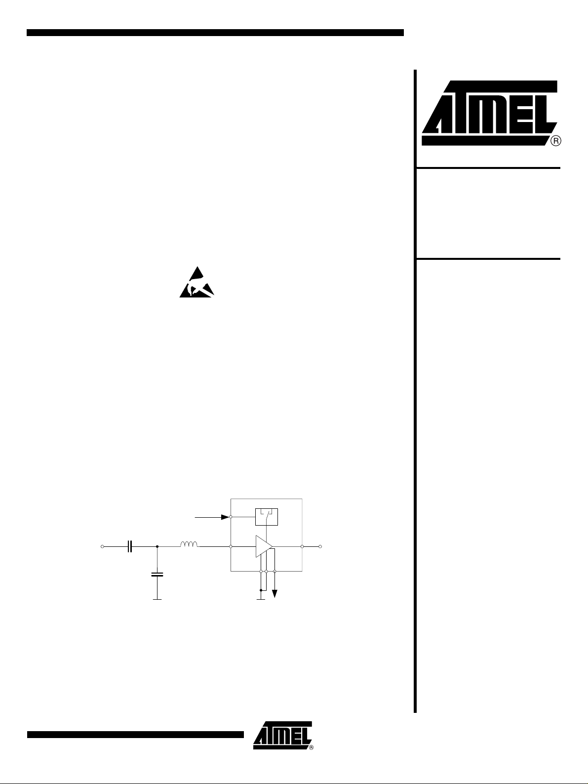
Figure 1. Block Diagram
Cblock = 1 nF
RF-Input RF-Output
Cshunt = 1.5 pF
P
U
Lseries = 3.9 nH
PU Mode PD Mode
ATR0610
GND VCC
Rev. 4573C–GPS–02/03
1
Page 2
Pin Description
Pin Symbol Function
1 VCC Supply voltage
2 RF_OUT Signal output
3 DC_GND Ground
4 RF_IN Input for received signal
5 RF_GND Ground for RF stage
6 PU Power up
Absolute Maximum Ratings
Parameters Symbol Value Unit
Supply voltage V
Power-up Voltage V
Input power P
Operating temperature T
Storage temperature T
CC
PU
in
op
stg
-0.3 to +3.7 V
-0.3 to +3.7 V
-5 dBm
-40 to +85 °C
-55 to +125 °C
Thermal Resistance
Parameters Symbol Value Unit
Thermal resistance R
th
TBD K/W
Electrical Characteristics
VCC = 2.7 V, VPU = 1.8 V, f = 1575 MHz, T
Minimum/maximum limits are at +25°C ambient temperature, unless otherwise specified.
No. Parameter s Test Conditi ons Pin Symbol Min. Typ. Max. Unit Type*
1 Operating frequency RF_IN f 1575.42 MHz D
2 Supply voltage VCC V
3 Operating current RF ON (V
4 Power-down current RF OFF(V
5 Small signal gain G 15 16 17 dB A
6 Minimum noise figure NF
Noise figure Using the prop osed input
7
Input referred 1dB
8
compression point
rd
Input 3
9
intercept point
Input 3
10
cept point (inband)
-order
rd
-order inter-
11 Input return loss RL
12 Output return loss RL
*) Type means: A = 100% tested, B = 100% correlation tested, C = Characterized on samples, D = Design parameter
matching (see Figure 1)
Caused by a DCS
blocker at 1710 MHz
f1 = 1750 MHz
f2 = 1925 MHz
f1 = 1575 MHz
f2 = 1577 MHz
= 25°C, Z
amb
= 1.8 V) VCC I 3 3.3 3.5 mA A
PU
= 0 V) VCC I
PU
= 50 W (see Figure 1)
load
CC
PD
min
2.733.3VC
500 nA A
1.5 dB C
NF 1.6 dB C
Icp1 -9 dBm A
IIP3 -1 dBm C
IIP3
out
inb
in
10 11 dB C
11 12 dB C
-3 dBm C
2
ATR0610
4573C–GPS–02/03
Page 3
Electrical Characteristics (Continued)
ATR0610
VCC = 2.7 V, VPU = 1.8 V, f = 1575 MHz, T
= 25°C, Z
amb
= 50 W (see Figure 1)
load
Minimum/maximum limits are at +25°C ambient temperature, unless otherwise specified.
No. Parameter s Test Conditi ons Pin Symbol Min. Typ. Max. Unit Type*
PU,high
PU,high
PU,low
PU,low
2
30 dB C
1.2 1.8 3.3 V C
01050µAC
00.20.4VC
0.7 µA C
13 Reverse isolation 1/|S12|
14 Control voltage Power-up mode PU V
15 Control current Power-up mode PU I
16 Control voltage Power-down mode PU V
17 Control current Power-down mode PU I
*) Type means: A = 100% tested, B = 100% correlation tested, C = Characterized on samples, D = Design parameter
4573C–GPS–02/03
3
Page 4

Measurement Results
Matched Device
(see Figure 1)
Figure 2. Gain and Maximum Available Gain
30.0
20.0
10.0
0.0
-10.0
-20.0
-30.0
Gain (dB)
-40.0
-50.0
-60.0
0 500 1000 1500 2000 2500 3000
Gmax
f (MHz)
Figure 3. Input and Output Return Loss
0.0
-5.0
-10.0
Gain
RLout
-15.0
RLin, RLout (dB)
-20.0
-25.0
0 500 1000 1500 2000 2500 3000
Figure 4. Reverse Transfer Function
0
-10
-20
-30
-40
-50
(dB)
-60
S12
-70
-80
-90
-100
0 500 1000 1500 2000 2500 3000
RLin
f (MHz)
f (MHz)
4
ATR0610
4573C–GPS–02/03
Page 5

Figure 5. K Factor ( => Unconditional Stability)
10.0
9.0
8.0
7.0
6.0
5.0
4.0
K Factor
3.0
2.0
1.0
0.0
0 500 1000 1500 2000 2500 3000
Table 1. Measured Scattering Parameters of Matched Device
(Given as Linear Magnitude and Phase in Degree)
ATR0610
f ( MHz)
f /MHz
|S
|
11
ϕ(S
)
11
|S
|
21
ϕ(S
)
21
|S
|
12
ϕ(S
)
12
|S
|
22
ϕ(S
22
)
K Factor
60 0.897 -9.9 0.06 -96.1702 0.0006 19.5 0.998 -6.6 13.5
120 0.891 -25.6 0.17 -98.98544 0.0008 84.2 0.996 -17.4 5.5
180 0.886 -37.4 0.26 -113.4846 0.0002 173.8 0.991 -26.1 43.3
240 0.891 -49.4 0.34 -128.3148 0.0008 -86.0 0.987 -34.4 10.1
300 0.894 -61.9 0.32 -145.6032 0.0021 -137.8 0.981 -42.8 6.5
360 0.890 -74.3 0.26 -128.5304 0.0014 153.2 0.979 -51.4 12.3
420 0.879 -86.0 0.41 -113.438 0.0022 149.7 0.973 -60.1 7.4
480 0.876 -97.1 0.62 -117.7927 0.0037 147.3 0.965 -69.3 4.4
540 0.872 -108.2 0.83 -125.7797 0.0039 143.4 0.958 -78.0 3.8
600 0.869 -118.8 1.07 -135.3626 0.0043 142.5 0.948 -87.1 3.4
660 0.872 -129.8 1.34 -144.9783 0.0063 130.7 0.935 -96.9 2.5
720 0.874 -140.7 1.66 -155.2931 0.0101 127.3 0.920 -106.6 1.7
780 0.878 -153.0 2.04 -168.018 0.0144 108.8 0.893 -116.9 1.5
840 0.813 -165.3 2.30 177.8467 0.0152 73.6 0.863 -126.3 2.0
900 0.806 -172.6 2.64 169.357 0.0126 71.9 0.853 -137.2 2.1
960 0.813 176.5 3.17 157.1773 0.0185 79.4 0.817 -149.8 1.6
1020 0.809 164.4 3.78 143.6133 0.0237 67.9 0.767 -163.0 1.4
1080 0.785 150.1 4.34 128.2928 0.0318 51.1 0.693 -176.6 1.3
1140 0.732 135.5 4.93 111.4632 0.0399 35.3 0.598 168.3 1.3
1200 0.637 118.7 5.30 92.48291 0.0491 11.0 0.466 155.8 1.3
1260 0.522 107.6 5.32 76.71066 0.0494 -10.0 0.381 147.9 1.5
1320 0.378 98.0 5.24 63.20023 0.0517 -36.7 0.325 141.9 1.7
1380 0.311 108.3 5.33 56.22391 0.0385 -63.8 0.358 125.1 2.1
1440 0.325 97.5 6.14 41.04218 0.0326 -62.8 0.270 88.5 2.3
1500 0.287 88.9 6.51 25.58716 0.0307 -74.9 0.212 52.2 2.4
4573C–GPS–02/03
5
Page 6

Table 1. Measured Scattering Parameters of Matched Device
(Given as Linear Magnitude and Phase in Degree) (Continued)
f /MHz
|S
|
11
ϕ(S
)
11
|S
|
21
ϕ(S
)
21
|S
|
12
ϕ(S
)
12
|S
|
22
ϕ(S
22
)
K Factor
1560 0.257 73.3 6.77 8.313904 0.0320 -76.5 0.207 -1.0 2.2
1620 0.180 59.1 6.58 -8.583069 0.0355 -93.7 0.202 -46.0 2.1
1680 0.175 46.3 6.79 -22.98477 0.0281 -107.7 0.268 -62.3 2.5
1740 0.160 3.9 6.78 -40.46539 0.0263 -103.6 0.358 -81.5 2.4
1800 0.152 -43.9 6.33 -57.3143 0.0297 -112.5 0.411 -101.3 2.2
1860 0.187 -77.9 5.95 -73.04535 0.0288 -121.8 0.453 -116.8 2.2
1920 0.249 -104.8 5.58 -87.41135 0.0310 -132.7 0.471 -129.8 2.1
1980 0.314 -122.7 5.15 -100.7899 0.0285 -142.7 0.487 -139.2 2.3
2040 0.389 -137.6 4.71 -114.63 0.0307 -154.3 0.492 -150.3 2.1
2100 0.450 -151.0 4.33 -127.6309 0.0305 -171.1 0.476 -156.8 2.2
2160 0.514 -162.2 3.99 -138.8933 0.0328 175.1 0.452 -162.0 2.1
2220 0.564 -172.4 3.71 -151.1952 0.0333 148.3 0.443 -152.8 2.1
2280 0.621 179.3 3.45 -166.5967 0.0205 110.4 0.645 -158.2 2.5
2340 0.678 169.7 3.08 -178.6954 0.0100 118.3 0.708 -173.7 4.1
2400 0.722 160.6 2.66 170.4748 0.0071 129.9 0.722 175.9 5.7
2460 0.762 152.2 2.39 158.4146 0.0056 136.8 0.738 167.1 6.7
2520 0.793 144.0 2.14 148.5269 0.0042 129.5 0.742 158.8 8.7
2580 0.821 136.5 1.87 139.0457 0.0047 134.1 0.750 151.3 7.5
2640 0.839 129.4 1.65 127.6694 0.0032 158.1 0.762 143.8 11.3
2700 0.857 122.3 1.50 118.4024 0.0048 168.3 0.768 136.4 6.9
2760 0.876 115.8 1.30 109.0173 0.0047 173.3 0.774 129.3 7.1
2820 0.886 109.5 1.13 98.04062 0.0056 -171.8 0.775 121.4 6.3
2880 0.900 103.2 0.99 88.75305 0.0058 -173.3 0.775 113.9 6.2
2940 0.908 97.4 0.84 80.06287 0.0069 175.4 0.775 106.6 5.6
3000 0.914 91.3 0.71 69.79065 0.0086 167.6 0.761 98.8 5.2
Figure 6. Gain versus Blocker at 1710 MHz (Compression)
20.0
18.0
16.0
14.0
12.0
10.0
8.0
Gain (dB)
6.0
4.0
2.0
0.0
-50 -40 -30 -20 -10 0 10
6
ATR0610
CW blocking power (dBm)
4573C–GPS–02/03
Page 7

Figure 7. Out of Band Intermodulation Product 3rd Order (IP3)
40.0
IP3
20.0
0.0
-20.0
-40.0
Pout ( dBm)
-60.0
-80.0
-50 -40 -30 -20 -10 0 10
Pin (dBm)
ATR0610
Figure 8. Inband Intermodulation Product 3
40.0
20.0
0.0
-20.0
-40.0
Pout (dBm)
-60.0
-80.0
-50 -40 -30 -20 -10 0 10
rd
Order (Inband IP3)
Pin (dBm)
Figure 9. Noise Figure without any De-embedding
3.0
2.5
2.0
Inband IP3
4573C–GPS–02/03
1.5
NF (dB)
1.0
0.5
0.0
1.25 1.38 1.50 1.63 1.75 1.88 2.00
f (GHz)
7
Page 8

Figure 10. Reference Planes of Unmatched Device
Unmatched Device
PU Mode PD Mode
ATR0610
RF-Output
GND VCC
RF-Input
P
U
Cblock = 1 nF
Port 1 Port 2
Table 2. Measured Scattering Parameters of Unmatched Device (De-embedded)
(Given as Linear Magnitude and Phase in Degree)
f/MHz |S11| ϕ(S11) |S21| ϕ(S21) |S12| ϕ(S12) |S22| ϕ(S22)
1.400 0.725 -116.0 6.04 132.8 0.028 63.1 0.400 104.5
1.425 0.712 -117.7 6.12 127.7 0.030 58.2 0.366 94.5
1.450 0.698 -119.3 6.17 122.6 0.031 53.0 0.332 83.6
1.475 0.682 -120.6 6.19 117.6 0.032 47.7 0.303 72.2
1.500 0.666 -122.0 6.18 112.7 0.033 42.0 0.278 60.2
1.525 0.647 -123.1 6.16 108.1 0.033 35.9 0.258 47.4
1.550 0.630 -123.9 6.10 103.8 0.034 29.5 0.244 35.0
1.575 0.610 -124.4 6.05 99.6 0.034 22.5 0.240 22.5
1.600 0.592 -124.6 5.98 95.8 0.034 15.9 0.240 10.8
1.625 0.573 -124.2 5.93 92.4 0.034 7.8 0.249 1.5
1.650 0.558 -123.3 5.92 89.4 0.032 -1.0 0.276 -7.1
1.675 0.552 -121.7 5.99 86.0 0.029 -9.0 0.315 -16.6
1.700 0.556 -120.5 6.05 82.0 0.026 -15.3 0.360 -27.3
1.725 0.565 -120.0 6.10 77.5 0.022 -18.7 0.404 -38.2
1.750 0.573 -120.1 6.10 72.9 0.020 -20.0 0.443 -48.6
Figure 11. Minimum Noise Figure NF
3.0
2.5
2.0
1.5
1.0
NFmin (dB)
0.5
0.0
1.4 1.5 1.6 1.7
8
ATR0610
(De-embedded)
min
f (GHz)
4573C–GPS–02/03
Page 9

Table 3. Raw Noise Data of Unmatched Device (de-embedded)
f/GHz NFmin/dB |Γopt| φ(Γopt) Rn/Ω
1.400 1.51 0.31 98.07 8.89
1.425 1.46 0.31 98.55 8.71
1.450 1.45 0.31 100.00 9.30
1.475 1.43 0.31 100.16 9.13
1.500 1.43 0.31 101.78 8.70
1.525 1.38 0.32 103.08 9.15
1.550 1.49 0.31 104.16 9.41
1.575 1.49 0.31 106.49 8.78
1.600 1.57 0.28 109.84 9.05
1.625 1.50 0.30 110.74 8.22
1.650 1.54 0.31 112.12 8.41
1.675 1.52 0.31 113.20 8.61
1.700 1.52 0.31 113.33 8.40
1.725 1.65 0.28 116.76 8.61
1.700 1.52 0.31 113.33 8.40
1.725 1.65 0.28 116.76 8.61
1.750 1.62 0.31 115.03 8.24
ATR0610
Figure 12. Schematic of Application Board
4573C–GPS–02/03
9
Page 10

Bill of Materials of Demo Board
Component Reference Vendor Part Number/Remark Value Size/Package
C1 1 nF 0402
C2 NPO 1.5 pF 0402
C3, C5 nc
C20 10 uF 3216
C23 100 nF 0402
L1 TOKO LL1005-FH3N9 3.9 nH 0402
L5, L8
R1 nc
R5, R7 1W 0402
Note: 1. Other sizes are possible.
Figure 13. Layout of Demo Board
Würth
Elektronik
WE74476401 1210
(1)
10
ATR0610
4573C–GPS–02/03
Page 11
Ordering Information
Extended Type Numb er Package Remarks
ATR0610-PQQ PLLP6 Area 1.6mm ´ 2.0 mm, 0.5 mm pitch
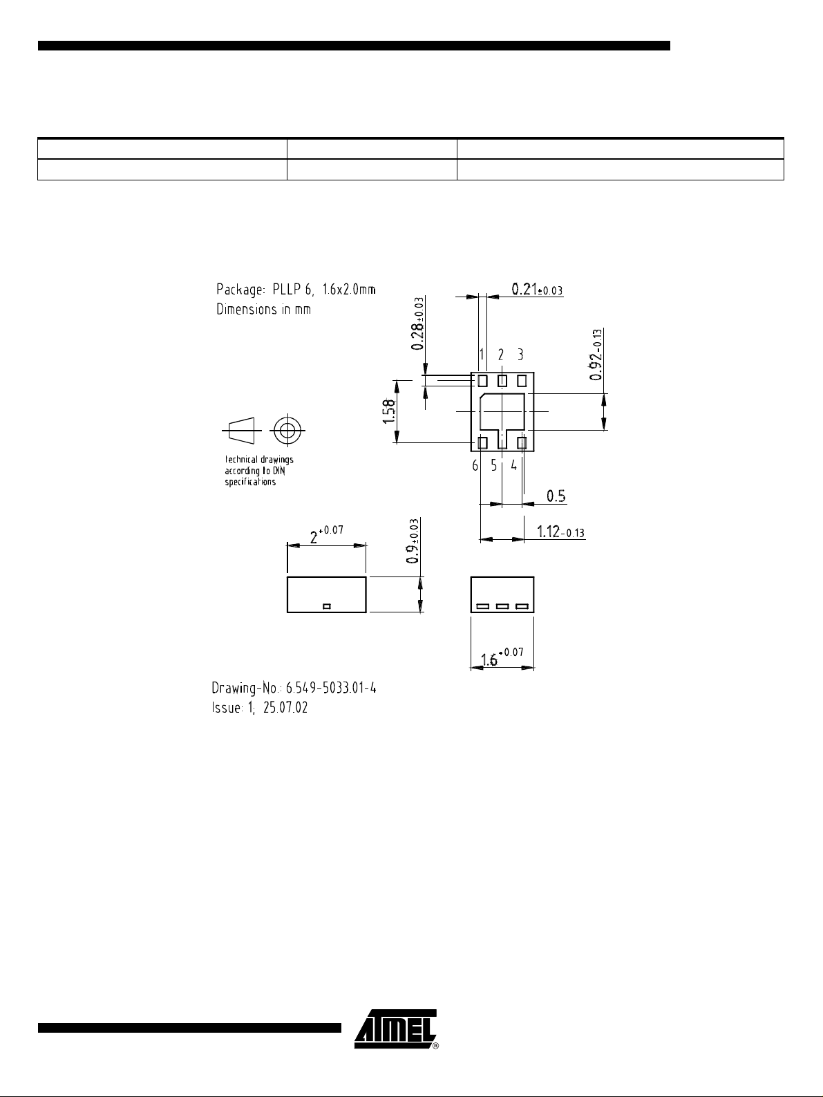
Package Information
ATR0610
4573C–GPS–02/03
11
Page 12

12
ATR0610
4573C–GPS–02/03
Page 13

Atmel Headquar ters Atmel Operati ons
Corporate Headquarters
2325 Orchard Parkway
San Jose, CA 95131
TEL 1(408) 441-0311
FAX 1(408) 487-2600
Europe
Atmel Sarl
Route des Arsenaux 41
Case Postale 80
CH-1705 Fribourg
Switzerland
TEL (41) 26-426-5555
FAX (41) 26-426-5500
Asia
Room 1219
Chinachem Gol den P laza
77 Mody Road Tsimhatsui
East Kowloon
Hong Kong
TEL (852) 2721-9778
FAX (852) 2722-1369
Japan
9F, Tonetsu Shinkawa Bldg.
1-24-8 Shin kawa
Chuo-ku, Tokyo 104-0033
Japan
TEL (81) 3- 3523-3 551
FAX (81) 3-3523-7581
Memory
2325 Orchard Parkway
San Jose, CA 95131
TEL 1(408) 441-0311
FAX 1(408) 436-4314
Microcontrollers
2325 Orchard Parkway
San Jose, CA 95131
TEL 1(408) 441-0311
FAX 1(408) 436-4314
La Chantrerie
BP 70602
44306 Nantes Cedex 3, France
TEL (33) 2-40-18-18-18
FAX (33) 2- 40-18- 19-6 0
ASIC/ASSP/Smart Cards
Zone Industrielle
13106 Rousset Cedex, France
TEL (33) 4-42-53-60-00
FAX (33) 4- 42-53- 60-0 1
1150 East Cheyenne Mtn. Blvd.
Colorado Springs, CO 80906
TEL 1(719) 576-3300
FAX 1(719) 540-1759
Scottish Enterprise Technology Park
Maxwell Building
East Kilbride G75 0QR, Scotland
TEL (44) 1355-803-000
FAX (44) 1355-242-743
RF/Automotive
Theresienstrasse 2
Postfach 3535
74025 Heilbro nn, Ge rmany
TEL (49) 71-31-67-0
FAX (49) 71-31-67-2340
1150 East Cheyenne Mtn. Blvd.
Colorado Springs, CO 80906
TEL 1(719) 576-3300
FAX 1(719) 540-1759
Biometrics/Imaging/Hi-Rel MPU/
High Speed Converters/RF Datacom
Avenue de Rochepleine
BP 123
38521 Saint-Egreve Cedex, France
TEL (33) 4-76-58-30-00
FAX (33) 4- 76-58- 34-8 0
e-mail
literature@atmel.com
Web Site
http://www.atmel.com
© Atmel Corporation 2003.
Atmel Corporation makes no warranty for the use of its products, other than those expressly contained in the Company’s standard warranty
which is detailed in Atmel’s Terms and Conditions located on the Company’s web site. The Company assumes no responsibility for any errors
which may appear in this document, reserves the right to change devices or specifications det ailed herein at any time without notice, and does
not make any commitment to update the information contained herein. No licenses to patents or other intellectual property of Atmel are granted
by the Company in connection with the sale of Atmel products, expressly or by implication. Atmel’s products are not authorized for use as critical
components in life support devices or systems.
Atmel® is the registered trademark of Atmel.
Other terms and product names may be the trademarks of others.
Printed on recycled paper.
4573C–GPS–02/03
xM
 Loading...