

Page 1
Features
•
Very Low Power Design (40 mW)
•
Single IF Architecture
•
Excellent Noise Performance
•
1.5-bit ADC On Chip
•
Small QFN Package (4 mm × 4 mm, 24 pins)
•
Highly integrated, Few External Components
•
Advanced BiCMOS Technology (UHF6s)
•
Non ESD Sensitive Device
1. Description
The ATR0601 is a single IF GPS front-end IC, designed to meet the requirements of
mobile and automotive applications. Excellent RF performance combined with low
noise figure enables high quality GPS solutions and it's very low power consumption
fits perfectly to portable devices. Featuring a balanced XTO and a fully integrated balanced frequency synthesizer, only few external components are required. The
ATR0601 offers a complete autonomous mode, utilizing the on chip AGC in closed
loop operation, to set the gain of the IF VGA. Alternatively, in combination with the
baseband processor ATR0621 the optimum gain of the IF VGA can be computed and
set by software, using the digital SDI interface.
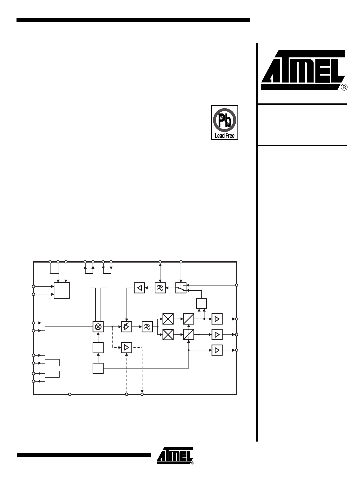
Figure 1-1. Block Diagram
GPS Front-end
IC
ATR0601
Preliminary
PUXTO
PURF
RF
NRF
XTO
NXTO
NX
MO
AGCO
EGC
SDI
1
A
D
A
D
SL
SH
SC
Rev. 4866A–GPS–08/05
VCC
VCC
VDIG
PMSS
Logic
X
GND
BP
NBP
VCO
XTO
PLL
BPI
NBPI
EST
Page 2
2. Pin Configuration
Figure 2-1. Pinning QFN24
SDI
NRF
EGC
RF
19
12
VCC
NC
18
17
16
15
14
13
PURF
PUXTO
NBPI
BPI
NBP
BP
VDIG
AGCO
NXTO
NX
XTO
SCSHSL
24
222120
23
1
2
3
4
X
5
6
7
VCC
Paddle
GND
91011
8
MO
TEST
Table 2-1. Pin Description
Pin Symbol Type
Paddle GND S Common ground
1 VDIG S Digital supply
2 AGCO A_I/O AGC: gain control voltage output/corner frequency determination
3 NXTO A_I XTO interface (optional: TCXO input)
4 NX A_O XTO interface
5 X A_O XTO interface
6 XTO A_I XTO interface (optional: TCXO input)
7 VCC S Analog supply
8 MO A_O Testbuffer output (f
9 TEST A_I Enable testbuffer
10 NRF A_I RF input complementary
11 RF A_I RF input
12 NC – Not connected
13 BP A_O IF-Filter interface (mixer output, open collector)
14 NBP A_O IF-Filter interface (mixer output complementary, open collector)
15 BPI A_I IF-Filter interface (IF-input)
16 NBPI A_I IF-Filter interface (IF-input complementary)
17 PUXTO D_I Power-up XTO
18 PURF D_I Power-up RF
19 VCC S Analog supply
20 EGC D_I Enable external gain control (high = external; low = internal)
21 SDI D_I Input for external gain control signal (Σ∆ modulation)
22 SL D_O Data output: “low”
23 SH D_O Data output: “high”
24 SC D_O Sample clock
Note: 1. Type: A_I Analog input, A_O Analog output, D_I Digital input, D_O Digital output, S Supply
(1)
Function
)
IF
2
ATR0601 [Preliminary]
4866A–GPS–08/05
Page 3

3. Functional Description
3.1 General Description
The ATR0601 GPS receiver IC has been especially designed for GPS applications in both
mobile phone and automotive applications. From this system point of view, it incorporates highest isolation between GPS and cellular bands, as well as very low power consumption.
ATR0601 [Preliminary]
3.2 PMSS Logic
3.3 XTO
3.4 VCO/PLL
The L1 input signal (f
quency of: f
= 1575.42 MHz. The digital modulation scheme is Bi-Phase-Shift-Keying (BPSK)
RF
) is a Direct Sequence Spread Spectrum (DSSS) signal with a centre fre-
RF
with a chip rate of 1.023 Mbps. As the input signal power at the antenna is approximately
–140 dBm, the desired signal is below the thermal noise floor.
The Power Management, Startup and Shutdown Logic ensures reliable operation within the recommended operating conditions. The external power control signals PUrf and PUxto are passed
thru Schmitt-trigger inputs to eliminate voltage ripple and prevent undesired behaviour during
startup and shutdown. Digital and analog supply voltages are analyzed by a monitoring circuit,
enabling the startup of the IC only within a secure operating area.
The XTO is designed for minimum phase noise and frequency perturbations. The balanced
topology gives maximum isolation from external and ground coupled noise. The built-in jump
start circuitry ensures reliable start-up behaviour of any specified crystal. For use with an external TCXO, the XTO circuitry can be used as a single-ended or balanced input buffer.
The recommended reference frequency is: f
= 23.104 MHz.
XTO
The frequency synthesizer features a balanced VCO and a fully integrated loop filter, thus no
external components are required. The VCO combines very good phase noise behaviour and
excellent spurious suppression. The relation between the reference frequency (f
VCO centre frequency (f
) is given by: f
VCO
VCO
= f
× 64 = 23.104 MHz × 64 = 1478.656 MHz.
XTO
) and the
XTO
3.5 RF-Mixer/Image-filter
Combined with the antenna an external LNA provides a first band path filtering of the signal. For
the LNA, Atmel’s ATR0610 is recommended, due to it’s low Noise Figure, high linearity an low
power consumption. The output of the LNA drives an SAW filter, which provides image rejection
for the mixer and the required isolation of all GSM bands. The output of the SAW filter is fed into
a highly linear mixer with high conversion gain and excellent noise performance.
The IF frequency (f
3.6 IF-filter
The mixer directly drives an external LC-Bandpath filter via open collector outputs. In order to
provide highest selectivity and conversion gain, it is recommended to design the external filter,
according to the application proposal, as a 2-pole filter with a quality factor Q > 25.
4866A–GPS–08/05
) is given by: fIF = fRF – f
IF
= 1575.42 MHz – 1478.656 MHz = 96.764 MHz.
VCO
3
Page 4

3.7 VGA/AGC
The output of the IF-Filter drives an on-chip Variable Gain Amplifier (VGA) which is combined
with additional low-pass filtering. The on-chip Automatic Gain Control (AGC) stage sets the gain
of the VGA in order to optimally charge the input of the following analog-to-digital converter. The
AGC control loop can be selected for on-chip closed loop operation or for external gain control
mode. For external gain control mode, the loop needs to be closed by the baseband IC
ATR0621.
3.8 A/D Converter
The analog-to-digital converter stage has a total resolution of 1.5 bit. It comprises balanced comparators and a sub sampling unit, clocked by the reference frequency (f
spectrum of the digital output signal (f
by: f
= ⏐ fIF – f
OUT
digital output signal, with a centre frequency given by:
f
= fIF – f
OUT
3.9 Clock and Data Driver
CMOS output drivers are providing sign and magnitude bits as well as the system clock to the
baseband IC ATR0621. The rail-to-rail output signal level is determined by the digital supply voltage (VDIG).
), present at the data outputs SL and SH, is then given
OUT
× n⏐ . The selected sub sampling factor (n = 4) leads to the designated
XTO
× 4 = 96.764 MHz – 23.104 MHz – 4 = 4.348 MHz.
XTO
). The frequency
XTO
4
ATR0601 [Preliminary]
4866A–GPS–08/05
Page 5
ATR0601 [Preliminary]
4. Absolute Maximum Ratings
Stresses beyond those listed under “Absolute Maximum Ratings” may cause permanent damage to the device. This is a stress rating
only and functional operation of the device at these or any other conditions beyond those indicated in the operational sections of this
specification is not implied. Exposure to absolute maximum rating conditions for extended periods may affect device reliability.
Parameters Symbol Value Unit
Analog supply voltage V
Digital supply voltage V
Input voltage V
Operating temperature T
Storage temperature T
CC
DIG
in
op
stg
5. Thermal Resistance
Parameters Symbol Value Unit
Junction ambient R
th
6. Operating Range
Parameters Symbol Value Unit
Analog supply voltage V
Digital supply voltage V
= V
– V
Supply voltage difference (V
∆
CC
)V
DIG
Temperature range Temp –40 to +85 °C
Input frequency f
Reference frequency f
CC
DIG
∆
RF
XTO
–0.3 to +3.7 V
–0.3 to +3.7 V
–0.3 to +3.7 V
–40 to +85 °C
–55 to +125 °C
125 K/W
2.70 to 3.30 V
1.65 to 2.00 V
≥ 0.80 V
1575.42 MHz
23.104 MHz
7. Electrical Characteristics
No. Parameters Test Conditions Pin Symbol Min. Typ. Max. Unit Type*
1 Common
(1)
V
= V
1.1 Analog supply current
1.2 Digital supply current
Analog supply current in
1.3
XTO mode
Digital supply current in
1.4
XTO mode
Supply current in power
1.5
down mode
(1)
(1),(3)
(1)
(1),(2)
1.6 Maximum total gain V
V
V
V
V
V
V
PUxto
PUxto
PUxto
PUrf
PUxto
PUrf
PUxto
AGCO
= V
= V
= V
PUrf
PU,on
= V
= V
PUrf
PU,on
= V
= V
= V
PU,on
PU,off
PU,on
PU,off
PUrf
,
,
= V
PU,off
= 2.2V G
1.7 Noise figure (SSB) NF
*) Type means: A = 100% tested, B = 100% correlation tested, C = Characterized on samples, D = Design parameter
Notes: 1. Conditions: V
2. Capacitive load (C
3. Capacitive load (C
4866A–GPS–08/05
= 2.7V; V
CC
= 3.3 pF) at pins 22, 23, 24
L
= 3.3 pF) at pin 24
L
= 1.65V; Temperature = 27°C
DIG
7, 19 I
1I
7, 19 I
1I
DIG
S_XTO
DIG_XTO
1, 7, 19 I
max_tot
PD
S
14.2 mA A
700 µA A
2.9 mA A
500 µA A
2µAA
90 dB B
tot
6.8 dB C
5
Page 6
7. Electrical Characteristics (Continued)
No. Parameters Test Conditions Pin Symbol Min. Typ. Max. Unit Type*
2Mixer
2.1 Output frequency f
Input impedance
2.2
(balanced)
2.3 Conversion Gain Recommended IF-filter 8 G
2.4 Noise figure (SSB) 8 NF
= 23.104 MHz 13, 14 f
XTO
f
= 1575.42 MHz 10, 11 Z
RF
IF
11
MIX
MIX
3 VGA/AGC
3.1 Minimum gain V
3.2 Maximum gain V
3.3 Control-voltage sensitivity
3.4 AGC cut-off frequency C
3.5 AGC cut-off frequency C
Gain-control output
3.6
voltage
= 1.0V G
AGCO
= 2.2V G
AGCO
= 2.2V N
V
AGCO
= 1.0V N
V
AGCO
= open 2 f
ext
= 100 pF 2 f
ext
VGA,min
VGA, max
VGA,min
VGA, max
3dB_AGC
3dB_AGC
2V
AGCO
0.9 2.3 V B
4 Reference Oscillator
XTO phase noise at
4.1
100 Hz
4.2 XTO phase noise at 1 kHz With specified crystal 24 Pn
With specified crystal 24 Pn
100
1k
5 Clock and Data Driver
5.1 Clock driver frequency f
5.2 Clock output level C
5.3 Clock output level C
5.4 Data output level C
5.5 Data output level C
= 23.104 MHz 24 f
XTO
= 10 pF 24 V
load,max
= 10 pF 24 V
load.max
= 10 pF 22, 23 V
load,max
= 10 pF 22, 23 V
load,max
CLK
CLK,high
CLK,low
Data,high
Data,low
6PMSS
6.1 Voltage level power-on 17, 18 V
6.2 Voltage level power-off 17, 18 V
PU,on
PU,off
1.3 V A
*) Type means: A = 100% tested, B = 100% correlation tested, C = Characterized on samples, D = Design parameter
Notes: 1. Conditions: V
= 2.7V; V
CC
= 1.65V; Temperature = 27°C
DIG
2. Capacitive load (CL = 3.3 pF) at pins 22, 23, 24
3. Capacitive load (C
= 3.3 pF) at pin 24
L
96.764 MHz A
10-j80 Ω C
20 dB B
5.8 dB C
0dBB
70 dB B
6.6 dB/V D
150 dB/V D
250 kHz D
33 kHz D
–80 dBc/Hz C
–100 dBc/Hz C
23.104 MHz A
0.9 × V
0.1 × V
0.9 × V
0.1 × V
DIG
DIG
DIG
DIG
VB
VB
VB
VB
0.5 V A
6
ATR0601 [Preliminary]
4866A–GPS–08/05
Page 7
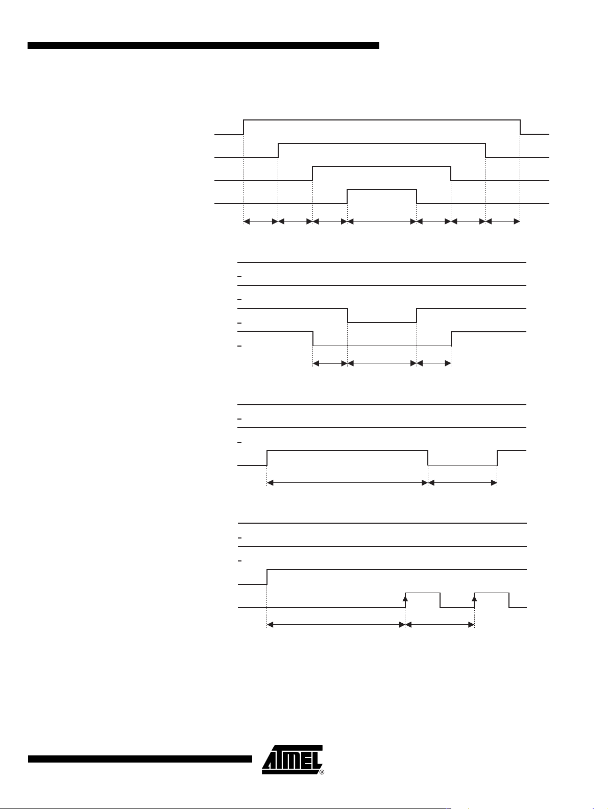
8. Timing
ATR0601 [Preliminary]
Figure 8-1. Recommended Power-up/down Sequence
VCC
VDIG
PUxto
PUrf
tmin = 0s
Figure 8-2. Recommended Sleep-mode Sequence
VCC
VDIG
PUxto
PUrf
tmin = 0s
tmin = 0s
tmin = 0s
tmin = 5ms
tmin = 4 µs
tmin = 0s tmin=0s tmin = 0s
tmin = 0s
Figure 8-3. Recommended XTO Start-up/Shut-down Sequence
VCC
VDIG
PUxto
tmin = 1 ms tmin = 4 µs
Figure 8-4. Sample Clock Start-up Delay
VCC
VDIG
PUxto
SC
tmax = 500 µs T = 1/23.104 MHz
4866A–GPS–08/05
7
Page 8

Figure 8-5. Synchronous Shut-down Behaviour of SC with Respect to PUxto
VCC
VDIG
PUxto
SC
T = 1/23.104 MHz
tmin = 0s
tmax = 25ns
tmax = 0s
Figure 8-6. Data Outputs SL and SH are Valid with Rising Edge of Sample Clock SC
SL
SH
SC
T = 1/23.104 MHz
8
ATR0601 [Preliminary]
4866A–GPS–08/05
Page 9

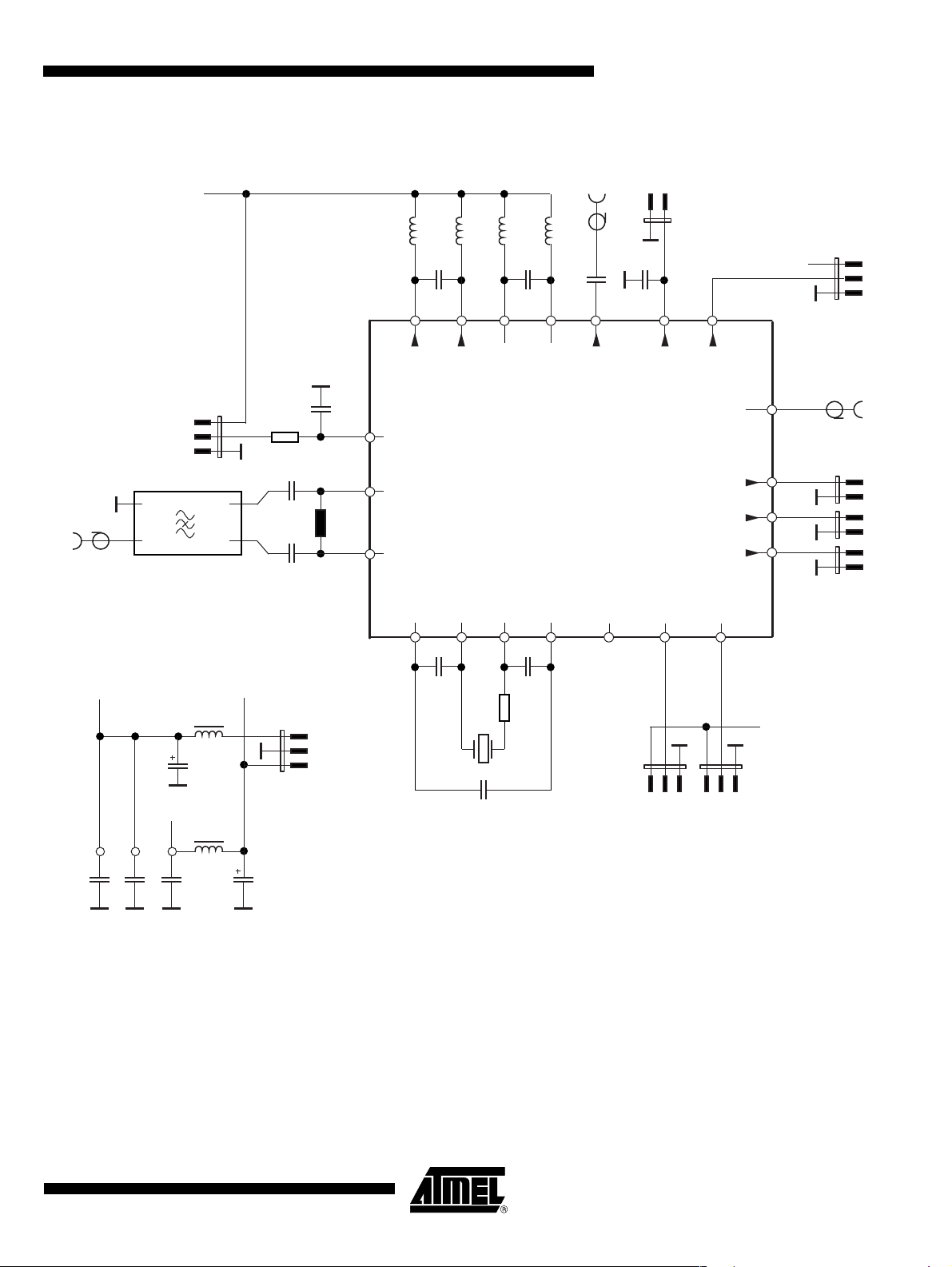
9. Application Circuit
ATR0601 [Preliminary]
Figure 9-1. Application Example Using a GPS Crystal with ESR
220nH
5pF
13
BP
220nH
14
NBP
VCO
PLL
XTO
VCC
220nH
15
BPI
5pF
220nH
16
NBPI
10nF
47pF
4.7nH
1.5pF
LNA section (opt.)
PU XTO
27
SAW
B4060
X1
PU RF
1.3pF
1.3pF
47pF
82pF
47pF
VCC
PU RF
ATR0610
Reference frequency: Application #1
17
18
11
5.6nH
10
6
3
5
4
100nF
100nF
100nF
PUxto
PUrf
RF
NRF
XTO
NXTO
X
NX
VDIG
VCC
VCC
7
19
1
VCC
VCC
VDIG
PMSS
Logic
GND
= 12Ω (Please see Table 9-1 on page 11)
typ
100pF
TEST
9
2
AGCO
NC12
MO8
20
EGC
SDI
1
A
D
A
D
SL
SH
SC
21
22
23
24
Data out "low"
Data out "high"
Sample clock
Note: Please consider the recommended IF-filter layout, shown in Figure 9-5 on page 11.
Figure 9-2. Application Example Using a GPS Crystal with ESR
≠ 12Ω
typ
(Please see Table 9-2 on page 11)
6
XTO
3
47pF
R1
82pF
X1
47pF
Reference frequency: Application #2
Note: The external series resistor R1 has to be selected depending on the typical value of the crystal
ESR. Please refer to Application Note “ATR0601: Crystal and TXCO selection”.
NXTO
5
X
4
NX
4866A–GPS–08/05
9
Page 10

Figure 9-3. Equivalent Application Examples Using a GPS TCXO (Please see Table 9-3 on
page 12)
TCXO
10 pF
22 pF
Do not
connect
Reference frequency: Application #4a
10 pF
TCXO
22 pF
Do not
connect
Reference frequency: Application #4b
33 pF
33 pF
6
XTO
3
NXTO
5
X
4
NX
6
XTO
3
NXTO
5
X
4
NX
Figure 9-4. Application Example Using an External Reference and Balanced Inputs
(Please see Table 9-4 on page 12)
1:1
Vin
Do not
connect
Reference frequency: Application #5
6
XTO
3
NXTO
5
X
4
NX
10
ATR0601 [Preliminary]
4866A–GPS–08/05
Page 11

ATR0601 [Preliminary]
Figure 9-5. Recommended IF-filter: Layout versus Schematic
13 14 15 16
Ca
Cb
Lc
Le Lf
A
BP
NBP
BPI
NBPI
13 14 15
Ld
B
Ca
Lc Ld Le
16
Cb
Lf
VCC
Note: Mutual inductance between the four inductors Lc - Lf plays an important role in the IF-filter charac-
teristics. In any design, the layout arrangement shown in Figure 9-5 on page 11 should be
resembled as close as possible. Measures: A = 2.8 mm; B = 1.4 mm; Lc - Lf: Wirewound SMD
inductors, 0603 size. (Please see Table 10-1).
Table 9-1. Specification of GPS Crystals Appropriate for the Application Example Shown in
Figure 9-1 on page 9
Parameter Comment Min. Typ. Max. Units
Frequency Characteristics
Fundamental Frequency
Calibration tolerance Frequency at 23°C ±2°C 7.0 ±ppm
Frequency deviation Over operating temperature range 15.0 ±ppm
Temperature range Operating temperature range –40.0 +85.0 °C
Electrical
Load capacitance (CL) 18.5 19.5 pF
Equivalent Series Resistance (ESR)
Fundamental Specification 7 12 23 Ω
Nominal frequency referenced to
25°C
23.104 MHz
4866A–GPS–08/05
Table 9-2. Specification of GPS Crystals Appropriate for the Application Example Shown in
Figure 9-2 on page 9
Parameter Comment Min. Typ. Max. Units
Equivalent Series Resistance (ESR)
Fundamental Specification 7 40 Ω
Note: All other parameters as specified in Table 9-1.
11
Page 12
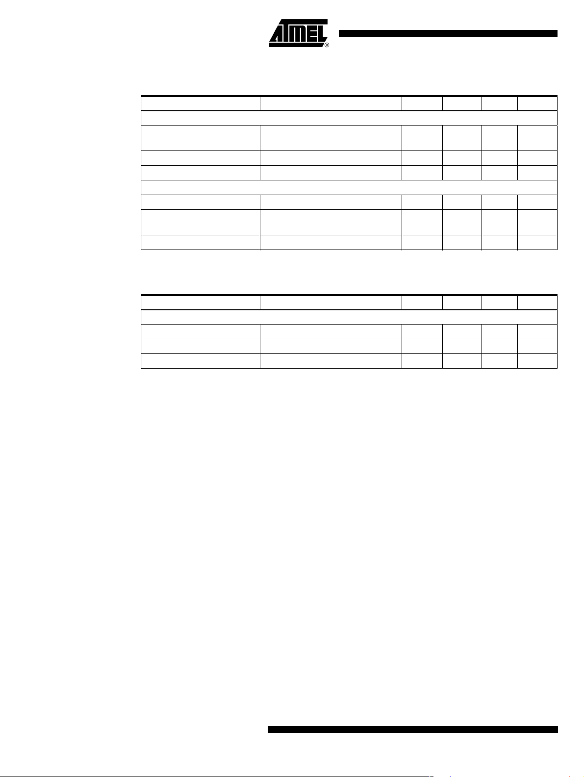
Table 9-3. Specification of GPS TCXOs Appropriate for the Application Example Shown in
Figure 9-3 on page 10
Parameter Comment Min. Typ. Max. Units
Frequency Characteristics
Nominal Frequency
Frequency deviation Over operating temperature range 2.0 ±ppm
Temperature range Operating temperature range –40.0 +85.0 °C
Electrical
Output waveform DC coupled clipped sinewave
Output voltage
(peak-to-peak)
Output load capacitance Tolerable load capacitance 10 pF
Nominal frequency referenced to
25°C
At minimum supply voltage 0.8 V
23.104 MHz
Table 9-4. Specification of an external reference signal for the application example shown in
Figure 9-4 on page 10
Parameter Comment Min. Typ. Max. Units
Signal Characteristics
Nominal Frequency 23.104 MHz
Waveform Sinewave or clipped sinewave
Amplitude Voltage peak-to-peak 0.6 0.8 1.0 V
12
ATR0601 [Preliminary]
4866A–GPS–08/05
Page 13
10. Demonstration Board
Figure 10-1. Schematic of Demonstration Board
V
CC
L3
13
L4
C21
14
L5 L6
C22 C3
15
ATR0601 [Preliminary]
P1
C10
816
J3
2
1
VDD1.8
20
2
1
2
3
P2
V
CC
V
V
CC
CC
19 17
C19 C8C9
NBP
BP
C17
C15
J1
C7
L2
11
10
9
TEST
RF
NRF
NXTO NX PURFXXTO
651718
X1
C4
J2
1
2
3
5
NIN
NOUT
6
IN
FI1
OUT
VDD1.8
FB1
C1
VDIG
FB2
R1
1
2
1
2
3
C2
NBPI
BPI MO
1243
C6C5
R7
NC
AGCO EGC
PUXTO
123123
SDI
SH
SL
SC
J9J8
21
23
22
24
VDD1.8
P4
1
J5
2
1
J6
2
1
J4
2
4866A–GPS–08/05
13
Page 14

Figure 10-2. Illustration of Demonstration Board
Table 10-1. BOM of Demonstration Board
Qty Value Device Parts Tolerance Manufacturer Mfr. Order Code
4 JP2E J3, J4, J5, J6 Molex 90120-0762
5 JP3E J1, J2, J7, J8, J9 Molex 90120-0763
1 0 RESISTOR-0402 R1 Vishay CRCW0402000Z
1 2n2 CAPACITOR-0402 C3 5% Vishay VJ0402Y222JXJA
2 1p3 CAPACITOR-0402 C15, C17 0,1 pF Tayo Yuden EVK105CH1R3BW
1
2 5p0 ±0p1 CAPACITOR-0402 C21, C22 ±0p1 Yageo America 0402CG509C9B200
2 10µ ELKO-B C1, C2 20% Vishay 293D106X0016B2
1 27 RESISTOR-0402 R7 5% Vishay CRCW040227RJ
2 47p CAPACITOR-0402 C5, C6 5% Vishay VJ0402A470JXXA.
1 82p CAPACITOR-0402 C4 Vishay VJ0402A820JXXA
4 100n CAPACITOR-0402 C7, C8, C9, C19 5% Vishay VJ0402V104JXJ
1 100p CAPACITOR-0402 C10 5% Vishay VJ0402A101JXXA.
3 142-0711-841 COAX-SMA P1, P2, P4 Johnson Comp. 142-0711-841
4 220n 2%
2 74279266 FERRITE_BEAD-0603 FB1, FB2
1 ATR0601-1 ATR0601-1 IC1 Atmel ATR0601
1 B4060 FILTER-BALANCED FI1 Epcos B4060
1
5n6 2%
Multilayer
RSX-5
23.104 MHz
INDUCTOR-0402 L2 2%
INDUCTOR_WIREWOUND-0603
XTAL-4PIN-6035 X1 Rakon
L3, L4, L5, L6 2%
Würth
Elektronik
Würth
Elektronik
Würth
Elektronik
744784056G
744761222G
74279266
XZC736 IEC19RSX-5
23.104 MHz
14
ATR0601 [Preliminary]
4866A–GPS–08/05
Page 15

11. Recommended Footprint
Figure 11-1. Recommended Footprint (QFN24 - 4 mm × 4 mm)
ATR0601 [Preliminary]
4866A–GPS–08/05
15
Page 16

12. Ordering Information
s
Extended Type Number Package Remarks
ATR0601-PFQW QFN24, 4 × 4 Taped and reeled
13. Package Information
Package: QFN 24 - 4 x 4
Exposed pad 2.6 x 2.6
(acc. JEDEC OUTLINE No. MO - 220)
Dimensions in mm
Not indicated tolerances ±0.05
24
1
6
Drawing-No.: 6.543-5101.02-4
Issue: 1; 03.06.05
0.9±0.1
+0
0.05-0.05
0.25
18
0.4
13
0.5 nom.
4
2.6
2.5
2419
1
technical drawing
according to DIN
6
712
specifications
16
ATR0601 [Preliminary]
4866A–GPS–08/05
Page 17

Atmel Corporation Atmel Operations
2325 Orchard Parkway
San Jose, CA 95131, USA
Tel: 1(408) 441-0311
Fax: 1(408) 487-2600
Regional Headquarters
Europe
Atmel Sarl
Route des Arsenaux 41
Case Postale 80
CH-1705 Fribourg
Switzerland
Tel: (41) 26-426-5555
Fax: (41) 26-426-5500
Asia
Room 1219
Chinachem Golden Plaza
77 Mody Road Tsimshatsui
East Kowloon
Hong Kong
Tel: (852) 2721-9778
Fax: (852) 2722-1369
Japan
9F, Tonetsu Shinkawa Bldg.
1-24-8 Shinkawa
Chuo-ku, Tokyo 104-0033
Japan
Tel: (81) 3-3523-3551
Fax: (81) 3-3523-7581
Memory
2325 Orchard Parkway
San Jose, CA 95131, USA
Tel: 1(408) 441-0311
Fax: 1(408) 436-4314
Microcontrollers
2325 Orchard Parkway
San Jose, CA 95131, USA
Tel: 1(408) 441-0311
Fax: 1(408) 436-4314
La Chantrerie
BP 70602
44306 Nantes Cedex 3, France
Tel: (33) 2-40-18-18-18
Fax: (33) 2-40-18-19-60
ASIC/ASSP/Smart Cards
Zone Industrielle
13106 Rousset Cedex, France
Tel: (33) 4-42-53-60-00
Fax: (33) 4-42-53-60-01
1150 East Cheyenne Mtn. Blvd.
Colorado Springs, CO 80906, USA
Tel: 1(719) 576-3300
Fax: 1(719) 540-1759
Scottish Enterprise Technology Park
Maxwell Building
East Kilbride G75 0QR, Scotland
Tel: (44) 1355-803-000
Fax: (44) 1355-242-743
RF/Automotive
Theresienstrasse 2
Postfach 3535
74025 Heilbronn, Germany
Tel: (49) 71-31-67-0
Fax: (49) 71-31-67-2340
1150 East Cheyenne Mtn. Blvd.
Colorado Springs, CO 80906, USA
Tel: 1(719) 576-3300
Fax: 1(719) 540-1759
Biometrics/Imaging/Hi-Rel MPU/
High Speed Converters/RF Datacom
Avenue de Rochepleine
BP 123
38521 Saint-Egreve Cedex, France
Tel: (33) 4-76-58-30-00
Fax: (33) 4-76-58-34-80
Literature Requests
www.atmel.com/literature
Disclaimer: The information in this document is provided in connection with Atmel products. No license, express or implied, by estoppel or otherwise, to any
intellectual property right is granted by this document or in connection with the sale of Atmel products. EXCEPT AS SET FORTH IN ATMEL’S TERMS AND CONDI-
TIONS OF SALE LOCATED ON ATMEL’S WEB SITE, ATMEL ASSUMES NO LIABILITY WHATSOEVER AND DISCLAIMS ANY EXPRESS, IMPLIED OR STATUTORY
WARRANTY RELATING TO ITS PRODUCTS INCLUDING, BUT NOT LIMITED TO, THE IMPLIED WARRANTY OF MERCHANTABILITY, FITNESS FOR A PARTICULAR
PURPOSE, OR NON-INFRINGEMENT. IN NO EVENT SHALL ATMEL BE LIABLE FOR ANY DIRECT, INDIRECT, CONSEQUENTIAL, PUNITIVE, SPECIAL OR INCIDENTAL DAMAGES (INCLUDING, WITHOUT LIMITATION, DAMAGES FOR LOSS OF PROFITS, BUSINESS INTERRUPTION, OR LOSS OF INFORMATION) ARISING OUT
OF THE USE OR INABILITY TO USE THIS DOCUMENT, EVEN IF ATMEL HAS BEEN ADVISED OF THE POSSIBILITY OF SUCH DAMAGES. Atmel makes no
representations or warranties with respect to the accuracy or completeness of the contents of this document and reserves the right to make changes to specifications
and product descriptions at any time without notice. Atmel does not make any commitment to update the information contained herein. Unless specifically provided
otherwise, Atmel products are not suitable for, and shall not be used in, automotive applications. Atmel’s products are not intended, authorized, or warranted for use
as components in applications intended to support or sustain life.
© Atmel Corporation 2005. All rights reserved. Atmel®, logo and combinations thereof, Everywhere You Are® and others, are registered trade-
marks or trademarks of Atmel Corporation or its subsidiaries. Other terms and product names may be trademarks of others.
Printed on recycled paper.
4866A–GPS–08/05
 Loading...