

Page 1
Features
• Very Low Power Design (≈ 50 mW)
• Single IF Concept
• 2-bit ADC on Chip
• Small QFN Package (28 Pins)
• Highly Integrated, Few External Components
• UHF6 Technology
GPS
Electrostatic sensitive device.
Observe precautions for handling.
Description
With the growing importance of mobile communication, location awareness is a key
feature for more and more products and services. Due to its small size and minimal
power consumption, the GPS front-end IC ATR0600 is an ideal solution for mobile
applications and navigation systems.
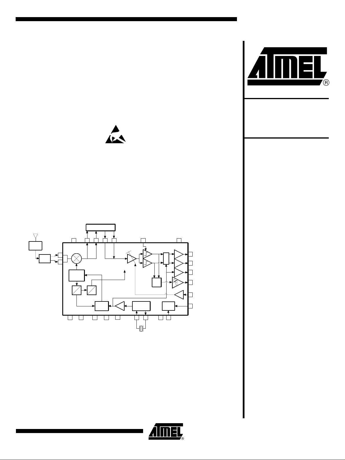
Figure 1. Block Diagram
1575.42 MHz
Ant
LNA
SAW
RFIN
RFNIN
VS3
VCO
1478.6
MHz
64
96.76 MHz
LC-BP
NBPI
BPI
BP
NBP
VGA amp
BP-Filter
1
1
4
PFD XTO
REF
OR
Power
control
VDIG
Dig. IF at 4.35 MHz
SIGH
SIGL
SC
23.104 MHz
AGCO
GC
P2
Front-end IC
ATR0600
Preliminary
VS1
VS2
VS5
VS7
X
XTO
23.104 MHz
NXTO
NX
P1
Rev. 4536F–GPS–10/03
Page 2
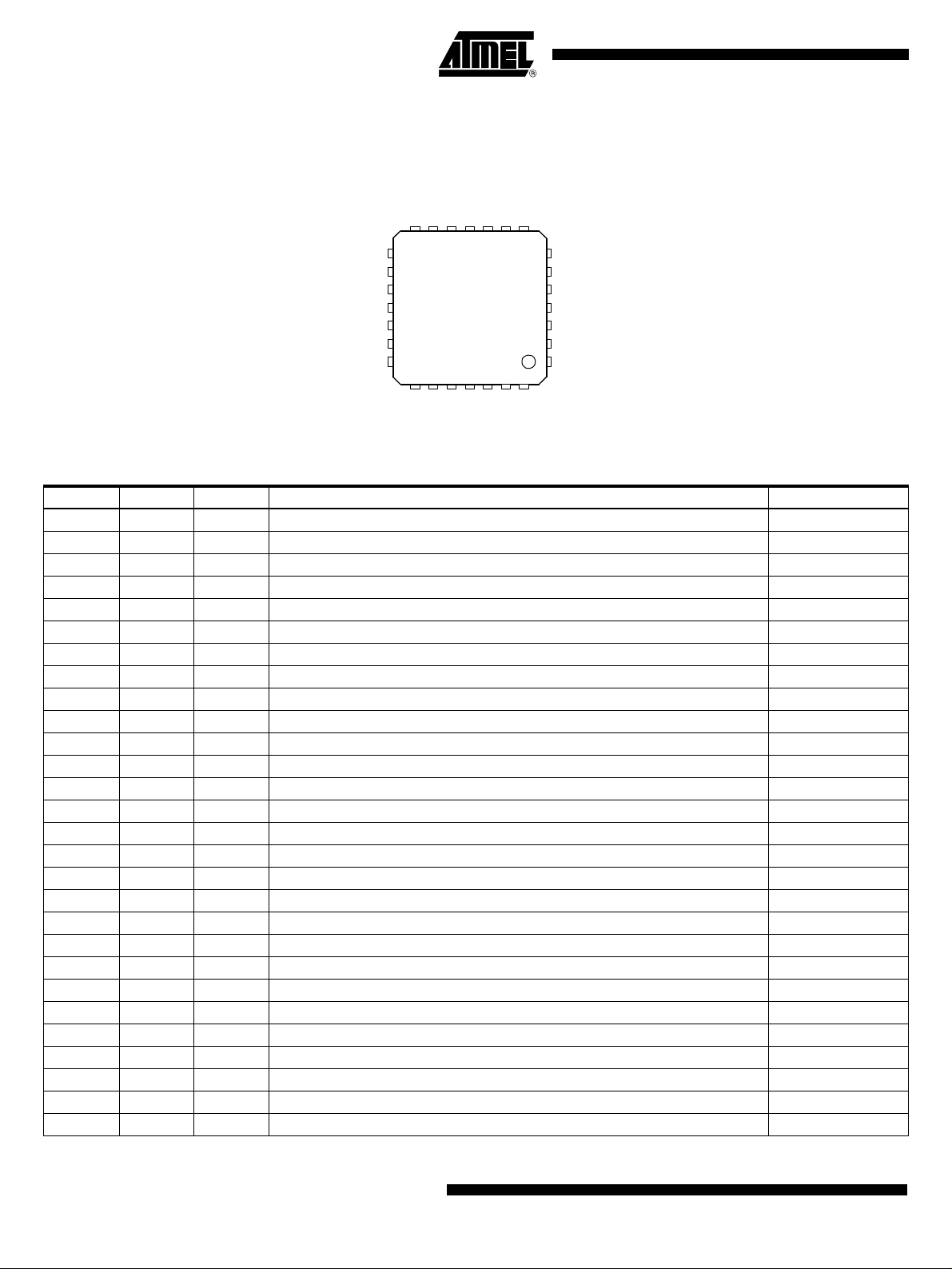
Pin Configuration
Figure 2. Pinning QFN28
N
I
N
.
N
I
BP
NBP
BPI
NBPI
VS1
n.c.
n.c.
c
.
n
14 13 12 11 10 9 8
15
16
17
18
19
20
21
22 23 24 25 26 27 28
C
G
3
F
F
S
R
R
V
L
F
2
E
S
G
I
V
R
S
.
c
1
2
.
P
P
n
7
X
6
VS5
5
XTO
4
NXTO
3
VS7
2
NX
1
AGCO
H
C
G
I
S
G
I
D
S
V
Pin Description
Pin Symbol Type Function Protection Level
1 AGCO O Signal level output ESD3
2 NX OB Complementary to X ESD3
3 VS7 P ECL - blocks supply ESD2
4 NXTO IB Complementary to XTO ESD3
5 XTO IB Quartz input ESD3
6 VS5 P XTO supply ESD2
7 X OB Quartz intermediate output ESD3
8 n.c. – Not connected –
9 P2 I Power-up quartz oscillator ESD3
10 P1 I Power-up RF part ESD3
11 VS3 P Reference supply ESD2
12 RFIN IB RF input 1.575 GHz ESD3
13 RFNIN IB Complementary to RFIN ESD3
14 n.c. – Not connected –
15 BP IB Open-collector output of mixer ESD3
16 NBP IB Complementary to BP ESD3
17 BPI IB IF - filter input ESD3
18 NBPI IB Complementary to BPI ESD3
19 VS1 P VCO + mixer + VGA supply ESD2
20 n.c. – Not connected –
21 n.c. – Not connected –
22 GC I Gain control input ESD3
23 VS2 P Subsampling unit supply ESD2
24 REF O Defining low threshold voltage ESD3
25 SIGL O Digital interface subsampled output high threshold voltage refered to REF1 ESD3
26 SIGH O Digital interface subsampled output low threshold voltage refered to REF2 ESD3
27 VDIG P Digital interface supply voltage 1.8 V ESD2
28 SC O Digital interface clock output ESD3
2
ATR0600 [Preliminary]
4536F–GPS–10/03
Page 3

ATR0600 [Preliminary]
Functional
Description
The specification of GPS receivers for personal mobile applications strongly differs from
stand-alone GPS receiver specifications. One reason is the presence of strong blocking
signals from mobile transmitters which might cause unacceptable levels of degradation
in the carrier-to-noise ratio of a GPS system if not sufficiently suppressed. The other
reason is the requirements for very low power consumption.
The ATR0600 GPS receiver IC has been especially designed for GPS applications in
mobile phones. From this system point of view, it incorporates highest isolation between
GPS and cellular antennas, as well as low power consumption. The ATR0600 contains
a low-power single IF design and integrates a complete frequency synthesizer. It is fully
functional over a supply-voltage range of 2.7 V to 3.3 V and is housed in a 28-pin
QLN package.
The GPS receiver's input signal is a Direct Sequence Spread Spectrum (DSSS) signal
at 1575.42 MHz with a 1.023 Mbps Bi-Phase-Shift-Keying (BPSK) modulated spreading
code. As the input signal power at the antenna is approximately -140 dBm, the desired
signal is below the thermal noise floor.
LNA/Mixer Stage The ATR0600 receives the L1 GPS signal via an external LNA. The LNA bandwidth
should be as narrow as possible to avoid interferences from out-of-band signals (especially from those of the 1800 GSM band).
Combined with the antenna the LNA provides a first filtering of the GPS signal. The LNA
in addition should have a power shutdown feature. The shutdown signal will be generated inside the digital section of the GPS receiver. The output of the LNA drives an
external SAW filter, which provides the image rejection for the mixer and the isolation of
the 1800-MHz GSM band. The output of the SAW filter drives a highly linear mixer which
down-converts the GPS signal to an IF of 97.76 MHz.
IF Stage The mixer directly drives an external LC-bandpath filter. In order to provide the ultimate
selectivity of the GPS frequency before the A/D conversion of the receiver part, the
signal path of the ATR0600 combines an external filter and a second integrated filter.
We recommend to design the external filter as a 2-pole filter with quality factor Q > 25.
VGA Amplifier Stage The output of the LC-filter drives an on-chip Variable Gain-Controlled amplifier (VGA)
which is combined with an integrated IF-bandpath filter to perform additional filtering of
GSM jamming signals. The AGC stage provides the additional gain needed to optimally
load the signal range of the following analog/digital converter. The AGC control loop can
be selected either on-chip close loop or open loop mode. Connecting the AGC_OUT
output directly to the AGC_CNTRL input activates the internal control loop.
In that case, the VGA control signal is passed to the VGA via an integrated buffer stage
including all necessary filtering (low-pass filter). The external control loop is closed by
the baseband IC ATR0620.
A/D Converter Stage The output of the VGA drives the integrated 1.5-bit analog-to-digital converter stage,
which comprises two comparators and two output drivers in order to provide sign and
magnitude output bits to the baseband IC ATR0620. The comparator LOW- and HIGHthresholds (in Figure 1 on page 1 for SIGH and SIGL) are adjustable via external resistor. The OR gate closes the internal AGC control loop.
Power Save Setting
Stage
The integrated power-control stage is controlled by the baseband IC ATR0620 via P1
and P2. The input signals control the shutdown of the reference crystal oscillator (P2) or
the shutdown of the whole RF section (P1).
4536F–GPS–10/03
3
Page 4
.
Absolute Maximum Ratings
Stresses beyond those listed under “Absolute Maximum Ratings” may cause permanent damage to the device. This is a stress rating
only and functional operation of the device at these or any other conditions beyond those indicated in the operational sections of this
specification is not implied. Exposure to absolute maximum rating conditions for extended periods may affect device reliability.
Parameters Symbol Value Unit
Supply voltage V
Input voltage V
Junction temperature T
Storage temperature range T
S
in
j
stg
3.7 V
3.7 V
125 °C
-40 to +125 °C
Thermal Resistance
Parameters Symbol Value Unit
Junction ambient R
thJA
125 K/W
Recommended Operating Conditions
Parameters Symbol Value Unit
Supply voltage V
S
Temperature range Temp -40 to +85 °C
Input frequency f
Reference frequency f
in, mixer
ref
External IF filter (see Figure 13 on page 9)
Supply voltage digital interface, pin 27 V
DD
2.7 to 3.3 V
1575.42 MHz
23.104 MHz
1.65 to 2.0 V
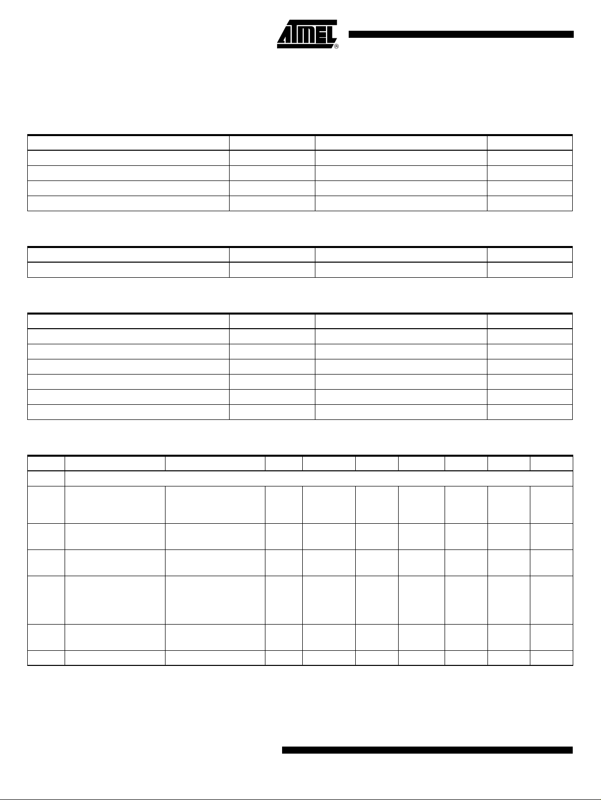
Electrical Characteristics
No. Parameters Test Conditions Pin Symbol Min. Typ. Max. Unit Type*
1Common
3, 6,
1.1 Supply current P1 = P2 = VPU
on
11,
19, 23
1.2 Supply current XTO
1.3
Supply current digital
interface
P1 = VPU
P2 = VPU
P1 = P2 = VPU
off
on
on
6I
27 I
3, 6,
1.4
Supply current (power
down)
P1 = P2 = VPU
OFF
11,
19,
23, 27
1.5 Total gain
RFIN, RNIN matched,
to 50 W, V
= 2.2 V
GC
1 G 95 dB B
1.6 Noise figure N
*) Type means: A = 100% tested, B = 100% correlation tested, C = Characterized on samples, D = Design parameter
XTO
I
S, pd
I
DD
S
18 mA A
2mAA
250 µA A
20 µA A
F
6.9 dB C
4
ATR0600 [Preliminary]
4536F–GPS–10/03
Page 5

ATR0600 [Preliminary]
Electrical Characteristics (Continued)
No. Parameters Test Conditions Pin Symbol Min. Typ. Max. Unit Type*
2 Mixer and 1st IF-filter
2.1 Output frequency f
2.2 Input impedance f
nd
3VGA and 2
3.1
Bandpass center
frequency
IF-filter
3.2 Minimum gain VGC = 1.0 V G
3.3 Maximum gain V
3.4
3.5
3.6
Control-voltage
sensitivity
Gain-control output
cut-off frequency
Gain-control output
voltage
= 23.104 MHz 15, 16 f
ref
= 1575 MHz 12, 13 Z
ref
= 23.104 MHz f
f
ref
= 2.2 V G
GC
= 2.2 V
V
GC
V
= 1.0 V
GC
N
Without external load F
at 50 pF load 1 V
IF
in, IF
in, VGA
VGA, m in
VGA, max
N
vga, min
vga, max
agc_out
agc_out
1.0 2.2 V B
4 Reference Oscillator
4.1
4.2
XTO phase noise
at 100 Hz
XTO phase noise
at 1 kHz
28 P
28 P
n100
n1k
5 Clock and Data Driver
5.1
5.2 Clock output level C
5.3 Clock output level C
5.4 Data output level C
5.5 Data output level C
Clock driver
frequency
28 f
= 10 pF 28 V
load
= 10 pF 28 V
load
= 10 pF 25, 26 V
load
= 10 pF 25, 26 V
load
clk
clkhigh
clklow
datahigh
datalow
6 Power-up, Pins P1 and P2
6.1
6.2
Power-on voltage
level on
Power-on voltage
level off
9, 10 VPU
9, 10 VPU
6.3 Power-on delay time 9, 10 TPU
on
off
on, off
0.9 V C
*) Type means: A = 100% tested, B = 100% correlation tested, C = Characterized on samples, D = Design parameter
96.76 MHz B
13 - j80 W C
96.76 MHz
0dBD
75 dB D
6.6
150
dB/V
dB/V
100 kHz D
-80 dBc/Hz C
-100 dBc/Hz C
23.104 MHz A
0.8 ´
V
DD
0.2 ´
V
DD
0.8 ´
V
DD
0.2 ´
V
DD
VB, C
VC
VC
VC
0.3 V C
6µsC
D
D
4536F–GPS–10/03
5
Page 6

Interface Description Figure 3. Clock Interface
V
G
VDIG
20k
SC
SC
Figure 4. SIGH Interface
Figure 5. SIGL Interface
Chip
VDIG
Chip
DIG
Chip
I
Maximum load capacitance
20k
SIGH
I
20k
SIGL
I
10p
SIGH
10p
Maximum load cap.
SIGL
10p
Maximum load cap.
Figure 6. Supply VDIGI Interface
VDIG
Chip
VDI
1.8V
Supply
Figure 7. Power Control Interface P1
20k
50k
100k
Chip
6
ATR0600 [Preliminary]
P1
VDD
P1
Application
4536F–GPS–10/03
Page 7

Figure 8. Power Control Interface P2
CC
ATR0600 [Preliminary]
20k
P2
50k
100k
Chip
P2
Application
Figure 9. Automatic Gain-control Interface
32uA
Chip
44k
I
150k
AGCO
50p
AGCO
GC
100p
Chip, connected to AGCO
Figure 10. A/D Reference Level-control Interface Ref
VCC
I
Ref
Ref
VDD
V
Chip
Application
Select value on test
R optional
4536F–GPS–10/03
7
Page 8

Figure 11. Mixer Input Interface
2mA
2.5k
Chip
250uA
2.5k
VCC
RF
NRF
Figure 12. XTO Interface
NRF
XTO
X
RF
Application (Matching)
100k
220
XTO
47p
Chip
47p
220
RFx
NRFx
NXTO
NX
NXTO
X
8
ATR0600 [Preliminary]
68p
Application
NX
4536F–GPS–10/03
Page 9

Figure 13. IF-filter Interface
VCC
Imax
2mA
ATR0600 [Preliminary]
BP
BP
2p
300fF
BPI
BPI
220nH
220nH
Figure 14. Mixer Input Impedance at RF-NRF
60uA
60uA
VCC
Imax
2mA
Chip
2p
5p
5p
NBPI
NBPI
2p
300fF
NBP
NBP
2p
Application (IF-Filter)
220nH
220nH
VCC
68
4536F–GPS–10/03
9
Page 10

Ordering Information
Extended Type Number Package Remarks
ATR0600-PJQ QFN28 - 5x5 Taped and reeled
Package Information
10
ATR0600 [Preliminary]
4536F–GPS–10/03
Page 11

Atmel Corporation Atmel Operations
2325 Orchard Parkway
San Jose, CA 95131, USA
Tel: 1(408) 441-0311
Fax: 1(408) 487-2600
Regional Headquarters
Europe
Atmel Sarl
Route des Arsenaux 41
Case Postale 80
CH-1705 Fribourg
Switzerland
Tel: (41) 26-426-5555
Fax: (41) 26-426-5500
Asia
Room 1219
Chinachem Golden Plaza
77 Mody Road Tsimshatsui
East Kowloon
Hong Kong
Tel: (852) 2721-9778
Fax: (852) 2722-1369
Japan
9F, Tonetsu Shinkawa Bldg.
1-24-8 Shinkawa
Chuo-ku, Tokyo 104-0033
Japan
Tel: (81) 3-3523-3551
Fax: (81) 3-3523-7581
Memory
2325 Orchard Parkway
San Jose, CA 95131, USA
Tel: 1(408) 441-0311
Fax: 1(408) 436-4314
Microcontrollers
2325 Orchard Parkway
San Jose, CA 95131, USA
Tel: 1(408) 441-0311
Fax: 1(408) 436-4314
La Chantrerie
BP 70602
44306 Nantes Cedex 3, France
Tel: (33) 2-40-18-18-18
Fax: (33) 2-40-18-19-60
ASIC/ASSP/Smart Cards
Zone Industrielle
13106 Rousset Cedex, France
Tel: (33) 4-42-53-60-00
Fax: (33) 4-42-53-60-01
1150 East Cheyenne Mtn. Blvd.
Colorado Springs, CO 80906, USA
Tel: 1(719) 576-3300
Fax: 1(719) 540-1759
Scottish Enterprise Technology Park
Maxwell Building
East Kilbride G75 0QR, Scotland
Tel: (44) 1355-803-000
Fax: (44) 1355-242-743
RF/Automotive
Theresienstrasse 2
Postfach 3535
74025 Heilbronn, Germany
Tel: (49) 71-31-67-0
Fax: (49) 71-31-67-2340
1150 East Cheyenne Mtn. Blvd.
Colorado Springs, CO 80906, USA
Tel: 1(719) 576-3300
Fax: 1(719) 540-1759
Biometrics/Imaging/Hi-Rel MPU/
High Speed Converters/RF Datacom
Avenue de Rochepleine
BP 123
38521 Saint-Egreve Cedex, France
Tel: (33) 4-76-58-30-00
Fax: (33) 4-76-58-34-80
Literature Requests
www.atmel.com/literature
Disclaimer: Atmel Corporation makes no warranty for the use of its products, other than those expressly contained in the Company’s standard
warranty which is detailed in Atmel’s Terms and Conditions located on the Company’s web site. The Company assumes no responsibility for any
errors which may appear in this document, reserves the right to change devices or specifications detailed herein at any time without notice, and
does not make any commitment to update the information contained herein. No licenses to patents or other intellectual property of Atmel are
granted by the Company in connection with the sale of Atmel products, expressly or by implication. Atmel’s products are not authorized for use
as critical components in life support devices or systems.
© Atmel Corporation 2003. All rights reserved.
®
and combinations thereof are the registered trademarks of Atmel Corporation or its subsidiaries.
Atmel
Other terms and product names may be the trademarks of others.
Printed on recycled paper.
4536F–GPS–10/03
 Loading...