

Page 1

Main Features
• High Sensitivity and High SNR Performance 1/2" CMOS Sensor
• Total Resolution of 1.3M (with 5 µm Square Pixels)
• High Data Rate: 75 Mpixels/s Provides 60 Frame/s at 1M Resolution (for 1M60)
• CameraLink
• Flexible and Easy to Operate via Serial Communication Control
– Gain: 0 dB to 18 dB in 3 dB Steps
– Dynamic Range: 8, 10 or 12-bit Data
– Contrast Expansion
– Shutter Time Pogrammable
– Subsampling: 1/4 and 1/16 Resolution
– Trigger Mode: Free-run or External Trigger Mode
– Programmable ROI
– Test Pattern
• Column FPN Correction
• Programmable Look-up Table
• Single Power Supply: DC 12 V to 24 V Provided on Hirose-6 Connector
• Input TTL Trigger Signal and Output TTL Shutter Signal on Hirose-5 Connector
• Compact Design: 44 × 44 × 45 mm (w, h, l)
• C-mount Adapter
• High Reliability - CE and FCC Compliant
®
Data Format (Base Configuration - 1 Channel)
CameraLink®
Areascan
Cameras
™
ATMOS
ATMOS
1M60
™
1M30
Product Description
This camera features an outstanding sensitivity and SNR, even at maximal speeds.
The ROI allows to increase the frame rate (for instance, 175 fps in VGA format 1M60).
ATMOS™ cameras are based on a rolling shutter CMOS sensor.
The configuration interface provides access to advanced functions (contrast expansion, image calibration, LUT). The versatile and compact mechanical housing enables
you to implement various configurations.
These features combined with a compelling price, make ATMOS
tive for users of megapixel cameras.
an attractive alterna-
Applications
High-speed, SNR performance and reliability of this camera make it suitable for
machine vision, especially:
Material Inspection (e.g. glass, IC, PCB)
•
• Robot Guidance
• Metrology
and various applications like:
•
Microscopy
• Surveillance Demanding Tasks
Preliminary
5429B–IMAGE–04/05
Page 2

1. Typical Performances
Table 1-1. Camera Typical Performances
Sensor Characteristics at Maximum Pixel Rate
1M60 1M30 Unit
Resolution H × V 1312 × 1024 1312 × 1024 Pixels
Pixel size (square) 5 × 5 5 × 5 µm
Maximum frame rate 48 24 Hz
Pixel rate 75 37.5 MHz
Camera Performances
Bit depth 8, 10 or 12 Bits
Spectral range 350–1000 nm
Linearity ±2% in 5% and 95% of FSR
PRNU 1.5% rms
FPN 0.1% rms
Responsivity 10000
(1)
LSB/(Lux.s)
Output RMS Noise
Dynamic range
Conversion factor 10 e-/ LSB
Dark Current 1500 e-/s
Over Illumination Behavior 75 Esat
Mechanical and Electrical Interface
Size (w × h × l) 44 × 44 × 45 mm
Weight 115 g
Lens Mount C-mount
Sensor Alignment
Power supply single 12 to 24 VDC
Power consumption < 2 W
Operating temperature 0 to 55 (non-condensing) °C
Storage temperature -40 to 70 (non-condensing) °C
< 2.7 LSB rms
> 63
(2)
∆x, y = ± 250
∆z = ±150
= ± 0.7
∆0
xy
= 0-200
∆tilt
z
dB
µm
µm
degree
µm
Measured with light source 3200°K and IR filter
Warning:
1. When exposed to such illumination level the sensor might lock-up and should be reset
2
See Register Software Reset @ 206H, Internal Register Mapping on page 17
ATMOS -1M60/1M30 [Preliminary]
5429B–IMAGE–04/05
Page 3
[Preliminary] ATMOS -1M60/1M30
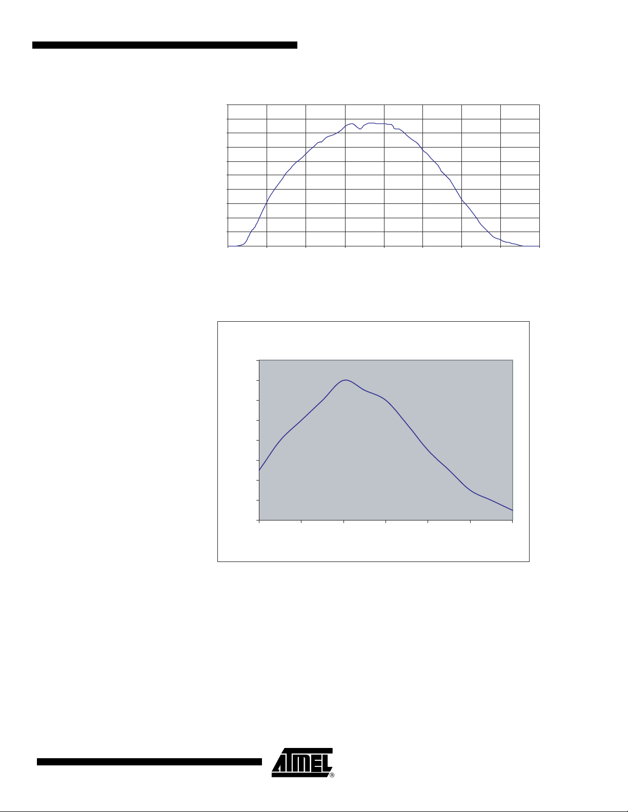
Figure 1-1. Responsivity Diagram
50
45
40
35
)
2
30
25
20
LSB/( nJ/cm
15
10
5
0
300 400 500 600 700 800 900 1000 1100
Figure 1-2. Quantum Efficiency
Responsivity at 0 dB Gain
nm
Quantum Efficiency
0,8
0,7
0,6
0,5
0,4
QE (%)
0,3
0,2
0,1
0
400 500 600 700 800 900 1000
Wavelength (nm)
5429B–IMAGE–04/05
3
Page 4

2. Standard Conformity
The cameras have been tested in the following conditions:
• Camera with complete Atmel housing
• Shielded power supply cable
• CameraLink data transfer cable ref. 14B26-SZLB-500-OLC (3M™)
• Linear AC-DC power supply
Atmel recommends using the same configuration to ensure compliance with the following
standards.
2.1 CE Conformity
The ATMOS cameras comply with the European directive 89/336/CEE (EN55022 A/CISPR22 A,
EN55024, EN61000-6-2).
2.2 FCC conformity
ATMOS Cameras comply with Part 15 of FCC rules. Operation is subject to the following two
conditions:
1. This device may not cause harmful interference, and
2. This device must accept any interference received, including interference that may
cause undesired operation.
This equipment has been tested and found to comply with the limits for a Class A digital device,
pursuant to part 15 of the FCC Rules. These limits are designed to provide reasonable protection against harmful interference when the equipment is operated in a commercial environment.
This equipment generates, uses, and can radiate radio frequency energy and, if not installed
and used in accordance with the instruction manual, may cause harmful interference to radio
communications. Operation of this equipment in a residential area is likely to cause harmful
interference in which case the user will be required to correct the interference at his own
expense.
Warning: Changes or modifications to this unit not expressly approved by the party responsible
for compliance could void the user's authority to operate this equipment.
4
ATMOS -1M60/1M30 [Preliminary]
5429B–IMAGE–04/05
Page 5
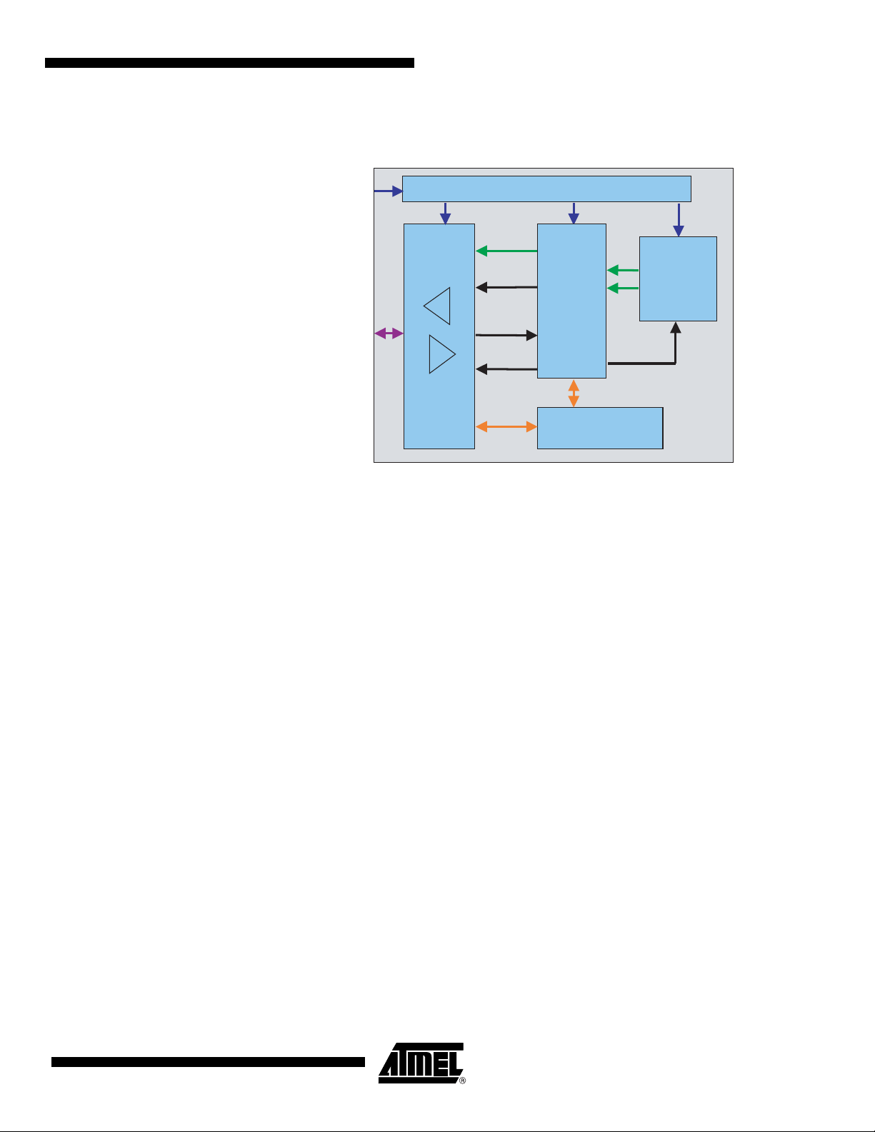
3. Camera Description
Figure 3-1. Camera Synoptic
[Preliminary] ATMOS -1M60/1M30
DC power
Camera Link
I/F
CameraLink
Transceiver
TX
RX
Power Supplies
Data
Strobe, LVAL
FVAL
Trigger
Shutter
Serial Line
Sequencer
Controller
Microcontroller
CMOS
SENSOR
The camera is based on a single tap CMOS sensor which delivers a 12-bit digital video signal at
its output. An FPGA has been implemented for image processing (FPN column correction, conversion LUT, contrast expansion). The camera is powered by a single DC power supply from
12V to 24V. The functional interface (data and control) is provided with the CameraLink interface. The camera uses the base configuration of the CameraLink standard.
Note: DVAL permanently tied to 1 (high) level.
Data can be delivered on a single channel or two de-multiplexed channels. The data format configuration might be in 12-bit, 10-bit, or 8-bit. It is possible to use external triggers with the camera
(CC1 signal or TTL_IO trigger input) in different trigger modes see ”Synchronization Modes” on
page 6 The camera configuration and settings are done via the CameraLink serial communica-
tion. This interface is used for:
5429B–IMAGE–04/05
• Gain and offset setting
• Data output format
• Synchronization modes: free-run or external trigger modes
• Shutter time
• Test pattern generation
• Upload and download of correction data (FPN column correction, LUT)
5
Page 6

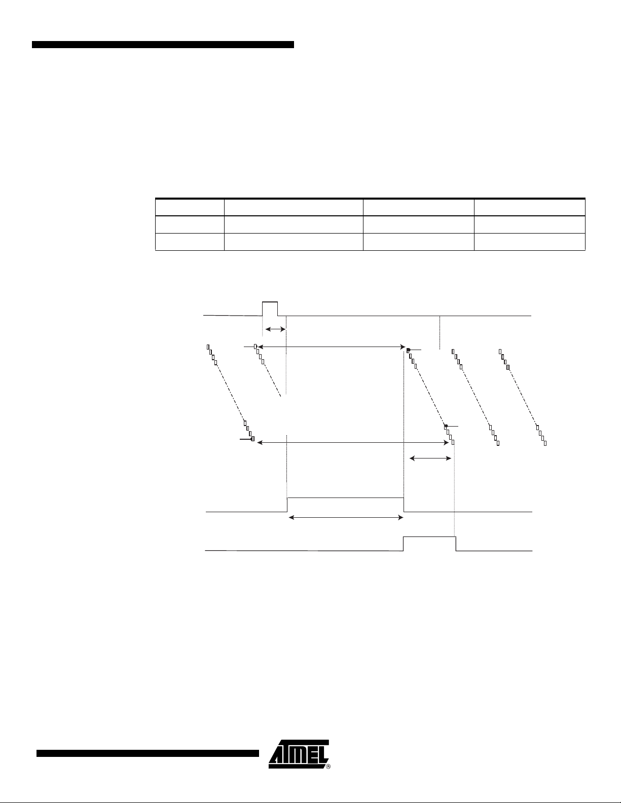
4. Timing
4.1 Synchronization Modes
The camera operates in rolling shutter mode.
4.1.1 Optimal Use of the Rolling Shutter
As shown in the following timing diagrams, Figure 4-1, exposure does not happen at the same
time for all lines, which can lead to image distortion when capturing fast moving objects. The
way to bypass this, is to use the camera with a strobe light or a shutter element so that all the
lines are exposed during the same time and no image distortion is visible when capturing fast
moving objects.
The integration time for each line is: readout (+ programmable shutter time, when used). A shutter signal is provided to strobe a light source or to drive a shutter element. You can set the
camera to operate in one of the following synchronization modes: periodic, triggered, triggered
without full reset and ITC. See register Mode Control @ 204H, Internal Register Mapping on
page 17.
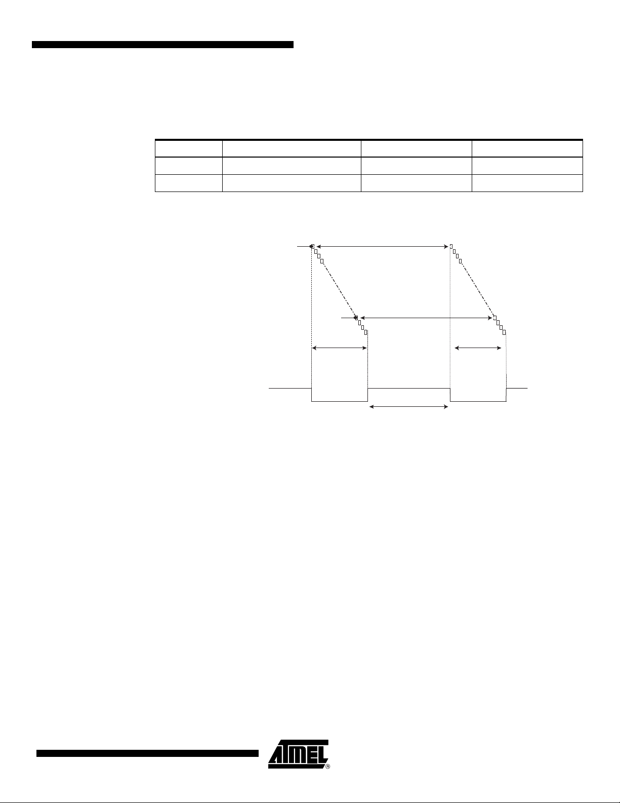
4.1.2 Free-run Mode (or Periodic Mode) Principle: The camera operates in periodic mode.
The period is defined by readout time (+ programmable shutter time, when used). Valid data is
forwarded to the CameraLink interface during the next frame readout starting with the first line.
If shutter time is set to 0:
The frame N is readout while the first line integrates for frame N+1. As soon as the frame N
readout has ended starts the readout of frame N +1.
Figure 4-1. Free-run Mode Chronogram
Line 1
Integration
Line 1 Readout
and Reset
Line n Readout
and Reset
(frame N)
Line n
Integration
(Frame N)
Frame N
Readout
Frame N+1
Readout
6
ATMOS -1M60/1M30 [Preliminary]
5429B–IMAGE–04/05
Page 7
[Preliminary] ATMOS -1M60/1M30
)
t
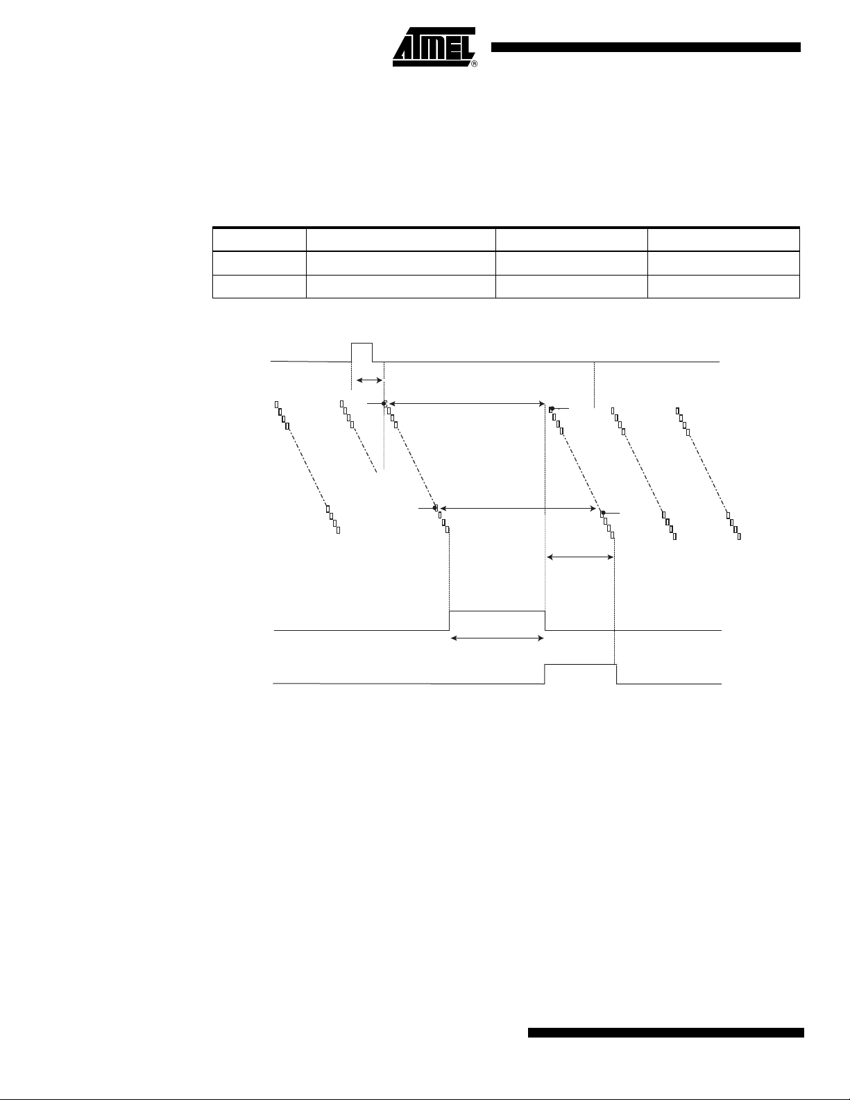
If shutter time is set to > 0:
Readout is suspended between two consecutive frame readout and shutter output signal is activated (programmable polarity) for a time configurable within 0 to Tsh range by step of T1.
Table 4-1. Shutter Time Values at Free-run Mode
Label Description 1M60 1M30
Tsh Maximum shutter time (ms) 655 1310
T1 Step duration (µs) 10 20
Figure 4-2. Free-run Mode and Shutter Chronogram
Line 1
Integration
Line 1
Line n Readout
and Reset
Readout
and Rese
(Frame N
Line n
Integration
(Frame N)
4.1.3 Triggered Mode
Shutter
Frame N - 1
Readout
out
Time
Programmable
Shutter Time
Frame N
Readout Time
The maximum frame rate of 48 frame/s for the 1M60 camera (or 24 frame/s for the 1M30 camera) is given in this mode with a shutter time set to 0.
See register Aperture Shutter Time @ 246H, Internal Register Mapping on page 17.
Principle: An external trigger starts the reset of the sensor, then snap and readout of a frame,
the integration time is defined by readout time (+ programmable shutter time, when used).
The trigger event initiates the following sequence:
• Stop of readout frame in progress and reset of readout pointer to line 1
• Readout of previous dummy frame and integration start of the frame N. The readout data of
previous frame is not forwarded on CameraLink interface (FVAL inactive)
• Shutter output signal is activated during a time programmable within 0 to Tsh range by step
of T1
• Readout of frame N. The readout data is forwarded to the CameraLink interface (FVAL
active) starting with the first line
• Readout of dummy frames (to prevent against large dark current integration) while the
camera waits for the next trigger event
5429B–IMAGE–04/05
7
Page 8
The trigger delay is a few µs. The minimum pulse duration is 1µs. The edge of trigger is programmable. The source of trigger is selectable between CameraLink CC1 signal and TTL/IO
trigger input. The period is defined by readout time + programmable shutter time + readout time
+ wait. Therefore the minimum period is 2
× readout time.
See register Aperture Shutter Time @ 246H, Internal Register Mapping on page 17.
Table 4-2. Shutter Time Values at Triggered Mode
Label Description 1M60 1M30
Tsh Maximum shutter time (ms) 655 1310
T1 Step duration (µs) 10 20
Figure 4-3. Triggered Mode Chronogram
Trigger N EventTrigger In
Trigger Delay
Line 1 reset
Line n Reset
Line 1
Integration
(Frame N)
Line n
Integration
(Frame N)
Line 1 Readout
and Reset
Line n Readout
and Reset
Shutter out
FVAL
4.1.4 Triggered Mode without Full Reset Principle: An external trigger starts the snap and readout of a frame, without resetting the sen-
sor. The integration time is defined by readout time (+ programmable shutter time, when used).
The trigger event initiates the following sequence:
• Stop of readout frame in progress and reset of readout pointer to line 1
• Shutter output signal is activated during a time programmable within 0 to Tsh range by step
of T1
• Readout of frame N. The readout data is forwarded to the CameraLink interface (FVAL
active) starting with the first line
• Readout of dummy frames (to prevent against large dark current integration) while the
camera waits for the next trigger event
The trigger delay is a few µ s. The minimum pulse duration is 1µs. The edge of trigger is programmable. The source of trigger is selectable between CameraLink CC1 signal and TTL_IO
trigger input. The period is defined by the programmable shutter time + readout time + wait.
Frame N
Readout
Programmable
Shutter Time
8
ATMOS -1M60/1M30 [Preliminary]
5429B–IMAGE–04/05
Page 9
[Preliminary] ATMOS -1M60/1M30
Therefore the minimum period is reduced to 1 × readout time. As the integration time is not the
same for all lines (in the following timing diagram line n integration time is greater than line 1
integration time) this mode must be used with a pulsed light source or a shutter element. Moreover any residual light when shutter output signal is inhibited must be avoided. The exposure
time is defined by the shutter time and all the lines are exposed during the same time.
See register Aperture Shutter Time @ 246H Internal Register Mapping on page 15
Table 4-3. Shutter Time Values at Triggered Mode without Full Reset
Label Description 1M60 1M30
Tsh Maximum shutter time (ms) 655 1310
T1 Step duration (µs) 10 20
Figure 4-4. Triggered Mode Without Full Reset Chronogram
Trigger N EventTrigger In
Trigger Delay
Line1 Reset
Line 1
Integration
(Frame N)
Line 1 Readout
and Reset
4.1.5 ITC Mode
Line n
Line n Reset
Shutter out
FVA
Integration
(Frame N)
Frame N
Readout
Programmable
L
Shutter Time
Line n Readout
and Reset
Principle: An external sync controls both the integration time and the frame rate.
The trigger event initiates the following sequence:
• Stop of readout frame in progress and reset of readout pointer to line 1
• Shutter output signal is activated during a time defined by the high state of the ITC signal
• Readout of frame N. The readout data is forwarded to the CameraLink interface (FVAL
active) starting with the first line
5429B–IMAGE–04/05
9
Page 10

• Readout of dummy frames (to prevent against large dark current integration) while the
camera waits for the next trigger event
The integration delay is a few µs. The minimum pulse duration is 1µs. The source of ITC signal
is selectable between CameraLink CC1 signal and TTL_IO trigger input. See Register Mode
Control @ 204H Internal Register Mappingon on page 17
The period is defined by the ITC signal period.
As the integration time is not the same for all lines (in the following timing diagram line n integration time is greater than line 1 integration time) this mode must be used with a pulsed light
source or a shutter element. Moreover any residual light when shutter output signal is inhibited
must be avoided. The exposure time is defined by the ITC signal high state time and all the lines
are exposed during the same time
Figure 4-5. ITC Mode Chronogram
Trigger N Event
ITC in
Trigger Delay
Line 1 Reset
Line 1
Integration
(Frame N)
Line 1 Readout
and Reset
4.2 Ouput Data Timing
Table 4-4. Timing Values
Label Description Min Typ Max
Line n
Integration
Line n Reset
Shutter out
FVAL
Ts Input setup to clock delay 1ns
Th Output hold from clock delay 1ns
(Frame N)
Shutter Time
Line n Readout
and Reset
Frame N
Readout
10
ATMOS -1M60/1M30 [Preliminary]
5429B–IMAGE–04/05
Page 11
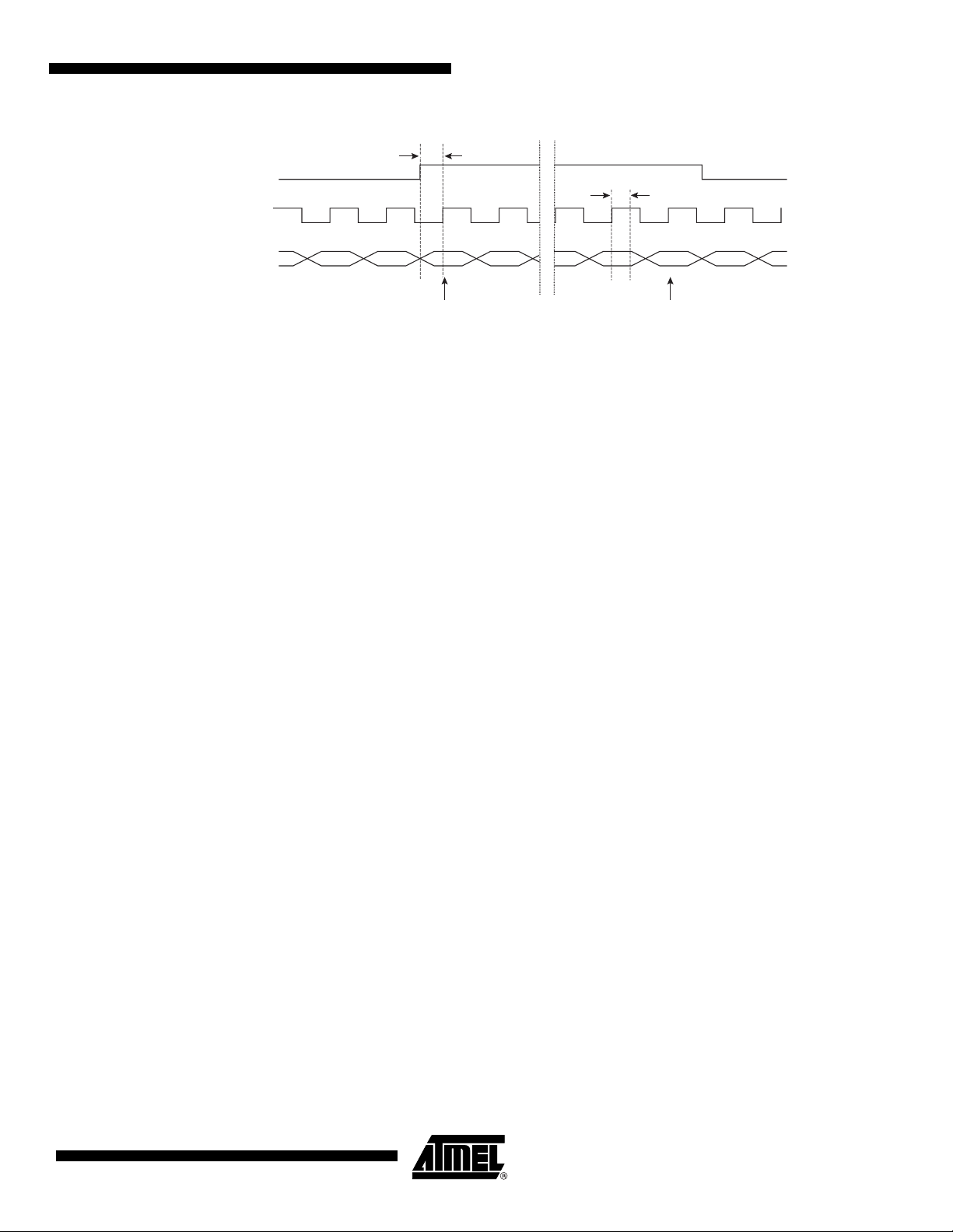
Figure 4-6. Output Data Chronogram
[Preliminary] ATMOS -1M60/1M30
LVAL
STROBE
DATA
ts
th
First Valid Pixel Last Valid Pixel
5429B–IMAGE–04/05
11
Page 12

5. Camera Features
5.1 Region of Interest
The full resolution of the camera is 1312 pixels by 1024 lines.You might program a smaller resolution in order to reduce the readout time. You must be careful that depending on the
sequencing mode, the exposure time can be reduced too.The authorized values for horizontal
size are 32 to 1312 pixels. This value is rounded to the
rized values for vertical size are 32 to 1024 lines. This value is rounded to the lower multiple of 8
lines. See registers ROI area @ 280H, 282H, 284H and 286H Internal Register Mapping on
page 17.
Examples of frame rate versus resolution:
Table 5-1. R.O.I Performance
5.2 Analog Gain
The analog gain can be adjusted by setting the gain register via the serial communication.
lower multiple of 16 pixels. The autho-
ROI Size Frame Rate 1M60 (fps) Frame Rate 1M30 (fps)
1312 × 1024 48 24
1024 × 1024 60 30
640 × 480 175 85
5.3 Subsampling
• Gain adjusted from 0 dB to 18 dB: code 0 to 6
• Step 3 dB
• Nominal gain (factory configuration): 0 dB
See register Sensor Analog Gain @ 240H, Internal Register Mapping on page 17.
– Subsampling 1: All pixels are readout (1312 × 1024)
– Subsampling 2: Two times lower resolution in both axes (656 × 512)
– Subsampling 4: Four times lower resolution in both axes (328 × 256)
See register Subsampling @ 288H, Internal Register Mapping on page 17.
Subsampling parameters might be combined with the ROI. The minimal window size resulting
from these combinations must be at least 32 × 32 pixels. This leads to the following table of minimal ROI size versus Subsampling:
Table 5-2. Subsampling Minimum Size
Subsampling Minimum ROI Size
1 32 × 32
2 64 × 64
4 128 × 128
5.4 Output Format
12
ATMOS -1M60/1M30 [Preliminary]
The data format available on the CameraLink output interface is programmable via the serial
interface.
5429B–IMAGE–04/05
Page 13

5.5 Test Pattern
[Preliminary] ATMOS -1M60/1M30
1. The pixel depth is set by default at 12-bit, it can be set to 10 or 8-bit. The assignment for
each configuration comply with the specifications of the CameraLink interface standard.
See register Mode Control bits [3:2] @ 204H, Internal Register Mapping page 17 .
2. In standard mode the camera provides output data on a single channel of the CameraLink output interface. You might program the camera in two outputs mode, only with
the 1M60. Pixel data is de-multiplexed (odd and even pixels) on ports A, B and C of the
CameraLink interface and STROBE signal is divided by 2 (37.5 MHz).
See register mode control bit [4] @ 204H,Internal Register Mapping page 17 .
In normal mode, the digital video signal from the sensor is available on the CameraLink output
interface. For test purposes a digital pattern is generated and is available instead of the video
signal in the CameraLink output interface. The pattern can be fixed or sliding. The fixed digital
pattern is ramp-up from 960 LSB code to 2271 LSB code (line width). The same pattern is
shown for each line:
Figure 5-1. Test Pattern View
The sliding pattern starts with the fixed pattern, the first code of each line is then incremented by
two on each frame. It is useful to validate the connection to the acquisition system before the
adjustment settings of the image capture. The Subsampling parameter does not affect the
pattern.
See register Mode Control bits [1:0] @ 204H, Internal Register Mapping on page 17.
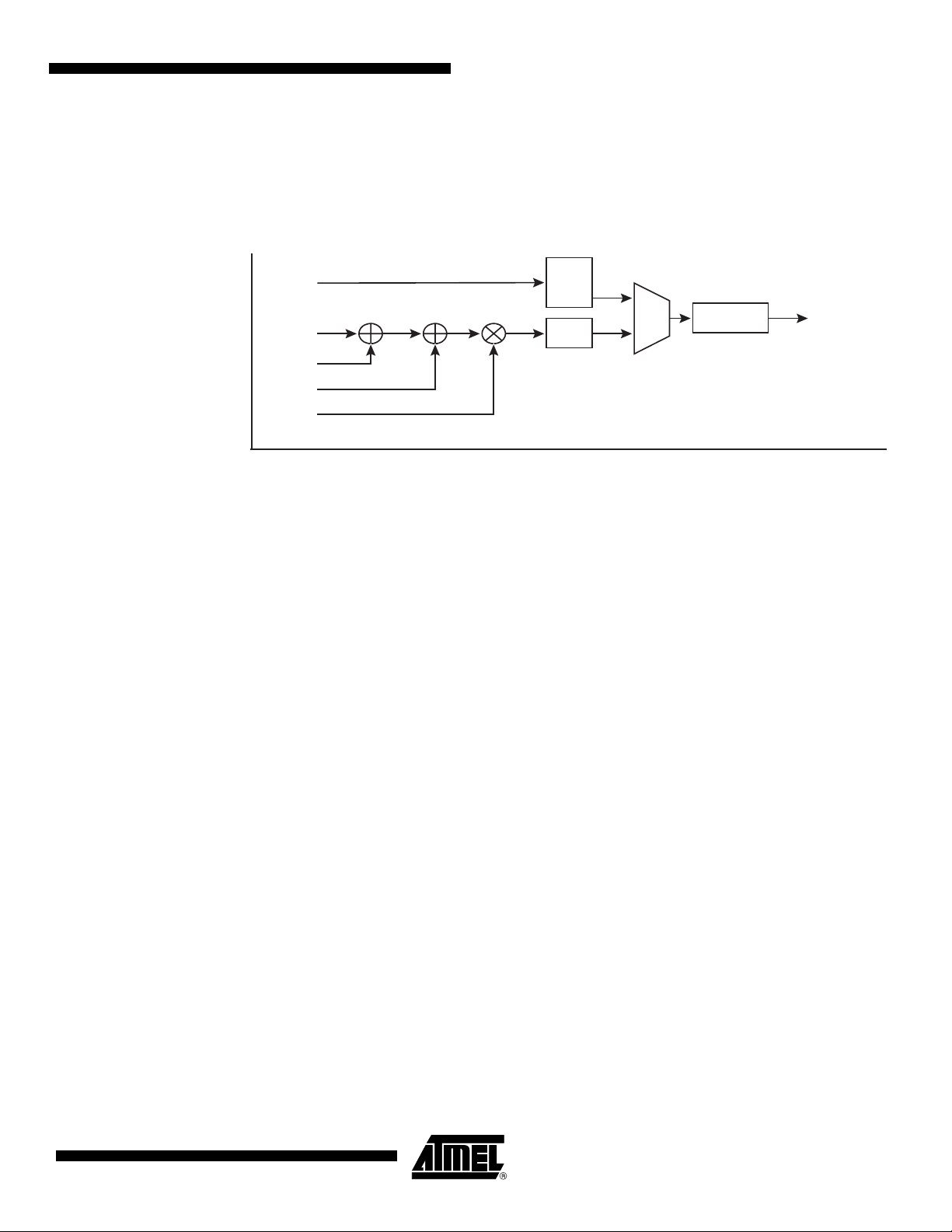
5.6 Contrast Expansion
The digital gain and offset can be adjusted via the serial communication in order to focus on a
particular part of the dynamic range.
• Gain adjusted from x1 to x32.875: code 0 to 255
• Step 0.125
• Nominal gain (factory configuration):
See register Digital Gain @ 242H, Internal Register Mapping on page 17.
• Offset adjusted from -4096 to +4095: code 0 to 8191 in 2's complement
• Step 1
• Nominal offset (factory configuration): 0
See register Digital Offset @ 244H, Internal Register Mapping on page 17.
See register Processing Control bits [1:0] @ 202H, Internal Register Mapping on page 17.
× 1
5429B–IMAGE–04/05
13
Page 14

5.7 Look- up Table (LUT)
The look-up Table is a conversion table which applies to the sensor data. At each input pixel
value corresponds a single output value. This allows you to apply a correction table like a
gamma correction for example.
The Look-up Table might be generated by the camera by programming the gamma setting:
• Gamma 0.125 to 7.875: code 1 to 63 (0 not admitted)
You might also write your own correction table via the serial communication channel. Four banks
are available to store four distinct correction tables.
See register LUT Coefficient Save in Dataflash @ 10DH, Internal Register Mapping on page 17.
See register LUT Coefficient Restore in Dataflash @ 10EH, Internal Register Mapping on page
17.
See register Processing Control bit 2 @ 202H, Internal register mapping on page 17
5.8 Fixed Pattern Noise (FPN) Correction
The fixed pattern noise (FPN) is a spatial fluctuation of the sensor data particularly between successive columns. The purpose is to calculate an offset for each column of the frame in the
darkness. The table of column offsets is stored in the internal memory. If the FPN correction is
then enabled the offset values are subtracted to the value of the input pixel. Two methods are
available to realize this processing: the off-line calibration and the online correction.
5.9 Off-line Calibration
A calibration step is required while the camera is in darkness condition. Offset coefficients for
each column are calculated on an average value measured on all 1024 lines. Offset coefficients
are 8-bit data. Therefore to be efficient the pixel value should be always within the values 1LSB
to 255 LSB. If not, the overflow / underflow flags are set in the status register. The calibration
step must be done in full resolution and subsampling 1. Calibration data can be saved in nonvolatile memory and four distinct banks are reserved for this use. You might access to these banks
in read or write mode.
See register Processing Control bits [4:3] @ 202H, Internal register mapping on page 17.
See register Calibration Control @ 200H, Internal register mapping on page 17.
See register FPN Coefficient Save in Dataflash @ 10BH, Internal register mapping on page 17.
See register FPN Coefficient Restore in Dataflash @ 10CH, Internal Register Mapping on page
17.
5.10 Online Correction
No calibration step is required. When online correction is enabled the camera calculates the offset coefficients for each column on masked lines and then processes the input sensor data.
These coefficients are updated at each frame. The online correction applies only in subsampling
1. The calculated values are less accurate with these methods but unlike the off-line calibration
do not depend on the settings like the analog gain.
14
See register Processing Control bits [4:3] @ 202H, Internal Register Mapping on page 17.
See register FPN Coefficient Save in Dataflash @ 10BH,Internal Register Mapping on page 17.
ATMOS -1M60/1M30 [Preliminary]
5429B–IMAGE–04/05
Page 15
See register FPN Coefficient Restore in Dataflash @ 10CH, Internal Register Mapping on page
t
17.
5.11 Processing Synoptic
Figure 5-2. Synoptic
Pattern
Pixel_In
Coef_FPN
Offset
Gain
[Preliminary] ATMOS -1M60/1M30
C
P
T
Pixel_Ou
LUT
MUX
FORMAT
5.12 LED Indicator
The green LED on the rear panel gives information on the internal state of the camera. On
power up, after internal configuration, the LED flashes on and has the following behavior
(decreasing priority order):
• Internal hardware error or configuration error: fast blinking
• Waiting for external trigger (triggered and ITC modes): slow blinking
• All other situation: continuous
5429B–IMAGE–04/05
15
Page 16

6. Electrical Interface
6.1 Power Supply
It is recommended to insert a 1A fuse between the power supply and the camera. The voltage
ripple of the power supply shall be below ±50 mVp-p at BW = 50 MHz to have full camera
performanceI
Table 6-1. Power Supply Description
Signal Name I/O Type Description
PWR P - DC power input: +12 V to + 24 V
GND P - Electrical and mechanical ground
Note: I = input, O = output, I/O = bi-directional signal, P = power/ground, NC = not connected
6.2 Command and Control
The CameraLink interface provides four LVDS signals dedicated to camera control (CC1 to
CC4). On the ATMOS, one of them is used to synchronize the camera on external events.
Table 6-2. CameraLink Input Description
Signal Name I/O Type Description
TRIG1 I RS644 CC1 - Synchronization input
Note: I = input, O = output, I/O = bi-directional signal, P = power/ground, NC = not connected
The TTL/I/O interface provides two TTL signals dedicated to camera control.
Table 6-3. TTL/IO Description
Signal Name I/O Type Description
TRIGGER I 5 V-TTL External trigger input
SHUTTER O 3 V-TTL
Note: I = input, O = output, I/O = bi-directional signal, P = power/ground, NC = not connected
Shutter output, maximum output current
1.6 mA
See register Mode Control @ 204H, Internal Register Mapping on page 17.Video Data.
Data and enable signals are provided on the CameraLink interface.
Table 6-4. Camera Link Output Description
Signal Name I/O Type Description
ODD-D[11-0] O RS644 Odd pixel data, ODD-00 = LSB, ODD-11 = MSB
EVEN-D[11-0] O RS644 Even pixel data, EVEN-00 = LSB, EVEN-11 = MSB
STROBE O RS644 Output data clock, data valid on the rising edge
LVAL O RS644 Line valid or line enable, active high signal
FVAL O RS644 Frame valid or frame enable, active high signal
16
Note: 1. I = input, O = output, I/O = bi-directional signal, P = power/ground, NC = not connected
2. Note: DVAL, as defined in the CameraLink standard, is not used. DVAL is permanently tied to
1 (high) level.
ATMOS -1M60/1M30 [Preliminary]
5429B–IMAGE–04/05
Page 17

6.3 Serial Communication
The CameraLink interface provides two LVDS signal pairs for the communication between the
camera and the frame grabber. This is an asynchronous serial communication based on RS-232
protocol.
The configuration of the serial line is:
• Full duplex/without handshaking
• 8-bit data, no parity bit, 1 stop bit
• 9600 bauds at power up, then programmable up to 115200 bauds
Table 6-5. CameraLink Serial Communication Description
Signal Name I/O Type Description
[Preliminary] ATMOS -1M60/1M30
SerTFG O RS644
SerTC I RS644
Differential pair for serial communication
to the frame grabber
Differential pair for serial communication
from the frame grabber
6.3.1 Internal Register
Table 6-6. Internal Register Mapping
Access Type
Start Addr
(Hex)
000 1 RO RO
001 1 RW - 1
040 51 RO - Hardware identifier
080 8 RO - Firmware identifier
0C0 51 RW - User identifier
100 4 RW RW Status (ref. Camera Status Management)
104 4 WO -
108 1 RO -
Size
Dec)
End
Addr (Hex)
Processing Internal Task
Factory
Settings Description
Synchronization register for serial
communication (value 00)
Communication speed multiplier (9600 115,2K): volatile register 1, 2, 3, 4, 6, 8, 12
Lock/Unlock mode: advanced user/user
1: Lock advanced user mode
(into user mode)
Unlock key value: unlock user
Privilege level
1: Advanced user mode
2: User mode
109 1 WO -
10A 1 RW - 0
5429B–IMAGE–04/05
Current configuration save in Eeprom
1: User settings (allowed only for advanced
user mode)
2 to 4: User settings
Current configuration restore from Eeprom
1 to 4: User settings
17
Page 18

Table 6-6. Internal Register Mapping (Continued)
Access Type
Start Addr
(Hex)
10B 1 WO -
10C 1 RW - 1
10D 1 WO -
10E 1 RW - 1
200 2 RW RW 0
202 2 RW - 0
Size
Dec)
End
Addr (Hex)
Processing Internal Task
Factory
Settings Description
FPN coefficient save in dataflash
1 to 4 (1 allowed only for advanced user
mode)
FPN coefficient restore in dataflash
1 to 4
LUT coefficient save in dataflash
1 to 4 (1 allowed only for advanced user
mode)
LUT coefficient restore in dataflash
1 to 4
Calibration control
[0] = off-line calibration enabled
(0: disabled; 1: enabled)
Processing control:
[0] = offset correction enable (0: disabled;
1: enabled)
[1] = gain correction enable (0: disabled; 1:
enabled)
[2] = look-up table correction enable (0:
disabled; 1: enabled)[
[4:3] = fpn correction mode (00: disabled;
01: off-line fpn correction enabled; 11: online fpn correction enabled)
204 2 RW - 0
206 1 WO
Mode control:
[1:0] = test pattern (00: disabled; 01: fixed
test pattern; 10: dynamic test pattern)
[3:2] = output format (00:12-bit; 01:10-bit;
10:8-bit)
[4] = demux mode (for 1M60 then 0:
disabled; 1: enabled) (for 1M30 then 0:
disabled)
[7:5] = synchronization mode (000: Freerun; 001: External triggered; 010: external
triggered without full reset; 011: integration
time controlled); others reserved
[8] = trigger source (0: CameraLink; 1:
external)
[9] = trigger polarity (0:positive edge; 1:
negative edge)
[10] = shutter polarity output (0: positive
edge; 1: negative edge)
Software reset:
1 = camera reset
18
ATMOS -1M60/1M30 [Preliminary]
5429B–IMAGE–04/05
Page 19

[Preliminary] ATMOS -1M60/1M30
Table 6-6. Internal Register Mapping (Continued)
Access Type
Start Addr
(Hex)
240 2 RW - 0
242 2 RW - 0
244 2 RW - 0
246 2 RW - 1
248 2 RW - 1600
280 8 287 RW ROI area:
Size
Dec)
End
Addr (Hex)
Processing Internal Task
Factory
Settings Description
Sensor analog gain:
[3:0] = analog gain; value from 0 dB (= 0) to
18 dB (= 6) by step of 3 dB
Digital gain (extended dynamic range):
[7:0] = gain; value from 1.000 (= 0) to
32.875 (= 255) in Q 9.3 representation
Digital offset (extended dynamic range):
[12:0] = offset; value from -4096 to
+ 4095 in 2's complement
Aperture shutter time:
[15:0] = shutter time; value from 0 to 65535
(for 1M60: 0 to 655 ms by step of 10µs)
(for 1M30: 0 to 1310 ms by step of 20µs)
ERS:
[10:0] value from 0% (= 0,Dark) to 100%
(= 1600, clear) in Q11.4 representation
288 1 RW - 1
2C0 2 RW 50
2C2 2 RW 50
2C4 1 RW - 0
Addr 280, size 2, default 0:
ROI horizontal start value (0 to 1311)
Addr 282, size 2, default 0
ROI vertical start value (0 to 1023)
Addr 284, size 2, default 1312
ROI vertical size value from 32 to 1312
Addr 286, size 2, default 1024
ROI vertical size value from 32 to 1024
Subsampling:
[2:0] = Subsampling (001: 1/1; 010: 1/4;
100: 1/16)
Hot pixel detection threshold:
[10:0] = hot pixel threshold
Dead pixel detection threshold:
[10:0] = dead pixel threshold
Defective pixels control:
[0] = hot pixel detection (0: disabled; 1:
enabled
[1] = dead pixel detection (0: disabled; 1:
enabled)
5429B–IMAGE–04/05
19
Page 20

Table 6-6. Internal Register Mapping (Continued)
Access Type
Start Addr
(Hex)
300 1 WO -
1000 1312 151F RW - 0
2000 8192 3FFF RW - linear
Note: RO: Read Only register, WO: Write Only register, RW: Read & Write register
Size
Dec)
End
Addr (Hex)
Processing Internal Task
Factory
Settings Description
6.3.2 Camera Settings Memory
ATMOS cameras have 5 banks to save settings:
• Bank 0 contains the factory settings. This bank cannot be modified by the user
• Bank 1 to 4 are used to store 4 different settings
• Bank 1 might be protected by an advanced user (see Register @ 104H). Contact Atmel for
details
Gamma correction:
[5:0] = gamma settings; value from 0.125
(= 1) to 7.875 (= 63) in Q6.3 representation
FPN coefficients (8-bit):
Format: Fpn [0]; Fpn[1]; Fpn [2];…
Look-up table (4096 × 16-bit):
Format: Lut [0]; Lut [1]; … ; Lut [4095]
value: 0 to 4095
20
ATMOS -1M60/1M30 [Preliminary]
5429B–IMAGE–04/05
Page 21
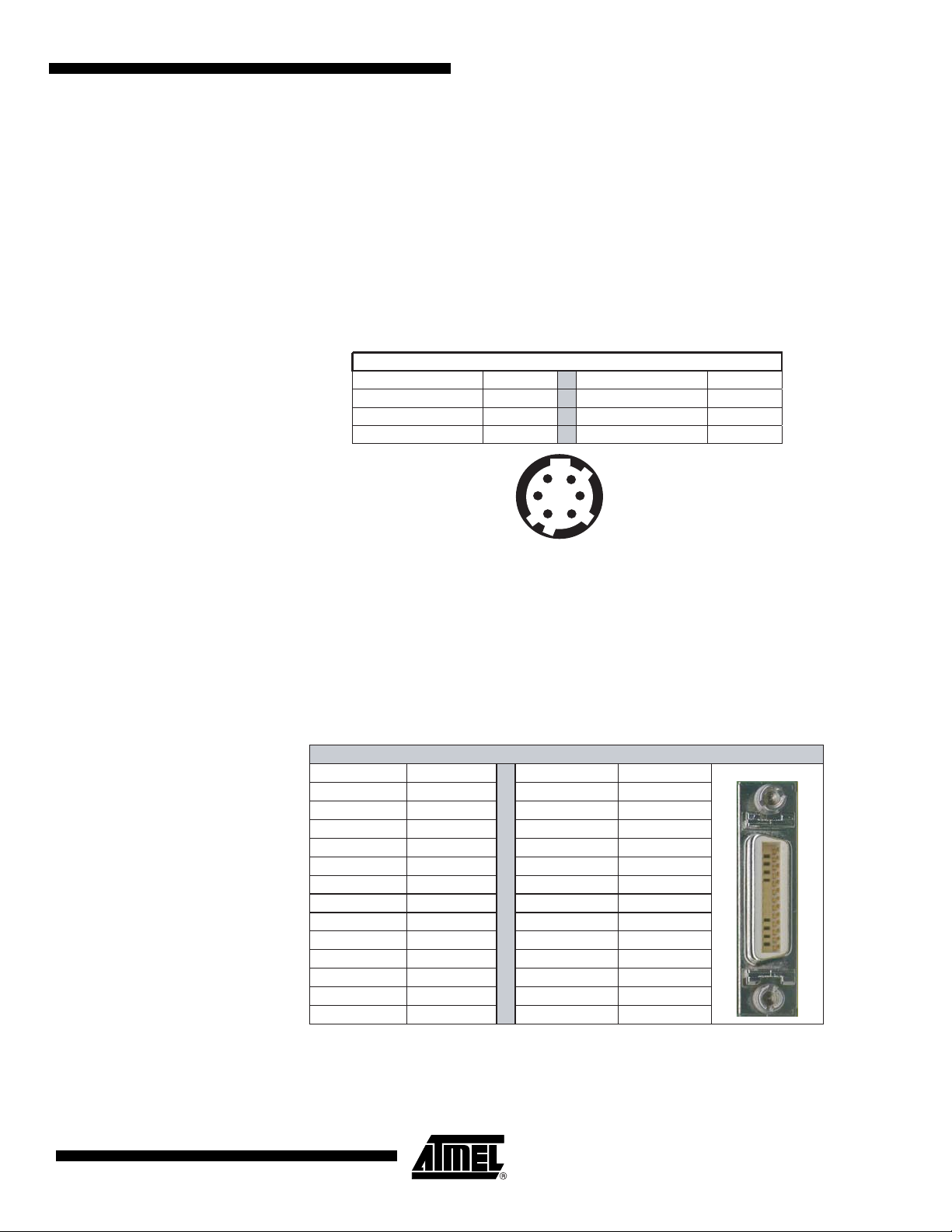
7. Connector Description
All connectors are on the rear panel. Better results are obtained by using shielded cables (foil
and braid shielded).
Note: cables for digital signals shall be twisted pairs.
7.1 Power Supply
Camera connector type: Hirose HR10A-7R-6PB (male)
Cable connector type: Hirose HR10A-7P-6S (female)
Figure 7-1. Power Supply Pinout
[Preliminary] ATMOS -1M60/1M30
Power Connector : J01
Signal Pin Signal Pin
PWR 1 GND 4
NC 2 NC 5
PWR 3 GND 6
7.2 CameraLink Connector
Standard CameraLink cable shall be used to ensure the full electrical compatibility.
• Camera connector type: MDR-26 (female) ref. 3M 10226-2210VE
• We recommend to use a CameraLink standard shielded cable as 3M 14X26-SZLB-XXX-0LC
Figure 7-2. CameraLink Pinout
1
2
3
Receptacle Viewed from Camera Back
Command and Control Connector : J02
Signal Pin Signal Pin
GND 1 GND 14
X0- 2 X0+ 15
X1- 3 X1+ 16
X2- 4 X2+ 17
Xclk- 5 Xclk+ 18
X3- 6 X3+ 19
SerTC+ 7 SerTC- 20
SerTFG- 8 SerTFG+ 21
CC1- 9 CC1+ 22
CC2+ 10 CC2- 23
CC3- 11 CC3+ 24
CC4+ 12 CC4- 25
GND 13 GND 26
6
5
4
5429B–IMAGE–04/05
21
Page 22

7.3 TTL I/O
Camera connector type: Hirose HR10A-7R-5SB (female)
Cable connector type: Hirose HR10A-7P-5P (male)
Figure 7-3. TTL/IO Pinout
TTL IO Connector : J03
Signal Pin Signal Pin
TRIGGER 1 GND 4
GND 2 NC 5
SHUTTER 3
1
4
Receptacle Viewed from Camera Back
2
5
3
22
ATMOS -1M60/1M30 [Preliminary]
5429B–IMAGE–04/05
Page 23

8. Mechanical Drawing
Note: (All dimensions are in mm)
Figure 8-1. Front Panel View
[Preliminary] ATMOS -1M60/1M30
Figure 8-2. Front Panel Mechanical Drawing
44
φ35
sensor
38.5
Note: 1. A and B are mechanical reference plans
2. Sensor alignment ∆x, y refers to the optical axis
3. Sensor alignment ∆0
4 x (M3 x
A
8)
B
First Pixel
of Line 1
1 - 32 UN -
(C mount)
xy
2A
refers to the reference plans
Camera
Link
Power
Supply
2 x (M4 x
(on the 4 sides)
44.75
3.75
12
22
8)
5429B–IMAGE–04/05
23
Page 24

Figure 8-3. Rear Panel
Figure 8-4. Rear Panel Mechanical Drawing
44
12-24V
23
CameraLink
31.30
9.90
TTL IO
22.80
®
24
ATMOS -1M60/1M30 [Preliminary]
5429B–IMAGE–04/05
Page 25

[Preliminary] ATMOS -1M60/1M30
9. Ordering Code
Table 9-1. Ordering Code
Part Number Description
AT71-ATM1M60M-B0
AT71-ATM1M30M-B0
ATMOS 1M60 with housing + power supply connector + TTL I/O
Connector + CD-Rom
ATMOS 1M30 with housing + power supply connector + TTL I/O
Connector + CD-Rom
Delivery:
ATMOS areascan cameras are delivered with:
• Power supply connector HR10A-7P-6S
• TTL I/O connector HR10A-7P-5P
• CD-rom with:
– Friendly software CommCam
– Documentation
5429B–IMAGE–04/05
25
Page 26

Atmel Corporation Atmel Operations
2325 Orchard Parkway
San Jose, CA 95131, USA
Tel: 1(408) 441-0311
Fax: 1(408) 487-2600
Regional Headquarters
Europe
Atmel Sarl
Route des Arsenaux 41
Case Postale 80
CH-1705 Fribourg
Switzerland
Tel: (41) 26-426-5555
Fax: (41) 26-426-5500
Asia
Room 1219
Chinachem Golden Plaza
77 Mody Road Tsimshatsui
East Kowloon
Hong Kong
Tel: (852) 2721-9778
Fax: (852) 2722-1369
Japan
9F, Tonetsu Shinkawa Bldg.
1-24-8 Shinkawa
Chuo-ku, Tokyo 104-0033
Japan
Tel: (81) 3-3523-3551
Fax: (81) 3-3523-7581
Memory
2325 Orchard Parkway
San Jose, CA 95131, USA
Tel: 1(408) 441-0311
Fax: 1(408) 436-4314
Microcontrollers
2325 Orchard Parkway
San Jose, CA 95131, USA
Tel: 1(408) 441-0311
Fax: 1(408) 436-4314
La Chantrerie
BP 70602
44306 Nantes Cedex 3, France
Tel: (33) 2-40-18-18-18
Fax: (33) 2-40-18-19-60
ASIC/ASSP/Smart Cards
Zone Industrielle
13106 Rousset Cedex, France
Tel: (33) 4-42-53-60-00
Fax: (33) 4-42-53-60-01
1150 East Cheyenne Mtn. Blvd.
Colorado Springs, CO 80906, USA
Tel: 1(719) 576-3300
Fax: 1(719) 540-1759
Scottish Enterprise Technology Park
Maxwell Building
East Kilbride G75 0QR, Scotland
Tel: (44) 1355-803-000
Fax: (44) 1355-242-743
RF/Automotive
Theresienstrasse 2
Postfach 3535
74025 Heilbronn, Germany
Tel: (49) 71-31-67-0
Fax: (49) 71-31-67-2340
1150 East Cheyenne Mtn. Blvd.
Colorado Springs, CO 80906, USA
Tel: 1(719) 576-3300
Fax: 1(719) 540-1759
Biometrics/Imaging/Hi-Rel MPU/
High Speed Converters/RF Datacom
Avenue de Rochepleine
BP 123
38521 Saint-Egreve Cedex, France
Tel: (33) 4-76-58-30-00
Fax: (33) 4-76-58-34-80
Literature Requests
www.atmel.com/literature
Disclaimer: The information in this document is provided in connection with Atmel products. No license, express or implied, by estoppel or otherwise, to any
intellectual property right is granted by this document or in connection with the sale of Atmel products. EXCEPT AS SET FORTH IN ATMEL’S TERMS AND CONDI-
TIONS OF SALE LOCATED ON ATMEL’S WEB SITE, ATMEL ASSUMES NO LIABILITY WHATSOEVER AND DISCLAIMS ANY EXPRESS, IMPLIED OR STATUTORY
WARRANTY RELATING TO ITS PRODUCTS INCLUDING, BUT NOT LIMITED TO, THE IMPLIED WARRANTY OF MERCHANTABILITY, FITNESS FOR A PARTICULAR
PURPOSE, OR NON-INFRINGEMENT. IN NO EVENT SHALL ATMEL BE LIABLE FOR ANY DIRECT, INDIRECT, CONSEQUENTIAL, PUNITIVE, SPECIAL OR INCIDENTAL DAMAGES (INCLUDING, WITHOUT LIMITATION, DAMAGES FOR LOSS OF PROFITS, BUSINESS INTERRUPTION, OR LOSS OF INFORMATION) ARISING OUT
OF THE USE OR INABILITY TO USE THIS DOCUMENT, EVEN IF ATMEL HAS BEEN ADVISED OF THE POSSIBILITY OF SUCH DAMAGES. Atmel makes no
representations or warranties with respect to the accuracy or completeness of the contents of this document and reserves the right to make changes to specifications
and product descriptions at any time without notice. Atmel does not make any commitment to update the information contained herein. Atmel’s products are not
intended, authorized, or warranted for use as components in applications intended to support or sustain life.
© Atmel Corporation 2005. All rights reserved. Atmel®, logo and combinations thereof, and Dataflash® are registered trademarks, and Every-
where You Are
Imaging Association. Other terms and product names may be trademarks of others.
SM
, ATMOS™and others are trademarks of Atmel Corporation or its subsidiaries. CameraLink® is the trademark of Automated
Printed on recycled paper.
5429B–IMAGE–04/05
xM
 Loading...