

Page 1

Features
• High Performance, Low Power AVR
• Advanced RISC Architecture
– 124 Powerful Instructions - Most Single Clock Cycle Execution
– 32 x 8 General Purpose Working Registers
– Fully Static Operation
– Up to 4 MIPS Throughput at 4 MHz
• Nonvolatile Program and Data Memories
– 4K/8K Bytes of In-System Self-Programmable Flash (ATmega4HVD/8HVD)
– 256 Bytes EEPROM
– 512 Bytes Internal SRAM
– Write/Erase Cycles: 10,000 Flash/ 100,000 EEPROM
– Data Retention: 20 years at 85°C /100 years at 25°C
– Programming Lock for Software Security
• Battery Management Features
– One Cell Batteries
– Short-circuit Protection (Discharge)
– Over-current Protection (Charge and Discharge)
– External Protection Input
– High Voltage Outputs to Drive N-Channel Charge/Discharge FETs
– Operation with 1 FET or 2 FETs supported
Charge FET is optional
– Battery authentication features (Availab le only under NDA)
• Peripheral Features
– Two 8/16-bit Timer/Counters with Separate Prescaler and two output compare
units
– 10-bit ADC with One External Input
– Two High-voltage open-drain I/O pins
– Programmable Watchdog Timer
• Special Microcontroller Features
– debugWIRE On-chip Debug System
– In-System Programmable
– Power-on Reset
– On-chip Voltage Reference with built-in Temperature Sensor
– On-chip Voltage Regulator
– External and Internal Interrupt Sources
– Sleep Modes:
Idle, ADC Noise Reduction, Power-save, and Power-off
• Package
– 18-pad DRDFN/ MLF
• Operating Voltage (VFET): 2.1 - 6.0V
• Operating Voltage (V
• Maximum Withstand Voltage (VFET): 12V
• Maximum Withstand Voltage (High-voltage pins): 5V
• Temperature Range: -20°C to 85°C
• Speed Grade: 1 - 4 MHz
):2.0 - 2.4V
CC
®
8-bit Microcontroller
(1)
8-bit
Microcontroller
with 4K/8K
Bytes In-System
Programmable
Flash
ATmega4HVD
ATmega8HVD
Preliminary
8052B–AVR–09/08
Page 2
1. Pin Configurations
Figure 1-1. Dual Row DFN/ MLF-pinout ATmega4HVD/8HVD.
Top view
Bottom view
B10
A8
B9
A7
B8
A6
B7
A5
B6
Table 1-1. Dual Row DFN/ MLF-pinout ATmega4HVD/8HVD.
123 4 5 6 7 8 9 10
PB1
DNC BATT GND PV1
A
OD OC VFET VREG NI
B
(SCK/
SGND/T0)
DNC VCC
PB0
(ADC0)
(MISO/CKOUT/T1)
PB2
B1
B2
B3
B4
B5
PC1
(MOSI/INT1/
EXT_PROT)
GND
A1
A2
A3
A4
--
PC0
(INT0/ICP0/XTAL)
RESET
2
ATmega4HVD/8HVD
8052B–AVR–09/08
Page 3

1.1 Pin Descriptions
1.1.1 VFET
1.1.2 VCC
1.1.3 VREG
1.1.4 GND
1.1.5 Port B (PB2:PB0)
ATmega4HVD/8HVD
Input to the internal voltage regulator.
Pin for connection of external decoupling capaci tor. VCC is internally connected t o the voltage
regulator output VREG.
Output from the internal voltage regulator . Int er n ally co nnected to VCC.
Ground
Port B is a low-voltage 3-bit bi-directional I/O port with internal pull-up resistors (selected for
each bit). As inputs, Port B pins that are externally pulled low will source current if the pull-up
resistors are activated. The Port B pins are tri-stated when a reset condition becomes active,
even if the clock is not running.
1.1.6 Port C (PC1:PC0)
1.1.7 OC
1.1.8 OD
1.1.9 NI
1.1.10 PV1
1.1.11 BATT
1.1.12 RESET
/dw
Port B also serves the functions of various special features of the ATmega4HVD/8HVD.
Port C is a High-voltage open-drain 2 bit bi-directional I/O port. Port C also serves the functions of various special features of the ATmega4HVD/8HVD.
High voltage output to drive Charge FET (optional).
High voltage output to drive Discharge FET.
Negative input from the battery protection resistor.
Input from battery cell to ADC.
Input for detecting when a charger is connected.
8052B–AVR–09/08
Reset input. A low level on this pin for longer than the minimum pulse length will generate a
reset, even if the clock is not running. Shorter pulses are not guaranteed to generate a reset.
This pin is also used as debugWIRE communication pin.
3
Page 4
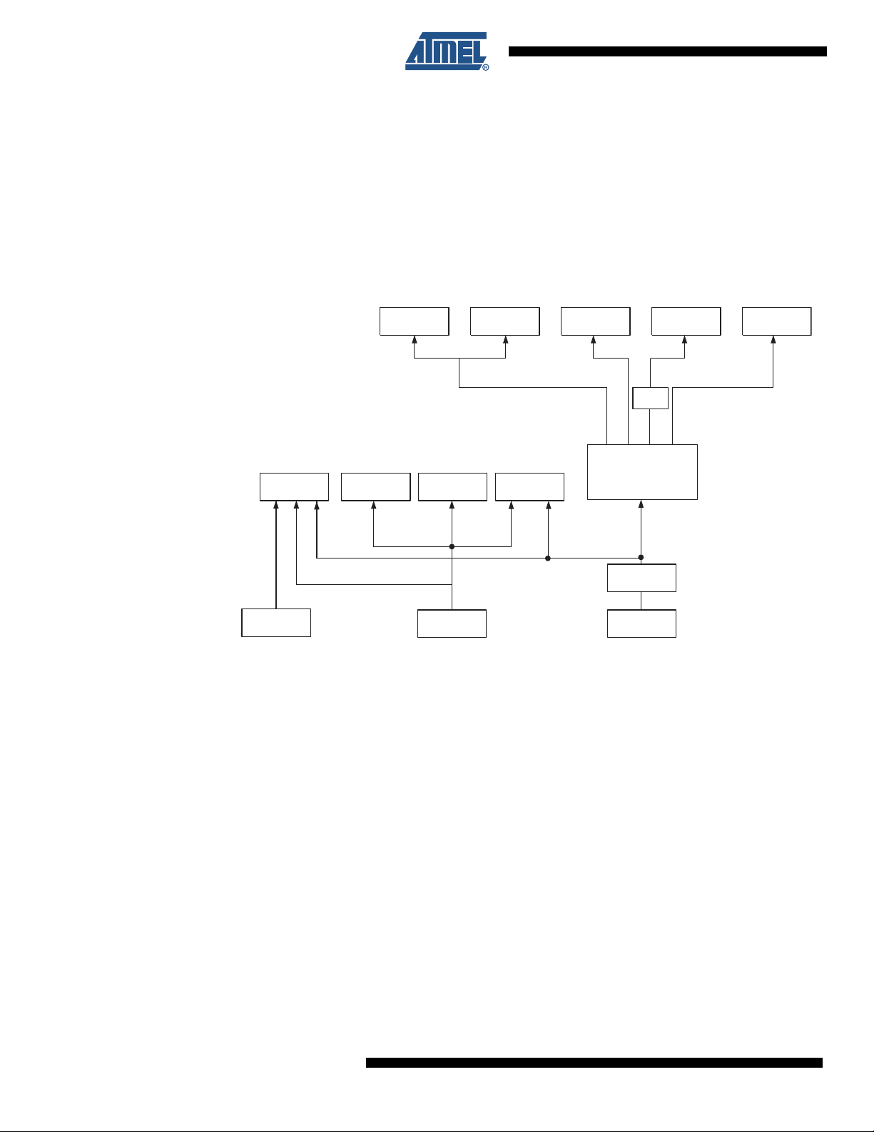
2. Overview
PORTC (2)
SRAMFlash
CPU
EEPROM
GND
OC
OD
FET
Control
Voltage
ADC
Voltage
Reference
GND
VCC
RESET/dW
Power
Supervision
POR &
RESET
Watchdog
Oscillator
Watchdog
Timer
Oscillator
Circuits /
Clock
Generation
PC1:0
8/16-bit T/C1
8/16-bit T/C0
PORTB (3)
PB2:0
SPI
Voltage
Regulator
Charger
Detect
VFET
VREG
BATT
PV1
DATA BUS
Battery
Protection
Security
Module
Voltage Regulator
Monitor Interface
PB2 (CKOUT)
Oscillator
Sampling
Interface
Program
Logic
debugWIRE
NI
PC1 (External Protection Input)
PB0 (ADC0)
The ATmega4HVD/8HVD is a monitoring and protection circuit for 1-cell Li-ion applications
with focus on high security/authentication, low cost and high utilization of the cell energy. The
device contains secure authentication features as well as autonomous battery protection during charging and discharging. The External Protection Input can be used to implement other
battery protection mechanisms using external components, e.g. protection against chargers
with too high charge voltage can be easily implemented with a few low cost passive components. The feature set makes the ATmega4HVD/8HVD a key component in any system
focusing on high security, battery protection, high system utilization and low cost.
Figure 2-1. Block Diagram
An integrated, low-dropout linear regulator that can handle input voltages as low as 2.1V,
ensures that the stored energy can be fully exploited. The regulator capabilities, combined
with a extremely low power consumption in the powe r saving modes, greatly enhances th e cell
energy utilization compared to existing solutions.
The chip utilizes Atmel's Deep Under-voltage Recovery (DUVR) mode that supports precharging of deeply discharged battery cells without using a separate Pre-charge FET. An
enhanced start-up scheme allows the chip to operate correctly even with only Discharge FET
connected. This makes it possible to further reduce system cost for applications that do not
require Charge Over-current protection.
The ATmega4HVD/8HVD contains a 10-bit ADC for cell voltage measurem ents. The ADC is
also used to monitor the on-chip temperature. Temp erature is measured by the integrate d
4
ATmega4HVD/8HVD
Voltage Reference, which contains a built-in temperature sensor. ATmega4HVD/8HVD con-
8052B–AVR–09/08
Page 5

ATmega4HVD/8HVD
tains a high-voltage tolerant, open-drain IO pin that supports serial communication.
Programming can be done in-system using the 4 General Purpose IO ports that support SPI
programming
The MCU includes 4K/8K bytes of In-System Programmable Flash with Self-programming
capabilities, 256 bytes EEPROM, 512 bytes SRAM, 32 general purpose working registers, 4
general purpose I/O lines, debug WIRE f or On- chip debug ging and SPI f or In- system Progr amming, two flexible Timer/Counters with Input Capture, internal and external interrupts, a 10-bit
ADC for measuring the cell voltage and on-chip temperature, a prog rammable Watchdog
Timer with wake-up capabilities, and software selectable power saving modes.
The AVR core combines a rich instruction set with 32 general purpose working registers. All
the 32 registers are directly connected to the Arithmetic Logic Unit (ALU), allowing two independent registers to be accessed in one single instruction executed in one clock cycle. The
resulting architecture is more code efficient while achieving throughputs up to ten times faster
than conventional CISC microcontrollers.
The device is manufactured using Atmel’s high voltage high density non-volatile memory technology. The On-chip ISP Flash allows the prog ram memory to be re programmed In-Syst em,
by a conventional non-volatile memory programmer or by an On-chip Boot program running
on the AVR core.
The ATmega4HVD/8HVD AVR is supported with a full suite of program and system development tools including: C Compilers, Macro Assemblers, Program Debugger/Simulators, and
On-chip Debugger.
The ATmega4HVD/8HVD is a low-power CMOS 8-bit microcontroller based on the AVR architecture. It is part of the AVR Smart Battery family that provid es secure authenticat ion, highly
accurate monitoring and autonomous protection for Lithium-ion battery cells.
3. Resources
A comprehensive set of development tools, application notes and datasheets are available for
download on http://www.atmel.com/avr.
Note: 1.
4. Data Retention
Reliability Qualification results show that the projected data retention failure rate is much less
than 1 PPM over 20 years at 85°C or 100 years at 25°C.
5. About Code Examples
This documentation contains simple code examples th at brief ly sho w h ow to use var ious pa rt s
of the device. These code examples assume that the part specific header file is included
before compilation. Be aware that not a ll C compiler vendors inclu de bit definitions in the
header files and interrupt handling in C is compiler depende nt. Ple ase confirm with the C compiler documentation for more details.
8052B–AVR–09/08
For I/O Registers located in extended I/O map, "IN", "OUT", "SBIS", "SBIC", "CBI", and "SBI"
instru0ctions must be replaced with instructions that allow access to extended I/O. Typically
"LDS" and "STS" combined with "SBRS", "SBRC", "SBR", and "CBR".
5
Page 6
6. AVR CPU Core
Flash
Program
Memory
Instruction
Register
Instruction
Decoder
Program
Counter
Control Lines
32 x
8
General
Purpose
Registrers
ALU
Status
and Control
I/O Lines
EEPROM
Data Bus 8-bit
Data
SRAM
Direct Addressing
Indirect Addressing
Interrupt
Unit
Watchdog
Timer
I/O Module 2
I/O Module1
I/O Module n
6.1 Overview
This section discusses the AVR core architecture in general. The main function of the CPU core
is to ensure correct program execution. The CPU must therefore be able to access memories,
perform calculations, control peripherals, and handle interrupts.
Figure 6-1. Block Diagram of the AVR Architecture
In order to maximize performance and parallelism, the AVR uses a Harvard architecture – with
separate memories and buses for program and data. Instructions in the program memory are
executed with a single level pipelining. While one instruction is being executed, the next instruction is pre-fetched from the program memory. This concept enables instructions to be executed
in every clock cycle. The program memory is In-System Reprogrammable Flash memory.
The fast-access Register File contains 32 x 8-bit general purpose working registers with a single
clock cycle access time. This allows single-cycle Arithmetic Logic Unit (ALU) operation. In a typical ALU operation, two operands are output from the Register File, the operation is executed,
and the result is stored back in the Register File – in one clock cycle.
6
ATmega4HVD/8HVD
8052B–AVR–09/08
Page 7

ATmega4HVD/8HVD
Six of the 32 registers can be used as three 16-bit indirect address register pointers for Data
Space addressing – enabling efficient address calcula tions. One of the these addr ess pointer s
can also be used as an address pointer for look up tables in Flash program memory. These
added function registers are the 16-bit X-, Y-, and Z-register, described later in this section.
The ALU supports arithmetic and logic operations between registers or between a constant
and a register. Single register operations can also be executed in the ALU. After an arithmetic
operation, the Status Register is up dated to reflect information abou t the result of the
operation.
Program flow is provided by conditional and unconditional jump and call instructions, able to
directly address the whole address space. Most AVR instructions have a single 16-bit word
format. Every program memory address contains a 16- or 32-bit instruction.
During interrupts and subroutine calls, the return address Program Counter (PC) is stored on
the Stack. The Stack is effectively allocated in the general data SRAM, and consequently the
Stack size is only limited by the total SRAM size and the usage of the SRAM. All user programs must initialize the SP in the Reset routine (be fore subroutines or interrupts are
executed). The Stack Pointer (SP) is read/write accessible in the I/O space. The data SRAM
can easily be accessed through the five different addressing modes supporte d in the AVR
architecture.
The memory spaces in the AVR architecture are all linear and regular memory maps.
A flexible interrupt module has its control registers in the I/O space with an additional Global
Interrupt Enable bit in the Status Register. All interrupt s have a separa te Interrup t Vector in t he
Interrupt Vector table. The interrupts have priority in accordance with their Interrupt Vector
position. The lower the Interrupt Vector addr es s, th e hig he r th e pr ior i ty.
The I/O memory space contains 64 addresses for CPU peripheral functions as Control Registers, SPI, and other I/O functions. The I/O Memory can be accessed directly, or as the Data
Space locations following those of the Register File, 0x20 - 0x5F. In addition, the
ATmega4HVD/8HVD has Extended I/O space from 0x60 - 0xFF in SRAM where only the
ST/STS/STD and LD/LDS/LDD instructions can be used.
6.2 ALU – Arithmetic Logic Unit
The high-performance AVR ALU operates in direct connection with all the 32 general purpose
working registers. Within a single clock cycle, arithmetic operations between general purpose
registers or between a register and an immediate are executed. The ALU operations are
divided into three main categories – arithmetic, logical, and bit-functions. Some implementations of the architecture also provide a powerful multiplier supporting both signed/unsigned
multiplication and fractional format. See the “Instruction Set” section for a detailed description.
6.3 Status Register
The Status Register contains information about the result of the most recently executed arithmetic instruction. This information can be used for altering program flow in order to perform
conditional operations. Note that the Status Register is updated after all ALU operations, as
specified in the Instruction Set Reference. This will in many cases remove the need for using
the dedicated compare instructions, resulting in faster and more compact code.
8052B–AVR–09/08
The Status Register is not automatically stored when entering an interrupt routine and
restored when returning from an interrupt. This must be handled by software.
7
Page 8

6.3.1 SREG – AVR Status Register
Bit 76543210
Read/Write R/W R/W R/W R/W R/W R/W R/W R/W
Initial Value 0 0 0 0 0 0 0 0
• Bit 7 – I: Global Interrupt Enable
The Global Interrupt Enable bit must be set for the interrupts to be enabled. The individual
interrupt enable control is then performed in separate control registers. If the Global Interrupt
Enable Register is cleared, none of the interrupts are enabled independent of the individual
interrupt enable settings. The I-bit is cleared by hardware after an interrupt has occurred, and
is set by the RETI instruction to enable subsequent interrupts. The I-bit can also be set and
cleared by the application with the SEI and CLI instru ctions, as describ ed in the instruction set
reference.
• Bit 6 – T: Bit Copy Storage
The Bit Copy instructions BLD (Bit LoaD) and BST (Bit STore) use the T-bit as source or destination for the operated bit. A bit from a register in the Registe r File can be copied into T by
the BST instruction, and a bit in T can be copied into a bit in a register in the Register File by
the BLD instruction.
ITHSVNZCSREG
• Bit 5 – H: Half Carry Flag
The Half Carry Flag H indicates a Half Carry in some arithmetic operations. Half Carry Is useful in BCD arithmetic. See the “Instruction Set Description” for detailed information.
• Bit 4 – S: Sign Bit, S = N
⊕ V
The S-bit is always an exclusive or between the negative flag N and the Two’s Complement
Overflow Flag V. See the “Instruction Set Description” for detailed information.
• Bit 3 – V: Two’s Complement Overflow Flag
The Two’s Complement Overflow Flag V supports two’s complement arithmetics. See the
“Instruction Set Description” for detailed information.
• Bit 2 – N: Negative Flag
The Negative Flag N indicates a negative result in an arithm etic or logic operation. See th e
“Instruction Set Description” for detailed information.
• Bit 1 – Z: Zero Flag
The Zero Flag Z indicates a zero result in an arithmetic or logic operation. See the “Instruction
Set Description” for detailed information.
• Bit 0 – C: Carry Flag
The Carry Flag C indicates a carry in an arithmetic or logic operation. See the “Instruction Set
Description” for detailed information.
8
ATmega4HVD/8HVD
8052B–AVR–09/08
Page 9

6.4 General Purpose Register File
The Register File is optimized for the AVR Enhanced RISC instruction set. In order to achieve
the required performance and flexibility, the following input/output schemes are supported by
the Register File:
• One 8-bit output operand and one 8-bit result input
• Two 8-bit output operands and one 8-bit result input
• Two 8-bit output operands and one 16-bit result input
• One 16-bit output operand and one 16-bit result input
Figure 6-2 shows the structure of the 32 general purpose working registers in the CPU.
Figure 6-2. AVR CPU General Purpose Working Registers
General R14 0x0E
Purpose R15 0x0F
Working R16 0x10
Registers R17 0x11
ATmega4HVD/8HVD
7 0 Addr.
R0 0x00
R1 0x01
R2 0x02
…
R13 0x0D
…
R26 0x1A X-register Low Byte
R27 0x1B X-register High Byte
R28 0x1C Y-register Low Byte
R29 0x1D Y-register High Byte
R30 0x1E Z-register Low Byte
R31 0x1F Z-register High Byte
Most of the instructions operating on the Register File have direct access to all registers, and
most of them are single cycle instructions.
As shown in Figure 6-2, each register is also assigned a data m emory addre ss, ma pping them
directly into the first 32 locat ions of th e us er Da ta Sp ace. Altho ugh no t be ing physic ally im plemented as SRAM locations, this memory organization provides great flexibility in access of the
registers, as the X-, Y- and Z-pointer registers can be set to index any register in the file.
6.4.1 The X-register, Y-regis ter, and Z-register
The registers R26..R31 have some added functions to their general purpose usage. These
registers are 16-bit address pointers for indirect addressing of the data space. The three indirect address registers X, Y, and Z are defined as described in Figure 6-3.
8052B–AVR–09/08
9
Page 10
6.5 Stack Pointer
Figure 6-3. The X-, Y-, and Z-registers
15 XH XL 0
X-register 707 0
R27 (0x1B) R26 (0x1A)
15 YH YL 0
Y-register 707 0
R29 (0x1D) R28 (0x1C)
15 ZH ZL 0
Z-register 70 7 0
R31 (0x1F) R30 (0x1E)
In the different addressing modes these address registers have functions as fixed disp lacement, automatic increment, and automatic decrement (see the instruction set reference for
details).
The Stack is mainly used for storing temporary data, for storing local variables and for storing
return addresses after interrupts and subroutine calls. The Stack Pointer Register always
points to the top of the Stack. Note that the Stack is implemented as growing from higher
memory locations to lower memory locations. This implies that a Stack PUSH command
decreases the Stack Pointer.
The Stack Pointer points to the data SRAM Stack area where the Subroutine and Interrupt
Stacks are located. This Stack space in the data SRAM must be defined by the program
before any subroutine calls are executed or interrup ts ar e en abled. Th e Sta ck Pointe r mu st be
set to point above 0x100. The Stack Pointer is decremented by one when data is pushed onto
the Stack with the PUSH instruction, and it is decremented by two when the return address is
pushed onto the Stack with subroutine call or interrupt. The Stack Pointer is incremented by
one when data is popped from the Stack with th e POP instruct ion, and it is incre mented by two
when data is popped from the Stack with return from subroutine RET or return from interrupt
RETI.
The AVR Stack Pointer is implemented as two 8-bit registers in the I/O space. The number of
bits actually used is implementation dependent. Note that the data spa ce in some implement ations of the AVR architecture is so small that only SPL is needed. In this case, the SPH
Register will not be present.
6.5.1 SPH and SPL – Stack pointer High and Low Register
Bit 151413121110 9 8
SP15 SP14 SP13 SP12 SP11 SP10 SP9 SP8 SPH
SP7 SP6 SP5 SP4 SP3 SP2 SP1 SP0 SPL
76543210
Read/Write R/W R/W R/W R/W R/W R/W R/W R/W
R/W R/W R/W R/W R/W R/W R/W R/W
Initial Value00000010
11111111
10
ATmega4HVD/8HVD
8052B–AVR–09/08
Page 11
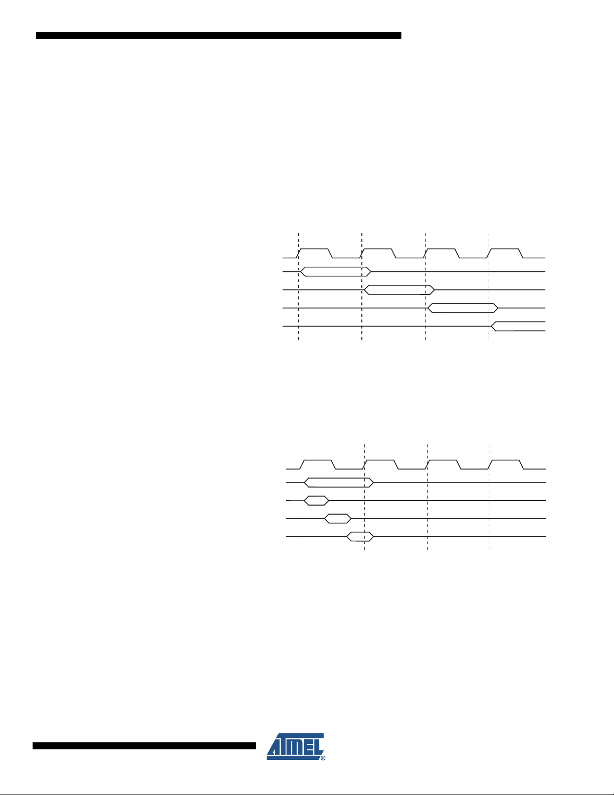
6.6 Instruction Execution Timing
Total Execution Time
Register Operands Fetch
ALU Operation Execute
Result Write Back
T1 T2 T3 T4
clk
CPU
This section describes the general access timing concepts for instruction execution. The AVR
CPU is driven by the CPU clock clk
the chip. No internal clock division is used.
Figure 6-4 shows the parallel instruction fetches and instruction executions enabled by the
Harvard architecture and the fast-access Register File concept. This is the basic pipelining
concept to obtain up to 1 MIPS per MHz with the corresponding unique results for functions
per cost, functions per clocks, and functions per power-unit.
Figure 6-4. The Parallel Instruction Fetches and Instruction Executions
1st Instruction Fetch
1st Instruction Execute
2nd Instruction Fetch
2nd Instruction Execute
3rd Instruction Fetch
3rd Instruction Execute
4th Instruction Fetch
clk
CPU
ATmega4HVD/8HVD
, directly generated from the selected clock source for
CPU
T1 T2 T3 T4
Figure 6-5 shows the internal timing concept for the Register File. In a single clock cycle an
ALU operation using two register operands is executed, and the result is stored back to the
destination register.
Figure 6-5. Single Cycle ALU Operation
6.7 Reset and Interrupt Handling
The AVR provides several different interrupt sources. These inte rrupts and the sepa rate Reset
Vector each have a separate program vector in the program memory space. All interrupts are
assigned individual enable bits which must be written logic one together with the Global Interrupt Enable bit in the Status Register in order to enable the interrupt.
The lowest addresses in the program memory space are by default defined as the Reset and
Interrupt Vectors. The complete list of vectors is shown in ”Interrupts” on page 51. The list also
determines the priority levels of the different interrupt s. The lower the addr ess the higher is the
priority level. RESET has the highest priority.
8052B–AVR–09/08
11
Page 12

When an interrupt occurs, the Global Interrupt Enable I-bit is cleared and all interrupts are disabled. The user software can write logic one to the I-bit to enable nested interrupts. All
enabled interrupts can then interrupt the current interrupt routine. The I-bit is automatically set
when a Return from Interrupt instruction – RETI – is executed.
There are basically two types of interrupts. The first type is triggered by an event that sets the
interrupt flag. For these interrupts, the Program Counter is vectored to the actual Interrupt
Vector in order to execute the interrupt handling routine, and hardware clears the corresponding interrupt flag. Interrupt flags can also be cleared by writing a logic one to the flag bit
position(s) to be cleared. If an interrupt condition occurs while the corresponding interrupt
enable bit is cleared, the interrupt flag will be set and remembered until the interrupt is
enabled, or the flag is cleared by software. Similarly, if one or more interrupt conditions occur
while the Global Interrupt Enable bit is cleared, the corresponding interrupt flag(s) will be set
and remembered until the Global Interrupt Enable bit is set, and will then be executed by order
of priority.
The second type of interrupts will trigger as long as the interrupt condition is present. These
interrupts do not necessarily have interrupt flags. If the interrupt condition disappears before
the interrupt is enabled, the interrupt will not be triggered.
When the AVR exits from an interrupt, it will always return to the main program and execute
one more instruction before any pending interrup t is served.
Note that the Status Register is not automatically stored when entering an interrupt routine,
nor restored when returning from an interrup t routine. This must be handled by software.
When using the CLI instruction to disable interrupts, the interrupts will be immediately disabled. No interrupt will be executed after the CLI instruction, even if it occurs simultaneously
with the CLI instruction. The following example shows how this can be use d to avoid interrupts
during the timed EEPROM write sequence.
Assembly Code Example
in r16, SREG ; store SREG value
cli ; disable interrupts during timed sequence
sbi EECR, EEMWE ; start EEPROM write
sbi EECR, EEWE
out SREG, r16 ; restore SREG value (I-bit)
C Code Example
char cSREG;
cSREG = SREG; /* store SREG value */
/* disable interrupts during timed sequence */
_CLI();
EECR |= (1<<EEMWE); /* start EEPROM write */
EECR |= (1<<EEWE);
SREG = cSREG; /* restore SREG value (I-bit) */
12
ATmega4HVD/8HVD
8052B–AVR–09/08
Page 13

When using the SEI instruction to enable interrupts, the instruction following SEI will be executed before any pending interrupts, as shown in this example.
Assembly Code Example
sei ; set Global Interrupt Enable
sleep; enter sleep, waiting for interrupt
; note: will enter sleep before any pending
; interrupt(s)
C Code Example
_SEI(); /* set Global Interrupt Enable */
_SLEEP(); /* enter sleep, waiting for interrupt */
/* note: will enter sleep before any pending interrupt(s) */
6.7.1 Interrupt Response Time
The interrupt execution response for all the enabled AVR interrupts is four clock cycles minimum. After four clock cycles the progr am vector address for th e actual interrupt hand ling
routine is executed. During this four clock cycle period, the Program Counter is pushed onto
the Stack. The vector is normally a jump to the interrupt routine, and this jump takes three
clock cycles. If an interrupt occurs during execution of a multi-cycle instruction, this instruction
is completed before the interrupt is served. If an interrupt occurs when the MCU is in sleep
mode, the interrupt execution response time is increased by four clock cycles. This increase
comes in addition to the start-up time from the selected sleep mode.
ATmega4HVD/8HVD
A return from an interrupt handling routine takes four clock cycles. During these four clock
cycles, the Program Counter (two bytes) is popped back from the Stack, the Stack Pointer is
incremented by two, and the I-bit in SREG is set.
8052B–AVR–09/08
13
Page 14

7. AVR Memories
7.1 Overview
This section describes the different memories in the ATmega4HVD/8HVD. The AVR architecture has two main memory spaces, the Data Memory and the Program Memory space. In
addition, the ATmega4HVD/8HVD features an EEPROM Memory for data storage. All three
memory spaces are linear and regular.
7.2 In-System Reprogrammable Flash Program Memory
The ATmega4HVD/8HVD contains 4/8K bytes On-chip In-System Reprogrammable Flash
memory for program storage. Since all AVR instructions are 16 or 32 bits wide, the Flash is
organized as 2K/4K x 16.
The Flash memory has an endurance of at least 10,000 write/erase cycles. The
ATmega4HVD/8HVD Program Counter (PC) is 11/12 bits wide, thus addressing the 2K/4K
program memory locations. ”Memory Programming” on page 129 contains a detailed descrip-
tion on Flash data serial downloading.
Constant tables can be allocated within the entire program memory address space (see the
LPM – Load Program Memory instruction description).
Timing diagrams for instruction fetch and execution are presented in ”Instruction Execution
Timing” on page 11.
Figure 7-1. Program Memory Map
Program Memory, organized as 2K/4K x 16 bits
0x0000
0x7FF/0xFFF
14
ATmega4HVD/8HVD
8052B–AVR–09/08
Page 15

7.3 SRAM Data Memory
Figure 7-2 shows how the ATmega4HVD/8HVD SRAM Memory is organized.
The ATmega4HVD/8HVD is a complex microcontroller with more peripheral units than can be
supported within the 64 locations reserved in the Opcode for the IN and OUT instructions. For
the Extended I/O space from 0x60 - 0xFF in SRAM, only the ST/STS/STD and LD/LDS/LDD
instructions can be used.
The lower 512 data memory locations address both the Register File, the I/O memory,
Extended I/O memory, and the internal data SRAM. The first 32 locations address the Register File, the next 64 location the standard I/O memory, then 160 location s of Extended I/O
memory, and the next 512 locations address the internal data SRAM.
The five different addressing modes for the data memory cover: Direct, Indirect with Displacement, Indirect, Indirect with Pre-decrement, and Indir ect with Post-increment. In the Re gister
File, registers R26 to R31 feature the indirect addressing pointer registers.
The direct addressing reaches the entire data space.
The Indirect with Displacement mode reaches 63 address locations from the base address
given by the Y- or Z-register.
ATmega4HVD/8HVD
When using register indirect addressing modes with automatic pre-decrement and post-increment, the address registers X, Y, and Z are decremented or incremented.
The 32 general purpose working registers, 64 I/O Registers, 160 Extended I/O Registers, and
the 512 bytes of internal data SRAM in the ATmega4HVD/8HVD are all accessible through all
these addressing modes. The Register File is described in ”G enera l Pur pose Reg ist e r File” on
page 9.
Figure 7-2. Data Memory Map
7.3.1 Data Memory Access Times
This section describes the general access timing concepts for internal memory access. The
internal data SRAM access is performed in two clk
Data Memory
32 Registers
64 I/O Registers
160 Ext I/O Reg.
Internal SRAM
(512 x 8)
0x0000 - 0x001F
0x0020 - 0x005F
0x0060 - 0x00FF
0x0100
0x02FF
cycles as described in Figure 1.
CPU
8052B–AVR–09/08
15
Page 16

Figure 1. On-chip Data SRAM Access Cycles
T1 T2 T3
clk
CPU
Address
Compute Address
Data
Address valid
7.4 EEPROM Data Memory
The ATmega4HVD/8HVD contains 256 bytes of data EEPROM memory. It is organized as a
separate data space, in which single bytes can be read and written. The EEPROM has an
endurance of at least 100,000 write/erase cycles. The access between the EEPROM and the
CPU is described in the following, specifying the EEPROM Address Registers, the EEPROM
Data Register, and the EEPROM Control Register.
For a detailed description of Serial and Parallel data downloading to the EEPROM, see page
131 and page 131 respectively.
7.4.1 EEPROM Read/Write Access
The EEPROM Access Registers are accessible in the I/O space.
WR
Data
RD
Memory Access Instruction
Write
Read
Next Instruction
7.5 I/O Memory
16
ATmega4HVD/8HVD
The write access time for the EEPROM is given in Table 7-1. A self-timing function, however,
lets the user software detect when the next byte can be written. If the user code contains
instructions that write the EEPROM, some precautions must be taken.
In order to prevent unintentional EEPROM writes, a specific write procedure must be followed.
Refer to the description of the EEPROM Control Register for details on this.
When the EEPROM is read, the CPU is halted for four clock cycles before the next instruction
is executed. When the EEPROM is written, the CPU is halted for two clock cycles before the
next instruction is executed.
The I/O space definition of the ATmega4HVD/8HVD is shown in ”Register Summary” on page
151.
All ATmega4HVD/8HVD I/Os and peripherals are placed in the I/O space. All I/O locations
may be accessed by the LD/LDS/LDD and ST/STS/STD instructions, transferring data
between the 32 general purpose working registers and the I/O space. I/O Registers within the
address range 0x00 - 0x1F are directly bit-accessible using the SBI and CBI instructions. In
these registers, the value of single bits can be checked b y using the SBIS and SBIC instru c-
8052B–AVR–09/08
Page 17

ATmega4HVD/8HVD
tions. Refer to the instruction set section for more details. When using the I/O specific
commands IN and OUT, the I/O addresses 0x00 - 0x3F must be used. When a ddressing I/O
Registers as data space using LD and ST instructions, 0x20 must be added to these
addresses. The ATmega4HVD/8HVD is a complex microcontroller with more peripheral units
than can be supported within the 64 location reserved in Opcode for the IN and OUT instructions. For the Extended I/O space from 0x60 - 0xFF in SRAM, only the ST/STS/STD and
LD/LDS/LDD instructions can be used.
For compatibility with future devices, reserved bits should be written to zero if accessed.
Reserved I/O memory addresses should never be written.
Some of the status flags are cleared by writing a logical one to them. Note that, unlike most
other AVRs, the CBI and SBI instructions will only operate on the specified bit, and can therefore be used on registers containing such status flags. The CBI and SBI instructions work with
registers 0x00 to 0x1F only.
The I/O and peripherals control registers are explained in later sections.
The ATmega4HVD/8HVD contains three General Purpose I/O Registers. These registers can
be used for storing any information, and they are par ti cular ly u se ful for sto rin g global var i ables
and Status Flags. General Purpose I/O Registers within the address range 0x00 - 0x1F are
directly bit-accessible using the SBI, CBI, SBIS, and SBIC instructions.
7.6 Register Description
7.6.1 EEARL – The EEPROM Address Register
Bit 76543210
EEAR7 EEAR6 EEAR5 EEAR4 EEAR3 EEAR2 EEAR1 EEAR0 EEARL
Read/Write R/W R/W R/W R/W R/W R/W R/W R/W
Initial Value X X X X X X X X
• Bits 7:0 – EEAR7:0: EEPROM Address
The EEPROM Address Registers – EEARL specify the EEPROM address in the 256 bytes
EEPROM space. The EEPROM data bytes are addressed linearly between 0 and 255. The
initial value of EEARL is undefined. A proper value must be written before the EEPROM may
be accessed.
7.6.2 EEDR – The EEPROM Data Register
Bit 76543210
MSB LSB EEDR
Read/Write R/W R/W R/W R/W R/W R/W R/W R/W
Initial Value 0 0 0 0 0 0 0 0
• Bits 7:0 – EEDR7:0: EEPROM Data
For the EEPROM write operation, the EEDR Register contains the data to be written to the
EEPROM in the address given by the EEARL Register. For the EEPROM read operation, the
EEDR contains the data read out from the EEPROM at the address given by EEARL.
8052B–AVR–09/08
17
Page 18

7.6.3 EECR – The EEPROM Control Register
Bit 76543210
– – EEPM1 EEPM0 EERIE EEMPE EEPE EERE EECR
Read/Write R R R/W R/W R/W R/W R/W R/W
Initial Value 0 0 X X 0 0 X 0
• Bits 7:6 – Res: Reserved Bits
These bits are reserved bits in the ATmega4HVD/8HVD and will always read as zero.
• Bits 5, 4 – EEPM1 and EEPM0: EEPROM Programming Mode Bits
The EEPROM Programming mode bit setting defines which programming action that will be
triggered when writing EEPE. It is possible to program data in one atomic operation (erase the
old value and program the new value) or to split the Erase and Write operations in two different operations. The Programm ing tim e s fo r th e d iff er en t m o de s ar e shown in Table 7-1. While
EEPE is set, any write to EEPMn will be ignored. During reset, the EEPMn bits will be reset to
0b00 unless the EEPROM is busy programming.
Table 7-1. EEPROM Mode Bits
EEPM1 EEPM0
0 0 3.4 ms
Typ Programming Time,
f
= 4.0 MHz Operation
OSC
Erase and Write in one operation
(Atomic Operation)
0 1 1.8 ms Erase Only
1 0 1.8 ms Write Only
1 1 – Reserved for future use
• Bit 3 – EERIE: EEPROM Ready Interrupt Enable
Writing EERIE to one enables the EEPROM Ready Interrupt if the I bit in SREG is set. Writing
EERIE to zero disables the interrupt. The EEPROM Ready interrupt generates a constant
interrupt when EEPE is cleared.
• Bit 2 – EEMPE: EEPROM Master Write Enable
The EEMPE bit determines whether setting EEPE to one causes the EEPROM to be written.
When EEMPE is set, setting EEPE within four clock cycles will write data to the EEPROM at
the selected address If EEMPE is zero, setting EEPE will have no effect. When EEMPE has
been written to one by software, hardwar e clears the bit t o zero aft er four clock cycle s. See the
description of the EEPE bit for an EEPROM write procedure.
• Bit 1 – EEPE: EEPROM Write Enable
The EEPROM Write Enable Signal EEPE is the write strobe to the EEPROM. When address
and data are correctly set up, the EEPE bit must be written to one to write the value into the
EEPROM. The EEMPE bit must be written to one before a logical one is written to EEPE, otherwise no EEPROM write takes place. The following procedure should be followed when
writing the EEPROM (the order of steps 3 and 4 is not essential) :
18
1. Wait until EEPE becomes zero.
2. Write new EEPROM address to EEARL (optional).
3. Write new EEPROM data to EEDR (optional).
ATmega4HVD/8HVD
8052B–AVR–09/08
Page 19

ATmega4HVD/8HVD
4. Write a logical one to the EEMPE bit while writing a zero to EEPE in EECR.
5. Within four clock cycles after setting EEMPE, write a logical one to EEPE.
Caution:
An interrupt between step 4 and step 5 will make the write cycle fail, since the EEPROM Master Write Enable will timeout. If an interrupt routine accessing the EEPROM is interrupting
another EEPROM access, the EEARL or EEDR Register will be modified, causing the interrupted EEPROM access to fail. It is recommended to have the Global Interrupt Flag cleared
during all the steps to avoid these problems.
When the write access time has elapsed, the EEPE bit is cleared by hardware. The user software can poll this bit and wait for a zero before writing the next byte. When EEPE has been
set, the CPU is halted for two cycles before the next instruction is executed.
Note that a BLOD reset will abort any ongoing write operation and invalidate the result.
• Bit 0 – EERE: EEPROM Read Enable
The EEPROM Read Enable Signal EERE is the read strobe to the EEPROM. When the correct address is set up in the EEARL Register, the EERE bit must be written to a logic one to
trigger the EEPROM read. The EEPROM read access takes one instruction, and the
requested data is available immediately. When the EEPROM is read, the CPU is halted for
four cycles before the next instruction is executed.
The user should poll the EEPE bit before starting the read operation. If a write operation is in
progress, it is neither possible to read the EEPROM, nor to change the EEARL Register.
The Calibrated Fast RC Oscillator is used to time the EEPROM access and the programing
time will therefore depend on the calibrated oscillator frequency. Table 7-2 lists the typical programming time for EEPROM access from the CPU.
Table 7-2. EEPROM Programming Time
Symbol
EEPROM write
(from CPU)
Number of Calibrated RC
Oscillator Cycles
13 600 3.4 ms
Typ Programming Time,
f
= 4.0 MHz
OSC
The following code examples show one assembly and one C function for writing to the
EEPROM. The examples assume that interrupts are controlled (e.g. by disabling interrupts
globally) so that no interrupts will occur during execution of these functions. The examples
also assume that no Flash Boot Loader is present in the software. If such code is present, the
EEPROM write function must also wait for any ongoing SPM command to finish.
8052B–AVR–09/08
19
Page 20

Assembly Code Example
EEPROM_write:
; Wait for completion of previous write
sbic EECR,EEWE
rjmp EEPROM_write
; Set up address (r17) in address register
out EEARL, r17
; Write data (r16) to data register
out EEDR,r16
; Write logical one to EEMWE
sbi EECR,EEMWE
; Start eeprom write by setting EEWE
sbi EECR,EEWE
ret
C Code Example
void EEPROM_write(unsigned int uiAddress, unsigned char ucData)
{
/* Wait for completion of previous write */
while(EECR & (1<<EEWE))
;
/* Set up address and data registers */
EEARL = uiAddress;
EEDR = ucData;
/* Write logical one to EEMWE */
EECR |= (1<<EEMWE);
/* Start eeprom write by setting EEWE */
EECR |= (1<<EEWE);
}
20
ATmega4HVD/8HVD
8052B–AVR–09/08
Page 21
ATmega4HVD/8HVD
The next code examples show assembly and C functions for reading the EEPROM. The
examples assume that interrupts are controlled so that no in terrupts will occur during execu tion of these functions.
Assembly Code Example
EEPROM_read:
; Wait for completion of previous write
sbic EECR,EEWE
rjmp EEPROM_read
; Set up address (r17) in address register
out EEARL, r17
; Start eeprom read by writing EERE
sbi EECR,EERE
; Read data from data register
in r16,EEDR
ret
C Code Example
unsigned char EEPROM_read(unsigned int uiAddress)
{
/* Wait for completion of previous write */
while(EECR & (1<<EEWE))
;
/* Set up address register */
EEARL = uiAddress;
/* Start eeprom read by writing EERE */
EECR |= (1<<EERE);
/* Return data from data register */
return EEDR;
}
7.6.4 GPIOR2 – General Purpose I/O Register 2
Bit 76543210
MSB LSB GPIOR2
Read/Write R/W R/W R/W R/W R/W R/W R/W R/W
Initial Value 0 0 0 0 0 0 0 0
7.6.5 GPIOR1 – General Purpose I/O Register 1
Bit 76543210
MSB LSB GPIOR1
Read/Write R/W R/W R/W R/W R/W R/W R/W R/W
Initial Value 0 0 0 0 0 0 0 0
7.6.6 GPIOR0 –General Purpose I/O Register 0
Bit 76543210
MSB LSB GPIOR0
Read/Write R/W R/W R/W R/W R/W R/W R/W R/W
Initial Value 0 0 0 0 0 0 0 0
8052B–AVR–09/08
21
Page 22
8. System Clock and Clock Options
8.1 Clock Systems and their Distribution
Figure 8-1 presents the principal clock systems in the AVR and their distribution. All of the
clocks need not be active at a given time. In order to reduce power co nsum pt ion, th e cl ocks to
modules not being used can be halted by using di fferent sleep modes, as described in ”Power
Management and Sleep Modes” on page 32. The clock systems are detailed below.
Figure 8-1. Clock Distribution
8.1.1 CPU Clock – clk
CPU
Oscillator Sampling
Interface
Slow RC
Oscillator
CPU
CORE
Watchdog Timer Battery Protection Reset Logic
Ultra Low Power
RC Oscillator
RAM
clk
CPU
FLASH and
EEPROM
clk
FLASH
ADC
Prescaler
AVR
Clock Control
System Clock
Prescaler
Fast RC
Oscillator
clk
Voltage
ADC
VADC
Other I/O
Modules
clk
I/O
The CPU clock is routed to parts of the system concerned with operation of the AVR core.
Examples of such modules are the General Purpose Register File, the Status Register and the
data memory holding the Stack Pointer. Halting the CPU clock inhibits the core from performing general operations and calculations.
8.1.2 I/O Clock – clk
I/O
8.1.3 F lash Clock – clk
8.1.4 ADC Clock – clk
22
ATmega4HVD/8HVD
The I/O clock is used by the majority of the I/O modules. The I/O clock is also used by the
External Interrupt module, but note that some external interrupts are detected by asynchronous logic, allowing such interrupts to be detected even if the I/O clock is halted.
FLASH
The Flash clock controls operation of the Flash interface. The Flash clock is usually active
simultaneously with the CPU clock.
ADC
The ADC is provided with a dedicated clock domain. The ADC is automatically prescaled
according to the System Clock Prescaler's setting to provide a fixed clock frequency to the
8052B–AVR–09/08
Page 23

ADC. The dedicated ADC clock allows halting the CPU and I/O clocks in order to reduce noise
generated by digital circuitry. This gives more accurate ADC conversion resu lts.
8.1.5 Watchdog Timer and Battery Protection Clock
The Watchdog Timer and Current Protectio n are pr ovide d with a dedicat ed clock doma in. T his
allows operation in all modes except Power-off. It also allows low power operation by utilizing
a Ultra Low Power Oscillator dedicated to this purpose.
8.2 Clock Sources
The following section describe the clock sources available in the device. The clocks are input
to the AVR clock generator, and routed to the appropriate modules.
8.3 Calibrated Fast RC Oscillator
The calibrated Fast RC Oscillator by default provides a 8.0 MHz clock to the system clock
prescaler. The frequency is nominal value at 85
components. With an accurate time reference and by using runtime calibration, this oscillator
can be calibrated to an accuracy of ± 1% over the entire temperature range. During reset,
hardware loads the calibration byte into the FOSCCAL Re gister and ther eby automatica lly calibrates the Fast RC Oscillator. At 85
oscillator can be calibrated to any frequency in the range 7.3- 8.1 MHz by changing the FOSCCAL register. For more information on the pre-programmed calibration value, see the section
”Reading the Signature Row from Software” on page 124. Note that the frequency of the sys-
tem clock is given by the ”System Clock Prescaler” on page 25.
ATmega4HVD/8HVD
°C. This clock will operate with no external
°C, this calibration gives a frequency of 8 MHz ± 4%. The
When this Oscillator is selected, start-up times are determined by the SUT Fuses as shown in
Table 8-1 on page 23.
Table 8-1. Start-up times for the calibrated Fast RC Oscillator clock selection
Start-up Time from
SUT3..0
000 6 CK 14 CK + 4 ms
001 6 CK 14 CK + 8 ms
010 6 CK 14 CK + 16 ms
011 6 CK 14 CK + 32 ms
100 6 CK 14 CK + 64 ms
101 6 CK 14 CK + 128 ms
110 6 CK 14 CK + 256 ms
(1)
111
Notes: 1. The device is shipped with this option selected.
2. The actual value of the added, selectable 4- 512 ms delay depends on the actual frequency
of the ”Ultra Low Power RC Oscillator” on page 24. See Table 8-2 on pag e 25 and ”Electri-
cal Characteristics” on page 142
Power-save Additional Delay from Reset, Typical Values
6 CK 14 CK + 512 ms
(2)
8052B–AVR–09/08
23
Page 24

8.4 Slow RC Oscillator
Clock period
Slow RC Word
1024
-------------------------------------- -
(1-Slow RC Temp Pred iction TT
HOT
–())⋅=
The Slow RC Oscillator provides a 131 kHz clock (typical value, refer to section "Electrical
Characteristics" on page 164 for details). This clock can be used as a timing ref erence for ru ntime calibration of the Fast RC Oscillator and for accurately determining the actual ULP Oscillator frequency, refer to ”OSI – Oscillator Sampling Interface” on page 27 for details.
To provide good accuracy when used as a timing reference, the Slow RC Oscillator has calibration bytes stored in the signature address space, refer to section ”Reading the Signature
Row from Software” on page 124 for details. The actual clock period of the Slow RC Oscillator
in μs as a function of temperature is given by:
where T is the die temperature in Kelvin and T
signature row. The die temperature can be found using the ADC, refer to ”ADC - Analog-to-
Digital Converter” on page 90 for details.
8.5 Ultra Low Power RC Oscillator
The Ultra Low Power RC Oscillator (ULP Oscillator) provides a 128 kHz clock (typical value,
refer to section ”Electrical Characteristics” on page 142). There are two alternative methods
for determining the actual clock period of the ULP Oscillator:
1. To determine the actual clock period as a function of die temperature, the Oscillator
Sampling Interface should be used. Refer to section ”OSI – Oscillator Sampling Inter-
face” on page 27 for details.
2. To determine a fixed value for the actual clock period independent of the die temperature, for example to determine the best setting of the Battery Protection timing, use the
calibration byte ULP_RC_FRQ stored in the signature address space, refer to section
”Reading the Signature Row from Software” on page 124 for details.
8.6 CPU, I/O, Flash, and ADC Clock
The clock source for the CPU, I/O, Flash, and ADC is the calibrated Fast RC Oscillator.
8.7 Watchdog Timer and Battery Protection
The clock source for the Watchdog Timer and Battery Protection is the Ultra Low Power RC
Oscillator. The Oscillator is automatically enabled in all operational modes. It is also enabled
during reset.
is the calibration temperature stored in the
HOT
8.8 Clock Startup Sequence
24
When the CPU wakes up from Power-save, the CPU clock source is used to time the start-up,
ensuring a stable clock before instruction execution starts. When the CPU starts from reset,
there is an additional delay allowing the voltage regulator to reach a stable level before commencing normal operation. The Ultra Low Power RC Oscillator is used for timing this real-time
part of the start-up time. Start-up times are determined by the SUT Fuses as shown in Table
ATmega4HVD/8HVD
8052B–AVR–09/08
Page 25

8.9 Clock Output
ATmega4HVD/8HVD
8-1 on page 23. The number of Ultra Low Power RC Oscillator cycles used for each time-out is
shown in Table 8-2.
Table 8-2. Number of Ultra Low Power RC Oscillator Cycles
Typ Time-out
4 ms 512
8 ms 1K
16 ms 2K
32 ms 4K
64 ms 8K
128 ms 16K
256 ms 32K
512 ms 64K
Note: 1. The actual value depends on the actual clock period of the Ultra Low Power RC Oscillator,
refer to ”Ultra Low Power RC Oscillator” on page 24 for details.
(1)
Number of Cycles
The CPU clock divided by 2 can be output to the PB2 pin. The CPU can enable the clock output function by setting the CKOE bit in the MCU Control Register. The clock will not run in any
sleep modes.
8.10 System Clock Prescaler
The ATmega4HVD/8HVD has a System Clock Prescaler, used to prescale the Calibrated Fast
RC Oscillator. The system clock can be divided by setting the ”CLKPR – Clock Prescale Reg-
ister” on page 29, and this enables the user to decrease or increase the system clock
frequency as the requirement for power consumption and processing power changes. This
system clock will affect the clock frequency of the CPU and all synchronous peripherals. clk
clk
and clk
CPU
When switching between prescaler settings, the System Clock Prescaler ensures th at no
glitches occurs in the clock system. It also ensures that no intermediate frequency is higher
than neither the clock frequency corresponding to the prev ious setting, nor the clock f requency
corresponding to the new setting.
The ripple counter that implements the prescaler runs at the frequency of the undivided clock,
may be faster than the CPU's clock frequency. It is not possible to determine the state of the
prescaler, and the exact time it takes to switch from one clock division to the other cannot be
exactly predicted. From the time the CLKPS values are written, it takes between T1 + T2 and
T1 + 2*T2 before the new clock frequency is active. In this interval, two active clock edges are
produced. Here, T1 is the previous clock period, and T2 is the period correspondin g to the new
prescaler setting.
are divided by a factor as shown in Table 8-4 on page 30.
FLASH
I/O
,
8052B–AVR–09/08
To avoid unintentional changes of clock frequency, a special write procedur e must be followed
to change the CLKPS bits:
1. Write the Clock Prescaler Change Enable (CLKPCE) bit to one and all other bits in
CLKPR to zero.
2. Within four cycles, write the desired value to CLKPS while writing a zero to CLKPCE.
25
Page 26

Interrupts must be disabled when changing prescaler setting t o make sure the wr ite procedu re
is not interrupted.
8.11 ADC Clock Prescaler
The ADC clock will be automatically prescaled relative to the System Clock Prescaler settings,
see ”System Clock Prescaler” on page 25. Depending on the Clock Prescale Select bits,
CLKPS1..0, the ADC clock, clk
page 26.
, will be prescaled by 24, 12 or 6 as shown in Table 8-3 on
ADC
Table 8-3. ADC Clock Prescaling
CLKPS1 CLKPS0 ADC Division Factor
00Reserved
0124
1012
116
Note: 1. When changing Prescaler value, the ADC Prescaler will automatically change frequency of
the ADC. The result of the ongoing conversion will be invalid.
(1)
26
ATmega4HVD/8HVD
8052B–AVR–09/08
Page 27
8.12 OSI – Oscillator Sampling Interface
osi_posedge
Databus
Ultra Low
Power RC
Oscillator
Slow RC
Oscillator
OSCILLATOR SELECT
7 bit prescaler
Edge
Detector
OSISEL0
OSICSR
Fast RC
Oscillator
(1)
8.12.1 Features
Runtime selectable oscillator input (Slow RC or ULP RC Oscillator)
•
• 7 bit prescaling of the selected oscillator
• Software read access to the phase of the prescaled clock
• Input capture trigger source for Timer/Counter0
8.12.2 Overview
The Oscillator Sampling Interface (OSI) enables sampling of the Slow RC and Ultra Low
Power RC (ULP) oscillators in ATmega4HVD/8HVD. OSI can be used to calibrate the Fast RC
Oscillator runtime with high accuracy. OSI can also provide an accurate reference for compensating the ULP Oscillator frequency drift.
The prescaled oscillator phase can be continuously read by the CPU through the OSICSR
register. In addition, the input capture function of Timer /Counter0 can be set up to tr igger on
the rising edge of the prescaled clock. This enables accurate measurements of the oscillator
frequencies relative to the Fast RC Oscillator.
A simplified block diagram of the Oscillator Sampling Interface is shown in Figure 8-2.
ATmega4HVD/8HVD
8052B–AVR–09/08
Figure 8-2. Oscillator Sampling Interfac e Bloc k Diagram.
Note: 1. One prescaled Slow RC/ULP oscillator period corresponds to 128 times the actual Slow
RC/ULP oscillator period.
The osi_posedge signal pulses on each rising edge of the prescaled Slow RC/ ULP oscillator
clock. This signal is not directly accessible by the CPU, but can be used to trigger the input
capture function of Timer/Counter0. Using OSI in combination with the input capture function
of Timer/Counter0 facilitates accurate measurement of the oscillator frequencies with a minimum of CPU calculation. Refer to ”Timer/Counter(T/C0,T/C1)” on page 74 for details on how
to enable the Input Capture function.
27
Page 28

8.12.3 Usage
T
FastRCTSlowRC
128 n⋅
number of CPU cycles in n prescaled Slow RC periods
------------------------------------------------------------------------------------------------------------------------------------------------ -
⋅=
T
ULPRCTSlowRC
number of CPU cycles in n prescaled ULP RC periods
number of CPU cycles in n prescaled Slow RC periods
------------------------------------------------------------------------------------------------------------------------------------------------ -
⋅=
The Slow RC oscillator represents a highly predictable and accurate clock source over the
entire temperature range and provides an excellen t refe rence for calibratin g the Fa st RC o scillator runtime. Typically, runtime calibration is needed to provide an accurate Fast RC
frequency for asynchronous serial communication in the complete temperature range.
The Slow RC frequency at 70°C and the Slow RC temperature coefficient are st ored in the signature row. These characteristics can be used to calculate the actual Slow RC clock period at
a given temperature with high precision. Refer to ”Slow RC Oscillator” on page 24 for details.
By measuring the number of CPU cycles of one or more prescaled Slow RC clock periods, t he
actual Fast RC oscillator clock period can be determined. The Fast RC clock period can then
be adjusted by writing to the FOSCCAL register. The new Fast RC clock period after calibration should be verified by repeating the measurement and repeating the calibration if
necessary. The Fast RC clock period as a functi on of the Slow RC clock period is given by:
where n is the number of prescaled Slow RC periods that is used in the measurement. Using
more prescaled Slow RC periods decreases the measurement error, but in creases the time
consumed for calibration. Note that the Slow RC Oscillator needs very short time to stabilize
after being enabled by the OSI module. Hence, the calibration algorithm may use the time
between the first and second osi_posedge as time reference for calculations.
Another usage of OSI is determining the ULP frequency accurately. The ULP frequency at
70°C and the ULP temperature coefficient are stored in the signature row, allowing the ULP
frequency to be calculated directly. However, the ULP frequency is less predictable over temperature than the Slow RC oscillator frequency, therefore a more accurate result can be
obtained by calculating the ratio between the Slow RC and ULP oscillators. This is done by
sampling both the ULP and Slow RC oscillators and comparing the results. When the ratio is
known, the actual ULP frequency can be determined with high accuracy. The ULP RC clock
period as a function of the Slow RC clock period is given by:
where n is the number of prescaled ULP RC and Slow RC periods that is used in the measurement. Using more prescaled ULP RC and Slow RC periods decreases t he measurement er ror,
but increases the time consumed for calibration. Note that th e FOSCCAL register must be
kept at a constant value during this operation to ensure accurate results.
These clock period calculations should be performed again when there is a significant change
in die temperature since the previous calculation. The die temperature can be found using the
ADC, refer to section TBD for details.
28
ATmega4HVD/8HVD
8052B–AVR–09/08
Page 29
8.13 Register Description
8.13.1 FOSCCAL – Fast RC Oscillator Calibration Register
Bit 76543210
FCAL7 FCAL6 FCAL5 FCAL4 FCAL3 FCAL2 FCAL1 FCAL0 FOSCCAL
Read/Write R/W R/W R/W R/W R/W R/W R/W R/W
Initial Value Device Specific Calibration Value
• Bits 7:0 – FCAL7:0: Fast RC Oscillator Calibration Value
The Fast RC Oscillator Calibration Register is used to trim the Fast RC Oscillator to remove
process variations from the oscillator frequency. The factory-calibrated value is automatically
written to this register during chip reset, giving an oscillator frequency of 8.0 MHz at 85
application software can write this register to change the oscillator frequency. The oscillator
can be run-time calibrated to any frequency in the range 7.3-8.1 MHz. Calibration outside that
range is not guaranteed.
Note that this oscillator is used to time EEPROM and Flash write accesses, and these write
times will be affected accordingly. If the EEPROM or Flash are written, do not calibrate to
more than 8.1 MHz. Otherwise, the EEPROM or Flash write may fail.
ATmega4HVD/8HVD
°C. The
The FCAL[7:5] bits determine the range of operation for the oscillator. Setting these bits to
0b000 gives the lowest frequency range, setting this bit to 0b111 gives the highest frequency
range. The frequency ranges are overlapping. A setting of for instance FOSCCAL = 0x1F
gives a higher frequency than FOSCCAL = 0x20.
The FCAL[4:0] bits are used to tune the frequency within the selected r ang e. A sett ing of 0x00
gives the lowest frequency in that range, and a setting of 0x1F gives the highest frequency in
the range. Incrementing FCAL[4:0] by 1 will give a frequency increment of less than 1.5 % in
the frequency range 7.3-8.1 MHz. With an accurate time refere nce, an oscillator accuracy of
±1% can be achieved after calibration. The frequency will drift with temperature, so run-time
calibration will be required to maintain the accuracy. Refer to ”OSI – Oscillator Sampling Inter-
face” on page 27 for details.
8.13.2 MCUCR – MCU Control Register
Bit 7 6 5 4 3 2 1 0
Read/Write R R R/W R/W R R R R
Initial Value 0 0 0 0 0 0 0 0
• Bit 5 – CKOE: Clock Output
When this bit is written to one, the CPU clock divided by 2 is output on the PB2 pin.
8.13.3 CLKPR – Clock Prescale Register
-– – CKOE PUD – – – – MCUCR
8052B–AVR–09/08
Bit 7 65432 1 0
CLKPCE
Read/Write R/W R R R R R R/W R/W
Initial Value0 00000 1 1
– – – – – CLKPS1 CLKPS0 CLKPR
29
Page 30
• Bit 7 – CLKPCE: Clock Prescaler Change Enable
The CLKPCE bit must be written to logic one to enable change of the CLKPS bits. The CLKPCE bit is only updated when the other bits in CLKPR are simultaneously written to zero.
CLKPCE is cleared by hardware four cycles after it is written or when CLKPS bits are written.
Rewriting the CLKPCE bit within this time-out period does neither extend the time-out period,
or clear the CLKPCE bit.
• Bit 1:0 – CLKPS1:0: Clock Prescaler Select Bit 1..0
These bits define the division factor betwe en the selected clock sour ce and the internal sys tem clock. These bits can be written run-tim e to vary th e clo ck frequen cy to suit the ap plication
requirements. As the divider divides the master clock input to the MCU, the speed of all synchronous peripherals is reduced when a division factor is used. The division facto rs are given
in Table 8-4 on page 30. Note that writing to the System Cloc k Prescaler Sele ct bits will abort
any ongoing ADC conversion.
Table 8-4. System Clock Prescaler Select
CLKPS1 CLKPS0 Clock Division Factor
00Reserved
012
104
118
(1)
Note: 1. Reserved values should not be written to CLKPS1..0
8.13.4 OSICSR – Oscillator Sampling Interface Control and Status Register
Bit 76543210
– – – OSISEL0 – – OSIST OSIEN OSICSR
Read/Write R R R R/W R R R R/W
Initial Value 0 0 0 0 0 0 0 0
• Bits 7:5,3:2 – RES: Reserved bits
These bits are reserved bits in the ATmega4HVD/8HVD and will always read as zero.
• Bit 4 - OSISEL0: Oscillator Sampling Interface Select 0
Table 8-5. OSISEL Bit Description
OSISEL0 Oscillator source
0 ULP Oscillator
1 Slow RC Oscillator
• Bit 1 – OSIST: Osci llator Sampling Interface Status
This bit continuously displays the phase of the prescaled clock. This bit can be polled by the
CPU to determine the rising and falling edges of the prescaled clock.
30
ATmega4HVD/8HVD
8052B–AVR–09/08
Page 31

ATmega4HVD/8HVD
• Bit 0 – OSIEN: Oscillator Sampling Interface Enable
Setting this bit enables the Oscillator Sampling Interface. When this bit is cleared, the Oscillator Sampling Interface is disabled.
Notes: 1. The prescaler is reset each time the OSICSR register is written, and hence each time a new
oscillator source is selected.
2. Enabling the OSI module and selecting Slow RC Oscillator as input source is the only way to
enable the Slow RC Oscillator. The Slow RC Oscillator will not run in any other modes.
8052B–AVR–09/08
31
Page 32

9. Power Management and Sleep Modes
Sleep modes enable the application to shut down unused modu les in the MCU, thereby saving
power. The AVR provides various sleep modes allowing t he user t o ta ilor th e po we r consu mption to the application’s requirements.
9.1 Sleep Modes
Figure 8-1 on page 22 presents the different clock systems in the ATmega4HVD/8HVD, and
their distribution. The figure is helpful in selecting an appropriate sleep mode. The different
sleep modes and their wake-up sources are summarized in Table 9-1, and Figure 9 -1 on p age
33 shows a sleep mode state diagram.
Table 9-1. Wake-up Sources for Sleep Modes
Mode
Idle
ADC Noise Reduction
Power-save
Power-off
Wake-up sources
Battery Protection
Interrupts
X XXXXXX
X XXXXX
XXX
External Interrupts
WDT
EEPROM Ready
VREGMON
ADC
Other I/O
(1)
Charger Detect
X
Note: 1. Discharge FET must be switched off for Charger Detect to be active.
To enter any of the available sleep modes, the SE bit in SMCR must be written to logic one
and a SLEEP instruction must be executed. The SM2:0 bits in the SMCR R egister select
which sleep mode (Idle, ADC NRM, Power-save or Power-off) will be activated by the SLEEP
instruction. See Table 9-3 on page 36 for a summary.
If an enabled interrupt occurs while the MCU is in a sleep mode, the MCU wakes up. The MCU
is then halted for four cycles in addition to the start-u p time, execut es the interrup t routin e, and
resumes execution from the instruction following SLEEP. The contents of the register file and
SRAM are unaltered when the device wakes up from any sleep mode. If a reset occurs during
sleep mode, the MCU wakes up and executes from the Reset Vector.
32
ATmega4HVD/8HVD
8052B–AVR–09/08
Page 33

Figure 9-1. Sleep Mode State Diagram
RESET from all States
ATmega4HVD/8HVD
Sleep
Interrupt
Idle
BLOD_PWROFF
Charger Detected/ Power-on Reset
RESET
Reset Time-out
Active
BLOD_PWROFF/ Sleep
Power-off
Sleep
ADC NRM
Interrupt
BLOD_PWROFF
BLOD_PWROFF
Interrupt
Sleep
Power-save
(1)
BLOD_PWROFF
Note: 1. F or details on BLOD Power-off refer to ”Black-out Detecti o n” on pa g e 40 .
Table 9-2. Active modules in different Sleep Modes
Mode
ADC Noise
Module
RCOSC_FAST X X X X
RCOSC_ULP X X X X
RCOSC_SLOW X
CPU X
Flash X
Timer/ Counter n X X
ADC X X X
External Interrupts X X X X
CBP X X X X
WDT X X X X
Active Idle
(3)
(3)
X
Reduction Power-save Power-off
(2)
8052B–AVR–09/08
33
Page 34

Table 9-2. Active modules in different Sleep Modes (Continued)
Module
VREG X X X X
CHARGER_DETECT
VREGMON X X X
OSI X X
Notes: 1. Discharge FET must be switched off for Charger Detect to be enabled.
9.2 Idle Mode
When the SM2:0 bits are written to 000, the SLEEP instruction makes the MCU enter Idle
mode, stopping the CPU but allowing all peripheral functions to continue operating. This sleep
mode basically halts clk
enables the MCU to wake up from external triggered inter rupts as well as int ernal ones like the
Timer Overflow interrupt.
9.3 ADC Noise Reduction
Mode
ADC Noise
Active Idle
(1)
2. RCOSC_FAST runs in Power-save mode if DUVR mode is enabled. It also runs for approximately 128 ms after C-FET/D-FET has been enabled.
3. Runs only when OSI is enabled and RCOSC_SLOW is selected as source for OSI.
CPU
XX X X X
and clk
, while allowing the other clocks to run. Idle mode
FLASH
Reduction Power-save Power-off
When the SM2:0 bits are written to 001, the SLEEP instruction makes the MCU enter ADC
Noise Reduction mode, stopping the CPU but allowing the ADC, Wa tchdog T imer (WDT ), Current Battery Protection (CBP), and the Ultra Low Power RC Oscillator (RCOSC_ULP) to
continue operating. This sleep mode basically halts clk
the other clocks to run.
This improves the noise environment for the ADC, enabling higher resolution measurements.
9.4 Power-save Mode
When the SM2:0 bits are written to 011, the SLEEP instruction makes the MCU enter Powersave mode. In this mode, the internal Fast RC Oscillator (RCOSC_FAST) is stopped, while
Watchdog Timer (WDT), Current Battery Protection (CBP) and the Ultra Low Power RC Oscillator (RCOSC_ULP) continue operating.
This mode will be the default mode when application software does not require operation of
CPU, Flash or any of the peripheral units running at the Fast internal Oscillator
(RCOSC_FAST).
Note that if a level triggered interrupt is used for wake-up from Power -save mode, the ch anged
level must be held for some time to wake up the MCU. Refer to ”External Interrup t” on page 53
for details.
When waking up from Power-save mode, there is a delay from the wake-up condition occurs
until the wake-up becomes effective. This allows the clock to restart and become stable after
having been stopped. The wake-up period is defined in ”Clock Sources” on page 23.
I/O
, clk
, and clk
CPU
, while allowing
FLASH
34
ATmega4HVD/8HVD
8052B–AVR–09/08
Page 35

9.5 Po wer-off Mode
When the SM2:0 bits are written to 100 and the SE bit is set, the SLEEP instruction makes the
CPU shut down the Voltage Regulator, leaving only the Charger Detect Circuitry operational.
To ensure that the MCU enters Power-off mode only when intended, the SLEEP instruction
must be executed within 4 clock cycles after the SM2:0 bits are written. The MCU will reset
when returning from Power-off mode.
Notes: 1. Bef ore entering P ow er-off sleep mode, interrupts should be disabled by software. Otherwise
interrupts may prevent the SLEEP instruction from being executed within the time limit.
2. Bef o re entering power-off mode, make sure that no EEPROM write sequence is ongoing.
Any ongoing write operation will be aborted when Power-off sleep mode is entered.
9.6 Po wer Reduction Register
The Power Reduction Register (PRR), see ”PRR0 – Power Reduction Register 0” on page 37,
provides a method to stop the clock to individual peripherals to reduce power consumption.
The current state of the peripheral is frozen and the I/O registers can not be read or written.
Resources used by the peripheral when stopping the clock will remain occupied, hence the
peripheral should in most cases be disabled before stopping the clock. Waking up a module,
which is done by clearing the bit in PRR, puts the module in the same state as before
shutdown.
ATmega4HVD/8HVD
Module shutdown can be used in Idle mode and Active m ode to significantl y reduce the overall
power consumption. In all other sleep modes, the clock is already stopped.
9.7 Minimizing Power Consumption
There are several issues to consider when trying to minimize the power consumption in an
AVR controlled system. In general, sleep modes should be used as much as possible, and the
sleep mode should be selected so that as few as possible of the device’ s funct ions a re operating. All functions not needed should be disabled. In p articular, the followin g modules may need
special consideration when trying to achieve the lowest possible power consumption.
9.7.1 Watchdog Timer
If the Watchdog Timer is not needed in the app licatio n, the modul e should be turn ed off . If the
Watchdog Timer is enabled, it will be enabled in all sleep modes except Power-off. The
Watchdog Timer current consumption is significant only in Power-save mode. Refer to
”Watchdog Timer” on page 45 for details on how to configure the Watchdog Timer.
9.7.2 Port Pins
When entering a sleep mode, all port pins should be configured to use minimum power. The
most important is then to ensure that no pins drive resistive loads. In sleep modes where both
the I/O clock (clk
be disabled. This ensures that no power is consumed by the input logic when not needed. In
some cases, the input logic is needed for detecting wa ke-up conditions, and it will the n be
enabled. Refer to the section ”Digital In put Enable and Sleep Modes” on p age 65 for details on
which pins are enabled. If the input buffe r is enab led and the input signa l is left floating or have
an analog signal level close to VCC/2, the input buffer will use excessive power.
) and the ADC clock (clk
I/O
) are stopped, the input buffers of the device will
ADC
8052B–AVR–09/08
For analog input pins, the digital input buffer should be disabled at all times. An analog signal
level close to VCC/2 on an input pin can cause significant current even in active mode. Digital
input buffers can be disabled b y writing t o the Digital Input Disable Register. Refer to ”DIDR0 –
Digital Input Disable Register 0” on page 98 for details.
35
Page 36

9.7.3 On-chip Debug System
A programmed DWEN Fuse enables some parts of the clock system to be running in all sleep
modes. This will increase the power consumption while in sleep. Thus, the DWEN Fuse
should be disabled when debugWire is not used.
9.7.4 Battery Protection
If one of the Battery Protection feat ures is not nee ded by the a pplication, this feat ure should be
disabled, see ”BPCR – Battery Protection Control Register” on page 109. The current consumption in the Battery Protection circuitry is only significant in Power-sav e mode. Disabling
both FETs will automatically disable the Battery Protection module in order to save power.
9.7.5 ADC
If enabled, the ADC will consume power independent of sleep mode. To save power, the ADC
should be disabled when not used, and before entering Power-save sleep mode. See ”ADC -
Analog-to-Digital Converter” on page 90 for details on ADC operation. When PB0 is used as
ADC0, the digital input buffer of this pin should be disabled by setting the PB0DID bit in the
DIDR0 register.
9.7.6 FET Driver
To minimize the power consumption in Power-save mode, the DUVR mode of the FET Driver
should be disabled to make sure that the Fast RC Oscillator is stopped.
9.8 Register Description
9.8.1 SMCR – Sleep Mo de Co nt rol Register
The Sleep Mode Control Register contains control bits for power management.
Bit 76543210
– – – – SM2 SM1 SM0 SE SMCR
Read/Write R R R R R/W R/W R/W R/W
Initial Value 0 0 0 0 0 0 0 0
• Bits 7:4 – Res: Reserved Bits
These bits are reserved bits in the ATmega4HVD/8HVD, and will always read as zero.
• Bits 3:1 – SM2:0: Sleep Mode Select Bits 2, 1 and 0
These bits select between the four available sleep modes as shown in Table 9-3.
Table 9-3. Sleep Mode Select
SM2 SM1 SM0 Sleep Mode
000Idle
0 0 1 ADC Noise Reduction
010Reserved
011Power-save
100Power-off
36
ATmega4HVD/8HVD
8052B–AVR–09/08
Page 37

Table 9-3. Sleep Mode Select (Continued)
SM2 SM1 SM0 Sleep Mode
101Reserved
110Reserved
111Reserved
• Bit 0 – SE: Sleep Enable
The SE bit must be written to logic one to make the MCU enter the sleep mode when the
SLEEP instruction is executed. To avoid the MCU entering the sleep mode unless it is the programmer’s purpose, it is recommended to write the Sleep Enable (SE) bit to one just before
the execution of the SLEEP instruction and to clear it immediately after waking up.
9.8.2 PRR0 – Power Reduction Register 0
Bit 7 6 5 4 3 2 1 0
- - PRVRM - PRSPI PRTIM1 PRTIM0 PRADC PRR0
Read/Write R R R/W R R R/W R/W R/W
Initial Value 0 0 0 0 0 0 0 0
ATmega4HVD/8HVD
• Bit 7:6 - Res: Reserved bits
These bits are reserved for future use. For compatibility with future devices, these bits must be
written to zero when PRR0 is written.
• Bit 5 - PRVRM: Power Reduction Voltage Regulator Monitor
Writing a logic one to this bit shuts down the Voltage Regulator Monitor interface by stopping
the clock of the module.
• Bit 4 - Res: Reserved bits
This bit is reserved for future use. For compatibility with future devices, this bit must be written
to zero when PRR0 is written.
• Bit 3 - PRSPI: Power Reduction Serial Peripheral Interface
Writing a logic one to this bit shuts down the Se rial Periperal Interface by stopping the clock to
the module.
• Bit 2 - PRTIM1: Power Reduction Timer/Counter1
Writing a logic one to this bit shuts down the Timer/Counter1 mo dule. When the
Timer/Counter1 is enabled, operation will continue like before the shutdown.
• Bit 1 - PRTIM0: Power Reduction Timer/Counter0
Writing a logic one to this bit shuts down the Timer/Counter0 mo dule. When the
Timer/Counter0 is enabled, operation will continue like before the shutdown.
8052B–AVR–09/08
• Bit 0 - PRADC: Power Reduction ADC
Writing a logic one to this bit shuts down the ADC. Before writing the PRADC bit, make sure
that the ADEN bit is cleared to minimize the power consumption.
Note: ADC control registers can be updated even if the PRADC bit is set.
37
Page 38

10. System Control and Reset
10.1 Resetting the AVR
During reset, all I/O Registers are set to their initial values, and the program starts execution
from the Reset Vector. The instruction placed at the Reset Vector must be a JMP – Absolute
Jump – instruction to the reset handling routine. If the program never enables an interrupt
source, the Interrupt Vectors are not used, and regular program code can be placed at these
locations. The circuit diagram in Figure 10-1 on page 39 shows the reset logic. ”System and
Reset Characteristics” on page 144 defines the electrical parameters of the reset circuitry.
The I/O ports of the AVR are immediately reset to their initial state when a reset source goes
active. This does not require any clock source to be running.
After all reset sources have gone inactive, a de lay counter is invoked, stre tching the internal
reset. This allows the voltage regulator to reach a stable level before normal operation starts.
The timeout period of the delay counter is defi ned by the user through th e SUT Fuses. The di fferent selections for the delay period are presented in ”Clock Sources” on page 23.
10.2 Reset Sources
The ATmega4HVD/8HVD has these reset sources:
• The Power-on Reset module gener ates a Power-on Re set when the Voltage Regulator starts
up.
• External Reset. The MCU is reset when a low level is present on the RESET pin for longer
than the minimum pulse length.
• Watchdog Reset. The MCU is reset when the Watchdog Timer period expires and the
Watchdog is enabled.
• Black-out Reset. The MCU is reset when V
V
. See “Black-out Detection” on page 40.
BLOT
• debugWIRE. In On-chip Debug mode, the debugWIRE resets the MCU when giving the
Reset command.
is below the Black-out Reset Threshold,
REG
38
ATmega4HVD/8HVD
8052B–AVR–09/08
Page 39

Figure 10-1. Reset Logic
MCU Status
Register (MCUSR)
Reset Circuit
Delay Counters
CK
TIMEOUT
WDRF
EXTRF
PORF
DATA BUS
Clock
Generator
SPIKE
FILTER
Pull-up Resistor
SlowRC
Oscillator
SUT[2:0]
Black-out
Detection/
Power-on
Reset
Circuit/
Charger
Detect
Watchdog
Timer
RESET
dW
V
FET
BATT
POR
V
CC
COUNTER RESET
V
CC
debugWIRE
OCDRF
BLOD
ATmega4HVD/8HVD
8052B–AVR–09/08
39
Page 40

10.3 External Reset
10.4 Watchdog Reset
An External Reset is generated by a low level on the RESET pin. Reset pulses longer than the
minimum pulse width (see ”System and Reset Characteristics” on page 144) will generate a
reset, even if the clock is not running. Shorter pulses are not guaranteed to generate a reset.
When the applied signal reaches the Reset Threshold Voltage, V
delay counter starts the MCU after the timeout period, t
, has expired.
TOUT
, on its positive edge, the
RST
Figure 10-2. External Reset During Operation
FET
When the Watchdog times out, it will generate a short reset pulse of one CK cycle duration.
On the falling edge of this pulse, the delay timer starts counting the timeout period t
TOUT
. Refer
to page 38 for details on operation of the Watchdog Timer.
Figure 10-3. Watchdog Reset During Operation
10.5 Black-out Detection
ATmega4HVD/8HVD has an on-chip Black-out Detection (BLOD) circuit for monitoring the
VREG level during operation by comparing it to a trigger level defined by hardware.
The ATmega4HVD/8HVD has two detection levels and two application areas for BLOD, see
”System and Reset Characteristics” on page 144. One detection level (V
to ensure that the voltage on VFET is sufficient to operat e the volta ge regulator wit hin its specifications when the chip starts up. The other detection level is used during normal operation
(V
BLOT, NORMAL
FET
CK
BLOT, START-UP
) is used
) to determine if VREG drops below a voltage where corr ect opera tion can not be
40
ATmega4HVD/8HVD
8052B–AVR–09/08
Page 41

ATmega4HVD/8HVD
guaranteed and the chip should be forced into Po wer-of f mod e. The alg orith m used f or switching between the two V
the V
BLOT, START-UP
level will always be selected.
Figure 10-4. BLOD levels switching
Notice that during the Power-On Reset start-up sequence, a Black-out detection will only generate a normal reset. The chip will not enter Power-off in this case. This is illustrated in Figure
10-5 on page 41. See TBD for details on Power-on Reset and start-up sequence.
Figure 10-5. BLOD detection with POR
levels is illustrated Figure 10-4 on page 41. As long as BLOD is set,
BLOT
VBLOT, NORMAL
VBLOT,STARTUP
0
1
VREG
BLOD LEVEL
BLOD
DETECTION
BLOD
BLOD
POR
reset
In normal operation, when V
decreases to a value below the trigger level, the Black-out
REG
S
R
Reset is immediately activated. After a fixed delay of T
BLOD_PWROFF
BLODTOUT
the chip will enter Power-off
mode, see Figure 10-6 on page 41 and ”System and Reset Characteristics” on page 144. Any
ongoing operations, including EEPROM write sequences that were started while V
above V
, will be aborted. The result of an ongoing EEPROM write operation will be invalid.
BLOD
REG
was
A charger must be connected to start up th e chip from Power-off.
The BLOD circuit will only detect a drop in V
longer than t
given in ”System and Reset Characteristics” on page 144.
BLOD
if the voltage stays below the trigger level for
REG
Figure 10-6. Black-out Reset During Operation
V
CC
Power-on
V
BLOT
T
BLODTOUT
8052B–AVR–09/08
Internal Reset
41
Page 42

Figure 10-7. Black-out Reset with high current consumption at V
V
REG
Power-on
Internal Reset
10.6 ATmega4HVD/8HVD Start-up Sequence
The Voltage Regulator will not start until it is enabled by the Charger Detect module. Before
this happens the chip will be in Power-off mode and only the Charger Detect module is
enabled. In order for the Charger Detect module to enable the Voltage Regulator, the V
voltage must exceed the Power-On Threshold , V
the Voltage Regulator starts up and a Power-On Reset forces the chip into RESET state.
10.6.1 Start-up with one FET connected
During start-up with only one FET (D-FET), cell charging through the body diode of the Discharge FET will start immediately when a charger is connected, even if the chip has not
started yet. The voltage on the BATT pin equals the cell voltage (VFET ) plus a diode drop during the complete start-up sequence, and will hence increase as the cell is being charged.
V
BLOT
REG
. When the voltage at V
POT
exceeds V
BATT
BATT
POT
,
A typical start-up sequence for the application is illustrated in Figure 10-8 on page 42.
Figure 10-8. Po wering up ATmega4HVD/8HVD (1-FET example)
CHARGER DETECTED
Power-offCHIP STATE
t
TOUT
Reset Active
, the voltage regulator starts up . This ca uses
POT
When V
V
BATT
CHARGER CONNECTED
V
POT
V
REG
V
BLOT, START-UP
2.2 V
BLOD
POR
INTERNAL_RESET
reaches the power-on threshold V
BATT
VCC to increase rapidly while CREG is being charged. At the same time the digital part of the
42
ATmega4HVD/8HVD
8052B–AVR–09/08
Page 43

ATmega4HVD/8HVD
chip is powered and an internal Power-on Reset (POR) is generated. During th e initial start- up
when a valid reference for the voltage regulator is missing, VCC is driven as close as possible
to VFET. Voltage regulation will only start when VCC has reached V
BLOT, start-up
sents the voltage level that guarantees proper start-up conditions for the voltage regulator.
Even though the voltage regulator has started up and the digital part is powered, the chip is
kept in RESET state until VCC exceeds V
BLOT, start-up
. Once the condition VCC > V
is met, BLOD will be released and the Reset Delay counter starts counting. VREG will now be
regulated to its nominal value. The Reset Delay counter makes sure that the chip is continuously kept in RESET state internally for a time corresponding to the start-up time selected by
the SUT fuses (time indicated as t
in Figure 10-8 on page 42). Note that as a conse-
TOUT
quence of this start-up scheme, the star t-up per iod mu st be measu red fr om BLOD is relea sed,
and not from the time that a charger is connected. The time from a charger is detected until
BLOD is released may be significant in the one-FET application if the V
POT
mum and BLOD level is at its maximum.
During start-up VCC may exceed its nominal value of operation for a short time period. This
overshoot will typically occur when V
BLOT, START-UP
is at its maximum value since the regulator
output follows VFET until the regulator enters normal mode. However, this situation will only
occur during start-up while the chip is kept in RESET state, and will not occur in normal
operation.
, which repre-
BLOT, start-up
level is at its mini-
10.6.2 Start-up with two FETs connected
For two FET applications, the VFET node is high-impedant as long as C-FET is switched off.
This means that the VFET voltage and hence also the BATT voltages increase rapidly once a
charger is connected. The charger will be detected almost immediately and the voltage regulator is switched on.
A typical start-up sequence for the application is illustrated in Figure 10-9 on page 44.
8052B–AVR–09/08
43
Page 44

Figure 10-9. Po wering up ATmega4HVD/8HVD (2-FET example)
CHARGER DETECTED
CHARGER CONNECTED
V
BLOT, START-UP
BLOD
V
BATT
V
V
CC
2.2 V
POR
POT
INTERNAL_RESET
Power-offCHIP STATE
OC
OD
t
TOUT
Reset Active
During the initial start-up when a valid reference for the voltage regulator is missing, VCC is
driven as close as possible to VFET. Voltage regulation will only start when VCC has reached
VBLOT, start-up, which represents the voltage level that guarantees prope r start-up cond itions
for the voltage regulator.
Even though the voltage regulator has started up and the digital part is powered, the chip is
kept in the RESET state and cell charging is disabled until VCC exceeds V
BLOT, start-up
. The
time from a charger is connected until this happens is very short in the two- FET application
(actual timing depends on the CREG value). Once the condition VCC > V
BLOT, start-up is
met,
BLOD is released and the Reset Delay counter starts counting. For details, see ”DUVR –
Deep Under-Voltage Recovery Mode operation” on page 117.
VCC will now be regulated to its nominal value. The Reset Delay counter makes sure that the
chip is continuously kept in RESET state internally for a time corresponding to the start-up
time selected by the SUT fuses (time indicated as t
in Figure 10-9 on page 44).
TOUT
44
ATmega4HVD/8HVD
8052B–AVR–09/08
Page 45

10.7 Watchdog Timer
10.7.1 Features
ATmega4HVD/8HVD
Clocked from Slow RC Oscillator
•
• 3 Operating modes
–Interrupt
– System Reset
– Interrupt and System Reset
• Selectable Timeout period from 16 ms to 8s
• Possible Hardware fuse Watchdog al ways on (WDTON) for fail-safe mode
Figure 10-10. Watchdog Timer
Slow RC
OSCILLATOR
0.5s
1.0s
2.0s
4.0s
8.0s
WDP0
WDP1
WDP2
WDP3
WATCHDOG
RESET
16ms
32ms
64ms
125ms
250ms
WDE
WDIF
WDIE
MCU RESET
INTERRUPT
ATmega4HVD/8HVD has an Enhanced Watchdog Timer (WDT). The WDT is a timer counting
cycles of the Slow RC Oscillator that runs at 131 kHz (typical value, see ”Electrical Character-
istics” on page 142). The WDT gives an interrupt or a system reset when the counter reaches
a given timeout value. In normal operation mode, it is required that the system uses the WDR
- Watchdog Timer Reset - instruction to restart the counter before the timeout value is
reached. If the system doesn't restart the counter, an interrupt or system reset will be issued.
In Interrupt mode, the WDT gives an interrupt when the timer expires. This interrupt can be
used to wake the device fro m sleep- mod es, and a lso as a gene ra l syst em ti mer . On e e xa mple
is to limit the maximum time allowed for certain oper ations, g iving an inte rrupt when the operation has run longer than expected. In System Reset mode, the WDT gives a reset when the
timer expires. This is typically used to prevent system hang-up in case of runaway code. The
third mode, Interrupt and System Reset mode, combines the other two modes by first giving
an interrupt and then switch to System Reset mode. This mode will for instance allow a safe
shutdown by saving critical parameters before a system reset.
The Watchdog always on (WDTON) fuse, if programmed, will force the Watchdog Timer to
System Reset mode. With the fuse progr ammed the System Reset mode bit (WDE) and Interrupt mode bit (WDIE) are locked to 1 and 0 respectively. To further ensure program security,
alterations to the Watchdog set-up must follow timed sequences. The sequence for clearing
WDE and changing timeout configuration is as follows:
8052B–AVR–09/08
45
Page 46

1. In the same operation, write a logic one to the Watchdog chan ge enable bit (WDCE)
and WDE. A logic one must be written to WDE regardless of the previous value of the
WDE bit.
2. Within the next four clock cycles, write the WDE and Watchdog prescaler bits (WDP)
as desired, but with the WDCE bit cleared. This must be done in one operation.
The following code example shows one assembly and one C function for turning off the
Watchdog Timer. The example assumes that interrupts are controlled (e.g. by disabling interrupts globally) so that no interrupts will occur during the execution of these functions.
Assembly Code Example
WDT_off:
; Turn off global interrupt
cli
; Reset Watchdog Timer
wdr
; Clear WDRF in MCUSR
in r16, MCUSR
andi r16, (0xff & (0<<WDRF))
out MCUSR, r16
; Write logical one to WDCE and WDE
; Keep old prescaler setting to prevent unintentional timeout
in r16, WDTCSR
ori r16, (1<<WDCE) | (1<<WDE)
out WDTCSR, r16
; Turn off WDT
ldi r16, (0<<WDE)
out WDTCSR, r16
; Turn on global interrupt
sei
ret
C Code Example
(1)
(1)
46
void WDT_off(void)
{
__disable_interrupt();
__watchdog_reset();
/* Clear WDRF in MCUSR */
MCUSR &= ~(1<<WDRF);
/* Write logical one to WDCE and WDE */
/* Keep old prescaler setting to prevent unintentional timeout */
WDTCSR |= (1<<WDCE) | (1<<WDE);
/* Turn off WDT */
WDTCSR = 0x00;
__enable_interrupt();
}
Note: 1. See ”About Code Examples” on page 5.
ATmega4HVD/8HVD
8052B–AVR–09/08
Page 47

ATmega4HVD/8HVD
Note: If the Watchdog is accidentally enabled, for example by a runaway pointer or Black-out
condition, the device will be reset and the Watchdog Timer will stay enabled. If the code is not
set up to handle the Watchdog, this might lead to an eternal loop of timeout resets. To avoid
this situation, the application software should always clear the Watchdog System Reset Flag
(WDRF) and the WDE control bit in the initialisation routine, even if the Watchdog is not in use.
The following code example shows one assembly and one C function for changing the timeout
value of the Watchdog Timer.
Assembly Code Example
WDT_Prescaler_Change:
; Turn off global interrupt
cli
; Reset Watchdog Timer
wdr
; Start timed sequence
in r16, WDTCSR
ori r16, (1<<WDCE) | (1<<WDE)
out WDTCSR, r16
; -- Got four cycles to set the new values from here -
; Set new prescaler(timeout) value = 64K cycles (~0.5 s)
ldi r16, (1<<WDE) | (1<<WDP2) | (1<<WDP0)
out WDTCSR, r16
; -- Finished setting new values, used 2 cycles -
; Turn on global interrupt
sei
ret
C Code Example
void WDT_Prescaler_Change(void)
{
__disable_interrupt();
__watchdog_reset();
/* Start timed equence */
WDTCSR |= (1<<WDCE) | (1<<WDE);
/* Set new prescaler(timeout) value = 64K cycles (~0.5 s) */
WDTCSR = (1<<WDE) | (1<<WDP2) | (1<<WDP0);
__enable_interrupt();
}
(1)
(1)
8052B–AVR–09/08
Note: 1. See ”About Code Examples” on page 5.
Note: The Watchdog Timer should be reset before any change of the WDP bits, since a
change in the WDP bits can result in a timeout when switching to a shorter timeout period.
47
Page 48

10.8 Register Description
10.8.1 MCUSR – MCU Status Register
The MCU Status Register provides information on which reset source caused an MCU reset.
Bit 7 6 5 4 3 2 1 0
Read/Write R R R R/W R/W R R/W R/W
Initial Value 0 0 0 0 (1) 0 (1) (1)
• Bits 7:4, 2 – Res: Reserved Bits
These bits are reserved, and will always read as zero.
• Bit 4 – OCDRF: OCD Reset Flag
This bit is set if a debugWIRE Reset occurs. This bit is reset by a Power-on Reset, or by writing a logic zero to the flag.
• Bit 3 – WDRF: Watchdog Reset Flag
This bit is set if a Watchdog Reset occurs. The bit is reset by a Power-on Reset, or by writing
a logic zero to the flag.
• Bit 1 – EXTRF: External Reset Flag
This bit is set if an External Reset occurs. The bit is reset by a Power-on Reset, or by writing a
logic zero to the flag.
– – – OCDRF WDRF – EXTRF PORF MCUSR
• Bit 0 – PORF: Power-on Reset Flag
This bit is set if a Power-on Reset occurs. The bit is reset only by writing a logic zero to the
flag.
To make use of the Reset flags to identify a reset condition, the user should read and then
reset the MCUSR as early as possible in the program. If the register is cleared before another
reset occurs, the source of the reset can be found by examining the reset flags.
10.8.2 WDTCSR – Watchdog Timer Control Register
Bit 76543210
WDIF WDIE WDP3 WDCE WDE WDP2 WDP1 WDP0 WDTCSR
Read/Write R/W R/W R/W R/W R/W R/W R/W R/W
Initial Value 0 0 0 0 X 0 0 0
• Bit 7 - WDIF: Watchdog Interrupt Flag
This bit is set when a timeout occurs in the Watchdog Timer and the Watchdog Timer is configured for interrupt. WDIF is cleared by hardware when executing the corresponding interrupt
handling vector. Alternatively, WDIF is cleared by writing a logi c one to th e fl ag. Wh en the I- bit
in SREG and WDIE are set, the Watchdog Timeout Interrupt is executed.
• Bit 6 - WDIE: Watchdog Interrupt Enable
When this bit is written to one and the I-bit in the Status Register is set, the Watchdog Interrupt
is enabled. If WDE is cleared in combination with this setting, the Watchdog Timer is in Interrupt Mode, and the corresponding interrupt is executed if timeout in the Watchdog Timer
occurs.
48
ATmega4HVD/8HVD
8052B–AVR–09/08
Page 49

ATmega4HVD/8HVD
If WDE is set, the Watchdog Timer is in Interrupt and System Reset Mode. The first timeout in
the Watchdog Timer will set WDIF. Executing the corresponding interrupt vector will clear
WDIE and WDIF automatically by hardware (the Watchd og goes to System Reset Mod e). This
is useful for keeping the Watchdog Timer security while using the interrupt. To stay in Interrupt
and System Reset Mode, WDIE must be set after each interrupt. This should however not be
done within the interrupt service routine itself, as this might compromise the safety-function of
the Watchdog System Reset mode. If the interrupt is not executed before the next timeout, a
System Reset will be applied.
Table 10-1. Watchdog Timer Configuration
WDTON
(1)
1 0 0 Stopped None
1 0 1 Interrupt Mode Interrupt
1 1 0 System Reset Mode Reset
WDE WDIE Mode Actio n on Timeo ut
111
0 x x System Reset Mode Reset
Note: 1. WDTON Fuse set to “0” means programmed, “1” means unprogrammed.
Interrupt and System Reset
Mode
Interrupt, then go to System
Reset Mode
• Bit 5, 2..0 - WDP3..0 : Wa tchdog Timer Prescaler 3, 2, 1 and 0
The WDP3..0 bits determine the Watchdog Timer prescaling when the Watchdog Timer is
enabled. The different prescaling values and their corresponding Timeout Periods are shown
in Table 10-2.
• Bit 4 - WDCE: Watchdog Change Enable
This bit is used in timed sequences for changing WDE and prescaler bits. To clear the WDE
bit, and/or change the prescaler bits, WDCE and WDE must be written to one. Within the next
four clock cycles, write the WDE and WDP bits as desired, and t he WDCE bit cleared.
Once written to one, hardware will clear WDCE after four clock cycles.
• Bit 3 - WDE: Watchdog System Reset Enable
When the WDE bit is written to logic on e, the Watc hdog Time r is enable d, and if the WDE b it is
written to logic zero, the Watchdog Timer function is disabled. WDE can only be cleared if the
WDCE bit has logic level one, refer to the WDCE bit description.
If the WDTON fuse is programmed, it is not possible to disable the Watchdog Timer. Furthermore, WDE is overridden by WDRF in MCUSR. This means that WDE is always set when
WDRF is set. To clear WDE, WDRF must be cleared first. This featur e ensu res mult iple resets
during conditions causing failure, and a safe start-up after the failure.
8052B–AVR–09/08
• Bits 5, 2..0 – WDP3..0: Watchdog Timer Prescaler 3, 2, 1, and 0
The WDP3..0 bits determine the Watchdog Timer prescaling when the Watchdog Timer is
enabled. The different prescaling values and their corresponding Timeout Periods are shown
in Table 10-2.
49
Page 50

Table 10-2. Watchdog Timer Prescale Select (Typical Timeout at VCC = 2.2V)
Number of WDT
WDP3 WDP2 WDP1 WDP0
0000 2K cycles 12 16 23 ms
0001 4K cycles 24 31 45 ms
0010 8K cycles 48 63 90 ms
0011 16K cycles 0.096 0.125 0.180 s
0100 32K cycles 0.19 0.25 0.36 s
0101 64K cycles 0.4 0.5 0.7 s
0110 128K cycles 0.8 1.0 1.4 s
0111 256K cycles 1.5 2.0 2.9 s
1000 512K cycles 3.1 4.0 5.8 s
1001 1024K cycles 6.1 8.0 11.5 s
1010
1011
1100
1101
1110
1111
Oscillator Cycles
Timeout
UnitsMin. Typ. Max.
Reserved
50
ATmega4HVD/8HVD
8052B–AVR–09/08
Page 51

11. Interrupts
This section describes the specifics of the interrupt handling as performed in
ATmega4HVD/8HVD. For a general explanation of the AVR interrupt handling, refer to ”Reset
and Interrupt Handling” on page 11.
11.1 Interrupt Vectors in ATmega4HVD/8HVD
Table 1. Reset and Interrupt Vectors
ATmega4HVD/8HVD
Vector
No.
1 0x0000
2 0x0001 BPINT Battery Protection Interrupt
3 0x0002 VREGMON Voltag e Regulator Monitor Interrupt
4 0x0003 INT0 External Interr upt Request 0
5 0x0004 INT1 External Interr upt Request 1
6 0x0005 WDT Watchdog Time-out Interrupt
7 0x0006 TIMER1 IC Timer 1 Input Capture
8 0x0007 TIMER1 COMPA Timer 1 Compare Match A
9 0x0008 TIMER1 COMPB Timer 1 Compare Match B
10 0x0009 TIMER1 OF Timer 1 Overflow
11 0x000A TIMER0 IC Timer 0 Input Capture
12 0x000B TIMER0 COMPA Timer 0 Compare Match A
13 0x000C TIMER0 COMPB Timer 0 Compare Match B
14 0x000D TIMER0 OF Timer 0 Overflow
15 0x000E ADC COMPLETE ADC Conversion Complete
16 0x000F EE_READY EEPROM Ready
Program
Address Source Interrupt Definition
RESET External Pin, Power-on Reset, Black-out Reset,
Watchdog Reset, and debugWIRE Reset
8052B–AVR–09/08
If the program never enables an interrupt source, the Interrupt Vectors are not used, and regular program code can be placed at the locations of the Interrupt Vectors.
The most typical and general program setup for the Reset and Interrupt Vector Addresses in
ATmega4HVD/8HVD is:
51
Page 52

Address Labels Code Comments
0x0000 rjmp RESET ; Reset Handler
0x0001 rjmp BPINT ; Battery Protection Interrupt Handler
0x0002 rjmp VREGMON_INT ; Voltage Regulator Monitor Interrupt Handler
0x0003 rjmp EXT_INT0 ; External Interrupt Request 0 Handler
0x0004 rjmp EXT_INT1 ; External Interrupt Request 1 Handler
0x0005 rjmp WDT ; Watchdog Time-out Interrupt
0x0006 rjmp TIM1_IC ; Timer1 Input Capture Handler
0x0007 rjmp TIM1_COMPA ; Timer1 Compare A Handler
0x0008 rjmp TIM1_COMPB ; Timer1 Compare B Handler
0x0009 rjmp TIM1_OVF ; Timer1 Overflow Handler
0x000A rjmp TIM0_IC ; Timer0 Input Capture Handler
0x000B rjmp TIM0_COMPA ; Timer0 Compare A Handler
0x000C rjmp TIM0_COMPB ; Timer0 Compare B Handler
0x000D rjmp TIM0_OVF ; Timer0 Overflow Handler
0x000E rjmp ADC ; ADC Conversion Complete Handler
0x000F rjmp EE_READY ; EEPROM Ready
;
0x000F RESET: ldi r16, high(RAMEND) ; Main program start
0x0010 out SPH,r16 ; Set Stack Pointer to top of RAM
0x0010 ldi r16, low(RAMEND)
0x0012 out SPL,r16
0x0013 sei ; Enable interrupts
0x0014 <instr> xxx
0x0015 ... ... ...
;
52
ATmega4HVD/8HVD
8052B–AVR–09/08
Page 53

12. External Interrupt
The External Interrupts are triggered by the INT1:0 pins. Observe th at, if enab led, the int erru pt
will trigger even if the INT1:0 pins are configured as outputs. This feature provides a way of
generating a software interrupt. The External Interrupts can be triggered by a falling or rising
edge or a low level. This is set up as indicated in the specification for the ”EICRA – External
Interrupt Control Register A” on page 53. When the external interrupt is enabled and is config-
ured as level triggered, the interrupt will trigger as long as the pin is held low. A interrupt is
detected asynchronously. This implies that the interrupt can be used for waking the part also
from sleep modes other than Idle mode. The I/O clock is halted in all sleep modes except Idle
mode.
Note that if a level triggered interrupt is used for wake-up fr om Power-save mod e, the changed
level must be held for some time to wake up the MCU. This makes the MCU less sensitive to
noise. The changed level is sampled twice by the ULP Oscillator clock. The period of the ULP
Oscillator is 7.8 µs (nominal) at 25°C. The MCU will wake up if the input has the required level
during this sampling or if it is held until the end of the start-up time. The start-up time is defined
by the SUT fuses as described in ”Clock Systems and their Distribution” on page 22. If the
level is sampled twice by the Slow RC Oscillator clock but disappears before the end of the
start-up time, the MCU will still wake up, but no interrupt will be generated. The required level
must be held long enough for the MCU to complete the wake up to trigger the level interrupt.
ATmega4HVD/8HVD
12.1 Register Description
12.1.1 EICRA – External Interrupt Control Register A
Bit 76543210
- - - - ISC11 ISC10 ISC01 ISC00 EICRA
Read/Write R R R R R/W RR/W R/W R/W
Initial Value 0 0 0 0 0 0 0 0
• Bits 7:4 – RES: Reserved Bits
These bits are reserved in the ATmega4HVD/8HVD, and will always read as zero.
• Bits 3:0 – ISC11, ISC10 - ISC01, ISC00: Ex ternal Interrupt 1 - 0 Sense Control Bits
The External Interrupts 1- 0 are activated by the external pins INT1:0 if the SREG I-flag and
the corresponding interrupt mask in the EIMSK is set. The level and edges on the external
pins that activate the interrupt is defined in Table 12-1 on page 54. Edges on INT1:0 are registered asynchronously. Pulses on the INT1:0 pins wider than the minimum pulse width given in
”External Interrupts Characteristics” on pag e 1 44 will generate an interrupt. Shorter pulses are
not guaranteed to generate an interrupt. If low level interrupt is selected, the low level must be
held until the completion of the currently executing instruction to generate an interrupt. If
enabled, a level triggered interrupt will generate an interrupt request as long as the pin is held
low. When changing the ISCn bit, an interrupt can occur. Therefore, it is recommended to first
disable INTnby clearing its Interrupt Enable bit in the EIMSK Register. Then, the ISCn bit can
8052B–AVR–09/08
53
Page 54

be changed. Finally, the INTn interrupt flags should be cleared by writing a logical one to its
Interrupt Flag bit (INTFn) in the EIFR Register before the interrupt is re-enabled.
Table 12-1. Interrupt Sense Control
ISCn1 ISCn0 Description
0 0 The low level of INTn generates an interrupt request.
0 1 Any logical change on INTn generates an interrupt request.
1 0 The falling edge of INTn generates an interrupt request.
1 1 The rising edge of INTn generates an interrupt request.
Note: 1. n = 1 or 0.
When changing the ISCn1/ISCn0 bits, the interrupt must be disabled by clearing its Interrupt
Enable bit in the EIMSK Register. Otherwise an interrupt can occur when the bits are
changed.
12.1.2 EIMSK – External Interrupt Mask Register
Bit 76543210
––––––INT1INT0EIMSK
Read/WriteRRRRRRR/WR/W
Initial Value 0 0 0 0 0 0 0 0
• Bits 7:2 – RES: Reserved Bits
These bits are reserved bits in the ATmega4HVD/8HVD, and will always read as zero.
• Bit 1:0 – INT1:0: External Interrupt Request 1:0 Enable
When the INT1 - INT0 bit is written to one and the I-bit in the Status Register (SREG) is set
(one), the corresponding external pin interrupt is enabled. The Interrupt Sense Control bits in
the External Interrupt Control Re gister – EICRA – def ines whether t he external interr upt is activated on rising or falling edge or level sensed. Activity on this pin will trigger an interrupt
request even if the pin is enabled as an output. This provides a way of generating a software
interrupt.
12.1.3 EIFR – External Interrupt Register
Bit 76543210
Read/WriteRRRRRRRR
Initial Value 0 0 0 0 0 0 0 0
• Bits 7:2 – RES: Reserved Bits
These bits are reserved bits ins the ATmega4HVD/8HVD, and will always read as zero.
• Bits 1:0 – INTF1:0: External Interrupt Flag 1:0
When an edge or logic change on the INT1:0 pin triggers an interrupt request, INTF1:0
becomes set (one). If the I-bit in SREG and the corresponding interrupt enab le bit, INT1:0 in
EIMSK, are set (one), the MCU will jump to the interrupt vector. The flag is cleared when the
– – – – – – INTF1 INTF0 EIFR
54
ATmega4HVD/8HVD
8052B–AVR–09/08
Page 55

ATmega4HVD/8HVD
interrupt routine is executed. Alternatively, the fla g ca n b e cleare d b y wr iting a lo gical one t o it.
This flag is always cleared when INT1:0 are configured as level interrupt. Note that when
entering sleep mode with the INT1:0 interrupt disabled, the input buffer on this pin will be disabled. This may cause a logic change in internal signals which will set the INTF1:0 flag. Se e
”Digital Input Enable and Sleep Modes” on page 65 for more information.
8052B–AVR–09/08
55
Page 56

13. High Voltage I/O Ports
All high voltage AVR ports have true Read-Modify-Write functionality when used as general
digital I/O ports. This means that the state of one por t pi n can be chang ed withou t u nint entio nally changing the state of any other pin with the SBI and CBI instructions. All high voltage I/O
pins have protection Zener diodes to Ground as indica ted in Figure 13-1. Se e ”Electrical Char-
acteristics” on page 142 for a complete list of parameters.
Figure 13-1. High Voltage I/O Pin Equivalent Schematic
Pxn
C
pin
Note: 1. See Figure 13-2 on page 57 for details.
All registers and bit references in this section are written in gener al fo rm. A lowe r case “x” re presents the numbering letter for the port, and a lower case “n” represents the bit number.
However, when using the register or bit defines in a program, the precise form must be used.
For example, PORTC3 for bit number three in Port C, here documented generally as PORTxn.
The physical I/O Registers and bit locations are listed in ”Register Description” on page 60.
One I/O Memory address location is allocated for each high voltage port, the Data Register –
PORTx. The Data Register is read/write.
Using the I/O port as General Digital Output is described in ”High Voltage Ports as General
Digital Outputs” on page 57.
Logic
56
ATmega4HVD/8HVD
8052B–AVR–09/08
Page 57

13.1 High Voltage Ports as General Digital Outputs
The high voltage ports are high voltage tolerant open collect or output ports. Fig ure 13-2 shows
a functional description of one output por t pin, here generically called Pxn.
ATmega4HVD/8HVD
Figure 13-2. General High Voltage Digital I/O
Note: 1. WRx, RRx and RPx are common to all pins within the same port. clk
13.1.1 Configuring the Pin
Pxn
SLEEP: SLEEP CONTROL
clkI/O: I/O CLOCK
mon to all ports.
SLEEP
(1)
Q D
PORTxn
_
Q
CLR
PINxn
WRx
RRx
QD
_
Q
CLR
RESET
SYNCHRONIZER
SET
DLQ
_
Q
CLR
RRx: READ PORTx REGISTER
WRx: WRITE PORTx REGISTER
RPx: READ PINx REGISTER
DATA B U S
RPx
clk
I/O
and SLEEP are com-
I/O
Each port pin consist of two register bits: PORTxn and PINxn. As shown in ”Register Descrip-
tion” on page 60, the PORTxn bits are accesed at the PORTx I/O address, and the PINxn bits
at the PINx I/O address.
If PORTxn is written logic one, the port pin is dr iven low (zero) . If PORTxn is writt en logic zer o,
the port pin is tri-stated. The port pins are tri-stated when a reset condition becomes active,
even if no clocks are running.
13.1.2 Reading the Pin
The port pin can be read throughthe PINxn Register bit. As shown in Figure 13-2, the PINxn
Register bit and the preceding latch constitute a synchronizer. This is needed to avoid metastability if the physical pin changes value near the edge of the internal clock, but it also
introduces a delay.
13.2 Alternate Port Functions
The High Voltage I/O has an alternate port function in a dditio n to being g eneral di gital I/O. Fig-
ure 13-3 shows how the port pin control signals from the simplified Figure 13-2 can be
overridden by alternate functions.
8052B–AVR–09/08
57
Page 58

Figure 13-3. High Voltage Digital I/O
(1)
Pxn
DIEOExn
DIEOVxn
1
0
1
0
SLEEP
PVOExn
PVOVxn
Q D
PORTxn
_
Q
CLR
RESET
WRx
RRx
DATABUS
SYNCHRONIZER
SET
D
PINxn
_
Q
CLR
: I/O CLOCK
I/O
Q
_
Q
PVOExn: Pxn PORT VALUE OVERRIDE ENABLE
PVOVxn: Pxn PORT VALUE OVERRIDE VALUE
DIEOExn: Pxn DIGITAL INPUT-ENABLE OVERRIDE ENABLE
DIEOVxn: Pxn DIGITAL INPUT-ENABLE OVERRIDE VALUE
DLQ
CLR
RRx: READ PORTx REGISTER
WRx: WRITE PORTx REGISTER
RPx: READ PINx REGISTER
clk
DIxn: DIGITAL INPUT PIN n ON PORTx
SLEEP: SLEEP CONTROL
Note: 1. WRx, RRx and RPx are common to all pins within the same port. clk
RPx
clk
I/O
DIxn
and SLEEP are com-
I/O
mon to all ports. All other signals are unique for each pin.
Table 13-1 summarizes the function of the overriding signals. The pin and port indexes fro m
Figure 13-3 are not shown in the succeeding tables. The overriding signals are g enerated
internally in the modules having the alternate function.
Table 13-1. Generic Description of Overriding Signals for Alternate Functions
Signal Name Full Name Description
If this signal is set and the Output Driver is enabled, the port
PVOE
PVOV
Port Value
Override Enable
Port Value
Override Value
Digital Input
DIEOE
Enable Override
Enable
Digital Input
DIEOV
Enable Override
Value
DI Digital Input
value is controlled by the PVOV signal. If PVOE is cleared,
and the Output Driver is enabled, the port Value is controlled
by the PORTxn Register bit.
If PVOE is set, the port value is set to PVOV, regardless of the
setting of the PORTxn Register bit.
If this bit is set, the Digital Input Enable is controlled by the
DIEOV signal. If this signal is cleared, the Digital Input Enable
is determined by MCU state (Normal mode, sleep mode).
If DIEOE is set, the Digital Input is enabled/disabled when
DIEOV is set/cleared, regardless of the MCU state (Normal
mode, sleep mode).
This is the Digital Input to alternate functions. In the figure, the
signal is connected to the output of the schmitt trigger but
before the synchronizer. Unless the Digital Input is used as a
clock source, the module with the alternate function will use
its own synchronizer.
58
ATmega4HVD/8HVD
8052B–AVR–09/08
Page 59

13.2.1 Alternate Functions of Port C
The Port C pins with alternate functions are shown in Table 13-2.
Table 13-2. Port C Pins Alternate Functions
Port Pin Alternate Function
ATmega4HVD/8HVD
PC0
PC1
INT0/ICP0/XTAL (External Interrupt 0, Timer/Counter 0 input Capture
Trigger or External Clock)
MOSI/INT1/EXT_PROT (SPI BUS Serial Data Input, External Interrupt
1, External Protection Input)
The alternate pin configuration is as follows:
• INT0/ICP0/XTAL - Port C, Bit 0
INT0, External Interrupt 0: When INT0 is written to one and the I-bit in the Status Register
(SREG) is set (one), the corresponding external pin interrupt is enabled. The Interrupt Sense
Control bits in the ”EICRA – External Interrupt Control Register A” on page 53 - defines
whether the external interrupt is activated on rising or falling edge or level sensed. Activity on
any of these pins will trigger an interrupt request even if the pin is enabled as an output. This
provides a way of generating a software interrupt.
XTAL, External Clock: When the CKSEL fuse is programmed, PC0 is used as clock source
instead of the Internal RC oscillator (For test purposes only).
• MOSI/INT1/EXT_PROT - Port C, Bit 1
MOSI, Slave Data Input pin for SPI Programming.
INT1, External Interrupt 1: When INT1 is written to one and the I-bit in the Status Register
(SREG) is set (one), the corresponding external pin interrupt is enabled. The Interrupt Sense
Control bits in the ”EICRA – External Interrupt Control Register A” on page 53 - defines
whether the external interrupt is activated on rising or falling edge or level sensed. Activity on
any of these pins will trigger an interrupt request even if the pin is enabled as an output. This
provides a way of generating a software interrupt.
8052B–AVR–09/08
EXT_PROT, External Protection Input: When the EPID bit in the BPCR Register is cleared,
the External Protection Input functionality is enabled. Note that this port overriding is default
enabled.
Table 13-3 relates the alternate functions of Port C to the overriding signals shown in Figure
13-3 on page 58.
Table 13-3. Overriding Signals for Alternate Functions in PC1:0
Signal Name PC1/MOSI/INT1/EXT_PROT PC0/INT0/ICP0/XTAL
PVOE 0 0
PVOV 0 0
DIEOE INT Enable + EPID
DIEOV 1 1
DI INT1/EXT_PROT INT0/ICP0/XTAL INPUT
INT Enable + CKSEL
59
Page 60

13.3 Register Description
13.3.1 PORT C – Port C Data Register
Bit 76543210
Read/WriteRRRRRRR/WR/W
Initial Value00000000
13.3.2 PINC – Port C Input Pins Address
Bit 76543210
Read/WriteRRRRRRRR
Initial Value N/A N/A N/A N/A N/A N/A N/A N/A
––––––PORTC1PORTC0PORTC
––––––PINC1
PINC0 PINC
60
ATmega4HVD/8HVD
8052B–AVR–09/08
Page 61

14. Low Voltage I/O-Ports
14.1 Overview
All low voltage AVR ports have true Read-Modify-Write functionality when used as general
digital I/O ports. This means that the direction of one po rt pin can be chan ged witho ut unin te ntionally changing the direction of any other pin with the SBI and CBI instructions. The same
applies when changing drive value (if configured as output) or enabling/disabling of pull-up
resistors (if configured as input). All low voltage port pins ha ve individually selectable pull-u p
resistors with a supply-voltage invariant resistance. All I/O pins have protection diodes to both
VCC and Ground as indicated in Figure 14-1. Refer to ”Electrical Characteristics” on page 142
for a complete list of parameters.
Figure 14-1. Low Voltage I/O Pin Equivalent Schematic
ATmega4HVD/8HVD
R
pu
Pxn
C
pin
Note: See Figure 14-2 on page 62 for details.
All registers and bit references in this section are written in gener al fo rm. A lowe r case “x” re presents the numbering letter for the port, and a lower case “n” represents the bit number.
However, when using the register or bit defines in a program, the precise form must be used.
For example, PORTB3 for bit no. 3 in Port B, here documented generally as PORTxn. The
physical I/O Registers and bit locations are listed in ”Register Description” on page 70.
Three I/O memory address location s are allocate d for each low voltage port, on e each for th e
Data Register – PORTx, Data Direction Register – DDRx, and the Port Input Pins – PINx. The
Port Input Pins I/O location is read only, while the Data Register and the Data Direction Register are read/write. However, writing a logic one to a bit in the PINx Register, will result in a
toggle in the corresponding bit in the Data Register. In addition, the Pull-up Disable – PUD bit
in MCUCR disables the pull-up function for all low voltage pins in all ports when set.
Logic
8052B–AVR–09/08
Using the I/O port as General Digital I/O is described in ”Low Voltage Ports as General Digital
I/O” on page 62. Many low voltage port pins are multiple xed with alternate functions for the
peripheral features on the device. How each alternate function interferes with the port pin is
described in ”Alternate Port Functions” on page 6 6. Refer to the individual module sections for
a full description of the alternate functions.
61
Page 62

Note that enabling the alternate function of some of th e port pi ns does not aff ect the use of the
other pins in the port as general digital I/O.
14.2 Low Voltage Ports as General Digital I/O
The low voltage ports are bi-directional I/O ports with optional internal pull-ups. Figure 14-2
shows a functional description of one I/O-port pin, here generically called Pxn.
Figure 14-2. General Low Voltage Digital I/O
Pxn
SLEEP
PUD: PULLUP DISABLE
SLEEP: SLEEP CONTROL
: I/O CLOCK
clk
I/O
(1)
SYNCHRONIZER
D
DLQ
WDx: WRITE DDRx
RDx: READ DDRx
WRx: WRITE PORTx
RRx: READ PORTx REGISTER
RPx: READ PORTx PIN
WPx: WRITE PINx REGISTER
Q
PINxn
Q
Q
Q
D
DDxn
Q
CLR
RESET
Q
PORTxn
Q
CLR
RESET
PUD
WDx
RDx
RRx
RPx
clk
1
0
DATA B U S
WPx
WRx
I/O
D
Note: 1. WRx, WPx, WDx, RRx, RPx, and RDx are common to all pins within the same port. clk
14.2.1 Configuring the Pin
Each port pin consists of three register bits: DDxn, PORTxn, and PINxn. As shown in ”Regis-
ter Description” on page 70, the DDxn bits are accessed at the DDRx I/O address, the
PORTxn bits at the PORTx I/O address, and the PINxn bits at the PINx I/O address.
The DDxn bit in the DDRx Register selects the direction of this pi n. If DDxn is written log ic one,
Pxn is configured as an output pin. If DDxn is written logic zero, Pxn is configured as an input
pin.
If PORTxn is written logic one when the pin is configured as an input pin, the pull-up resistor is
activated. To switch the pull-up resistor off, PORTxn has to be written logic zero or the pin has
to be configured as an output pin. T he port pins ar e tri-stated when reset condition becom es
active, even if no clocks are running.
62
ATmega4HVD/8HVD
SLEEP, and PUD are common to all ports.
,
I/O
8052B–AVR–09/08
Page 63

If PORTxn is written logic one when the pin is configured as an output pin, the port pin is
driven high (one). If PORTxn is written logic zero when the pin is configured as an output pin,
the port pin is driven low (zero).
14.2.2 Toggling the Pin
Writing a logic one to PINxn toggles the value of PORTxn, independent on the value of
DDRxn. Note that the SBI instruction can be used to toggle one single bit in a port.
14.2.3 Switching Between Input and Output
When switching between tri-state ({DDxn, PORTxn} = 0b00) and output high ({DDxn,
PORTxn} = 0b11), an intermediate state with either pull-up enabled {DDxn, PORTxn} = 0b01)
or output low ({DDxn, PORTxn} = 0b10) must occur. Nor mally, the pull-up ena bled state is fully
acceptable, as a high-impedant environment will not notice the difference b etween a strong
high driver and a pull-up. If this is not the case, the PUD bit in the MCUCR Reg ister can be set
to disable all pull-ups in all ports.
Switching between input with pull-up and output low generates the same problem. The user
must use either the tri-state ({DDxn, PORTxn} = 0b00) or the output high state ({DDxn,
PORTxn} = 0b11) as an intermediate step.
Table 14-1 summarizes the control signals for the pin value.
ATmega4HVD/8HVD
Table 14-1. Port Pin Configurations
DDxn PORTxn
0 0 X Input No Tri-state (Hi-Z)
0 1 0 Input Yes Pxn will source current if ext. pulled low .
0 1 1 Input No Tri-state (Hi-Z)
1 0 X Output No Output Low (Sink)
1 1 X Output No Output High (Source)
14.2.4 Reading the Pin Value
Independent of the setting of Data Direction bit DDxn, the port pin can be read through the
PINxn Register bit. As shown in Figure 14-2 on page 62, the PINxn Register bit and the preceding latch constitute a synchronizer. This is needed to avoid metastability if the physical pin
changes value near the edge of the internal clock, but it also introduces a delay. Figure 14-3
on page 64 shows a timing diagram of the synchroniza t ion whe n read ing a n extern ally applied
pin value. The maximum and minimum propagation delays are denoted t
respectively.
PUD
(in MCUCR) I/O Pull-up Comment
pd,max
and t
pd,min
8052B–AVR–09/08
63
Page 64

Figure 14-3. Synchronization when Reading an Externally Applied Pin value
SYSTEM CLK
INSTRUCTIONS
SYNC LATCH
PINxn
r17
XXX in r17, PINx
XXX
0x00 0xFF
t
pd, max
t
pd, min
Consider the clock period starting shortly after the first falling edge of the system clock. The
latch is closed when the clock is low, and goes transparent when the clock is high, as indicated by the shaded region of the “SYNC LATCH” signal. T he signal valu e is lat ched when t he
system clock goes low. It is clocked into the PINxn Register at the succeeding positive clock
edge. As indicated by the two arrows tp d, ma x and t pd,min , a single sig nal tr ansit ion o n the pin
will be delayed between ½ and 1½ system clock period depending upon the time of assertion.
When reading back a software assigned pin value, a nop in struction must be inserted as ind icated in Figure 14-4. The out instruction se ts the “SYNC LATCH” signal at the positi ve edge of
the clock. In this case, the delay tpd through the synchronizer is 1 system clock period.
Figure 14-4. Synchronization when Reading a Software Assigned Pin Value
SYSTEM CLK
r16
INSTRUCTIONS
SYNC LATCH
PINxn
r17
out PORTx, r16 nop in r17, PINx
0xFF
0x00 0xFF
t
pd
The following code example shows how to set port B pins 0 and 1 high, 2 and 3 low, and
define the port pins from 4 to 7 a s inp ut wit h p ull-ups assig ne d to port p ins 6 an d 7. Th e resulting pin values are read back again, but as previously discussed, a nop instruction is included
to be able to read back the value recently assigned to som e of the pin s .
64
ATmega4HVD/8HVD
8052B–AVR–09/08
Page 65

ATmega4HVD/8HVD
Assembly Code Example
...
; Define pull-ups and set outputs high
; Define directions for port pins
ldi r16,(1<<PB7)|(1<<PB6)|(1<<PB1)|(1<<PB0)
ldi r17,(1<<DDB3)|(1<<DDB2)|(1<<DDB1)|(1<<DDB0)
out PORTB,r16
out DDRB,r17
; Insert nop for synchronization
nop
; Read port pins
in r16,PINB
...
(1)
C Code Example
unsigned char i;
...
/* Define pull-ups and set outputs high */
/* Define directions for port pins */
PORTB = (1<<PB7)|(1<<PB6)|(1<<PB1)|(1<<PB0);
DDRB = (1<<DDB3)|(1<<DDB2)|(1<<DDB1)|(1<<DDB0);
/* Insert nop for synchronization*/
_NOP();
/* Read port pins */
i = PINB;
...
Note: 1. For the assembly program, two temporary registers are used to minimize the time from pull-
ups are set on pins 0, 1, 6, and 7, until the direction bits are correctly set, defining bit 2 and
3 as low and redefining bits 0 and 1 as strong high drivers.
14.2.5 Digital Input Enable and Sleep Modes
As shown in Figure 14-2 on page 62, the digital input signal can be clamped to ground at the
input of the schmitt-trigger. The signal denoted SLEEP in the figure, is set by the MCU Sleep
Controller in Power-save mode to avoid high po wer co nsum ptio n if some in put s ignals are le ft
floating, or have an analog signal level close to VCC/2.
SLEEP is overridden for port pins enabled as external interrupt pins. If the external interrupt
request is not enabled, SLEEP is active also for these pins. SLEEP is also overridden by various other alternate functions as described in ”Alternate Port Functions” on page 66.
If a logic high level (“one”) is present on an asynchronous external interrupt pin configured as
“Interrupt on Rising Edge, Falling Edge, or Any Logic Change on Pin” while the external interrupt is not enabled, the corresponding External Interrupt Flag will be set when resuming from
the above mentioned Sleep mode, as the clamping in these sleep mode produces the
requested logic change.
8052B–AVR–09/08
65
Page 66

14.2.6 Unconnected Pins
If some pins are unused, it is recommended to ensure that these pins have a defined level.
Even though most of the digital inputs are disabled in the deep sleep modes as described
above, floating inputs should be avoided to reduce current consumption in all other modes
where the digital inputs are enabled (Reset, Active mode and Idle mode).
The simplest method to ensure a defined level of an unused pin, is to enable the internal pullup. In this case, the pull-up will be disabled during reset. If low power consump tion during
reset is important, it is recommended to use an external pull-up or pull-down. Connecting
unused pins directly to V
rents if the pin is accidentally configured as an output.
14.3 Alternate Port Functions
Many low voltage port pins have alternate functions in addition to being general digital I/Os.
Figure 14-5 on page 67 shows how the port pin control signals from the simplified Figure 14-2
on page 62 can be overridden by alternate functions. The overriding signals may not be pres-
ent in all port pins, but the figure serves as a generic description applicable to all port pins in
the AVR microcontroller family.
or GND is not recommended, since this may cause excessive cur-
CC
66
ATmega4HVD/8HVD
8052B–AVR–09/08
Page 67

ATmega4HVD/8HVD
clk
RPx
RRx
WRx
RDx
WDx
PUD
SYNCHRONIZER
WDx: WRITE DDRx
WRx: WRITE PORTx
RRx: READ PORTx REGISTER
RPx: READ PORTx PIN
PUD: PULLUP DISABLE
clk
I/O
: I/O CLOCK
RDx: READ DDRx
DLQ
Q
SET
CLR
0
1
0
1
0
1
DIxn
AIOxn
DIEOExn
PVOVxn
PVOExn
DDOVxn
DDOExn
PUOExn
PUOVxn
PUOExn: Pxn PULL-UP OVERRIDE ENABLE
PUOVxn: Pxn PULL-UP OVERRIDE VALUE
DDOExn: Pxn DATA DIRECTION OVERRIDE ENABLE
DDOVxn: Pxn DATA DIRECTION OVERRIDE VALUE
PVOExn: Pxn PORT VALUE OVERRIDE ENABLE
PVOVxn: Pxn PORT VALUE OVERRIDE VALUE
DIxn: DIGITAL INPUT PIN n ON PORTx
AIOxn: ANALOG INPUT/OUTPUT PIN n ON PORTx
RESET
RESET
Q
Q
D
CLR
Q
Q
D
CLR
Q
Q
D
CLR
PINxn
PORTxn
DDxn
DATA BU S
0
1
DIEOVxn
SLEEP
DIEOExn: Pxn DIGITAL INPUT-ENABLE OVERRIDE ENABLE
DIEOVxn: Pxn DIGITAL INPUT-ENABLE OVERRIDE VALUE
SLEEP: SLEEP CONTROL
Pxn
I/O
0
1
PTOExn
WPx
PTOExn: Pxn, PORT TOGGLE OVERRIDE ENABLE
WPx: WRITE PINx
Figure 14-5. Alternate Port Functions
(1)
Note: 1. WRx, WPx, WDx, RRx, RPx, and RDx are common to all pins within the same port. clk
Table 14-2 on page 68 summarizes the function of the overriding signals. The pin and port
indexes from Figure 14-5 are not shown in the succeeding tables. The overriding signals are
generated internally in the modules having the alternate function.
SLEEP, and PUD are common to all ports. All other signals are unique for each pin.
I/O
,
8052B–AVR–09/08
67
Page 68

Table 14-2. Generic Description of Overriding Signals for Alternate Functions
Signal Name Full Name Description
If this signal is set, the pull-up enable is controlled by the
PUOV signal. If this signal is cleared, the pull-up is enabled
when {DDxn, PORTxn, PUD} = 0b010.
PUOE
Pull-up Override
Enable
PUOV
DDOE
DDOV
PVOE
PVOV
PTOE
DIEOE
DIEOV
DI Digital Input
AIO
Pull-up Override
Value
Data Direction
Override Enable
Data Direction
Override Value
Port Value
Override Enable
Port Value
Override Value
Port Toggle
Override Enable
Digital Input
Enable Override
Enable
Digital Input
Enable Override
Value
Analog
Input/Output
If PUOE is set, the pull-up is enabled/disabled when PUOV is
set/cleared, regardless of the setting of the DDxn, PORTxn,
and PUD Register bits.
If this signal is set, the Output Driver Enable is controlled by
the DDOV signal. If this signal is cleared, the Output driver is
enabled by the DDxn Register bit.
If DDOE is set, the Output Driver is enabled/disabled when
DDOV is set/cleared, regardless of the setting of the DDxn
Register bit.
If this signal is set and the Output Driver is enabled, the port
value is controlled by the PVOV signal. If PVOE is cleared,
and the Output Driver is enabled, the port Value is controlled
by the PORTxn Register bit.
If PVOE is set, the port value is set to PVOV, regardless of the
setting of the PORTxn Register bit.
If PTOE is set, the PORTxn Register bit is inverted.
If this bit is set, the Digital Input Enable is controlled by the
DIEOV signal. If this signal is cleared, the Digital Input Enable
is determined by MCU state (Normal mode, sleep mode).
If DIEOE is set, the Digital Input is enabled/disabled when
DIEOV is set/cleared, regardless of the MCU state (Normal
mode, sleep mode).
This is the Digital Input to alternate functions. In the figure, the
signal is connected to the output of the schmitt trigger but
before the synchronizer. Unless the Digital Input is used as a
clock source, the module with the alternate function will use
its own synchronizer.
This is the Analog Input/output to/from alternate functions.
The signal is connected directly to the pad, and can be used
bi-directionally.
68
The following subsections shortly describe the alternate functions for each port, and relate the
overriding signals to the alternate function . Refer to the alternate fun ction description for further details.
ATmega4HVD/8HVD
8052B–AVR–09/08
Page 69

14.3.1 Alternate Functions of Port B
The Port B pins with alternate functions are sh own in Table 14-3.
Table 14-3. Port B Pins Alternate Functions
Port Pin Alternate Function
ATmega4HVD/8HVD
PB2
PB1
PB0 ADC0 (ADC Input Channel 0)
MISO/CKOUT/T1 (SPI Bus Serial DataOutput, Clock Output,
Timer/Counter Clock Input)
SCK/SGND/T0 (SPI Bus Master Clock input, GND for ADC0
measurements, Timer/Coun te r 0 C lo ck Input)
The alternate pin configuration is as follows:
• MISO/CKOUT/T1 - Port B, Bit 2
MISO : Slave Data Output pin for SPI programming
When not operating in programming mode, this pin can serve as Clock Output, CPU clock
divided by 2. When not operating in programming mode or as clock output, the pin can be
used as clock input for Time/Counter1
• SCK/SGND/T0 - Port B, Bit 1
SCK : Clock Input pin for SPI programming
When not operating in programming mode, this pin can serve as ground reference for ADC0
channel by configuring the pin as output low. When not used as SGND, the pin can be used as
clock input for Time/Counter0.
• ADC0 - Port B, Bit 0
Analog to Digital Converter, channel 0.
8052B–AVR–09/08
.
Table 14-4. Overriding Signals for Alternate Functions in PB2:0
Signal Name PB2/MISO/CKOUT/T1 PB1/SCK/SGND/T0 PB0/ADC0
69
Page 70

14.4 Register Description
14.4.1 MCUCR – MCU Control Register
Bit 7 6 5 4 3 2 1 0
– – CKOE PUD – – – – MCUCR
Read/Write R R R/W R/W R R R R
Initial Value 0 0 0 0 0 0 0 0
• Bit 4 – PUD: Pull-up Disable
When this bit is written to one, the pull-ups in the I/O ports are disabled even if the DDxn and
PORTxn Registers are configured to enable the pull-ups ({DDxn, PORTxn} = 0b01). See
”Configuring the Pin” on page 62 for more details about this feature.
14.4.2 PORT B – Port B Data Register
Bit 76543210
-----PORTB2PORTB1PORTB0PORTB
Read/WriteRRRRRR/WR/WR/W
Initial Value00000000
14.4.3 DDRB – Port B Data Direction Register
Bit 76543210
----
Read/WriteRRRRRR/WR/WR/W
Initial Value00000000
14.4.4 PINB – Port B Input Pins Address
- DDB2 DDB1 DDB0 DDRB
Bit 76543210
----
Read/WriteRRRRRRRR
Initial Value N/A N/A N/A N/A N/A N/A N/A N/A
- PINB2 PINB1 PINB0 PINB
70
ATmega4HVD/8HVD
8052B–AVR–09/08
Page 71

15. Timer/Counter0 and Timer/Counter1 Prescalers
15.1 Overview
Timer/Counter1 and Timer/Coun ter0 share the s ame prescaler modu le, but the Timer /Counters can have different prescaler settings. The description below a pplies to both
Timer/Counter1 and Timer/Counter0.
15.2 Internal Clock Source
The Timer/Counter can be clocked directly by the system clock (by setting the CSn2:0 = 1).
This provides the fastest operation, with a maximum Timer/Counter clock frequency equal to
15.3 Prescaler Reset
system clock frequency (f
used as a clock source. The prescaled clock has a frequency of either f
f
CLK_I/O
/256, or f
CLK_I/O
/1024.
The prescaler is free running, i.e., operates independently of the Clock Select logic of the
Timer/Counter, and it is shared by Timer/Counter1 and Timer /Coun ter0. Since t he prescale r is
not affected by the Timer/Counter’s clock select, the state of the prescaler will have implications for situations where a prescaled clock is used. One example of prescaling artifacts
occurs when the timer is enabled and clocked by the prescaler (6 > CSn2:0 > 1). The number
of system clock cycles from when the timer is enabled to the first count occurs can be from 1
to N+1 system clock cycles, where N equals the prescaler divisor (8, 64, 256, or 1024).
). Alternatively, one of four taps from the prescaler can be
CLK_I/O
ATmega4HVD/8HVD
CLK_I/O
/8, f
CLK_I/O
/64,
It is possible to use the prescaler reset for synchroni zing the Timer/ Counter to pr ogram execution. However, care must be taken if the other Timer/Counter that shares the same prescaler
also uses prescaling. A prescaler reset will affect the prescaler period for all Timer/Counters it
is connected to.
Figure 15-1. Prescaler for Timer/Counter
clk
I/O
PSRSYNC
Tn
Synchronization
Clear
CSn0
CSn1
CSn2
clk
n
Tn
8052B–AVR–09/08
71
Page 72

15.4 External Clock Source
An external clock source applied to the Tn pi n can be used as Timer /Counter clock (clkTn). The
Tn pin is sampled once every system clock cycle by the pin synchronization logic. The synchronized (sampled) signal is then passed through the edge detector. Figure 15-2
functional equivalent block diagram of the Tn synchronization and edge detector logic. The
registers are clocked at the positive edge of the internal system clock (
transparent in the high period of the internal system clock.
clk
). The latch is
I/O
shows a
The edge detector generates one clk
pulse for each positive (CSn2:0 = 7) or negative
n
T
(CSn2:0 = 6) edge it detects. See Table 15-1 on page 73 for details.
Figure 15-2. Tn Pin Sampling
Tn
LE
clk
I/O
DQDQ
DQ
Edge DetectorSynchronization
Tn_sync
(To Clock
Select Logic)
The synchronization and edge detector logic introduces a delay of 2.5 to 3.5 system clock
cycles from an edge has been applied to the Tn pin to the counter is updated.
Enabling and disabling of the clock input must be done when Tn has been stable for at least
one system clock cycle, otherwise it is a risk that a false Timer/Counter clock pulse is
generated.
Each half period of the external clock applied must be longer than one system clock cycle to
ensure correct sampling. The external clock must be guaranteed to have less than half the
system clock frequency (f
ExtClk
< f
/2) given a 50/50% duty cycle. Since the edge detector
clk_I/O
uses sampling, the maximum frequency of an external clock it can detect is half the sampling
frequency (Nyquist sampling theorem). However, due to variation of the system clock frequency and duty cycle caused by Oscillator source (crystal, resonator, and capacitors)
tolerances, it is recommended that maximum frequency of an external clock source is less
than f
clk_I/O
/2.5.
An external clock source can not be prescaled.
Note: The synchronization logic on the input pins (Tn) is shown in Figure 15-2.
15.5 Register Description
15.5.1 TCCRnB – Timer/Counter n Control Register B
Bit 76543210
- - - - - CSn2 CSn1 CSn0 TCCRnB
Read/Write R R R R R R/W R/W R/W
Initial Value 0 0 0 0 0 0 0 0
• Bits 2, 1, 0 – CSn2, CSn1, CSn0: Clock Sel ect0, Bit 2, 1, and 0
The Clock Select n bits 2, 1, and 0 define the presca ling source of Timer n.
72
ATmega4HVD/8HVD
8052B–AVR–09/08
Page 73

Table 15-1. Clock Select Bit Description
CSn2 CSn1 CSn0 Description
0 0 0 No clock source (Timer/Counter stopped)
001clk
010clk
011clk
100clk
101clk
1 1 0 External clock source on Tn pin. Clock on falling edge.
1 1 1 External clock source on Tn pin. Clock on rising edge.
I/O
I/O
I/O
I/O
I/O
If external pin modes are used for the Timer/Counter n, transitions on the Tn pin will clock the
counter even if the pin is configured as an output. This feature allows software control of the
counting.
15.5.2 GTCCR – General Timer/Counter Control Register
ATmega4HVD/8HVD
/(No prescaling)
/8 (From prescaler)
/64 (From prescaler)
/256 (From prescaler)
/1024 (From prescaler)
Bit 7654321 0
TSM
Read/WriteR/WRRRRRRR/W
Initial Value 0 0 0 0 0 0 0 0
– – – – – – PSRSYNC GTCCR
• Bit 7 – TSM: Timer/Counter Synchronization Mode
Writing the TSM bit to one activates the Timer/Counter Synchronization mode. In this mode,
the value that is written to the PSRSYNC bit is kept, hence keeping the corresponding prescaler reset signals asserted. This ensures that the corresponding Timer/Counters are halted
and can be configured to the sa me value without t he risk of one of them a dvancing duri ng configuration. When the TSM bit is written to zero the PSRSYNC bit is cleared by hardware, and
the Timer/Counters start counting simultaneously.
• Bit 0 – PSRSYNC: Prescaler Reset
When this bit is one, Timer/Counter1 and Timer/Counter0 prescaler will be Reset. This bit is
normally cleared immediately by hardware, except if the TSM bit is set. Note that
Timer/Counter1 and Timer/Counter0 share the same prescaler and a reset of this prescaler
will affect both timers.
8052B–AVR–09/08
73
Page 74

16. Timer/Counter(T/C0,T/C1)
Clock Select
Timer/Counter
DATA B U S
OCRnB
=
TCNTnL
Noise
Canceler
ICPn0
=
Edge
Detector
Control Logic
TOP
Count
Clear
Direction
TOVn (Int. Req.)
OCnA (Int. Req.)
OCnB (Int. Req.)
ICFn (Int. Req.)
TCCRnA TCCRnB
Tn
Edge
Detector
( From Prescaler )
clk
Tn
=
OCRnA
TCNTnH
Fixed TOP value
ICPn1
16.1 Features
• Clear Timer on Compare Match (Auto Reload)
• Input Capture unit
• Four Independent Interrupt Sources (TOVn, OCFnA, OCFnB, ICFn)
• 8-bit Mode with Two Independent Output Compare Units
• 16-bit Mode with One Independent Output Compare Unit
16.2 Overview
Timer/Counter n is a general purpose 8-/1 6-bit Timer/Counter mod ule, with two/one Output
Compare units and Input Capture feat ure.
ATmega4HVD/8HVD has two Timer/Counters, Timer/Counter0 and Timer/Counter1. The
functionality for both Timer/Counters is described below. Timer/Counter0 and Timer/Counter1
have different Timer/Counter registers, as shown in ”Register Summary” on page 151.
The Timer/Counter general operation is descr ibed in 8-/16-bit mode. A simplified block diagram of the 8-/16-bit Timer/Counter is shown in Figure 16-1. CPU accessible I/O Registers,
including I/O bits and I/O pins, are shown in bold. The device-specific I/O Registe r and bit
locations are listed in the ”Register Description” on page 86.
Figure 16-1. 8-/16-bit Timer/Counter Block Diagram
74
ATmega4HVD/8HVD
8052B–AVR–09/08
Page 75

16.2.1 Registers
16.2.2 Definitions
ATmega4HVD/8HVD
The Timer/Counter Low Byte Register (TCNTnL) and Output Compar e Registers (OCRnA and
OCRnB) are 8-bit registers. Interrupt request (abbreviated to Int.Req. in Figure 16-1 on page
74) signals are all visible in the Timer Inter rupt Fl ag Register (TIFR). All inter rupts ar e indi vidu-
ally masked with the Timer Interrupt Mask Register (TIMSK). TIFR and TIMSK are not shown
in the figure.
In 16-bit mode the Timer/Counter consists one more 8-bit register, the Timer/Counter High
Byte Register (TCNTnH). Furthermore, there is only one Output Compare Unit in 16-bit mode
as the two Output Compare Registers, OCRnA and OCRnB, are combined to one 16-bit Output Compare Register. OCRnA contains the low byte of the word and OCRnB contains the
higher byte of the word. When accessing 16-bit registers, special p rocedures described in section ”Accessing Registers in 16-bit Mode” on page 82 must be followed.
The Timer/Counter can be clocked internally, via the prescaler, or by an external clock source
on the Tn pin. The Clock Select logic block controls which clock source and edge the
Timer/Counter uses to increment its value. The Timer/Counter is inactive when no clock
source is selected. The output from the Clock Select logic is referred to as the timer clock
(clk
).
Tn
Many register and bit references in this section are written in general form. A lower case “n”
replaces the module number, e.g. Timer/Counter number. A lower case “x” replaces the unit,
e.g. OCRnx and ICPnx describes OCRnA/B and ICP1/0x . However, when using the register
or bit defines in a program, the precise form must be used, i.e., TCNT0L fo r accessing
Timer/Counter0 counter value and so on.
The definitions in Table 16-1 are also used extensively throughout the document.
Table 16-1. Definitions
BOTTOM The counter reaches the BOTTOM when it becomes 0.
MAX
TOP
The counter reaches its MAXimum when it becomes 0xFF (decimal 255) in 8-bit mode
or 0xFFFF (decimal 65535) in 16-bit mode.
The counter reaches the TOP when it becomes equal to the highest value in the count
sequence. The TOP value can be assigned to be the fixed value 0xFF/0xFFFF (MAX) or
the value stored in the OCRnA Register.
16.3 Timer/Counter Clock Sources
The Timer/Counter can be clocked internally, via the presca ler, or by an external clock sour ce.
The Clock Select logic is controlled by the Clock Select (CSn2:0) bits located in the
Timer/Counter Control Register n B (TCCRnB), and controls which clock source and edge the
Timer/Counter uses to increment its value. The Timer/Counter is inactive when no clock
source is selected. The output from the Clock Select logic is referred to as the timer clock
(clk
). For details on clock sources and prescaler, see ”Timer/Counter0 and Timer/Counter1
Tn
Prescalers” on page 71
16.4 Counter Unit
8052B–AVR–09/08
The main part of the 8-bit Timer/Counter is the programmable bi-directional counter unit. Fig-
ure 16-2 on page 76 shows a block diagram of the counter and its surroundings.
75
Page 76

Figure 16-2. Counter Unit Block Diagram
top
TOVn
(Int.Req.)
clk
Tn
Clock Select
Edge
Detector
( From Prescaler )
Tn
DATA B US
TCNTn Control Logic
count
Signal description (internal signals):
count In cr em e nt or dec re m en t TCNTn by 1.
clk
Tn
Timer/Counter clock, referred to as clkTn in the following.
top Signalize that TCNTn has reached maximum value.
The counter is incremented at each timer clock (clk
) until it passes its TOP value and then
Tn
restarts from BOTTOM. The counting sequence is determined by the setting of the WGMn0
bits located in the Timer/Counter Control Register (T CCRnA). Fo r mo re det a ils abou t co unting
sequences, see ”Timer/Counter Timing Diagrams” on page 81. clk
can be generated from an
Tn
external or internal clock source, selected by the Clock Select bits (CSn2:0). When no clock
source is selected (CSn2:0 = 0) the timer is stopped. However, the TCNTn value can be
accessed by the CPU, regardless of whether clk
is present or not. A CPU write overrides
Tn
(has priority over) all counter clear or count operations. The Timer/Counter Overflow Flag
(TOVn) is set when the counter reaches the maximum value and it can be used for ge ner at ing
a CPU interrupt.
16.5 Modes of Operation
The mode of operation is defined by the Timer/Counter Width (TCWn), Input Capture Enable
(ICENn) and the Waveform Generation Mode (WG Mn0)bits in ”TCCRnA – Timer/Counter n
Control Register A” on page 86. Table 16-2 on page 76 shows the different Modes of
Operation.
Table 16-2. Modes of Operation
Mode ICENn TCWn WGMn0
Timer/Counter Mode
of Operation TOP
Update of
OCRx at
0 0 0 0 Normal 8-bit Mode 0xFF Immediate MAX (0xFF)
1 0 0 1 8-bit CTC OCRnA Immediate MAX (0xFF)
2 0 1 0 16-bit Mode 0xFFFF Immediate MAX (0xFFFF)
3 0 1 1 16-bit CTC
410 0
511 0
8-bit Input Capture
mode
16-bit Input Capture
mode
OCRnB,
OCRnA
Immediate MAX (0xFFFF)
0xFF – MAX (0xFF)
0xFFFF – MAX (0xFFFF)
TOV Flag
Set on
76
ATmega4HVD/8HVD
8052B–AVR–09/08
Page 77

16.5.1 Normal 8-bit Mode
In the normal mode, the counter (TCNTnL) is incrementing until it overruns when it passes its
maximum 8-bit value (MAX = 0xFF) and then restarts from the bottom (0x00), see Table 16-2
on page 76 for bit settings. The Overflow Flag (TOVn) will be set in the same timer clock cycle
as the TCNTnL becomes zero. The TOVn Flag in this case behaves like a ninth bit, except
that it is only set, not cleared. However, combined with the timer overflow interrupt that automatically clears the TOVn Flag, the timer resolution can be increased by software. There are
no special cases to consider in the Normal 8-bit mode, a new counter value can be written
anytime. The Output Compare Unit can be used t o generate interrupts at some given time.
16.5.2 Clear Timer on Compare Match (CTC) 8-bit Mode
In Clear Timer on Compare or CTC mode, the OCRnA Register is used to manipulate the
counter resolution, see Table 16-2 on page 76 for bit settings. In CTC mode the counter is
cleared to zero when the counter value (TCNTn) matches the OCRnA. The OCRnA defines
the top value for the counter, hence also its resolution. This mode allows great er cont ro l of the
Compare Match output frequency. It also simplifies the operation of counting external events.
The timing diagram for the CTC mode is shown in Figure 16-3 on page 77. The counter value
(TCNTn) increases until a Compare Match occurs between TCNTn and OCRnA, and then
counter (TCNTn) is cleared.
ATmega4HVD/8HVD
16.5.3 16-bit Mode
Figure 16-3. CTC Mode, Timing Diagram
OCnx Interrupt Flag Set
TCNTn
Period
1 4
2 3
An interrupt can be generated each time the counter value reaches the TOP value by using
the OCFnA Flag. If the interrupt is enabled, the interrupt handler routine can be used for
updating the TOP value. However, changing TOP to a value clos e to BOTTOM when the
counter is running with none or a low prescaler value must be done with care since the CTC
mode does not have the double buffering feature. If the new value written to OCRnA is lower
than the current value of TCNTn, the counter will miss the Compare Match. The counter will
then have to count to its maximum value (0xFF) and wrap around starting at 0x00 before the
Compare Match can occur. As for the Normal mode of operation, the TOVn Flag is set in the
same timer clock cycle that the counter counts from MAX to 0x00.
In 16-bit mode, the counter (TCNTnH/L) is a incrementing until it overruns when it passes its
maximum 16-bit value (MAX = 0xFFFF) and then restarts from the bottom (0x000 0), see Table
16-2 on page 76 for bit settings. The Overflow Flag (TOVn) will be set in the same timer clock
cycle as the TCNTnH/L becomes zero. The TOVn Flag in this case behaves like a 17th bit,
except that it is only set, not cleared. However, combined with the timer overflow interrupt that
automatically clears the TOVn Flag, the timer resolution can be increased by software. There
8052B–AVR–09/08
77
Page 78

are no special cases to consider in the Normal mode, a new co unt e r value can be wr itte n anytime. The Output Compare Unit can be used to generate interrupts at some given time.
16.5.4 Clear Timer on Compare Match (CTC) 16-bit Mode
In Clear Timer on Compare 16-bit mode, OCRAnA/B Registers are used to manipulate the
counter resolution, see Table 16-2 on page 76 for bit settings. In CTC mode the counter is
cleared to zero when the counter value (TCNTn) matches OCRnA/B, where OCRnB represents the eight most significant bits and OCRnA represents the e ight least significant bits.
OCRnA/B defines the top value of the counter, hence also its resolution. This mode allows
greater control of the Compare Match output frequency. It also simplifies the operation of
counting external events.
An interrupt can be generated each time the counter reaches the TOP value by using the
OCFnA flag. If the interrupt is enabled, the interrupt handler routine can be used for updating
the TOP value. However, changing the TOP to a value close the BOTTOM when the counter
is running with none or a low prescaler value must be done with care since the CTC mode
does not have the double buffering feature. If the new value written to OCRnA/B is lower than
the current value of TCNTn, the counter will miss the Compare Match. The counter will then
have to count to its maximum value (0xFFFF) and wrap aroun d starting at 0x0000 before
Compare Match can occur. As for the 16-bit Mode, the TOVn Flag is set in the same timer
clock cycle that the counter counts from MAX to 0x0000.
16.5.5 8-bit Input Capture Mode
The Timer/Counter can be used in a 8-bit Input Capture mode, see Table 16-2 on page 76 for
bit settings. For full description, see ”Input Capture Unit” on page 78.
16.5.6 16-bit Input Capture Mode
The Timer/Counter can also be used in a 16-bit Input Capture mode, see Table 16-2 on page
76 for bit settings. For full description, see ”Input Capture Unit” on page 78.
16.6 I nput Capture Unit
The Timer/Counter incorporates an Input Capture unit that can captu re external events and
give them a time-stamp indicating time of occurrence. The external signal indicates an event,
or multiple events. For Timer/Counter0, the events can be applied via the PC0 pin (ICP00), or
alternatively via the osi_posedge pin on the Oscillator Sampling Interface (ICP01). For
Timer/Counter1, the events can be applied by the Battery Protection Interrupt (ICP10) or alternatively by the Voltage Regulator Interrupt (ICP11). The time-stamps can then be used to
calculate frequency, duty-cycle, and other features of the sig nal applied. Alternatively the timestamps can be used for creating a log of the events.
The Input Capture unit is illustrated by the block diagram shown in Figure 16-4 on page 79.
The elements of the block diagram that ar e not directly a part of th e Input Captur e unit are gr ay
shaded.
78
ATmega4HVD/8HVD
8052B–AVR–09/08
Page 79

Figure 16-4. Input Capture Unit Block Diagram
ATmega4HVD/8HVD
ICPn1
ICPn0
OCRnB (8-bit)
WRITE
DATA BUS
TEMP (8-bit)
OCRnA (8-bit)
ICRn (16-bit Register)
ICSn
(8-bit)
TCNTnH (8-bit) TCNTnL (8-bit)
TCNTn (16-bit Counter)
ICNCn ICESn
Noise
Canceler
Edge
Detector
ICFn (Int.Req.)
The Output Compare Register OCRnA is a dual-purpose register that is also used as an 8-bit
Input Capture Register ICRn. In 16-bit Input Capture mode th e Output Compare Register
OCRnB serves as the high byte of the Input Capture Register ICRn. In 8-bit Input Capture
mode the Output Compare Register OCRnB is free to be u sed as a normal Outp ut Compare
Register, but in 16-bit Input Capture mode the Output Compare Unit cannot be used as there
are no free Output Compare Register(s). Even though the Input Capture register is called
ICRn in this section, it is referring to the Output Compare Register(s). For more informati on on
how to access the 16-bit registers refer to ”Accessing Registers in 16-bit Mode” on page 82.
When a change of the logic level (an event) occurs on the Input Capture pin (ICPx), and this
change confirms to the setting of the edge detector, a capture will be triggered. When a capture is triggered, the value of the counter (TCNTn) is written to th e Input Capture Register
(ICRn). The Input Capture Flag (ICFn) is set at the same system clock as the TCNTn value is
copied into Input Capture Register. If enabled (TICIEn=1), the Input Capture Flag generates
an Input Capture interrupt. The ICFn flag is automatically cleared when the interrupt is executed. Alternatively the ICFn flag can be cleared by software by writing a logical one to its I/O
bit location.
16.6.1 Input Capture Trigger Source
The default trigger source for the Input Capture unit is the I/O port PC0 in Timer/Counter0 and
the Battery Protection Interrupt in Timer/Counter1. Alternatively can the osi_posedge pin on
the Oscillator Sampling Interface in Timer/Counter0 and Voltage Regulator Interrupt in
Timer/Counter1 be used as trigger so urces. The osi_pose dge pin in Timer/Cou nter0 Control
Register A (TCCR0A) and the Voltage Regulator Interrupt bit in the Timer/Counter1 Control
Register A (TCCR1A) is selected as trigger sources by setting the Input Capture Select
(ICS0/1) bit. Be aware that changing trigger sourc e can trigger a capture. The In put Capture
Flag must therefore be cleared after the change.
Both Input Capture inputs are sampled using the sa me technique. The edge detector is also
identical. However, when the noise canceler is enabled, additional logic is inserted before the
edge detector, which increases the delay by four system clock cycles. An Input Capture on
Timer/Counter0 can also be triggered by softwar e by controlling the port of the PC0 pin.
8052B–AVR–09/08
79
Page 80

16.6.2 Noise Canceler
The noise canceler improves noise immunity by using a simple digital filtering scheme. The
noise canceler input is monitored over four samples, and all four must be equal for changing
the output that in turn is used by the edge detector.
The noise canceler is enabled by setting the Input Capture Noise Canceler (ICNCn) bit in
Timer/Counter Control Register n B (TCCRnB). When enabled the noise canceler introduces
additional four system clock cycles of delay from a change applied to the input, to the update
of the ICRn Register. The noise canceler uses the system clock and is therefore not affected
by the prescaler.
The noise canceller should only be used for ICP01 (Port PC0).
16.6.3 Using the Input Capture Unit
The main challenge when using the Input Capture unit is to assign enough processor capacity
for handling the incoming events. The time between two events is critical. If the processor has
not read the captured value in the ICRn Register before the n ext event occurs, the ICRn will
be overwritten with a new value. In this case the result of the capture will be incorrect.
When using the Input Capture interr upt, the I CRn Reg ister should be rea d as ea rly in t he inte rrupt handler routine as possible. The maximum interrupt response time is dependent on the
maximum number of clock cycles it takes to handle any of the other interrupt requests.
Measurement of an external signal duty cycle requires that the trigger edge is changed after
each capture. Changing the edge sensing must be done as early as possible after the ICRn
Register has been read. After a change of the edge, the Input Capture Flag (ICFn) must be
cleared by software (writing a logical one to the I/O bit location). For measuring freq uency
only, the trigger edge change is not required.
Table 16-3. Timer/Counter0 Input Capture Source (ICS)
ICS0 Source
Notes: 1. See ”OSI – Oscillator Sampling Interface” on page 27 for details.
Table 16-4. Timer/Counter1 Input Capture Source (ICS)
ICS1 Source
Note: 1. The noise canceller cannot be used with this setting.
16.7 Output Compare Unit
The comparator continuously compare s the Timer/Counter (TCNTn) with the Output Compare
Registers (OCRnA and OCRnB), and whenever the Timer/Counter equals to the Output Compare Regisers, the comparator signals a match. A match will set the Output Compare Flag at
the next timer clock cycle. In 8-bit mode the match can set either the Output Compare Flag
OCFnA or OCFnB, but in 16-bit mode the match can set only the Output Compare Flag
0 ICP00: osi_posedge pin from OSI module
1 ICP01: Port PC0
2. The noise canceller cannot be used with this setting.
0 ICP10: Battery Protection Interrupt
1 ICP11: Voltage Regulator Interrupt
(1) (2)
(1)
(1)
80
ATmega4HVD/8HVD
8052B–AVR–09/08
Page 81

OCFnA as there is only one Output Compare Unit. If the corresponding interrupt is enabled,
OCFnx (Int.Req.)
=
(8/16-bit Comparator )
OCRnx
DATA B U S
TCNTn
clk
Tn
(clk
I/O
/1)
TOVn
clk
I/O
TCNTn MAX - 1 MAX BOTTOM BOTTOM + 1
the Output Compare Flag generates an Output Compare interrupt. The Output Compare Flag
is automatically cleared when the interrupt is executed. Alternatively, the flag can be cleared
by software by writing a logical one to its I/O bit location. Figure 16-5 on page 81 shows a
block diagram of the Output Compare unit.
Figure 16-5. Output Compare Unit, Block Diagram
16.7.1 Compare Match Blocking by TCNT0 Write
All CPU write operations to the TCNTnH/L Register will block any Compare Match that occur
in the next timer clock cycle, even when the timer is stopped. This feature allows OCRnA/B to
be initialized to the same value as TCNTn without triggering an interrupt when the
Timer/Counter clock is enabled.
ATmega4HVD/8HVD
16.7.2 Using the Output Compare Unit
Since writing TCNTnH/L will block all Compare Matches for one timer clock cycle, there are
risks involved when changing TCNTnH/L when using the Output Compare Un it, indepe ndently
of whether the Timer/Counter is running or not. If the value written to TCNTnH/L equals th e
OCRnA/B value, the Compare Match will be missed.
16.8 Timer/Counter Timing Diagrams
The Timer/Counter is a synchronous design and the timer clock (clkTn) is therefore shown as a
clock enable signal in the following figures. The figures include information on when Interrupt
Flags are set. Figure 16-6 on page 81 contains timing data for basic Timer/Counter operation.
The figure shows the count sequence close to the MAX value.
Figure 16-6. Timer/Counter Timing Diagram, no Prescaling
Figure 16-7 on page 82 shows the same timing data, but with the prescaler enabled.
8052B–AVR–09/08
81
Page 82

Figure 16-7. Timer/Counter Timing Diagram, with Prescaler (f
TOVn
TCNTn
MAX - 1 MAX BOTTOM BOTTOM + 1
clk
I/O
clk
Tn
(clk
I/O
/8)
clk_I/O
/8)
Figure 16-8 on page 82 shows the setting of OCFnA and OCFnB in Normal mode.
Figure 16-8. Timer/Counter Timing Diagram, Setting of OCFnx, with Prescaler (f
clk
I/O
clk
Tn
(clk
/8)
I/O
TCNTn
OCRnx
OCFnx
OCRnx - 1 OCRnx OCRnx + 1 OCRnx + 2
OCRnx Value
clk_I/O
/8)
Figure 16-9 on page 82 shows the sett ing of OCFnA and t he cle ari ng of TCNT n in CTC mod e.
Figure 16-9. Timer/Counter Timing Diagram, CTC mode, with Prescaler (f
clk
PCK
clk
Tn
(clk
/8)
PCK
TCNTn
(CTC)
OCRnx
TOP - 1 TOP BOTTOM BOTTOM + 1
TOP
clk_I/O
/8)
OCFnx
16.9 Accessing Registers in 16-bit Mode
In 16-bit mode (the TCWn bit is set to one) the TCNTnH/L and OCRnA/B or TCNTnL/H and
OCRnB/A are 16-bit registers that can be accessed by the AVR CPU via the 8-bit data bus.
The 16-bit register must be byte accessed using two read or write operations. The 16-bit
Timer/Counter has a single 8-bit register for temporary storing of the high byte of the 16-bit
access. The same temporary register is shared between all 16-bit regist ers. Accessing the low
byte triggers the 16-bit read or write operation. When t he low byt e of a 16-b it re gister is wr itten
by the CPU, the high byte stored in the temporary register, and the low byte written are both
copied into the 16-bit register in the same clock cycle. When the low byte of a 16-bit register is
read by the CPU, the high byte of the 16-bit register is copied into t he temporary r egister in the
same clock cycle as the low byte is read.
82
ATmega4HVD/8HVD
8052B–AVR–09/08
Page 83

ATmega4HVD/8HVD
There is one exception in the temporary register usage. In the Output Compare mode the 16bit Output Compare Register OCRnA/B is read without the temporary register, because the
Output Compare Register contains a fixed value that is only changed by CPU access. However, in 16-bit Input Capture mode the ICRn register formed by the OCRnA and OCRnB
registers must be accessed with the temporary register.
To do a 16-bit write, the high byte must be written before the lo w byte. For a 16-b it read, the
low byte must be read before the high byte.
The following code examples show how to access the 16-bit timer registers assuming that no
interrupts updates the temporary register. The same principle can be used directly for accessing the OCRnA/B registers.
Assembly Code Example
...
; Set TCNTn to 0x01FF
ldi r17,0x01
ldi r16,0xFF
out TCNTnH,r17
out TCNTnL,r16
; Read TCNTn into r17:r16
in r16,TCNTnL
in r17,TCNTnH
...
C Code Example
unsigned int i;
...
/* Set TCNTn to 0x01FF */
TCNTn = 0x1FF;
/* Read TCNTn into i */
i = TCNTn;
...
8052B–AVR–09/08
Note: 1. See ”About Code Examples” on page 5.
The assembly code example returns the TCNTnH/L value in the r17:r16 register pair.
It is important to notice that accessing 16-bit regi sters are atomic operations. If an interrupt
occurs between the two instructions accessing the 16-bit register, and the interrupt code
updates the temporary register by accessing the same or any other of the 16-bit timer registers, then the result of the access outside the interrupt will be corrupted. Therefore, when both
the main code and the interrupt code update the temporary register, the main code must disable the interrupts during the 16-bit access.
83
Page 84

The following code examples show how to do an atomic read of the TCNTn register contents.
Reading any of the OCRn register can be done by using the same principle.
Assembly Code Example
TIMn_ReadTCNTn:
; Save global interrupt flag
in r18,SREG
; Disable interrupts
cli
; Read TCNTn into r17:r16
in r16,TCNTnL
in r17,TCNTnH
; Restore global interrupt flag
out SREG,r18
ret
C Code Example
unsigned int TIMn_ReadTCNTn( void )
{
unsigned char sreg;
unsigned int i;
/* Save global interrupt flag */
sreg = SREG;
/* Disable interrupts */
_CLI();
/* Read TCNTn into i */
i = TCNTn;
/* Restore global interrupt flag */
SREG = sreg;
return i;
}
84
Note: 1. See ”About Code Examples” on page 5.
The assembly code example returns the TCNTnH/L value in the r17:r16 register pair.
ATmega4HVD/8HVD
8052B–AVR–09/08
Page 85

ATmega4HVD/8HVD
The following code examples show how to do an atomic write of the TCNTnH/L register contents. Writing any of the OCRnA/B registers can be done by using the same principle.
Assembly Code Example
TIMn_WriteTCNTn:
; Save global interrupt flag
in r18,SREG
; Disable interrupts
cli
; Set TCNTn to r17:r16
out TCNTnH,r17
out TCNTnL,r16
; Restore global interrupt flag
out SREG,r18
ret
C Code Example
void TIMn_WriteTCNTn( unsigned int i )
{
unsigned char sreg;
unsigned int i;
/* Save global interrupt flag */
sreg = SREG;
/* Disable interrupts */
_CLI();
/* Set TCNTn to i */
TCNTn = i;
/* Restore global interrupt flag */
SREG = sreg;
}
Note: See ”About Code Examples” on page 5.
The assembly code example requires that the r17:r16 register pair contains the value to be
written to TCNTnH/L.
16.9.1 Reusing the temporary high byte register
If writing to more than one 16-bit register where the high byte is the same for all registers written, then the high byte only needs to be written once. However, note that the same rule of
atomic operation described previously also applies in this case.
8052B–AVR–09/08
85
Page 86

16.10 Register Description
16.10.1 TCCRnA – Timer/Counter n Control Register A
Bit 76543210
TCWn ICENn ICNCn ICESn ICSn – – WGMn0 TCCRnA
Read/Write R/W R/W R/W R/W R/W R R R/W
Initial Value 0 0 0 0 0 0 0 0
• Bit 7– TCWn: Timer/Counter Width
When this bit is written to one 16-bit mode is selected. The Timer/Counter width is set to 1 6bits and the Output Compare Registers OCRnA and OCRnB are combined to form one 16-bit
Output Compare Register. Because the 16-bit registers TCNTnH/L and OCRnB/A are
accessed by the AVR CPU via the 8-bit data bus, special proced ures mu st be fo llowed . The se
procedures are described in section ”Accessing Registers in 16-bit Mode” on page 82.
• Bit 6– ICENn: Input Capture Mode Enable
The Input Capture Mode is enabled when this bit is written to one.
• Bit 5 – ICNCn: Input Capture Noise Canceler
Setting this bit activates the Input Capture Noise Canceler. When the noise canceler is activated, the input from the Input Capture Source is filtered. The filter function requires four
successive equal valued samples of the Input Capture Source for changing its output. The
Input Capture is therefore delayed by four System Clock cycles when the noise canceler is
enabled.
• Bit 4 – ICESn: Input Capture Edge Select
This bit selects which edge on the Input Capture Source th at is used to trigger a capture event.
When the ICESn bit is written to zero, a falling (negative) edge is used as trigger, and when
the ICESn bit is written to one, a rising (positive) edge will trigger the capture. When a capture
is triggered according to the ICESn setting, the counter value is copied into the Input Capture
Register. The event will also set the Input Capture Flag (ICFn), and this can be used to cause
an Input Capture Interrupt, if this interrupt is enabled.
• Bit 3 - ICSn: Input Capture Select
When written logic one, this bit enables the input capture function in Timer/Counter to be triggered by the alternative Input Capture Source. To make the comparator trigger the
Timer/Counter Input Capture interr upt, the ICIEn bit in the Tim er Interrupt Mask Registe r
(TIMSK) must be set. See Table 16-3 on page 80 and Table 16-4 on page 80.
• Bits 2:0 – Res: Reserved Bits
These bits are reserved bits in the ATmega4HVD/8HVD and will always read as zero.
• Bit 0 – WGMn0: Waveform Generation Mode
This bit controls the counting sequ ence of th e count er, th e source f or maximum (TOP) cou nter
value, see Figure 16-6 on page 81. Modes of ope ration supported by the Timer/Coun ter unit
are: Normal mode (counter) and Clear Timer on Compare Match (CTC) mode (see
”Timer/Counter Timing Diagrams” on page 81).
86
ATmega4HVD/8HVD
8052B–AVR–09/08
Page 87

16.10.2 TCNTnL – Timer/Counter n Register Low Byte
Bit 76543210
Read/Write R/W R/W R/W R/W R/W R/W R/W R/W
Initial Value00000000
The Timer/Counter Register TCNTnL gives direct access, both for read and write operations,
to the Timer/Counter unit 8-bit counter. Writing to the TCNTnL Register blocks (disables) the
Compare Match on the following timer clock. Modifying the counter (TCNTnL) while the counter is running, introduces a risk of missing a Compare Match between TCNTnL and the
OCRnx Registers. In 16-bit mode the TCNTnL register contains the lower part of the 16-bit
Timer/Counter n Register.
16.10.3 TCNTnH – Timer/Counter n Register High Byte
Bit 76543210
Read/Write R/W R/W R/W R/W R/W R/W R/W R/W
Initial Value 0 0 0 0 0 0 0 0
When 16-bit mode is selected (the TCWn bit is set to one) the Timer/Counter Register
TCNTnH combined to the Timer/Counter Register TCNTnL gives direct access, both for read
and write operations, to the Timer/Counter unit 16-bit counter. To ensure that both the high
and low bytes are read and written simultaneously when the CPU accesses these registers,
the access is performed using an 8-bit tem porary high byte regis ter (TEMP). This tempo rary
register is shared by all the other 16-bit register s. See ”Accessing Regi sters in 16- bit Mode” on
page 82.
ATmega4HVD/8HVD
TCNTnL[7:0] TCNTnL
TCNTnH[7:0] TCNTnH
16.10.4 OCRnA – Timer/Counter n Output Compare Register A
Bit 76543210
Read/Write R/W R/W R/W R/W R/W R/W R/W R/W
Initial Value 0 0 0 0 0 0 0 0
The Output Compare Register A contains an 8-bit value that is continuously compared with
the counter value (TCNTnL). A match can be used to generate an Output Compare interrupt.
In 16-bit mode the OCRnA register contains the low byte of the 16-bit Output Compare Register. To ensure that both the high and the low bytes are written simultaneously when the CPU
writes to these registers, the access is performed using an 8-bit temporary high byte register
(TEMP). This temporary register is shared by all the other 16-bit registers. See ”Accessing
Registers in 16-bit Mode” on page 82.
16.10.5 OCRnB – Timer/Counter n Output Compare Register B
Bit 76543210
Read/Write R/W R/W R/W R/W R/W R/W R/W R/W
Initial Value 0 0 0 0 0 0 0 0
The Output Compare Register B contains an 8-bit value that is continuously compared with
the counter value (TCNTnL in 8-bit mode and TCNTnH in 16-bit mode). A match can be used
to generate an Output Compare interrupt .
OCRnA[7:0] OCRnA
OCRnB[7:0] OCRnB
8052B–AVR–09/08
87
Page 88

In 16-bit mode the OCRnB register contains the high byte of the 16-bit Output Compare Register. To ensure that both the high and t he low b yte s ar e writt en simultan eou sly when th e CPU
writes to these registers, the access is performed using an 8-bit temporary high byte register
(TEMP). This temporary register is shared by all the other 16-bit registers. See ”Accessing
Registers in 16-bit Mode” on page 82.
16.10.6 TIMSKn – Timer/Counter n Interrupt Mask Register
Bit 76543210
----ICIEnOCIEnBOCIEnATOIEnTIMSKn
Read/Write RRRRR/WR/WR/WR
Initial Value00000000
• Bit 3 – ICIEn: Timer/Counter n Input Capture Interrupt Enable
When this bit is written to one, and the I-flag in the Status Register is set (interrupts globally
enabled), the Timer/Counter n Input Capture interrupt is enabled. The corresponding Interrupt
Vector (See Section “11.” on page 51.) is executed when the ICFn flag, located in TIFRn, is
set.
• Bit 2 – OCIEnB: Timer/Counter n Output Compare Match B Interrupt Enable
When the OCIEnB bit is written to one, and the I-bit in the Status Register is set, the
Timer/Counter Compare Match B interrupt is enabled. Th e corresponding inter rupt is executed
if a Compare Match in Timer/Counter occurs, i.e., when the OCFnB bit is set in the
Timer/Counter Interrupt Flag Register – TIFRn.
• Bit 1 – OCIEnA: Timer/Counter n Output Compare Match A Interrupt Enable
When the OCIEnA bit is written to one, and the I-bit in the Status Register is set, the
Timer/Counter n Compare Match A interrupt is enabled. The corresponding interrupt is executed if a Compare Match in Timer/Counter n occurs, i.e., when the OCFnA bit is set in the
Timer/Counter n Interrupt Flag Register – TIFRn.
• Bit 0 – TOIEn: Timer/Counter n Overflow Interrupt Enable
When the TOIEn bit is written to one, and the I-bit in the Status Register is set, the
Timer/Counter n Overflow interrupt is enabled. The corresponding interrupt is executed if an
overflow in Timer/Counter n occurs, i.e., when t he TOVn b it is set in the Timer/Coun ter n Inte rrupt Flag Register – TIFRn.
16.10.7 TIFRn – Timer/Counter n Interrupt Flag Register
Bit 76543210
----ICFnOCFnB
Read/Write R R R R R/W R/W R/W R/W
Initial Value00000000
• Bits 3 – ICFn: Timer/Counter n Input Capture Flag
This flag is set when a capture event occurs, according to the setting of ICENn, ICESn and
ICSn bits in the TCCRnA Register.
ICFn is automatically cleared when the Input Capture Interrupt Vector is executed. Alternatively, ICFn can be cleared by writing a logic one to its bit location .
OCFnA TOVn TIFRn
88
ATmega4HVD/8HVD
8052B–AVR–09/08
Page 89

ATmega4HVD/8HVD
• Bit 2 – OCFnB: Output Compare Flag n B
The OCFnB bit is set when a Compare Match occurs between t he Timer/ Counte r and th e data
in OCRnB – Output Compare Register n B. OCFnB is cleared by hardware when executing
the corresponding interrupt handling vector. Alternatively, OCFnB is cleared by writing a logic
one to the flag. When the I-bit in SREG, OCIEnB (Timer/Counter Compare B Match Interrupt
Enable), and OCFnB are set, the Timer/Counter Compare Match Interrupt is executed.
The OCFnB is not set in 16-bit Output Compare mode when the Output Compare Register
OCRnB is used as the high byte of the 16-bit Output Compare Register or in 16-bit Input Capture mode when the Output Compare Register OCRnB is used as the high byte of the Input
Capture Register.
• Bit 1– OCFnA: Output Compare Flag n A
The OCFnA bit is set when a Compare Match occurs between the Timer/Counter n and the
data in OCRnA – Output Compare Register n. OCFn A is cleared by har dware whe n executing
the corresponding interrupt handling vector. Alternatively, OCFnA is cleared by writing a logic
one to the flag. When the I-bit in SREG, OCIEnA (Timer/Counter n Compare Match Interrupt
Enable), and OCFnA are set, the Timer/Counter n Compare Mat ch Interrupt is executed.
The OCFnA is also set in 16-bit mode when a Compare Match occurs between the
Timer/Counter n and 16-bit data in OCRnB/A. The OCFnA is not set in Input Capture mode
when the Output Compare Register OCRnA is used as an Input Capture Register.
• Bit 0 – TOVn: Timer/Counter n Overflow Flag
The bit TOVn is set when an overflow occurs in Timer/Counter n. TOVn is cleared by hardware when executing the corresponding interrupt handling vector. Alternatively, TOVn is
cleared by writing a logic one to the flag. When the SREG I-bit, TOIEn (Time r/Cou nt er n Overflow Interrupt Enable), and TOVn are set, the Timer/Counter n Overflow interrupt is executed.
8052B–AVR–09/08
89
Page 90

17. ADC - Analog-to-Digital Converter
ADC CONVERSION COMPLETE IRQ
8-BIT DATABUS
15 0
ADC CONTROL & STATUS
REGISTER (ADCSRA)
ADC DATA REGISTER
(ADCH/ADCL)
ADIE
ADSC
ADEN
ADIF
ADIF
CONVERSION LOGIC
10-BIT DAC
+
-
SAMPLE & HOLD
COMPARATOR
INTERNAL 1.1V
REFERENCE
PV1
GND
ADC[9:0]
1/5
TEMPERATURE
SENSOR
AGND
ADTEMP
MUX
ADC0
17.1 Features
• 10-bit Resolution
• 78 µs Conversion Time @ clk
• Up to 13 kSPS at Maximum Resolution
• External Input Channel with 0 - 5V Input Voltage Range
• External Input Channel (ADC0) with 0 - 1V Input Voltage Range
• Internal Temperature Sensor Input Channel
• 1.1V ADC Reference Voltage (typical value)
• Interrupt on ADC Conversion Complete
• Sleep Mode Noise Canceler
The ATmega4HVD/8HVD features a 10-bit successive approximation ADC. The single-ended
voltage inputs refer to 0V.
The ADC contains a Sample and Hold circuit which ensures that the input voltage to the ADC
is held at a constant level during conversion. A block diagram of the ADC is shown in Figure
17-1.
Internal reference voltage of nominally 1.1V is provided on-chip. External input on PV1 pin is
divided by 5 internally to be within the range of the internal referen ce votlage.
Figure 17-1. Analog-to-Digital Converter Block Schematic
= 167 kHz
ADC
90
ATmega4HVD/8HVD
8052B–AVR–09/08
Page 91

17.2 Operation
ATmega4HVD/8HVD
The ADC converts an analog input voltage to a 1 0-bit di gital va lue t hr ough su ccessive app roximation. For the PV1 pin the minimum va lue represents GND and the maximum valu e
represents 5 times the internal 1.1V reference voltage. For the ADC0 pin the minimum value
represents AGND and the maximum value represents the internal 1.1V reference voltage.
The ADC is enabled by setting the ADC Enable bit, ADEN in ADCSRA. The ADC does not
consume power when ADEN is cleared, so it is recommended to switch off the ADC before
entering power saving sleep modes.
The ADC generates a 10-bit result which is presented in the ADC Data Registers, ADCH and
ADCL. The result is presented right adjusted.
ADCL must be read first, then ADCH, to ensure that the content of the data registers belongs
to the same conversion. Once ADCL is read, ADC access to data registers is blocked. This
means that if ADCL has been read, and a conversion completes before ADCH is read, neither
register is updated and the result from the conversion is lost. When ADCH is read, ADC
access to the ADCH and ADCL Registers is re-enabled.
The ADC has its own interrupt which can be triggered when a conversion completes. When
ADC access to the data registers is prohibit ed be tween r ea ding o f ADCH and ADCL, the in te rrupt will trigger even if the result is lost.
17.3 Starting a Conversion
A single conversion is started by writing a logical one to the ADC Start Conversion bit, ADSC.
This bit stays high as long as the conversion is in progress and will be cleared by hardware
when the conversion is completed.
17.4 Conversion Timing
When initiating a conversion by setting the ADSC bit in ADCSRA, the conversion starts at the
following rising edge of the ADC clock cycle. If the system clock prescaler setting is changed
during a ADC conversion, the conversion result may be invalid and should be discarded.
When PV1 or ADC0 is selected, a conversion takes 13 ADC clock cycles. When the internal
temperature sensor is selected, the conversion takes 27 ADC cycles. The first conversion
after the ADC is switched on (ADEN in ADCSRA is set) takes 27 ADC clock cycles in order to
initialize the analog circuitry.
The actual sample-and-hold takes place 1.5 ADC clock cycles after the start of a normal conversion and 16.5 ADC clock cycles after the start of the first conversion. When a conversion is
complete, the result is written to the ADC Data Registers, the ADC Interrupt Flag (ADIF) is set,
and ADSC is cleared simultaneously. The software may then set ADSC again, and a new co nversion will be initiated on the first rising ADC clock edge.
8052B–AVR–09/08
91
Page 92

Figure 17-2. ADC Timing Diagram, First Conversion (Single Conversion Mode)
t
First Conversion
Next
Conversion
Cycle Number
ADC Clock
ADEN
ADSC
ADIF
ADCH
ADCL
1 2 26
MUX
Update
14 15
16 17
18 19 20 21 22 23
Sample & Hold
Figure 17-3. ADC Timing Diagram, Single Conversion
One Conversion Next Conversion
2 3 4 5 6 7 8
Cycle Number
ADC Clock
ADSC
ADIF
ADCH
ADCL
1
Sample & Hold
MUX
Update
9 10 11 12 13
Conversion
Complete
24 25
Conversion
Complete
27
1 2
Sign and MSB of Result
LSB of Result
12
Sign and MSB of Resul
LSB of Result
MUX
Update
MUX
Update
3
3
Table 17-1. ADC Conversion Time, except VTEMP input.
Condition
First conversion 15.5 27
Normal conversions 1.5 13
17.5 ADC Voltage Reference
The reference voltage for the ADC (V
17.6 ADC Noise Canceler
The ADC features a noise canceler that enables conversion during sleep mode to reduce
noise induced from the CPU core and other I/O peripherals. The noise canceler can be used
with Idle mode. To make use of this feature, the following procedure should be used:
1. Make sure that the ADC is enabled and is not b usy con v erting and the ADC conv ersion
complete interrupt is enabled.
2. Enter ADC Noise Reduction mode. The ADC will start a conversion once the CPU has
been halted.
3. If no other interrupts occur before the ADC conversion completes, the ADC interrupt
will wake up the CPU and execute the ADC Conversion Complete interrupt routine. If
92
ATmega4HVD/8HVD
Sample & Hold (Cycles
from Start of Conversion) Conversion Time (Cycles)
) is taken from the internal 1.1V bandgap reference.
REF
8052B–AVR–09/08
Page 93

Note that the ADC will not be automatically turned off when entering sleep modes other than
Idle mode. The user is advised to write zero to ADEN before entering such sleep modes to
avoid excessive power consumption.
17.6.1 Analog Input Circuitry
The analog input circuitry is illustrated in Figure 17-4 An analog source applied to ADCn is
subjected to the pin capacitance and input leakage of that pin, regardless of whether that
channel is selected as input for the ADC. When the channel is selected, t he source mu st dr ive
the S/H capacitor through the series resistance (combined resistan ce in the input path).
The ADC is optimized for analog signals with an output impedance of approximately 10kΩ or
less. If such a source is used, the sampling time will be negligible. If a source with higher
impedance is used, the sampling time will depend on how long time the source needs to
charge the S/H capacitor, which can vary widely. The user is recommended to only use low
impedant sources with slowly varying signals, since this minimizes the required charge transfer to the S/H capacitor.
ATmega4HVD/8HVD
another interrupt wakes up the CPU before the ADC conversion is complete, that interrupt will be executed, and an ADC Conversion Complete interrupt request will be
generated when the ADC conversion completes. The CPU will remain in active mode
until a new sleep command is executed.
Signal components higher than the Nyquist frequency (f
distortion from unpredictable signal convolution. The user is advised to remove high frequency
components with a low-pass filter before applying the signals as inputs to the ADC.
Figure 17-4. Analog Input Circuitry
ADCn
17.6.2 Analog Noise Canceling Techniques
Digital circuitry inside and outside the device generates EMI which might affect the accur acy of
analog measurements. If conversion accuracy is critical, the noise level can be reduced by
applying the following techniques:
1. Keep analog signal paths as short as possible. Make sure analog tracks run over the
analog ground plane, and keep them well away from high-speed switching digital
tracks.
2. Use the ADC noise canceler function to reduce induced noise from the CPU.
3. If any port pins are used as digital outputs, it is essential that these do not switch while
a conversion is in progress.
/2) should not be present to avoid
ADC
I
IL
TBD kW
TBD kW
VCC/2
C
S/H
= TBD pF
I
IH
8052B–AVR–09/08
93
Page 94

17.6.3 ADC Accuracy Definitions
Output Code
V
REF
Input Voltage
Ideal ADC
Actual ADC
Offset
Error
Output Code
V
REF
Input Voltage
Ideal ADC
Actual ADC
Gain
Error
An n-bit single-ended ADC converts a voltage linearly between GND and V
(LSBs). The lowest code is read as 0, and the highest code is read as 2
n
-1.
in 2n steps
REF
Several parameters describe the deviation from the ideal behavior:
• Offset: The deviation of the first transition (0x000 t o 0x001) compared to the ideal transition
(at 0.5 LSB). Ideal value: 0 LSB.
Figure 17-5. Offset Error
• Gain Error: After adjusting for offset, the Gain Error is found as the deviation of the last
transition (0x3FE to 0x3FF) compared to the ideal transition (at 1.5 LSB below maxim um).
Ideal value: 0 LSB
Figure 17-6. Gain Error
• Integral Non-linearity (INL): After adjusting for offset and gain error, the INL is the maximum
deviation of an actual transition compared to an ideal transition for any code. Ideal value: 0
LSB.
94
ATmega4HVD/8HVD
8052B–AVR–09/08
Page 95

ATmega4HVD/8HVD
Output Code
V
REF
Input Voltage
Ideal ADC
Actual ADC
INL
Figure 17-7. Integral Non-linearity (INL)
• Differential Non-linearity (DNL): The maximum deviation of the actual code width (the interval
between two adjacent transitions) from the ideal code width (1 LSB). Ideal value: 0 LSB.
Figure 17-8. Differential Non-linearity (DNL)
Output Code
0x3FF
1 LSB
DNL
0x000
0
V
REF
Input Voltage
• Quantization Error: Due to the quantization of the input voltag e into a f inite n umber o f codes ,
a range of input voltages (1 LSB wide) will code to the same value. Always ± 0.5 LSB.
• Absolute Accuracy: The maximum deviation of an act ual (unadjusted) transition compar ed to
an ideal transition for any code. This is the compound effect of offset, gain error, dif ferential
error, non-linearity, and quantization error. Ideal value: ± 0.5 LS B.
8052B–AVR–09/08
95
Page 96

17.7 ADC Conversion Result
ADC
V
IN
1024⋅
5 V
REF
⋅
--------------------------=
Temperature kV
TEMPTOS
+⋅=
After the conversion is complete (ADIF is high), the conversion result can be fo und in th e ADC
Result Registers (ADCL, ADCH).
For single ended conversion, the result is
where V
is the voltage on input pin and V
IN
the voltage reference. 0x000 represents analog
REF
ground, and 0x3FF represents 5 times the reference voltage minus one LSB.
17.7.1 Temperature Measurement using t he internal temperature sensor – TBD
The temperature measurement is based on an on- chip tempera ture senso r that is coupled to a
single ended ADC channel. Selecting the ADC Temperature channel by writing the ADTEMP
bit in ADCSRA register enables the temperature sensor. When the temperature sensor is
enabled, the ADC converter can be used in single conversion mode to measure the voltage
over the temperature sensor. The measured voltage has a linear relationship to the temperature as described in Table 17-2 on page 96. The voltage sensitivity is approximately 1 mV / °C
and the accuracy of the temperature measurement is +/- 10°C.
Table 17-2. Temperature vs. Sensor Output Voltage (Typical values)
Temperature (°C) -45 °C +27 °C +105 °C
Voltage (mV) 225 mV 297 mV 327 mV
The values described in Table 17-2 on page 96 are typical values. However, due to the pro-
cess variation the temperature sensor output voltage varies from one chip to another. To be
capable of achieving more accurate results the temp erature me asurement can be calibrated in
the application software. The software calibration requir es that a calibr ation valu e is measured
and stored in a register or EEPROM for each chip, as a part of the production test. The sofware calibration can be done utilizing the formula:
96
ATmega4HVD/8HVD
where V
1.07 mV/°C) and T
is the ADC reading of the temperature sensor signal, k is a fixed co efficient (TBD,
TEMP
is the temperature sensor offset value determined and stored into
OS
EEPROM as a part of production test.
8052B–AVR–09/08
Page 97

17.8 Register Description
17.8.1 ADCSRA – ADC Control and Status Register A
Bit 7 6 5 4 3 2 1 0
ADEN ADSC - ADIF ADIE - ADMUX1 ADMUX0 ADCSRA
Read/Write R/W R/W R R/W R/W R R/W R/W
Initial Value 0 0 0 0 0 0 0 0
• Bit 7 – ADEN: ADC Enable
Writing this bit to one enables the ADC. By writing it to zero, the ADC is turned off. Turning the
ADC off while a conversion is in progress, will terminate this conversion.
• Bit 6 – ADSC: ADC Start Conversion
Write this bit to one to start each co nversion. T he first conversion aft er ADSC has been written
after the ADC has been enabled, or if ADSC is written at the same time as the ADC is
enabled, will take 27 ADC clock cycles. The conversion time will then be 13 ADC cycles if
ADTEMP is set to zero, or 27 ADC cycles if ADTEMP is set to one. This first conversion performs initialization of the ADC.
ADSC will read as one as long as a conversion is in progress. When the conversion is complete, it returns to zero. Writing zero to this bit has no effect.
ATmega4HVD/8HVD
• Bit 5 – RES: Reserved bits
These bits are reserved, and will always read as zero.
• Bit 4 – ADIF: ADC Interrupt Flag
This bit is set when an ADC conversion completes and the data registers are updated. Th e
ADC Conversion Complete Interrupt is executed if the ADIE bit and the I-bit in SREG are set.
ADIF is cleared by hardware when executing the corresponding interrupt handling vector.
Alternatively, ADIF is cleared by writing a logical one to the flag. Beware that if doing a ReadModify-Write on ADCSRA, a pending interrupt can be disabled. This also applies if the SBI
and CBI instructions are used.
• Bit 3 – ADIE: ADC Interrupt Enable
When this bit is written to one and the I-bit in SREG is set, the ADC Conversion Complete
Interrupt is activated.
• Bit 2 – RES: Reserved bit
This bit isreserved, and will always read as zero.
• Bit 1:0 – ADMUX1:0: ADC Channel Selection Bits
These bits selects the analog input that should be connected to the ADC according to Table
17-3. If these bits are changed during a conversion, the change will not be effective until the
conversion is complete.
8052B–AVR–09/08
97
Page 98

Table 17-3. ADC Channel Input Selection
ADMUX1:0 Input
00 VCELL
01 VTEMP
10 Reserved
11 ADC0
17.8.2 ADCL and ADCH – The ADC Data Register
Bit 151413121110 9 8
––––––ADC9 ADC8 ADCH
ADC7 ADC6 ADC5 ADC4 ADC3 ADC2 ADC1 ADC0 ADCL
76543210
Read/WriteRRRRRRRR
RRRRRRRR
Initial Value00000000
00000000
When an ADC conversion is complete, the result is found in these two registers.When ADCL
is read, the ADC Data Register is not updated until ADCH is read.
• ADC9:0: ADC Conversion Result
These bits represent the result from the conversion, as detailed in ”ADC Conversion Result”
on page 96.
17.8.3 DIDR0 – Digital Input Disable Register 0
Bit 76543210
-------PB0DIDDIDR0
Read/WriteRRRRRRRR/W
Initial Value00000000
• Bit 7:1 – RES: Reserved
These bits are reserved for future use. To ensure compatibility with future devices, these bits
must always be written to zero when DIDR0 is written.
• Bit 0 – PB0DID: PB0 Digital Input Disable
When this bit is written logic one, the digital input buffer on the Port B pin is disabled. The PIN
register bit will always read as zero when this bit is set. When an analog signal is applied to
the PB0 pin and the digital input from this pin is not nee ded, this bi t should be wr itten log ic one
to reduce power consumption in the digital input buffer.
98
ATmega4HVD/8HVD
8052B–AVR–09/08
Page 99

18. Voltage Reference
ATmega4HVD/8HVD features an internal bandgap reference. This reference is an input reference to the ADC, the Battery Protection module, the Voltage Regulator, and the Black-out
Detection. The bandgap reference voltage cannot be observed dir ectly at any output in normal
operation. During factory testing, the bandgap reference will be calibrated. This final calibration cannot be changed by software. See ”System and Reset Characteristics” on page 144 for
details.
ATmega4HVD/8HVD
8052B–AVR–09/08
99
Page 100

19. Voltage Regulator
19.1 Features
19.2 Overview
• Linear regulation giving a fixed output voltage (VREG) of 2.2V for VFET > V
• Output voltage forced as close as possible to VFET for VFET ≤ V
FORCE
FORCE
to facilitate low voltage
operation.
• Regulator Short-circuit Detection (RSCD), disconnecting VFET from VREG if VFET drops below
the Regulator Short-Circuit Detection voltage (V
RSCD
)
• RSCD enabling/disabling in software
The Voltage Regulator is a linear regulator that nominally provides a fixe d output voltage
(VREG). However, to facilitate efficient low-voltage operation with minimum voltage drop
caused by the regulator, voltage regulation is automatically switched off when VFET is below
V
(see ”Electrical Characteristics” on page 142). VREG as a function VFET and regulator
FORCE
is illustrated in Figure 19-1. A discontinuity in VREG can be observed as the point where the
regulator switches from linear mode to FORCE mode, as VREG is being forced as close as
possible to VFET. The voltage drop from VFET to VREG in this mode depends on the load
current on VREG.
Figure 19-1. VREG/VCC as function of VFET
V
VFET
V
FORCE
2.2V
V
BLOT, NORMAL
Regulator Mode
Short-circuit Detection
VREG
LINEAR
ENABLED
t
FORCE OFF
DISABLED
The Voltage regulator mode depending on operating conditions and SW settings, are summarized in Table 19-1.
Table 19-1.
VFET Voltage Regular Short-circuit Detection Regular mode
VFET > V
VFET< V
VFET < V
FORCE
FORCE
FORCE
Enabled/Disabled Normal Linear Regulation
Enabled Battery Pack Short mode
Disabled Force mode
100
ATmega4HVD/8HVD
8052B–AVR–09/08
 Loading...