

Page 1

Features
• High-performance, Low-power AVR
• RISC Architecture
– 130 Powerful Instructions – Most Single Clock Cycle Execution
– 32x8GeneralPurposeWorkingRegisters
– Fully Static Operation
– Up to 16 MIPS Throughput at 16 MHz
– On-chip 2-cycle Multiplier
• Nonvolatile Program and Data Memories
– 8K Bytes of In-System Self-programmable Flash
Endurance: 1,000 Write/Erase Cycles
– Optional Boot Code Section with Independent Lock Bits
In-System Programming by On-chip Boot Program
True Read-While-Write Operation
– 512 Bytes EEPROM
Endurance: 100,000 Write/Erase Cycles
– 512 Bytes Internal SRAM
– Up to 64K Bytes Optional External Memory Space
– Programming Lock for Software Security
• Peripheral Features
– One 8-bit Timer/Counter with Separate Prescaler and Compare Mode
– One 16-bit Timer/Counter with Separate Prescaler, Compare Mode, and Capture
Mode
– Three PWM Channels
– Programmable Serial USART
– Master/Slave SPI Serial Interface
– Programmable Watchdog Timer with Separate On-chip Oscillator
– On-chip Analog Comparator
• Special Microcontroller Features
– Power-on Reset and Programmable Brown-out Detection
– Internal Calibrated RC Oscillator
– External and Internal Interrupt Sources
– Three Sleep Modes: Idle, Power-down and Standby
• I/O and Packages
– 35 Programmable I/O Lines
– 40-pin PDIP, 44-lead TQFP, 44-lead PLCC, and 44-pad MLF
• Operating Voltages
– 2.7 - 5.5V for ATmega8515L
– 4.5 - 5.5V for ATmega8515
• Speed Grades
– 0 - 8 MHz for ATmega8515L
– 0 - 16 MHz for ATmega8515
®
8-bit Microcontroller
8-bit
Microcontroller
with 8K Bytes
In-System
Programmable
Flash
ATmega8515
ATmega8515L
Preliminary
Rev. 2512A–AVR–04/02
1
Page 2
Pin Configurations
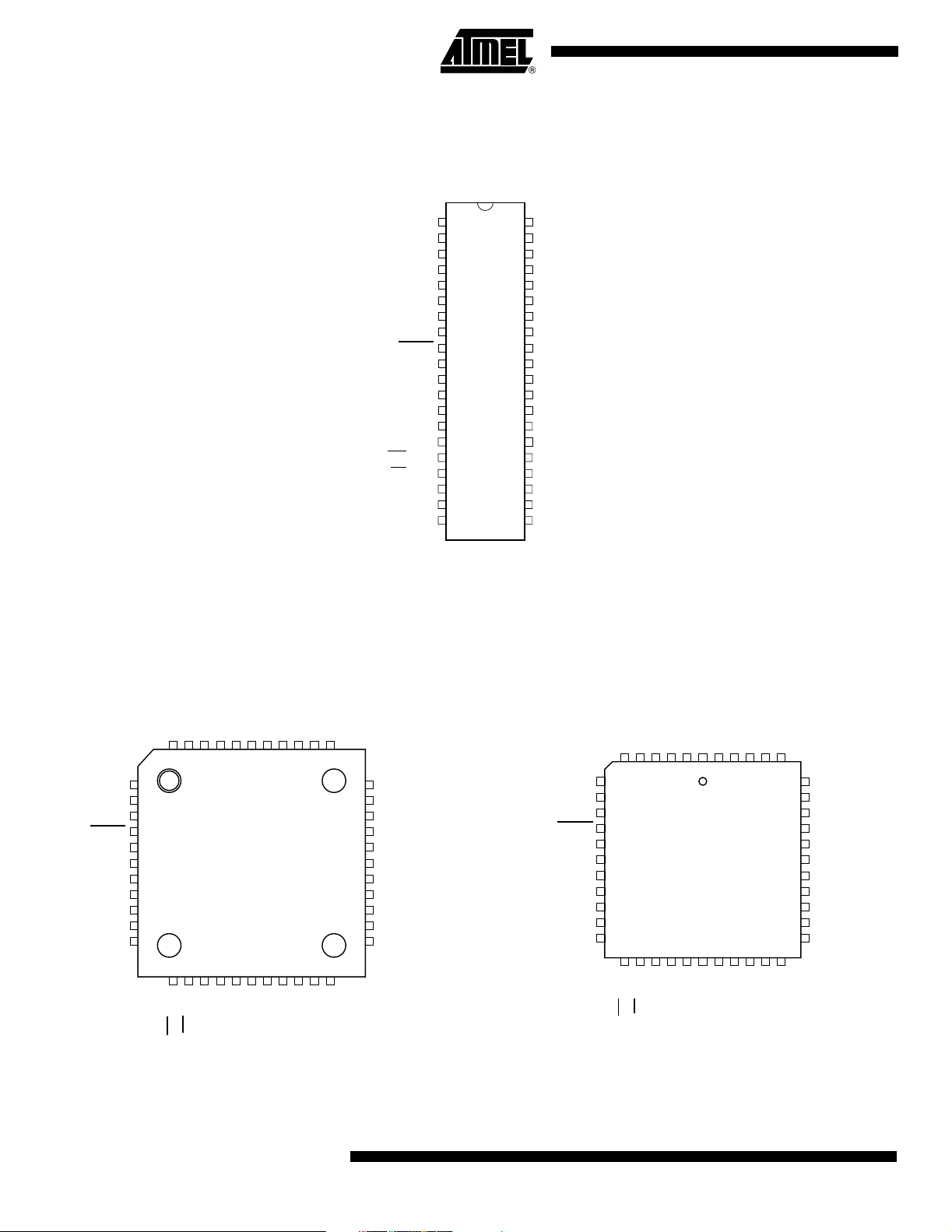
Figure 1. Pinout ATmega8515
PDIP
TQFP/MLF
(OC0/T0) PB0
(T1) PB1
(AIN0) PB2
(AIN1) PB3
(SS) PB4
(MOSI) PB5
(MISO) PB6
(SCK) PB7
RESET
(RXD) PD0
(TDX) PD1
(INT0) PD2
(INT1) PD3
(XCK) PD4
(OC1A) PD5
(WR) PD6
(RD) PD7
XTAL2
XTAL1
GND
1
2
3
4
5
6
7
8
9
10
11
12
13
14
15
16
17
18
19
20
40
VCC
39
PA0 (AD0)
38
PA1 (AD1)
37
PA2 (AD2)
36
PA3 (AD3)
35
PA4 (AD4)
34
PA5 (AD5)
33
PA6 (AD6)
32
PA7 (AD7)
31
PE0 (ICP/INT2)
30
PE1 (ALE)
29
PE2 (OC1B)
28
PC7 (A15)
27
PC6 (A14)
26
PC5 (A13)
25
PC4 (A12)
24
PC3 (A11)
23
PC2 (A10)
22
PC1 (A9)
21
PC0 (A8)
PLCC
(MOSI) PB5
(MISO) PB6
(SCK) PB7
RESET
(RXD) PD0
(TXD) PD1
(INT0) PD2
(INT1) PD3
(XCK) PD4
(OC1A) PD5
2
PB4 (SS)
PB3 (AIN1)
PB2 (AIN0)
PB1 (T1)
PB0 (OC0/T0)
NC*
VCC
4443424140393837363534
1
2
3
4
5
6
NC*
7
8
9
10
11
1213141516171819202122
NC*
GND
XTAL2
(RD) PD7
(WR) PD6
XTAL1
(A8) PC0
ATmega8515(L)
PA0 (AD0)
PA1 (AD1)
PA2 (AD2)
(A9) PC1
(A10) PC2
(A11) PC3
PA3 (AD3)
33
32
31
30
29
28
27
26
25
24
23
(A12) PC4
PA4 (AD4)
PA5 (AD5)
PA6 (AD6)
PA7 (AD7)
PE0 (ICP/INT2)
NC*
PE1 (ALE)
PE2 (OC1B)
PC7 (A15)
PC6 (A14)
PC5 (A13)
* NC= Do not connect
(May be used in future devices)
(MOSI) PB5
(MISO) PB6
(SCK) PB7
RESET
(RXD) PD0
NC*
(TXD) PD1
(INT0) PD2
(INT1) PD3
(XCK) PD4
(OC1A) PD5
PB4 (SS)
PB3 (AIN1)
PB2 (AIN0)
PB1 (T1)
PB0 (OC0/T0)
NC*
VCC
PA0 (AD0)
65432
7
8
9
10
11
12
13
14
15
16
17
1819202122232425262728
XTAL2
(RD) PD7
(WR) PD6
GND
XTAL1
1
4443424140
NC*
(A8) PC0
(A9) PC1
PA1 (AD1)
PA2 (AD2)
PA3 (AD3)
39
38
37
36
35
34
33
32
31
30
29
(A10) PC2
(A11) PC3
(A12) PC4
PA4 (AD4)
PA5 (AD5)
PA6 (AD6)
PA7 (AD7)
PE0 (ICP/INT2)
NC*
PE1 (ALE)
PE2 (OC1B)
PC7 (A15)
PC6 (A14)
PC5 (A13)
2512A–AVR–04/02
Page 3
ATmega8515(L)
Overview The ATmega8515 is a low-powerCMOS8-bit microcontrollerbas ed on theAVR
enhanced RISC architecture. By executing powerful instructions in a single clock cycle,
the ATmega8515 achieves throughputs approaching 1 MIPSperMHzallowing the sys-
tem designer to optimize powerconsumption versusprocessing speed.
Block Diagram Figure 2. Block Diagram
VCC
PA0 - PA7 PC0 - PC7
PORTA DRIVERS/BUFFERS
PE0 - PE2
PORTE
DRIVERS/
BUFFERS
PORTC DRIVERS/BUFFERS
GND
PORTA DIGITAL INTERFACE
PROGRAM
COUNTER
PROGRAM
FLASH
INSTRUCTION
REGISTER
INSTRUCTION
DECODER
CONTROL
LINES
AVR CPU
PROGRAMMING
LOGIC
STACK
POINTER
SRAM
GENERAL
PURPOSE
REGISTERS
X
Y
Z
ALU
STATUS
REGISTER
SPI
PORTE
DIGITAL
INTERFACE
PORTC DIGITAL INTERFACE
TIMERS/
COUNTERS
INTERNAL
OSCILLATOR
WATCHDOG
TIMER
MCU CTRL.
& TIMING
INTERRUPT
UNIT
EEPROM
USART
OSCILLATOR
INTERNAL
CALIBRATED
OSCILLATOR
XTAL1
XTAL2
RESET
2512A–AVR–04/02
+
-
PORTB DIGITAL INTERFACE
PORTB DRIVERS/BUFFERS
COMP.
INTERFACE
PORTD DIGITAL INTERFACE
PORTD DRIVERS/BUFFERS
PD0 - PD7PB0 - PB7
3
Page 4

TheAVRcore combines a rich instruction set with32 generalpurpose working registers.
All the 32 registers are directly connected to theArithmeticLogicUnit (ALU), allowing
twoindependent registers to beaccessed in one singleinstruction executed in one clock
cycle. The resulting architectureis more codeefficient whileachieving throughputs up to
ten timesfaster than conventionalCISCmicrocontrollers.
The ATmega8515 provides the following features: 8Kbytes ofIn-System Programmable
Flash with Read-While-Write capabilities, 512 bytesEEPROM, 512 bytesSRAM, an
External memory interface,35generalpurpose I/Olines, 32generalpurpose working
registers, two flexibleTimer/Counters withcomparemodes, Internal andExternal inter-
rupts, a Serial Programmable USART, a programmable Watchdog Timerwith internal
Oscillator, a SPIserialport, and three software selectable powersaving modes.The Idle
mode stops the CPUwhileallowing the SRAM, Timer/Counters, SPIport, andInterrupt
system to continue functioning. ThePower-downmode saves the Registercontentsbut
freezes the Oscillator, disabling all otherchipfunctions until thenextinterruptorhard-
ware reset. In Standby mode, the crystal/resonatorOscillator isrunning whilethe restof
th e deviceissleeping. This allows very fast start -upcombinedwithlow-power
consumption.
The deviceis manufactured using Atmel’shighdensity nonvolatilememory technology.
The On-chipISP Flash allows the program memory to be reprogrammedIn-System
through an SPIserial interface,bya conventional nonvolatilememory programmer, or
by an On-chipBoot program running on the AVR core. The boot program can useany
interfacetodownload theapplication program in theApplication Flash memory. Soft-
wareinthe Boot Flash section will continue to run whiletheApplication Flash section is
updated, providing true Read-While-Write operation. By combining an 8-bit RISC CPU
withIn-System Self-programmable Flash onamonolithicchip, theAtmel ATmega8515
is a powerful microcontroller that provides a highly flexibleandcosteffective solution to
many embeddedcontrol applications.
The ATmega8515 issupportedwith a full suite ofprogram andsystem development
tools including:CCompilers, Macroassemblers, Program debugger/simulators, In-cir-
cuit Emulators, andEvaluation kits.
Disclaimer Typical valuescontained in thisdata sheet are based on simulations andcharacteriza-
tion of other AVR microcontrollers manufactured on the same process technology. Min
andMax valueswill beavailableafter the deviceischaracterized.
AT90S4414/8515 and ATmega8515 Compatibility
AT90S4414/8515 Compatibility Mode
The ATmega8515 provides all the features of theAT90S4414/8515. Inaddition,several
newfeature s a readded .The ATmega8515 isba ckward comp atible with
AT90S4414/8515 in most cases. However, some incompatibilitiesbetween thetwo
microcontrollers exist. To solve thisproblem, an AT90S4414/8515 compatibility mode
can be selectedbyprogramming the S8515CFuse. ATmega8515 is 100%pin compatible with AT90S4414/8515, andcan replacetheAT90S4414/8515 on current printed
circuit boards. However, the location ofFuse bits and theelectricalcharacteristics differs between thetwo devices.
Programming the S8515CFuse will change the following functionality:
•Thetimedsequence forchanging the Watchdog Time-out period isdisabled. See
“TimedSequencesforChanging the Configuration of the Watchdog Timer”onpage
50 fordetails.
•The double buffering of the USART receive registers isdisabled. See “AVR USART
vs. AVR UART – Compatibility”onpage 133 fordetails.
•PORTE(2:1)will be set as output, and PORTE0 will be set as input.
4
ATmega8515(L)
2512A–AVR–04/02
Page 5

ATmega8515(L)
Pin Descriptions
VCC Digitalsupply voltage.
GND Ground.
Port A (PA7..PA0) PortAis an 8-bit bi-directionalI/Oport with internalpull-upresistors (selectedfor each
bit).ThePort A output buffers have symmetricaldrive characteristics withbothhighsink
andsource capability. When pins PA0toPA7 areused as inputs and areexternally
pulledlow, theywill source current if theinternalpull-upresistors areactivated.ThePort
A pins aretri-statedwhen a reset condition becomes active, even if the clock is not
running.
PortAalso serves the functions of variousspecialfeatures of the ATmega8515 aslisted
on page 64.
Port B (PB7..PB0) Port B is an 8-bit bi-directionalI/Oport with internalpull-upresistors (selectedfor each
bit).ThePort B output buffers have symmetricaldrive characteristics withbothhighsink
andsource capability.As inputs, Port Bpins that areexternally pulledlowwill source
current if the pull-upresistors areactivated.ThePort Bpins aretri-statedwhen a reset
condition becomes active, even if the clock is not running.
Port B also serves the functions of variousspecialfeatures of the ATmega8515 aslisted
on page 64.
Port C (PC7..PC0) Port C is an 8-bit bi-directionalI/Oport with internalpull-upresistors (selectedfor each
bit).ThePort C output buffers have symmetricaldrive characteristics withbothhighsink
andsource capability.As inputs, Port Cpins that areexternally pulledlowwill source
current if the pull-upresistors areactivated.ThePort Cpins aretri-statedwhen a reset
condition becomes active, even if the clock is not running.
Port D (PD7..PD0) Port D is an 8-bit bi-directionalI/Oport with internalpull-upresistors (selectedfor each
bit).ThePort D output buffers have symmetricaldrive characteristics withbothhighsink
andsource capability.As inputs, Port Dpins that areexternally pulledlowwill source
current if the pull-upresistors areactivated.ThePort Dpins aretri-statedwhen a reset
condition becomes active, even if the clock is not running.
Port D also serves the functions of variousspecialfeatures of the ATmega8515 aslisted
on page 69.
Port E(PE2..PE0) Port E is an 3-bit bi-directionalI/Oport with internalpull-upresistors (selectedfor each
bit).ThePort E output buffers have symmetricaldrive characteristics withbothhighsink
andsource capability.As inputs, Port Epins that areexternally pulledlowwill source
current if the pull-upresistors areactivated.ThePort Epins aretri-statedwhen a reset
condition becomes active, even if the clock is not running.
Port E also serves the functions of variousspecialfeatures of the ATmega8515 aslisted
on page 71.
RESET
XTA L1 Input to theinverting Oscillator amplifier and input to theinternalclock operating circuit.
XTA L2 Output from theinverting Oscillator amplifier.
2512A–AVR–04/02
Reset input. A lowlevel on thispin forlonger than the minimum pulse lengthwill gener-
ate a reset, even if the clock is not running. Theminimumpulse length is given in Table
18 on page 43. Shorterpulses are not guaranteed to generate a reset.
5
Page 6
About Code Examples
Thisdocumentation containssimple codeexamples that briefly showhow to usevarious
parts of the device. These codeexamples assume that the part specificheaderfileis
includedbefore compilation. Beawarethat not all C Compiler vendors include bit defini-
tions in the headerfiles and interrupt handling in C iscompilerdependent. Please
confirm with the CCompilerdocumentation for more details.
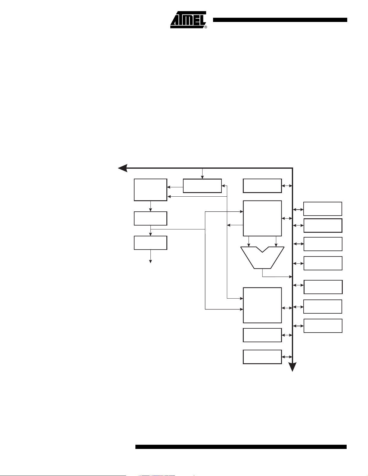
AVR CPU Cor e
Introduction Thissection discusses the AVR corearchitectureingeneral.Themainfunction of the
CPUcoreis to ensure correct program execution. The CPU musttherefore beableto
access memories, perform calculations, controlperipherals, andhandleinterrupts.
Architectural Overview Figure 3. Block Diagram of theAVRArchitecture
Data Bus 8-bit
Flash
Program
Memory
Instruction
Register
Instruction
Decoder
Control Lines
Program
Counter
Direct Addressing
Indirect Addressing
Status
and Control
32x8
General
Purpose
Registrers
ALU
Data
SRAM
EEPROM
Interrupt
Unit
SPI
Unit
Watchdog
Timer
Analog
Comparator
I/O Module1
I/O Module 2
I/O Module n
I/O Lines
Inorder to maximize performanceandparallelism, the AVR uses a Harvard architecture
– withseparate memories andbusesforprogram anddata. Instructions in the program
memory areexecutedwith a single levelpipelining. Whileoneinstruction isbeing exe-
cuted, thenextinstruction ispre-fetchedfrom the program memory.Thisconcept
enables instructions to beexecuted in every clock cycle. The program memory isIn-
System reprogrammable Flash memory.
6
ATmega8515(L)
2512A–AVR–04/02
Page 7

ATmega8515(L)
The fast-access RegisterFile contains32 x 8-bit generalpurpose working registers with
a single clock cycleaccess time. This allows single-cycleArithmeticLogicUnit (ALU)
operation. Inatypical ALU operation, twooperands areoutput from theRegisterFile,
theoperation is executed, and the resultisstoredback in the RegisterFile – in one
clock cycle.
Six of the 32 registers can beused as three 16-bit indirectaddress registerpointers for
Data Spaceaddressing – enabling efficient address calculations. One of thethese
address pointers can also beused as an address pointerforlook up tables in Flash pro-
gram memory.Theseaddedfunction registers arethe16-bit X-, Y-, andZ-register,
describedlater in thissection.
TheALU supports arithmetic andlogic operationsbetween registers orbetween a con-
stant and a register. Single register operationscan also beexecuted in theALU.After
an arithmetic operation, the Status Register is updated to reflectinformation about the
resultof theoperation.
Program flow isprovidedbyconditional and unconditionaljump andcall instructions,
abletodirectly address the wholeaddress space. Most AVR instructionshave a single
16-bit word format. Every program memory address contains a16- or32-bit instruction.
Program Flash memory spaceisdivided in two sections, the Boot Program section and
theApplication Program section. Bothsectionshave dedicatedLock bitsforwrite and
read/write protection. The SPM instruction that writes into theApplication Flash memory
section must resideinthe Boot Program section.
ALU – Arithmetic Logic Unit
During interrupts andsubroutine calls, the returnaddress program counter(PC) is
stored on the Stack.The Stack is effectively allocated in thegeneraldata SRAM, and
consequently the stack sizeis only limitedbythetotalSRAMsizeand theusage of the
SRAM.All userprograms mustinitializethe SPinthe reset routine (before subroutines
or interrupts areexecuted).The Stack PointerSPisread/write accessibleinthe I/O
space. The data SRAMcan easily beaccessed through the five different addressing
modessupported in the AVR architecture.
Thememory spaces in theAVRarchitectureareall linear andregular memory maps.
A flexibleinterruptmodule has itscontrolregisters in the I/Ospace with an additional
GlobalInterrupt Enable bit in the Status Register.All interruptshave a separate interrupt
vector in the InterruptVector table. Theinterruptshave priority in accordance with their
InterruptVectorposition. The lower the InterruptVector address, the higher the priority.
The I/O memory space contains64addressesforCPUperipheralfunctions asControl
Registers, SPI, and otherI/Ofunctions.The I/OMemory can beaccesseddirectly, or as
the Data Space locationsfollowing thoseof the RegisterFile,$20 -$5F.
The high-performance AVR ALU operates in direct connection with all the 32general
purpose working registers. Within a single clock cycle, arithmetic operationsbetween
generalpurpose registers orbetween a register and an immediate areexecuted.The
ALU operations are divided into three main categories –arithmetic, logical, andbit-func-
tions. Some implementations of thearchitecturealso provideapowerful multiplier
supporting bothsigned/unsigned multiplication andfractionalformat. See the“Instruc-
tion Set” section for a detaileddescription.
2512A–AVR–04/02
7
Page 8

Status Register The Status Registercontains information about the resultof themost recently executed
arithmetic instruction. This information can beusedfor altering program flow in order to
perform conditional operations. Note that the statusregister is updated after all ALU
operations, asspecified in the Instruction Set Reference. Thiswill in manycases
remove theneedfor using the dedicatedcompareinstructions, resulting in faster and
more compact code.
The statusregister is not automatically storedwhen enteringaninterrupt routine and
restoredwhen returning from an interrupt. This must be handledbysoftware.
TheAVRstatusregister – SREG –isdefined as:
Bit 76543 210
I THSVNZ CSREG
Read/Write R/W R/W R/W R/W R/W R/W R/W R/W
Initial Value00000000
• Bit 7 – I: Global Interrupt Enable
The GlobalInterrupt Enable bit must be set for theinterrupts to be enabled.Theindivid-
ual interrupt enable control is then performed in separate controlregisters. If theglobal
interruptenable register iscleared, none of theinterrupts areenabled independent of
theindividual interrupt enable settings.The I-bit isclearedbyhardwareafter an interrupt
has occurred, and isset by theRETI instruction to enable subsequent interrupts.The I-
bit can also be set andclearedbytheapplication with the SEI andCLIinstructions, as
described in theinstruction set reference.
• Bit 6 – T: Bit Copy Storage
The Bit Copy instructionsBLD(Bit LoaD) andBST (Bit STore) usetheT-bit assourceor
destination for theoperatedbit. A bit from a register in theRegisterFile can be copied
into T by the BSTinstruction, and a bit in T can be copied into a bit in a register in the
RegisterFile by the BLD instruction.
• Bit 5 – H: Half Carry Flag
The Half Carry Flag H indicates a half carry in some arithmetic operations. Half Carry is
useful in BCD arithmetic. See the“Instruction Set Description” fordetailed information.
• Bit 4 – S: Sign Bit, S = N
⊕ V
The S-bit is always an exclusive orbetween the negative flag N and thetwo’scomple-
ment overflowflag V. See the“Instruction Set Description” fordetailed information.
• Bit 3 – V: Two’s Complement Overflow Flag
TheTwo’sComplement OverflowFlag V supports two’scomplement arithmetics. See
the“Instruction Set Description” fordetailed information.
• Bit 2 – N: Negative Flag
The Negative Flag N indicates a negative resultinanarithmetic orlogic operation. See
the“Instruction Set Description” fordetailed information.
•Bit1–Z: Zero Flag
The Zero Flag Z indicates a zero resultinanarithmetic orlogic operation. See the
“Instruction Set Description” fordetailed information.
8
ATmega8515(L)
2512A–AVR–04/02
Page 9

ATmega8515(L)
• Bit0–C:CarryFlag
The Carry Flag C indicates a carry in an arithmetic orlogic operation. See the“Instruc-
tion Set Description” fordetailed information.
General Purpose Register File
TheRegisterFileis optimizedfor the AVR Enhanced RISC instruction set. Inorder to
achieve the requiredperformanceandflexibility, the following input/output schemes are
supportedbythe RegisterFile:
• One 8-bit output operand and one 8-bit resultinput
•Two8-bit output operands and one 8-bit resultinput
•Two8-bit output operands and one 16-bit resultinput
• One 16-bit output operand and one 16-bit resultinput
Figure4shows the structureof the 32 generalpurpose working registers in the CPU.
Figure 4. AVR CPUGeneral Purpose Working Registers
7 0Addr.
R0 $00
R1 $01
R2 $02
…
R13$0D
General R14 $0E
PurposeR15$0F
Working R16$10
Registers R17$11
…
R26$1A X-registerLowByte
R27$1BX-registerHighByte
R28 $1CY-registerLowByte
R29$1DY-registerHighByte
R30 $1EZ-registerLowByte
R31 $1FZ-registerHighByte
2512A–AVR–04/02
Mostof theinstructions operatingonthe RegisterFile have directaccess to all registers,
and mostof them are single cycleinstructions.
AsshowninFigure4, each register is alsoassigned a data memory address, mapping
them directly into the first 32 locations of theuserData Space. Although not being phys-
ically implemented asSRAMloc ations, this memory organization provides great
flexibility in access of the registers, as the X-, Y-, andZ-pointer Registers can be set to
index anyregister in the file.
9
Page 10
The X-register, Y-register, and Z-register
The registers R26..R31 have some addedfunctions to their generalpurposeusage.
These registers are16-bit address pointers for indirectaddressing of the Data Space.
Thethree indirectaddress registers X, Y, andZare defined asdescribed in Figure5.
Figure 5. The X-, Y-, andZ-registers
15 XH XL 0
X-register 7 0 7 0
R27($1B) R26($1A)
15 YH YL 0
Y-register 7 0 7 0
R29($1D) R28 ($1C)
15 ZH ZL 0
Z-register 7 0 7 0
R31 ($1F) R30 ($1E)
Inthe different addressing modes theseaddress registers have functions asfixeddis-
placement, automatic increment, and automaticdecrement (see the Instruction Set
reference fordetails).
Stack Pointer The Stack is mainly usedforstoring temporary data,forstoring local variables andfor
storing returnaddresses after interrupts andsubroutine calls.The Stack Pointer Regis-
ter always points to thetop of the stack. Note that the Stack is implemented as growing
from higher memory locations to lower memory locations.This implies that a stack
PUSH commanddecreases the Stack Pointer.
The Stack Pointerpoints to the data SRAMstack area wherethe Subroutine andInter-
rupt Stacks are located.ThisStack spaceinthe data SRAM must be definedbythe
program beforeanysubroutine calls areexecuted or interrupts areenabled.The Stack
Pointer must be set to point above $60. The Stack Pointer isdecrementedbyone when
data ispushed onto the Stack with thePUSH instruction, and it isdecrementedbytwo
when the returnaddress ispushed onto the Stack withsubroutine call or interrupt. The
Stack Pointer is incrementedbyone when data ispoppedfrom the Stack with thePOP
instruction, and it is incrementedbytwo when address ispoppedfrom the Stack with
return from subroutine RETorreturn from interruptRETI.
The AVR Stack Pointer is implemented as two8-bit registers in the I/Ospace. The num-
ber ofbits actually used is implementation dependent. Note that the data spaceinsome
implementations of theAVRarchitectureisso small that only SPL is needed. Inthis
case, the SPH Registerwill not be present.
Bit 15 14 13 12 11 10 9 8
SP15 SP14 SP13 SP12 SP11 SP10 SP9 SP8 SPH
SP7 SP6 SP5 SP4 SP3 SP2 SP1 SP0 SPL
76543 210
Read/Write R/W R/W R/W R/W R/W R/W R/W R/W
R/W R/W R/W R/W R/W R/W R/W R/W
Initial Value00000000
00000000
10
ATmega8515(L)
2512A–AVR–04/02
Page 11
ATmega8515(L)
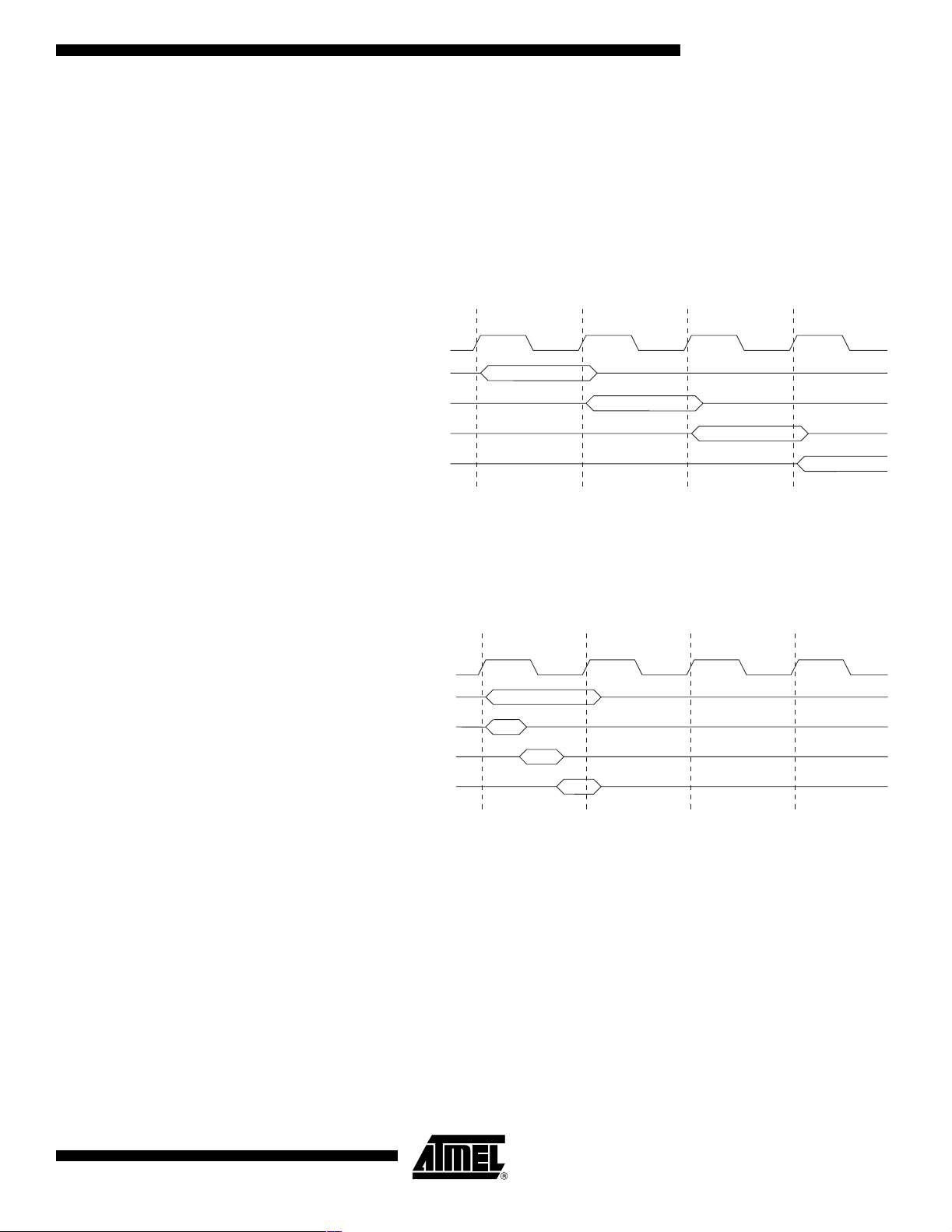
Instruction Execution Timing
Thissection describes the general access timing conceptsfor instruction execution. The
AVR CPU isdriven by the CPUclock clk
,directly generatedfrom the selectedclock
CPU
source for the chip. Nointernalclock division is used.
Figure 6shows the parallel instruction fetches and instruction executions enabledbythe
Harvard architectureand the fast-access Registerfile concept. This is the basicpipelin-
ing concepttoobtain up to 1 MIPSperMHzwith the corresponding unique resultsfor
functionspercost,functionsperclocks, andfunctionsperpower-unit.
Figure 6. TheParallelInstruction Fetches andInstruction Executions
T1 T2 T3 T4
clk
CPU
1st Instruction Fetch
1st Instruction Execute
2nd Instruction Fetch
2nd Instruction Execute
3rd Instruction Fetch
3rd Instruction Execute
4th Instruction Fetch
Figure 7shows theinternal timing concept for the Registerfile. Inasingle clock cyclean
ALU operation using two register operands is executed, and the resultisstoredback to
the destination register.
Reset and Interrupt Handling
Figure 7. Single CycleALU Operation
T1 T2 T3 T4
clk
CPU
Total Execution Time
Register Operands Fetch
ALU Operation Execute
Result Write Back
The AVR providesseveraldifferent interrupt sources.Theseinterrupts and the separate
Reset Vector each have a separate program vector in the program memory space. All
interrupts areassigned individual enable bitswhich must be written logic one together
with the GlobalInterrupt Enable bit in the Status Register in order to enabletheinterrupt.
Dependingonthe program counter value, interrupts maybe automatically disabled
when Boot Lock bitsBLB02 orBLB12 are programmed.Thisfeatureimprovessoftware
security. See the section “Memory Programming” on page 175 fordetails.
The lowestaddresses in the program memory spaceare by default defined as theReset
andInterruptVectors.The complete listof vectors isshownin“Interrupts”onpage 51.
The listalso determines the prioritylevels of the different interrupts.The lower the
address the higher is the prioritylevel.RESET has the highest priority, and nextisINT0
–the ExternalInterruptRequest0.The InterruptVectors can bemoved to the startof
the Boot Flash section by setting the IVSEL bit in the GeneralInterrupt Control Register
(GICR).Refer to “Interrupts”onpage 51 for moreinformation. TheReset Vectorcan
2512A–AVR–04/02
11
Page 12

also bemoved to the startof the Boot Flash section by programming the BOOTRST
Fuse,see “Boot LoaderSupport–Read-While-Write Self-Programming” on page 162.
When an interruptoccurs, the GlobalInterrupt Enable I-bit iscleared and all interrupts
are disabled.Theusersoftware can write logic one to the I-bit to enablenested inter-
rupts.All enabled interruptscan then interruptthe current interrupt routine. The I-bit is
automatically set whenaReturn from Interruptinstruction – RETI –is executed.
Thereare basically twotypes of interrupts.The firsttypeis triggeredbyan event that
sets theinterrupt flag. For theseinterrupts, theProgram Counter is vectored to the
actualInterruptVector in order to execute theinterrupt handling routine, andhardware
clears the corresponding interrupt flag. Interrupt flagscan also be clearedbywriting a
logic one to the flag bit position(s) to be cleared. If an interrupt condition occurs whilethe
corresponding Interrupt Enable bit iscleared, theinterrupt flag will be set andremembered until theinterruptis enabled, or the flag isclearedbysoftware. Similarly, if one or
moreinterrupt conditions occurwhilethe GlobalInterrupt Enable bit iscleared, the corresponding interrupt flag(s) will be set andremembered until the GlobalInterrupt Enable
bit isset, andwill then beexecutedbyorder ofpriority.
The second typeof interruptswill trigger aslong as theinterrupt condition ispresent.
Theseinterruptsdo not necessarily have interrupt flags. If theinterrupt condition disap-
pears beforetheinterruptis enabled, theinterrupt will not betriggered.
When the AVR exitsfrom an interrupt, it will always returntothemainprogram and exe-
cute one moreinstruction beforeanypending interruptisserved.
Note that the Status Register is not automatically storedwhen enteringaninterrupt rou-
tine, norrestoredwhen returning from an interrupt routine. This must be handledby
software.
When using the CLI instruction to disableinterrupts, theinterruptswill be immediately
disabled. Nointerrupt will beexecuted after the CLI instruction, even if it occurs simulta-
neously with the CLI instruction. The following example shows how thiscan beused to
avoid interruptsduring thetimedEEPROM write sequence..
Assembly Code Example
in r16, SREG
cli ; disable interrupts during timed sequence
sbi EECR, EEMWE
sbi EECR, EEWE
out SREG, r16
; store SREG value
; start EEPROM write
; restore SREG value (I-bit)
CCode Example
char cSREG;
cSREG = SREG;
/*
disable interrupts during timed sequence */
_CLI();
EECR |= (1<<EEMWE);
EECR |= (1<<EEWE);
SREG = cSREG;
/* store SREG value */
/* start EEPROM write */
/* restore SREG value (I-bit) */
12
ATmega8515(L)
2512A–AVR–04/02
Page 13

ATmega8515(L)
When using the SEI instruction to enableinterrupts, theinstruction following SEI will be
executedbeforeanypending interrupts, asshowninthis example.
Assembly Code Example
sei
; set global interrupt enable
sleep
; enter sleep, waiting for interrupt
; note: will enter sleep before any pending
; interrupt(s)
CCode Example
_SEI();
_SLEEP();
/* note: will enter sleep before any pending interrupt(s) */
Interrupt Response Time Theinterruptexecution response for all theenabled AVR interrupts isfourclock cycles
minimum. Afterfourclock cycles theProgram Vector address for theactual interrupt
handling routine is executed. During thisfourclock cycle period, theProgram Counter is
pushed onto the Stack.TheVector is normally a jump to theinterrupt routine, and this
jump takes three clock cycles. If an interruptoccurs during execution of amulti-cycle
instruction, this instruction iscompletedbeforetheinterruptisserved. If an interrupt
occurs when the MCU is in sleep mode, theinterruptexecution responsetimeis
increasedbyfourclock cycles.This increase comes in addition to the start-up time from
the selectedsleep mode.
/* set global interrupt enable */
/* enter sleep, waiting for interrupt */
A return from an interrupt handling routine takesfourclock cycles. During these four
clock cycles, theProgram Counter(two bytes) ispoppedback from the Stack, the Stack
Pointer is incrementedbytwo, and the I-bit in SREG isset.
2512A–AVR–04/02
13
Page 14

AVR ATmega8515 Memories
Thissection describes the different memories in the ATmega8515. The AVR architec-
ture has twomainmemory spaces, the Data Memory and theProgram Memory space.
Inaddition, the ATmega8515 features an EEPROM Memory fordata storage. All three
memory spaces are linear andregular.
In-System Reprogrammable Flash Program Memory
The ATmega8515 contains 8KbytesOn-chipIn-System Reprogrammable Flash memory forprogram storage. Sinceall AVR instructions are16 or32 bitswide, the Flash is
organized as 4Kx16. Forsoftware security, the Flash Program memory spaceis
divided into two sections, Boot Program section and Application Program section.
The Flash memory has an enduranceof at least1,000 write/erase cycles.Th e
ATmega8515 Program Counter(PC) is 12 bitswide, thus addressing the4Kprogram
memory locations.Theoperation ofBoot Program section and associatedBoot Lock
bitsforsoftware protection are described in detail in “Boot LoaderSupport–Read-
While-Write Self-Programming” on page 162. “Memory Programming” on page 175 con-
tains a detaileddescription on Flash data serialdownloading using the SPIpins.
Constant tablescan beallocatedwithin the entireProgram memory address space,see
the LPM – Load Program Memory instruction description.
Timing diagramsfor instruction fetch and execution are presented in “Instruction Execu-
tion Timing” on page 11.
Figure 8. Program Memory Map
$000
Application Flash Section
Boot Flash Section
$FFF
14
ATmega8515(L)
2512A–AVR–04/02
Page 15

ATmega8515(L)
SRAM Data Memory Figure 9shows how the ATmega8515 SRAMMemory is organized.
The lower608 Data Memory locations address theRegisterFile, the I/OMemory, and
theinternaldata SRAM.The first 96 locations address the RegisterFileandI/OMemory, and thenext 512 locations address theinternaldata SRAM.
An optional externaldata SRAMcan beusedwith the ATmega8515. ThisSRAMwill
occupy an area in the remaining address locations in the 64K address space. This area
starts at theaddress following theinternalSRAM.TheRegisterfile,I/O, ExtendedI/O
andInternalSRAM occupies the lowest 608 bytes in normal mode,so when using 64KB
(65536 bytes) ofExternalMemory, 64928 Bytes ofExternalMemory areavailable. See
“ExternalMemory Interface” on page 22 fordetails on how to takeadvantage of the
external memory map.
When theaddresses accessing the SRAM memory spaceexceeds theinternaldata
memory locations, theexternaldata SRAM is accessed using the same instructions as
for theinternaldata memory access. When theinternaldata memories areaccessed,
the read andwrite strobe pins(PD7 and PD6) areinactive during the wholeaccess
cycle. ExternalSRAM operation is enabledbysetting the SREbit in the MCUCR
register.
Accessing externalSRAM takes one additionalclock cycle perbyte compared to access
of theinternalSRAM.This means that the commands LD, ST,LDS,STS, LDD, STD,
PUSH, and POPtakeoneadditionalclock cycle. If the Stack isplaced in external
SRAM, interrupts, subroutine calls andreturns takethree clock cycles extra becausethe
two-byte program counter ispushed andpopped, and external memory access does not
takeadvantage of theinternalpipe-line memory access. When externalSRAM interface
is usedwithwait-state, one-byte external access takes two, three, orfour additional
clock cyclesfor one, two, and three wait-statesrespectively. Interrupts, subroutine calls
andreturnswill needfive,seven, or nine clock cycles morethan specified in theinstruction set manualfor one, two, and three wait-states.
The five different addressing modesfor the data memory cover: Direct,Indirect withDisplacement,Indirect,Indirect with Pre-decrement, andIndirect with Post-increment. In
the Registerfile,registers R26 to R31 featuretheindirectaddressing pointerregisters.
The directaddressing reaches theentire data space.
The Indirect withDisplacement mode reaches63address locationsfrom the base
address given by the Y- orZ-register.
When using register indirectaddressing modeswith automaticpre-decrement andpost-
increment, theaddress registers X, Y, andZare decremented or incremented.
The 32 generalpurpose working registers, 64 I/Oregisters, and the 512 bytes of internal
data SRAM in the ATmega8515 areall accessiblethrough all theseaddressing modes.
The Registerfileisdescribed in “General Purpose RegisterFile” on page 9.
2512A–AVR–04/02
15
Page 16
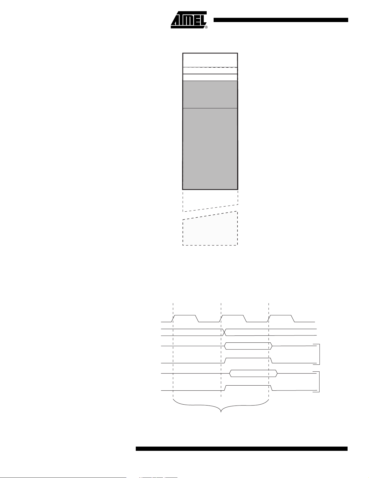
Figure 9. Data Memory Map
Data Memory
32 Registers
64 I/O Registers
Internal SRAM
(512 x 8)
External SRAM
(0 - 64K x 8)
$0000 - $001F
$0020 - $005F
$0060
$025F
$0260
$FFFF
Data Memory Access Times Thissection describes the general access timing conceptsfor internal memory access.
Theinternaldata SRAM access isperformed in two clk
cycles asdescribed in Figure
CPU
10.
Figure 10. On-chipData SRAM Access Cycles
T1 T2 T3
clk
CPU
Address
Compute Address
Address Valid
Data
WR
Write
Data
RD
Memory Access Instruction
Next Instruction
Read
16
ATmega8515(L)
2512A–AVR–04/02
Page 17
ATmega8515(L)
EEPROM Data Memory The ATmega8515 contains 512 bytes ofdata EEPROM memory. Itis organized as a
separate data space, in which single bytescan be read andwritten. The EEPROM has
an enduranceof at least100,000 write/erase cycles.Theaccess between the EEPROM
and the CPU isdescribed in the following,specifying the EEPROM Address Registers,
the EEPROM Data Register, and the EEPROM Control Register.
For a detaileddescription ofSPIdata downloading to the EEPROM, see page 189.
EEPROM Read/Write Access The EEPROM Access Registers areaccessibleinthe I/Ospace.
The write access time for the EEPROM is given in Table1.Aself-timing function,how-
ever, lets theusersoftware detect when thenext byte can be written. If theusercode
contains instructions that write the EEPROM, some precautions must betaken. In
heavily filteredpowersupplies, V
causes the device forsome period of time to run at a voltage lower than specified as
minimum for the clock frequency used. See “Preventing EEPROM Corruption” on page
21. fordetails on how to avoidproblems in these situations.
Inorder to prevent unintentionalEEPROM writes, a specificwrite proceduremust be fol-
lowed.Refer to the description of the EEPROM Control Registerfordetails on this.
When the EEPROM isread, the CPU ishaltedforfourclock cyclesbeforethenext
instruction is executed. When the EEPROM iswritten, the CPU ishaltedfor two clock
cyclesbeforethenextinstruction is executed.
islikely to riseorfall slowly on Power-up/down. This
CC
The EEPROM Address Register – EEARH and EEARL
The EEPROM Data Register – EEDR
Bit 15 14 13 12 11 10 9 8
–––––––EEAR8EEARH
EEAR7 EEAR6 EEAR5 EEAR4 EEAR3 EEAR2 EEAR1 EEAR0 EEARL
76543 210
Read/WriteRRRRRRRR/W
R/W R/W R/W R/W R/W R/W R/W R/W
Initial Value0000000X
XXXXXXXX
• Bits 15..9 – Res: Reserved Bits
These bits are reservedbits in the ATmega8515 andwill always read aszero.
• Bits 8..0 – EEAR8..0: EEPROM Address
The EEPROM Address Registers – EEARH andEEARL – specify the EEPROM
address in the512bytesEEPROM space. The EEPROM data bytes areaddressedlin-
early between0and 511. Theinitial value ofEEAR is undefined.Aproper value must be
written beforethe EEPROM maybeaccessed.
Bit 76543 210
MSB LSB EEDR
Read/Write R/W R/W R/W R/W R/W R/W R/W R/W
Initial Value00000000
2512A–AVR–04/02
• Bits 7..0 – EEDR7.0: EEPROM Data
For the EEPROM write operation, the EEDR Registercontains the data to be written to
the EEPROM in theaddress given by the EEAR Register. For the EEPROM read oper-
ation, the EEDR contains the data read out from the EEPROM at theaddress given by
EEAR.
17
Page 18

The EEPROM Control Register –EECR
Bit 76543 210
––––EERIEEEMWEEEWEEEREEECR
Read/WriteRRRRR/W R/W R/W R/W
Initial Value00000 0X 0
• Bits 7..4 – Res: Reserved Bits
These bits are reservedbits in the ATmega8515 andwill always read aszero.
• Bit 3 – EERIE: EEPROM Ready Interrupt Enable
Writing EERIE to one enables the EEPROM Ready Interruptif the I-bit in SREG isset.
Writing EERIE to zero disables theinterrupt. The EEPROM Ready interrupt generates a
constant interrupt when EEWE iscleared.
• Bit 2 – EEMWE: EEPROM Master Write Enable
The EEMWE bit determineswhethersetting EEWE to one causes the EEPROM to be
written. When EEMWE isset,setting EEWE within fourclock cycleswill write data to the
EEPROM at the selected address If EEMWE iszero,setting EEWE will have no effect.
When EEMWE hasbeen written to one by software,hardware clears the bit to zeroafter
fourclock cycles. See the description of the EEWE bit for an EEPROM write procedure.
• Bit 1 – EEWE: EEPROM Write Enable
The EEPROM Write Enable SignalEEWEis the write strobetothe EEPROM. When
address anddata are correctly set up, the EEWE bit must be written to one to write the
value into the EEPROM.The EEMWE bit must be written to one beforealogical one is
written to EEWE, otherwisenoEEPROM write takesplace. The following procedure
should be followedwhen writing the EEPROM (theorder ofsteps 3 and 4is not
essential):
1. Wait untilEEWEbecomeszero.
2. Wait untilSPMEN in SPMCR becomeszero.
3. Write newEEPROM address to EEAR (optional).
4. Write newEEPROM data to EEDR (optional).
5. Write a logical one to the EEMWE bit while writing a zerotoEEWE in EECR.
6. Within fourclock cycles aftersetting EEMWE, write a logical one to EEWE.
18
The EEPROM can not be programmedduring a CPUwritetothe Flash memory.The
softwaremust check that the Flash programming iscompletedbefore initiating a new
EEPROM write. Step 2is only relevant if the software contains a Boot Loader allowing
the CPU to program the Flash. If the Flash is neverbeing updatedbythe CPU, step 2
can be omitted. See “Boot LoaderSupport–Read-While-Write Self-Programming” on
page 162 fordetails about boot programming.
Caution: An interrupt between step 5andstep6will makethe write cycle fail, sincethe
EEPROM MasterWrite Enable will time-out. If an interrupt routine accessing the
EEPROM is interrupting anotherEEPROM access, the EEAR or EEDR Registerwill be
modified, causing theinterruptedEEPROM access to fail. Itisrecommended to have
theglobal interrupt flag clearedduring all the steps to avoid these problems.
When the write access time has elapsed, the EEWE bit isclearedbyhardware. The
usersoftware can poll thisbit andwait for a zero before writing thenext byte. When
EEWE hasbeen set, the CPU ishaltedfor two cyclesbeforethenextinstruction is
executed.
ATmega8515(L)
2512A–AVR–04/02
Page 19

ATmega8515(L)
• Bit 0 – EERE: EEPROM Read Enable
The EEPROM ReadEnable SignalEERE is the readstrobetothe EEPROM. When the
correctaddress isset up in the EEAR Register, the EEREbit must be written to a logic
one to trigger the EEPROM read.The EEPROM read access takes one instruction, and
the requesteddata is availableimmediately. When the EEPROM isread, the CPU is
haltedforfourcyclesbeforethenextinstruction is executed.
Theusershould poll the EEWE bit before starting the read operation. If a write operation
is in progress, it is neitherpossibletoread the EEPROM, nor to change the EEAR
Register.
The calibratedOscillator is used to time the EEPROM accesses.Table1lists thetypical
programming time forEEPROM access from the CPU.
Table 1. EEPROM Programming Time
Number of Calibrated RC
Symbol
EEPROM Write (from CPU) 8448 8.5 ms
Note: 1. Uses 1 MHz clock, independent of CKSEL Fuse settings.
Oscillator Cycles
(1)
Typ Programming Time
2512A–AVR–04/02
19
Page 20

The following codeexamplesshow one assembly and one Cfunction forwriting to the
EEPROM.Theexamples assume that interrupts are controlled(e.g.,bydisabling inter-
rupts globally) sothat no interruptswill occurduring execution of these functions.The
examples alsoassume that no Flash Boot Loader ispresent in the software. If such
codeispresent, the EEPROM write function mustalso wait for any ongoing SPMcom-
mand to finish.
Assembly Code Example
EEPROM_write:
; Wait for completion of previous write
sbic EECR,EEWE
rjmp EEPROM_write
; Set up address (r18:r17) in address register
out EEARH, r18
out EEARL, r17
; Write data (r16) to data register
out EEDR,r16
; Write logical one to EEMWE
sbi EECR,EEMWE
; Start eeprom write by setting EEWE
sbi EECR,EEWE
ret
CCode Example
void EEPROM_write(unsigned int uiAddress, unsigned char ucData)
{
Wait for completion of previous write
/*
while(EECR & (1<<EEWE))
;
/* Set up address and data registers */
EEAR = uiAddress;
EEDR = ucData;
Write logical one to EEMWE */
/*
EECR |= (1<<EEMWE);
/* Start eeprom write by setting EEWE */
EECR |= (1<<EEWE);
}
*/
20
ATmega8515(L)
2512A–AVR–04/02
Page 21

ATmega8515(L)
Thenext codeexamplesshow assembly andCfunctionsforreading the EEPROM.The
examples assume that interrupts are controlledsothat no interruptswill occurduring
execution of these functions.
Assembly Code Example
EEPROM_read:
; Wait for completion of previous write
sbic EECR,EEWE
rjmp EEPROM_read
; Set up address (r18:r17) in address register
out EEARH, r18
out EEARL, r17
; Start eeprom read by writing EERE
sbi EECR,EERE
; Read data from data register
in r16,EEDR
ret
CCode Example
unsigned char EEPROM_read(unsigned int uiAddress)
{
/* Wait for completion of previous write */
while(EECR & (1<<EEWE))
;
/* Set up address register */
EEAR = uiAddress;
Start eeprom read by writing EERE */
/*
EECR |= (1<<EERE);
/* Return data from data register */
return EEDR;
}
Preventing EEPROM Corruption
2512A–AVR–04/02
During periods oflow V
, the EEPROM data can be corruptedbecausethe supply volt-
CC
age is too lowfor the CPU and the EEPROM to operate properly.Theseissues arethe
same asforboard levelsystems using EEPROM, and the same design solutionsshould
beapplied.
An EEPROM data corruption can be causedbytwo situationswhen thevoltage is too
low. First, a regularwrite sequencetothe EEPROM requires aminimumvoltage to
operate correctly. Secondly, the CPU itself can execute instructions incorrectly, if the
supply voltage is too low.
EEPROM data c o rruption c an easi ly beavoid edbyfo llo wing th isdes ign
recommendation:
Keep the AVR RESETactive (low) during periods of insufficient powersupply volt-
age. Thiscan be done by enabling theinternalBrown-out Detector(BOD). If the
detection level of theinternalBODdoes not match theneededdetection level, an
externallow V
Reset Protection circuit can beused. If aReset occurs whilea
CC
write operation is in progress, the write operation will be completedprovided that the
powersupply voltage issufficient.
21
Page 22

I/O Memory The I/Ospace definition of the ATmega8515 isshown in “RegisterSummary”onpage
209.
All ATmega8515 I/Os andperipherals are placed in the I/Ospace. The I/Olocations are
accessedbythe IN andOUTinstructions, transferring data between the 32 generalpur-
pose working registers and the I/Ospace. I/O Registers within theaddress range $00 -
$1F are directly bit-accessibleusing the SBI andCBIinstructions. Inthese registers, the
value ofsingle bitscan be checkedbyusing the SBIS andSBICinstructions.Refer to
theinstruction set section for more details. When using the I/Ospecificcommands IN
andOUT, the I/O addresses$00 -$3Fmust beused. When addressing I/O Registers as
data spaceusing LD andSTinstructions, $20 must beadded to theseaddresses.
Forcompatibilitywithfuture devices, reservedbitsshould be written to zeroif accessed.
ReservedI/O memory addressesshould neverbe written.
Some of the statusflags are clearedbywriting a logical one to them. Note that the CBI
and SBI instructionswill operate on all bits in the I/O Register, writing a one back into
anyflag read asset, thusclearing the flag. The CBI andSBIinstructionswork withreg-
isters $00 to $1F only.
The I/O andperipherals controlregisters areexplained in latersections.
External Memory Interface
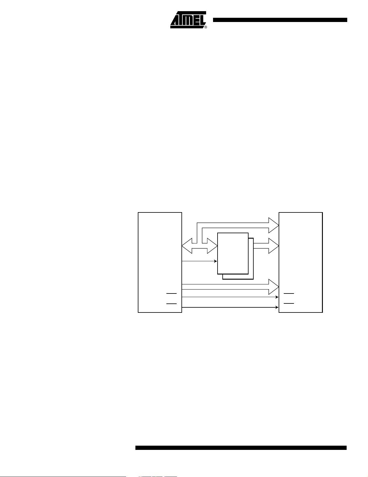
Overview When theeXternalMEMory (XMEM) is enabled, address space outsidetheinternal
With all the features the ExternalMemory Interface provides, it iswell suited to operate
as an interfacetomemory devicessuch as externalSRAM andFlash, andperipherals
such as LCD-display, A/D, andD/A. Themainfeatures are:
•
Four Different Wait State Settings (Including No wait State)
• Independent Wait State Setting for Different External Memory Sectors (Configurable
Sector Size)
• The Number of Bits Dedicated to Address High Byte is Selectable
• Bus Keepers on Data Lines to Minimize Current Consumption (Optional)
SRAMbecomes availableusing the dedicated external memory pins(see Figure1on
page 2, Table26 on page 63, Table 32onpage 67, and Table 38onpage 71).The
memory configuration isshowninFigure11.
22
ATmega8515(L)
2512A–AVR–04/02
Page 23
Figure 11. ExternalMemory withSectorSelect
Internal Memory
Lower Sector
SRW01
SRW00
ATmega8515(L)
0x0000
0x25F
0x260
SRL[2..0]
Using the External Memory Interface
External Memory
(0-64K x 8)
Theinterface consists of:
•AD7:0:Multiplexedlow-order address bus anddata bus
•A15:8:High-order address bus(configurable number ofbits)
•ALE: Address latch enable
•RD
• WR
The controlbitsfor the ExternalMemory Interfaceare located in three registers, the
MCU Control Register – MCUCR, the ExtendedMCUControl Register – EMCUCR, and
the SpecialFunction IO Register – SFIOR.
: Readstrobe
:Write strobe
Upper Sector
SRW11
SRW10
0xFFFF
2512A–AVR–04/02
When the XMEM interfaceis enabled, it will overridethe settings in the data direction
registers correspondingtothe portsdedicated to theinterface. Fordetails about thisport
override,see thealternate functions in section “I/O Ports”onpage 56.The XMEM inter-
face will auto-detect whether an access is internal or external. If theaccess is external,
the XMEM interface will output address, data, and the controlsignals on the ports
according to Figure13(thisfigure shows the wave formswithout wait states). When
ALE goesfrom high to low, thereis avalid address on AD7:0. ALE islowduring a data
transfer. When the XMEM interfaceis enabled, alsoaninternal access will causeactivity on address-, data-, and ALE ports, but theRD
internal access. When the ExternalMemory Interfaceisdisabled, thenormalpin and
andWR strobeswill not toggle during
23
Page 24
data direction settings areused. Note that when the XMEM interfaceisdisabled, the
address spaceabove theinternalSRAMboundary is not mapped into theinternal
SRAM. Figure12illustrateshow to connectanexternalSRAM to the AVR using an octal
latch (typically “74x573”or equivalent)which is transparent when G ishigh.
Address Latch Requirements Due to the high-speed operation of the XRAM interface, theaddress latch must be
selectedwithcare for system frequencies above 8 MHz @ 4V and 4 MHz @ 2.7V.
When operating at conditions above these frequencies, thetypical old style 74HC series
latch becomes inadequate. Theexternal memory interfaceisdesigned in complianceto
the 74AHC serieslatch. However, most latchescan beused aslong theycomply with
themaintimingparameters.Themainparameters for theaddress latch are:
• D to Qpropagation delay(t
• Data setup time before Glow(t
• Data (address) hold time afterGlow(
Theexternal memory interfaceisdesigned to guaranty minimum address hold time after
G is assertedlow of t
201).The D to Qpropagation delay(t
ing theaccess time requirement of theexternalcomponent. The data setup time before
Glow(t
(dependent on the capacitive load).
Figure 12. ExternalSRAMConnected to the AVR
) mustnotexceed address valid to ALE low(t
su
= 5ns(refer to t
h
pd
)
)
su
)
th
LAXX_LD/tLLAXX_ST
) must betaken into consideration when calculat-
pd
in Table 99 to Table106 on page
) minus PCB wiring delay
AVLLC
D[7:0]
AD7:0
ALE
DQ
G
A[7:0]
SRAM
AVR
A15:8
RD
WR
Pull-up and Bus Keeper The pull-upresistors on theAD7:0 ports maybeactivated if the corresponding Port reg-
ister iswritten to one. To reduce powerconsumption in sleep mode, it isrecommended
to disablethe pull-ups by writing thePort register to zero before entering sleep.
The XMEM interfacealso provides a buskeeper on theAD7:0 lines.The buskeeper
can be disabled and enabled in softwareasdescribed in “SpecialFunction IO Register –
SFIOR” on page 29. When enabled, the buskeeperwill keep the previous value on the
AD7:0 buswhilethese lines aretri-statedbythe XMEM interface.
If neitherbus-keeper norpull-ups are enabled, the XMEM interface will leave theAD7:0
tri-statedduring a read access until thenextRAM access (internal or external) appears.
A[15:8]
RD
WR
Timing External memory deviceshave various timing requirements. To meet these require-
ments, the ATmega8515 XMEM interface providesfourdifferent wait states asshownin
Table 3. Itis important to consider thetimingspecification of theexternal memory
device before selecting the wait state. Themostimportant parameters aretheaccess
24
ATmega8515(L)
2512A–AVR–04/02
Page 25
ATmega8515(L)
time for theexternal memory in conjunction with the set-upreq uirement of the
ATmega8515. Theaccess time for theexternal memory isdefined to bethetimefrom
receiving the chipselect/address until the data of this address actually isdriven on the
bus.Theaccess time cannot exceed thetimefrom theALE pulseis assertedlow until
data must be stable during a readsequence (t
106 on page 201).The different wait states are set up in software. As an additionalfeature, it ispossibletodividetheexternal memory spaceintwo sectors with individualwait
state settings.This makes it possibletoconnecttwo different memory deviceswithdif-
ferent timing requirements to the same XMEM interface. ForXMEMinterface timing
details, please refer to Figure89 to Figure 92, and Table 99 to Table106.
Note that the XMEM interfaceis asynchronous and that the waveforms in the figures
below are related to theinternal system clock.The skewbetween the Internal andExter-
nalclock (XTAL1) is not guaranteed(it variesbetween devices, temperature, andsupply
voltage). Consequently, the XMEM interfaceis not suitedforsynchronous operation.
LLRL
+ t
RLRH
- t
in Table 99 to Table
DVRH
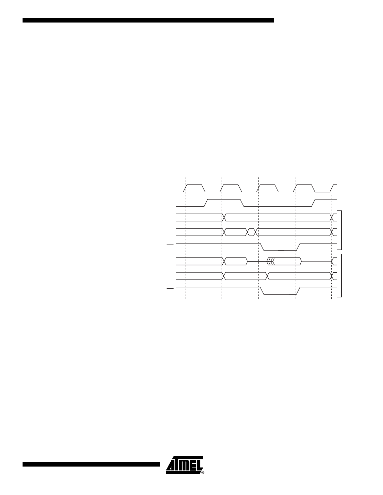
Figure 13. ExternalData Memory Cycle swithout Wait State (SRW n1 = 0and
SRWn0 = 0)
System Clock (CLK
(1)
CPU
ALE
A15:8
DA7:0
WR
DA7:0 (XMBK = 0)
DA7:0 (XMBK = 1)
RD
T1 T2 T3
)
AddressPrev. Addr.
Address DataPrev. Data XX
DataPrev. Data Address
DataPrev. Data Address
T4
Write
Read
Note: 1. SRWn1 =SRW11 (uppersector) orSRW01 (lowersector), SRWn0 =SRW10 (upper
sector) orSRW00 (lowersector)
TheALE pulseinperiod T4 is only present if thenextinstruction accesses theRAM
(internal or external).
2512A–AVR–04/02
25
Page 26
Figure 14. ExternalData Memory CycleswithSRWn1 = 0andSRWn0 = 1
System Clock (CLK
CPU
ALE
T1 T2 T3
)
T4
(1)
T5
A15:8
DA7:0
WR
DA7:0 (XMBK = 0)
DA7:0 (XMBK = 1)
RD
Address DataPrev. Data XX
AddressPrev. Addr.
DataPrev. Data Address
DataPrev. Data Address
Note: 1. SRWn1 =SRW11 (uppersector) orSRW01 (lowersector), SRWn0 =SRW10 (upper
sector) orSRW00 (lowersector)
TheALE pulseinperiod T5 is only present if thenextinstruction accesses theRAM
(internal or external).
Figure 15. ExternalData Memory CycleswithSRWn1 = 1andSRWn0 = 0
System Clock (CLK
CPU
ALE
A15:8
DA7:0
T1 T2 T3
)
AddressPrev. Addr.
Address DataPrev. Data XX
T4 T5
(1)
T6
Write
Read
Write
WR
DA7:0 (XMBK = 0)
DA7:0 (XMBK = 1)
RD
DataPrev. Data Address
DataPrev. Data Address
Note: 1. SRWn1 =SRW11 (uppersector) orSRW01 (lowersector), SRWn0 =SRW10 (upper
sector) orSRW00 (lowersector)
TheALE pulseinperiod T6 is only present if thenextinstruction accesses theRAM
(internal or external).
Read
26
ATmega8515(L)
2512A–AVR–04/02
Page 27
ATmega8515(L)
XMEM Register Description
MCU Control Register – MCUCR
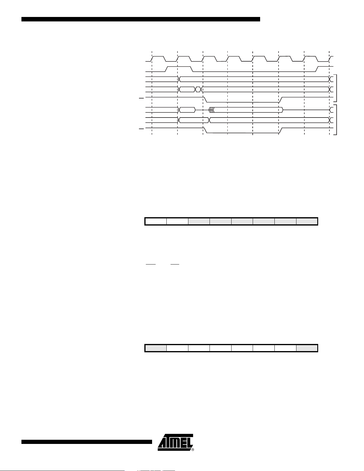
Figure 16. ExternalData Memory CycleswithSRWn1 = 1andSRWn0 = 1
System Clock (CLK
DA7:0 (XMBK = 0)
DA7:0 (XMBK = 1)
CPU
ALE
A15:8
DA7:0
WR
)
T1 T2 T3
AddressPrev. Addr.
Address DataPrev. Data XX
DataPrev. Data Address
DataPrev. Data Address
RD
T4 T5 T6
(1)
T7
Note: 1. SRWn1 =SRW11 (uppersector) orSRW01 (lowersector), SRWn0 =SRW10 (upper
sector) orSRW00 (lowersector)
TheALE pulseinperiod T7 is only present if thenextinstruction accesses theRAM
(internal or external).
Bit 76543 210
SRE SRW10
Read/Write R/W R/W R/W R/W R/W R/W R/W R/W
Initial Value00000000
SE SM1 ISC11 ISC10 ISC01 ISC00 MCUCR
Write
Read
Extended MCU Control Register – EMCUCR
• Bit 7 – SRE: External SRAM/XMEM Enable
Writing SRE to one enables the ExternalMemory Interface.The pin functions AD7:0,
A15:8, ALE, WR
, and RD areactivated as thealternate pin functions.The SREbit over-
rides anypin direction settings in the respective Data Direction Registers. Writing SRE
to zero,disables the ExternalMemory Interfaceand thenormalpin anddata direction
settings areused.
• Bit 6 – SRW10: Wait State Select Bit
For a detaileddescription,see common description for the SRWn bitsbelow (EMCUCR
description).
Bit 76543 210
SM0 SRL2 SRL1 SRL0 SRW01 SRW00 SRW11 ISC2 EMCUCR
Read/Write R/W R/W R/W R/W R/W R/W R/W R/W
Initial Value00000000
• Bit 6..4 – SRL2, SRL1, SRL0: Wait State Sector Limit
Itispossibletoconfigure different wait statesfordifferent external memory addresses.
The ExternalMemory address space can be divided in two sectors that have separate
wait state bits.The SRL2,SRL1, andSRL0 bitsselectthe splitting of these sectors, see
Table2andFigure11.By default, the SRL2,SRL1, andSRL0 bits are set to zeroand
theentire ExternalMemory address spaceis treated as one sector. When the entire
2512A–AVR–04/02
27
Page 28

SRAM address spaceisconfigured as one sector, the wait states are configuredbythe
SRW11 andSRW10 bits.
Table 2. SectorLimitswithDifferent Settings ofSRL2..0
SRL2 SRL1 SRL0 Sector Limits
000
001
010
011
100
101
110
111
Lowersector=N/A
Uppersector=0x0260 - 0xFFFF
Lowersector=0x0260 - 0x1FFF
Uppersector=0x2000 - 0xFFFF
Lowersector=0x0260 - 0x3FFF
Uppersector=0x4000 - 0xFFFF
Lowersector=0x0260 - 0x5FFF
Uppersector=0x6000 - 0xFFFF
Lowersector=0x0260 - 0x7FFF
Uppersector=0x8000 - 0xFFFF
Lowersector=0x0260 - 0x9FFF
Uppersector=0xA000 - 0xFFFF
Lowersector=0x0260 - 0xBFFF
Uppersector=0xC000 - 0xFFFF
Lowersector=0x0260 - 0xDFFF
Uppersector=0xE000 - 0xFFFF
• Bit 1 and Bit 6 MCUCR – SRW11, SRW10: Wait State Select Bits for Upper
Sector
The SRW11 andSRW10 bitscontrol thenumber ofwait statesfor theuppersector of
the ExternalMemory address space,see Table 3.
• Bit 3..2 – SRW01, SRW00: Wait State Select Bits for Lower Sector
The SRW01 andSRW00 bitscontrol thenumber ofwait statesfor the lowersector of
the ExternalMemory address space,see Table 3.
Table 3. Wait States
SRWn1 SRWn0 Wait States
00No wait states.
01Wait one cycle during read/write strobe.
10Wait two cyclesduring read/write strobe.
11
Note: 1. n = 0or 1 (lower/uppersector).
Forfurtherdetails of thetimingandwait states of the ExternalMemory Interface,see
Figure13 to Figure16how the setting of the SRWbits affects the timing.
(1)
Wait two cyclesduring read/write andwait one cycle before driving out
new address.
28
ATmega8515(L)
2512A–AVR–04/02
Page 29

ATmega8515(L)
Special Function IO Register – SFIOR
Bit 76543 210
– XMBK XMM2 XMM1 XMM0 PUD – PSR10 SFIOR
Read/Write R/W R/W R/W R/W R/W R/W R/W R/W
Initial Value000000 00
•Bit6–XMBK: External Memory Bus Keeper Enable
Writing XMBK to one enables the BusKeeper on theAD7:0 lines. When the BusKeeper
is enabled, AD7:0 will keep the last driven value on the lines even if the XMEM interface
has tri-stated the lines. Writing XMBK to zero disables the BusKeeper. XMBK is not
qualifiedwithSRE, soevenif the XMEM interfaceisdisabled, the BusKeepers are still
activated aslong asXMBKis one.
• Bit 6..3 – XMM2, XMM1, XMM0: External Memory High Mask
When the ExternalMemory is enabled, all Port Cpins areusedfor the high address
byte by default. If the full 60KB address spaceis not required to access the External
Memory, some, or all, Port Cpinscan be releasedfor normal PortPinfunction as
described in Table4.Asdescribed in “Using all 64KB Locations ofExternalMemory”on
page 30, it ispossibletousethe XMMn bits to access all 64KB locations of the External
Memory.
Table 4. Port C Pins Released asNormal PortPinswhen the ExternalMemory is
Enabled
XMM2 XMM1 XMM0 # Bits for External Memory Address Released Port Pins
0008(Full 60 KB space)None
0017 PC7
0106 PC7 - PC6
0115 PC7 - PC5
1004 PC7 - PC4
1013 PC7 - PC3
1102 PC7 - PC2
111NoAddress HighbitsFull Port C
2512A–AVR–04/02
29
Page 30

Using all 64KB Locations of External Memory
Sincethe ExternalMemory is mapped after the InternalMemory asshowninFigure11,
only 60KB ofExternalMemory is available by default (address space0x0000 to 0x025F
isreservedforInternalMemory). However, it ispossibletotakeadvantage of the entire
ExternalMemory by masking the higher address bits to zero. Thiscan be done by using
the XMMn bits andcontrolbysoftwarethemost significant bits of theaddress. By setting Port C to output 0x00, andreleasing themost significant bitsfor normal PortPin
operation, the Memory Interface will address 0x0000 - 0x1FFF. See codeexample
below.
Assembly Code Example
; OFFSET is defined to 0x2000 to ensure
; external memory access
; Configure Port C (address high byte) to
; output 0x00 when the pins are released
; for normal Port Pin operation
ldi r16, 0xFF
out DDRC, r16
ldi r16, 0x00
out PORTC, r16
; release PC7:5
ldi r16, (1<<XMM1)|(1<<XMM0)
out SFIOR, r16
; write 0xAA to address 0x0001 of external
; memory
ldi r16, 0xaa
sts 0x0001+OFFSET, r16
; re-enable PC7:5 for external memory
ldi r16, (0<<XMM1)|(0<<XMM0)
out SFIOR, r16
; store 0x55 to address (OFFSET + 1) of
; external memory
ldi r16, 0x55
sts 0x0001+OFFSET, r16
CCode Example
#define OFFSET 0x2000
(1)
(1)
30
void XRAM_example(void)
{
unsigned char *p = (unsigned char *) (OFFSET + 1);
DDRC = 0xFF;
PORTC = 0x00;
SFIOR = (1<<XMM1) | (1<<XMM0);
*p = 0xaa;
SFIOR = 0x00;
*p = 0x55;
}
Note: 1. Theexample codeassumes that the part specificheaderfileis included.
Caremust beexercised using this option as mostof thememory is masked away.
ATmega8515(L)
2512A–AVR–04/02
Page 31

System Clock and Clock Options
ATmega8515(L)
Clock Systems and their Distribution
Figure17presents the principalclock systems in the AVR and theirdistribution. All of
the clocks need not beactive at a given time. Inorder to reduce powerconsumption, the
clocks to modules not being usedcan be haltedbyusing different sleep modes, as
described in “PowerManagement andSleepModes”onpage 38. The clock systems
are detailedbelow.
Figure 17. Clock Distribution
General I/O
Modules
clk
I/O
AVR Clock
Control Unit
CPU Core RAM
clk
CPU
clk
FLASH
Reset Logic
Watchdog Timer
Flash and
EEPROM
CPU Clock – clk
I/O Clock – clk
I/O
CPU
External RC
Oscillator
Source clock
Clock
Multiplexer
External Clock
Crystal
Oscillator
Watchdog clock
Watchdog
Low-frequency
Crystal Oscillator
Oscillator
Calibrated RC
Oscillator
The CPUclock isrouted to parts of the system concernedwith operation of theAVR
core. Examples ofsuch modules arethe General PurposeRegisterFile, the Status Reg-
ister, and the data memory holding the Stack Pointer. Halting the CPUclock inhibits the
core from performing general operations andcalculations.
The I/Oclock is usedbythemajority of the I/O modules, likeTimer/Counters, SPI, and
USART. The I/Oclock is alsousedbythe ExternalInterruptmodule,but note that some
external interrupts are detectedbyasynchronouslogic, allowing such interrupts to be
detected even if the I/Oclock ishalted.
2512A–AVR–04/02
31
Page 32

Flash Clock – clk
FLASH
The Flash clock controls operation of the Flash interface. The Flash clock is usually
active simultaneously with the CPUclock.
Clock Sources The device has the following clock sourceoptions, selectable by Flash Fuse bits as
shown below.The clock from the selectedsourceis input to the AVR clock generator,
androuted to theappropriate modules.
Table 5. Device Clocking OptionsSelect
Device Clocking Option CKSEL3..0
ExternalCrystal/Ceramic Resonator 1111 - 1010
ExternalLow-frequency Crystal 1001
External RCOscillator 1000 - 0101
CalibratedInternal RCOscillator 0100 - 0001
ExternalClock 0000
Note: 1. For all fuses “1” means unprogrammedwhile“0”meansprogrammed.
(1)
Thevariouschoicesfor each clocking option is giveninthe following sections. When the
CPUwakes upfrom Power-downor Power-save, the selectedclock sourceis used to
time the start-up, ensuring stable Oscillator operation beforeinstruction execution starts.
When the CPUstartsfrom Reset, thereis as an additionaldelay allowing the power to
reach a stable levelbefore commencing normal operation. The Watchdog Oscillator is
usedfor timing thisreal-time partof the start-up time. Thenumber ofWDT Oscillator
cycles usedfor each time-out isshowninTable 6.The frequency of the Watchdog Oscillator is voltage dependent asshown in “ATmega8515 TypicalCharacteri stics –
Preliminary Data” on page 204. The deviceisshippedwith CKSEL = “0001” and
SUT = “10” (1 MHz Internal RCOscillator, slowly rising power).
Table 6. Number ofWatchdog Oscillator Cycles
Typ Time-out (VCC= 5.0V) Typ Time-out (VCC= 3.0V) Number of Cycles
4.1 ms 4.3 ms 4K(4,096)
65ms69ms64K65,536)
Crystal Oscillator XTAL1andXTAL2areinput and output,respectively, of an inverting amplifierwhich can
be configuredfor useas an On-chipOscillator, asshowninFigure18.Either a quartz
crystal or a ceramicresonator maybeused.The CKOPT Fuse selectsbetween two different oscillator amplifier modes. When CKOPT isprogrammed, the Oscillator output
will oscillate will a full rail-to-railswingontheoutput. This modeissuitable when operatinginavery noisy environment orwhen theoutput from XTAL2 drives a secondclock
buffer.This mode has a wide frequency range. When CKOPT is unprogrammed, the
Oscillatorhas a smaller output swing. Thisreducespowerconsumption considerably.
This mode has a limitedfrequency range and it can not beused to drive otherclock
buffers.
Forresonators, themaximum frequency is 8 MHz withCKOPT unprogrammed and
16MHzwithCKOPT programmed. C1andC2 should always beequalforbothcrystals
andresonators.Theoptimal value of the capacitors depends on the crystal orresonator
in use, theamountofstraycapacitance, and theelectromagnetic noiseof theenviron-
ment. Some initial guidelinesforchoosing capacitors for use withcrystals aregivenin
Table 7. Forceramicresonators, the capacitor values given by the manufacturershould
beused.
32
ATmega8515(L)
2512A–AVR–04/02
Page 33

Figure 18. CrystalOscillatorConnections
ATmega8515(L)
C2
C1
XTAL2
XTAL1
GND
The Oscillatorcan operateinthree different modes, each optimizedfor a specificfre-
quency range. Theoperating modeisselectedbythe fuses CKSEL3..1 asshownin
Table 7.
Table 7. CrystalOscillatorOperating Modes
Frequency Range
CKOPT CKSEL3..1
1 101
1 110 0.9-3.0 12 - 22
1 111 3.0 - 8.0 12 - 22
0101, 110, 111 1.0 - 12 - 22
Notes: 1. The frequency ranges are preliminary values.Actual values areTBD.
2. This option should not beusedwithcrystals, only withceramicresonators.
(2)
(MHz)
0.4 - 0.9 –
(1)
Recommended Range for Capacitors
C1 and C2 for Use with Crystals (pF)
The CKSEL0 Fuse togetherwith the SUT1..0 fusesselectthe start-up times asshownin
Table8.
Table 8. Start-up Timesfor the CrystalOscillatorClock Selection
Start-up Time
CKSEL0 SUT1..0
0 00 258 CK
0 01 258 CK
010 1KCK
011 1KCK
100 1KCK
101 16K CK – Crystal oscillator,
110 16K CK 4.1 msCrystal oscillator, fast
111 16K CK 65msCrystal oscillator,
from Power-down
(1)
(1)
(2)
(2)
(2)
Additional Delay from
Reset (VCC= 5.0V)
4.1 msCeramicresonator,
65msCeramicresonator,
– Ceramicresonator,
4.1 msCeramicresonator,
65msCeramicresonator,
Recommended
Usage
fast rising power
slowly rising power
BOD enabled
fast rising power
slowly rising power
BOD enabled
rising power
slowly rising power
2512A–AVR–04/02
33
Page 34

Notes: 1. Theseoptionsshould only beusedwhen not operating closetothemaximum fre-
quency of the device, and only iffrequency stability at start-up is not important for the
application. Theseoptions are not suitable forcrystals.
2. Theseoptions are intendedfor use withceramicresonators andwill ensure fre-
quency stability at start-up.Theycan also beusedwithcrystals when not operating
closetothemaximum frequency of the device, and iffrequency stability at start-up is
not important for theapplication.
Low-frequency Crystal Oscillator
To usea32.768 kHz watch crystal as the clock source for the device, the Low-frequency CrystalOscillator must be selectedbysetting the CKSEL Fuses to “1001”. The
crystalshould be connected asshowninFigure18.By programming the CKOPT Fuse,
theusercan enableinternalcapacitors on XTAL1andXTAL2, thereby removing the
needfor externalcapacitors.Theinternalcapacitors have a nominal value of36pF.
When thisOscillator isselected, start-up times are determinedbythe SUT Fuses as
showninTable 9.
Table 9. Start-up Timesfor the Low-frequency CrystalOscillatorClock Selection
Start-up Time
SUT1..0
00 1KCK
01 1KCK
10 32KCK 65msStable frequency at start-up
11 Reserved
Note: 1. Theseoptionsshould only beused iffrequency stability at start-up is not important
from Power-down
(1)
(1)
for theapplication.
Additional Delay from
Reset (VCC= 5.0V) Recommended Usage
4.1 msFast rising power orBOD
enabled
65msSlowly rising power
34
ATmega8515(L)
2512A–AVR–04/02
Page 35

ATmega8515(L)
External RC Oscillator For timing insensitive applications, theexternal RCconfiguration showninFigure19
can beused.The frequency isroughly estimatedbytheequation f=1/(3RC). Cshould
beatleast22pF. By programming the CKOPT Fuse, theusercan enableaninternal
36 pF capacitorbetween XTAL1and GND, thereby removing the needfor an external
capacitor.
Figure 19. External RCConfiguration
V
CC
R
NC
XTAL2
XTAL1
C
GND
The Oscillatorcan operate in fourdifferent modes, each optimizedfor a specificfre-
quency range. Theoperating modeisselectedbythe fuses CKSEL3..0 asshownin
Table 10.
Table 10. External RCOscillatorOperating Modes
CKSEL3..0 Frequency Range (MHz)
0101 - 0.9
0110 0.9-3.0
0111 3.0 - 8.0
1000 8.0 - 12.0
When thisOscillator isselected, start-up times are determinedbythe SUT Fuses as
showninTable 11.
2512A–AVR–04/02
Table 11. Start-up Timesfor the External RCOscillatorClock Selection
Start-up Time
SUT1..0
00 18 CK – BOD enabled
01 18 CK 4.1 msFast rising power
10 18 CK 65msSlowly rising power
11 6CK
Note: 1. This option should not beusedwhen operating closetothemaximum frequency of
from Power-down
(1)
the device.
Additional Delay from
Reset (VCC= 5.0V) Recommended Usage
4.1 msFast rising power orBOD
enabled
35
Page 36

Calibrated Internal RC Oscillator
The calibrated internal RCOscillatorprovides a fixed 1.0, 2.0, 4.0, or 8.0 MHz clock.All
frequencies are nominal values at 5V and 25°C.Thisclock maybe selected as the sys-
tem clock by programming the CKSEL Fuses asshowninTable12.If selected, it will
operate with no externalcomponents.The CKOPT Fuse should always beunprogrammedwhen using thisclock option. During reset,hardware loads the calibration byte
into the OSCCAL Register and thereby automatically calibrates theRCOscillator.At5V,
25°C, and 1.0 MHz Oscillatorfrequency selected, thiscalibration gives a frequency
within ± 1% of the nominalfrequency. When thisOscillator is used as the chipclock, the
Watchdog Oscillatorwill still beusedfor the Watchdog Timer andfor theReset Time-
out. For moreinformation on the pre-programmedcalibration value,see the section
“Calibration Byte” on page 177.
Table 12. InternalCalibrated RCOscillatorOperating Modes
CKSEL3..0 Nominal Frequency (MHz)
(1)
0001
0010 2.0
0011 4.0
0100 8.0
Note: 1. The deviceisshippedwith this option selected.
1.0
When thisOscillator isselected, start-up times are determinedbythe SUT Fuses as
showninTable13. XTAL1andXTAL2 should be leftunconnected(NC).
Oscillator Calibration Register – OSCCAL
Table 13. Start-up Timesfor the InternalCalibrated RCOscillatorClock Selection
Start-up Time from
SUT1..0
00 6CK – BOD enabled
01 6CK 4.1 msFast rising power
(1)
10
11 Reserved
Note: 1. The deviceisshippedwith this option selected.
Bit 76543 210
Read/Write R/W R/W R/W R/W R/W R/W R/W R/W
Initial Value Device SpecificCalibration Value
Power-down
6CK 65msSlowly rising power
CAL7 CAL6 CAL5 CAL4 CAL3 CAL2 CAL1 CAL0 OSCCAL
Additional Delay from
Reset (VCC= 5.0V) Recommended Usage
• Bits 7..0 – CAL7..0: Oscillator Calibration Value
Writing the calibration byte to this address will trim theinternal oscillator to remove process variationsfrom the Oscillatorfrequency.This isdone automatically during Chip
Reset. When OSCCAL iszero, the lowestavailable frequency ischosen. Writing nonzerovalues to thisregisterwill increasethe frequency of theinternalOscillator. Writing
$FF to the register gives the highestavailable frequency.The calibratedOscillator is
used to time EEPROM andFlash access. If EEPROM orFlash iswritten,donotcalibratetomorethan 10% above the nominalfrequency. Otherwise, the EEPROM orFlash
write mayfail. Note that the Oscillator is intendedforcalibrationto1.0, 2.0, 4.0, or
8.0 MHz. Tuning to other values is not guaranteed, as indicated in Table 14.
36
ATmega8515(L)
2512A–AVR–04/02
Page 37

Table 14. Internal RCOscillatorFrequency Range.
ATmega8515(L)
Min Frequency in Percentage of
OSCCAL Value
$00 50% 100%
$7F 75% 150%
$FF 100% 200%
Nominal Frequency
Max Frequency in Percentage of
Nominal Frequency
External Clock To drive the device from an externalclock source,XTAL1 should be driven asshownin
Figure20.Torun the deviceonanexternalclock, the CKSEL Fuses must be programmed to “0000”. By programming the CKOPT Fuse, theusercan enableaninternal
36 pF capacitorbetween XTAL1andGND.
Figure 20. ExternalClock Drive Configuration
EXTERNAL
CLOCK
SIGNAL
When thisclock sourceisselected, start-up times are determinedbythe SUT Fuses as
showninTable 15.
Table 15. Start-up Timesfor the ExternalClock Selection
Start-up Time from
SUT1..0
00 6CK – BOD enabled
01 6CK 4.1 msFast rising power
10 6CK 65msSlowly rising power
11 Reserved
Power-down
Additional Delay from
Reset (VCC= 5.0V) Recommended Usage
2512A–AVR–04/02
37
Page 38

Power Management and Sleep Modes
Sleep modes enabletheapplication to shut down unused modules in the MCU, thereby
saving power.TheAVRprovides varioussleep modes allowing theuser to tailor the
powerconsumption to theapplication’srequirements.
To enter any of thethree sleep modes, the SE bit in MCUCRmust be written to logic
one and a SLEEPinstruction must beexecuted.The SM2 bit in MCUCSR, the SM1 bit
in MCUCR, and the SM0 bit in the EMCUCR Registerselect which sleep mode (Idle,
Power-down, orStandby) will beactivatedbythe SLEEPinstruction. See Table16for a
summary. If an enabled interruptoccurs whilethe MCU is in a sleep mode, the MCU
wakes up.The MCU is then haltedforfour cycles in addition to the start-up time, it executes theinterrupt routine, andresumes execution from theinstruction following SLEEP.
The contents of the registerfileandSRAM are unalteredwhen the device wakes up
from sleep. If aReset occurs during sleep mode, the MCU wakes up and executesfrom
theReset Vector.
Figure17 on page 31 presents the different clock systems in the ATmega8515, and
theirdistribution. The figureishelpful in selecting an appropriate sleep mode.
MCU Control Register – MCUCR
MCU Control and Status Register – MCUCSR
Bit 76543 210
SRE SRW10 SE SM1 ISC11 ISC10 ISC01 ISC00 MCUCR
Read/Write R/W R/W R/W R/W R/W R/W R/W R/W
Initial Value00000000
• Bit5–SE:SleepEnable
The SE bit must be written to logic onetomakethe MCU enter the sleep mode when the
SLEEPinstruction is executed.Toavoid the MCU entering the sleep modeunless it is
the programmers purpose, it isrecommended to write the SleepEnable (SE) bit to one
just beforetheexecution of the SLEEPinstruction and to clear it immediately afterwak-
ing up.
• Bit 4 – SM1: Sleep Mode Select Bit 1
The SleepMode Select bitsselect between thethree available sleep modes asshown
in Table16.
Bit 76543 210
– –SM2– WDRF BORF EXTRF PORF MCUCSR
Read/Write R/W R/W R/W R/W R/W R/W R/W R/W
Initial Value00000000
• Bit 5 – SM2: Sleep Mode Select Bit 2
Extended MCU Control Register – EMCUCR
38
ATmega8515(L)
The SleepMode Select bitsselect between thethree available sleep modes asshown
in Table16.
Bit 76543 210
SM0
Read/Write R/W R/W R/W R/W R/W R/W R/W R/W
Initial Value00000000
SRL2 SRL1 SRL0 SRW01 SRW00 SRW11 ISC2 EMCUCR
2512A–AVR–04/02
Page 39

ATmega8515(L)
• Bits 7 – SM0: Sleep Mode Select Bit 0
The SleepMode Select bitsselect between thethree available sleep modes asshown
in Table16.
Table 16. SleepMode Select
SM2 SM1 SM0 Sleep Mode
000Idle
001Reserved
010Power-down
011Reserved
100Reserved
101Reserved
110Standby
111Reserved
Note: 1. Standby modeis only available with externalcrystals orresonators.
(1)
Idle Mode When the SM2..0 bits are writtento000, the SLEEPinstruction makes the MCU enter
Idlemode,stopping the C P Ubut allowing SPI, USART, Analog Comp a rator,
Timer/Counters, Watchdog, and the Interrupt System to continue operating. Thissleep
mode basically haltsclk
CPU
andclk
,whileallowing theotherclocks to run.
FLASH
Idlemode enables the MCU to wakeupfrom external triggered interrupts aswell as
internal onesliketheTimerOverflow andUSART Transmit Complete interrupts. If
wake-upfrom theAnalog Comparator interruptis not required, theAnalog Comparator
can be powereddown by setting theACD bit in theAnalog ComparatorControl andSta-
tus Register –ACSR. Thiswill reduce powerconsumption in Idlemode.
Power-down Mode When the SM2..0 bits are writtento010, the SLEEPinstruction makes the MCU enter
Power-downmode. Inthis mode, theexternalOscillator isstopped, whilethe External
Interrupts and the Watchdog continue operating (if enabled). Only an External Reset, a
Watchdog Reset, a Brown-out Reset, an Externallevel interruptonINT0 orINT1, or an
External interruptonINT2 can wakeup the MCU.Thissleep mode basically halts all
generatedclocks, allowing operation of asynchronous modules only.
Note that if a level triggered interruptis usedforwake-upfrom Power-downmode, the
changedlevel must be held forsometimetowakeup the MCU.Refer to “ExternalInter-
rupts”onpage 74 fordetails.
When waking upfrom Power-downmode, thereis a delayfrom the wake-upcondition
occurs until the wake-upbecomes effective. This allows the clock to restartandbecome
stableafterhaving been stopped.The wake-upperiod isdefinedbythe same CKSEL
Fuses that define theReset Time-out period, asdescribed in “Clock Sources”onpage
32.
2512A–AVR–04/02
39
Page 40

Standby Mode When the SM2..0 bits are written to 110, and an externalcrystal/resonatorclock option
isselected, the SLEEPinstruction makes the MCU enterStandby mode. This modeis
identical to Power-down with theexception that the Oscillator iskept running. From
Standby mode, the device wakes up in sixclock cycles.
Table 17. Active Clock Domains andWake-upSources in the Different SleepModes
Active Clock domains Oscillators Wake-up Sources
SPM/
EEPROM
Ready OtherI/O
Minimizing Power Consumption
INT2
Main Clock
Sleep Mode clk
Idle
Power-down X
Standby
Notes: 1. ExternalCrystal orresonatorselected asclock source
(1)
2. Only INT2 orlevel interrupt INT1 andINT0
CPU
clk
FLASH
clk
Source Enabled
IO
XX XXX
XX
INT1
INT0
(2)
(2)
Thereare several issues to considerwhen trying to minimizethe powerconsumption in
an AVR controlled system. In general, sleep modesshould beused as much aspossi-
ble, and the sleep mode should be selectedsothat asfew aspossibleof the device’s
functions areoperating. All functions not neededshould be disabled. In particular, the
following modules may needspecialconsideration when tryingtoachieve the lowest
possible powerconsumption.
Analog Comparator When entering Idlemode, theAnalog Comparatorshould be disabled if not needed. In
theothersleep modes, theAnalog Comparator is automatically disabled. However, if
theAnalog Comparator isset up to usethe Internal Voltage Referenceas input, the
Analog Comparatorshould be disabled in all sleep modes. Otherwise, the Internal Volt-
age Refe rence w ill beenabled, independ ent ofsleep mod e. Ref e r to “Analog
Comparator”onpage 160 fordetails on how to configuretheAnalog Comparator.
Brown-out Detector If the Brown-out Detector is not needed in theapplication, this module should beturned
off. If the Brown-out Detector is enabledbythe BODEN Fuse, it will beenabled in all
sleep modes, andhence, always consume power. Inthe deepersleep modes, thiswill
contribute significantly to thetotalcurrent consumption. Refer to “Brown-out Detection”
on page 45 fordetails on how to configurethe Brown-out Detector.
Internal Voltage Reference The Internal Voltage Reference will be enabledwhen neededbythe Brown-out Detector
or theAnalog Comparator. If thesemodules are disabled asdescribed in the sections
above, theinternal voltage reference will be disabled and it will not be consuming
power. When turned on again, theuser mustallow the referencetostartupbeforethe
output is used. If the referenceiskeptoninsleep mode, the output can beused immediately.Refer to “Internal Voltage Reference” on page 47fordetails on the start-up time.
Watchdog Timer If the Watchdog Timer is not needed in theapplication, this module should beturned off.
If the Watchdog Timer is enabled, it will be enabled in all sleep modes, andhence,
always consume power. Inthe deepersleep modes, thiswill contribute significantly to
thetotalcurrent consumption. Refer to page 50 fordetails on how to configurethe
Watchdog Timer.
40
ATmega8515(L)
2512A–AVR–04/02
Page 41

ATmega8515(L)
Port Pins When entering a sleep mode, all port pinsshould be configured to useminimumpower.
Themostimportant thing is to ensurethat no pinsdrive resistive loads. In sleep modes
wherethe I/Oclock (clk
This ensures that no power isconsumedbytheinput logicwhen not needed. In some
cases, theinput logic is neededfordetecting wake-upconditions, and it will then be
enabled.Refer to the section “DigitalInput EnableandSleepModes”onpage 60 for
details on which pins areenabled. If theinput buffer is enabled and theinput signal is
left floating orhave an analog signallevelclosetoV
sive power.
) isstopped, theinput buffers of the device will be disabled.
I/O
/2, theinput bufferwill useexces-
CC
2512A–AVR–04/02
41
Page 42

System Control and Reset
Resetting the AVR During Reset, all I/O Registers are set to their initial values, and the program starts exe-
cution from theReset Vector.Theinstruction placed at theReset Vector must bea
RJMPinstruction to the reset handling routine. If the program never enables an interrupt
source, the InterruptVectors arenotused, andregularprogram code can be placed at
these locations.This is alsothe caseif theReset Vector is in theApplication section
whilethe InterruptVectors areinthe Boot section or viceversa. The circuit diagram in
Figure21shows the reset logic.Table18defines theelectricalparameters of the reset
circuitry.
The I/Oports of theAVRareimmediately reset to their initialstate when a reset source
goes active. Thisdoes not requireanyclock sourcetobe running.
After all reset sourceshave gone inactive, a delaycounter is invoked, stretching the
internalreset. This allows the power to reach a stable levelbeforenormal operation
starts.Thetime-out period of the delaycounter isdefinedbytheuser through the
CKSEL Fuses.The different selectionsfor the delayperiod are presented in “Clock
Sources”onpage 32.
Reset Sources The ATmega8515 hasfoursources ofreset:
•Power-on Reset. The MCU isreset when the supply voltage isbelow thePower-on
Reset threshold (V
• External Reset. The MCU isreset when a lowlevel ispresent on theRESET
longer than the minimum pulse length.
• Watchdog Reset. The MCU isreset when the Watchdog Timerperiod expires and
the Watchdog is enabled.
• Brown-out Reset. The MCU isreset when the supply voltage V
Brown-out Reset threshold (V
POT
).
pin for
isbelow the
) and the Brown-out Detector is enabled.
BOT
CC
42
ATmega8515(L)
2512A–AVR–04/02
Page 43

Figure 21. Reset Logic
Power-on
Reset Circuit
ATmega8515(L)
DATA BU S
MCU Control and Status
Register (MCUCSR)
BORF
PORF
WDRF
EXTRF
BODEN
BODLEVEL
Pull-up Resistor
Spike
Filter
Brown-out
Reset Circuit
Reset Circuit
Watchdog
Timer
Watchdog
Oscillator
Clock
Generator
CKSEL[3:0]
SUT[1:0]
CK
Delay Counters
TIMEOUT
Table 18. Reset Characteristics
Symbol Parameter Condition Min Typ Max Units
V
POT
Power-on Reset Threshold
Voltage (rising)
(1)
Power-on Reset Threshold
Voltage (falling)
1.4 2.3 V
1.3 2.3 V
2512A–AVR–04/02
V
V
t
V
RST
t
RST
BOT
BOD
HYST
RESET Pin Threshold Vo ltage 0.1 0.9 V
Minimum pulse width on
RESET
Pin
Brown-out Reset Threshold
Voltage
Minimum low voltage periodfor
Brown-out Detection
BODLEVEL = 12.5 2.73.2
BODLEVEL = 0 3.7 4.0 4.2
BODLEVEL = 12 µs
BODLEVEL = 02 µs
50 ns
Brown-out Detectorhysteresis 130mV
Note: 1. ThePower-on Reset will not work unless the supply voltage hasbeen below V
(falling)
CC
V
POT
43
Page 44

Power-on Reset APower-on Reset (POR)pulseis generatedbyan On-chipdetection circuit. The detec-
tion level isdefined in Table18.ThePORis activatedwhenever V
isbelow the
CC
detection level.ThePOR circuit can beused to trigger the Start-up Reset, aswell as to
detectafailureinsupply voltage.
APower-on Reset (POR)circuit ensures that the deviceisreset from Power-on. Reach-
ing thePower-on Reset threshold voltage invokes the delaycounter, which determines
howlong the deviceiskeptinRESETafter V
again,without anydelay, when V
decreasesbelow the detection level.
CC
rise. TheRESET signal is activated
CC
Figure 22. MCU Start-up, RESET
V
V
CC
RESET
TIME-OUT
INTERNAL
RESET
POT
V
RST
t
TOUT
Tied to V
CC
Figure 23. MCU Start-up, RESET ExtendedExternally
V
V
CC
RESET
TIME-OUT
POT
V
RST
t
TOUT
44
INTERNAL
RESET
ATmega8515(L)
2512A–AVR–04/02
Page 45

ATmega8515(L)
External Reset An External Reset is generatedbya lowlevel on theRESET pin. Reset pulseslonger
than theminimumpulse width(see Table18)will generate a reset, even if the clock is
not running. Shorterpulses arenotguaranteed to generate a reset. When theapplied
signalreaches theReset Threshold Voltage – V
counterstarts the MCU after theTime-out period t
Figure 24. External Reset During Operation
CC
–onitspositive edge, the delay
RST
has expired.
TOUT
Brown-out Detection ATmega8515 has an On-chipBrown-out Detection (BOD) circuit for monitoring theV
levelduring operation by comparingittoafixed triggerlevel.Thetriggerlevelfor the
BOD can be selectedbythe fuse BODLEVEL to be2.7V (BODLEVEL unprogrammed),
or 4.0V (BODLEVEL programmed).Thetriggerlevelhas a hysteresis to ensure spike
free Brown-out Detection. The hysteresis on the detection levelshould beinterpreted as
V
BOT+
= V
BOT
+ V
HYST
/2 and V
BOT-
= V
BOT
- V
HYST
/2.
The BOD circuit can be enabled/disabledbythe fuse BODEN. When the BOD is
enabled(BODENprogrammed), and V
(V
in Figure25), the Brown-out Reset is immediately activated. When VCCincreases
BOT-
above thetriggerlevel(V
time-out period t
has expired.
TOUT
in Figure25), the delaycounterstarts the MCU after the
BOT+
The BOD circuit will only detectadrop in V
forlonger than t
giveninTable 18.
BOD
decreases to a value below thetriggerlevel
CC
if thevoltage stays below thetriggerlevel
CC
Figure 25. Brown-out Reset During Operation
V
CC
V
BOT-
V
BOT+
RESET
CC
2512A–AVR–04/02
TIME-OUT
INTERNAL
RESET
t
TOUT
45
Page 46

Watchdog Reset When the Watchdog times out, it will generate a short reset pulseof one CK cycle dura-
tion. Onthe falling edge of thispulse, the delay timerstartscounting theTime-out period
t
.Refer to page 50 fordetails on operation of the Watchdog Timer.
TOUT
Figure 26. Watchdog Reset During Operation
CC
CK
MCU Control and Status Register – MCUCSR
The MCU Control andStatus Registerprovides information on which reset source
caused an MCU Reset.
Bit 76543 210
– – SM2 –WDRFBORFEXTRF PORF MCUCSR
Read/Write R/W R/W RR/W R/W R/W R/W R/W
Initial Value000 See Bit Description
• Bit 3 – WDRF: Watchdog Reset Flag
Thisbit isset if a Watchdog Reset occurs.The bit isreset by aPower-on Reset, orby
writing a logiczerotothe flag.
• Bit 2 – BORF: Brown-out Reset Flag
Thisbit isset if a Brown-out Reset occurs.The bit isreset by aPower-on Reset, orby
writing a logiczerotothe flag.
• Bit1–EXTRF: External Reset Flag
Thisbit isset if an External Reset occurs.The bit isreset by aPower-on Reset, orby
writing a logiczerotothe flag.
• Bit 0 – PORF: Power-on Reset Flag
Thisbit isset if aPower-on Reset occurs.The bit isreset only by writing a logiczeroto
the flag.
46
To makeuseof the reset flags to identify a reset condition, theusershould read and
then reset the MCUCSRas early aspossibleinthe program. If the register iscleared
before anotherreset occurs, the sourceof the reset can be foundbyexamining the reset
flags.
ATmega8515(L)
2512A–AVR–04/02
Page 47

ATmega8515(L)
Internal Voltage Reference
Voltage Reference Enable Signals and Start-up Time
ATmega8515 features an internalbandgapreference. Thisreferenceis usedforBrownout Detection, and it can beused as an input to theAnalog Comparator.
Thevoltage reference has a start-up time that may influencethe way it should beused.
The start-up time is given in Table19.Tosave power, the referenceis not always turned
on. The referenceis on during the following situations:
1. When the BOD is enabled(byprogramming the BODEN Fuse).
2. When the bandgapreferenceisconnected to theAnalog Comparator(bysetting
theACBG bit in ACSR).
Thus, when the BOD is not enabled, aftersetting theACBG bit, theuser mustalways
allow the referencetostartupbeforethe output from theAnalog Comparator is used.To
reduce powerconsumption in Power-downmode, theusercan avoid thetwo conditions
above to ensurethat the referenceis turned off beforeentering Power-downmode.
Table 19. Internal Voltage Reference Characteristics
Symbol Parameter Min Typ Max Units
V
BG
t
BG
I
BG
Bandgapreferencevoltage 1.15 1.23 1.35V
Bandgapreference start-up time 40 70 µs
Bandgapreference current consumption 10 µA
Watchdog Timer The Watchdog Timer isclockedfrom a separate On-chipOscillatorwhich runs at
1 MHz.This is thetypicalfrequency at V
values at other V
levels. By controlling the Watchdog Timerprescaler, the Watchdog
CC
Reset intervalcan beadjusted asshowninTable21onpage 49.The WDR–Watchdog
Reset – instruction resets the Watchdog Timer.The Watchdog Timer is also reset when
it isdisabled andwhen a Chip Reset occurs. Eight different clock cycle periods can be
selected to determine the reset period. If the reset period expireswithout another
Watchdog Reset, the ATmega8515 resets and executesfrom theReset Vector. For timing details on the Watchdog Reset,refer to page 46.
= 5V. See characterization data for typical
CC
2512A–AVR–04/02
To prevent unintentionaldisabling of the Watchdog or unintentionalchange of time-out
period, three different safetylevels are selectedbythe FusesS8515C andWDTON as
showninTable 20. Safetylevel 0 corresponds to the setting in AT90S4414/8515. There
is no restriction on enabling the WDTinany of the safetylevels.Refer to “Timed
SequencesforChanging the Configuration of the Watchdog Timer”onpage 50 for
details.
47
Page 48

Tab l e 20 . WDT Configuration as a Function of the Fuse Settings ofS8515C and
WDTON.
WDT
Safety
S8515C WDTON
UnprogrammedUnprogrammed 1 Disabled TimedsequenceTimed
Unprogrammed Programmed 2 Enabled Always enabled Timed
ProgrammedUnprogrammed 0 Disabled Timedsequence No restriction
Programmed Programmed 2 Enabled Always enabled Timed
Level
Initial
State
How to Disable
the WDT
How to
Change Timeout
sequence
sequence
sequence
Figure 27. Watchdog Timer
WATCHDOG
OSCILLATOR
Watchdog Timer Control Register – WDTCR
Bit 76543 210
– – – WDCE WDE WDP2 WDP1 WDP0 WDTCR
Read/Write R R R R/W R/W R/W R/W R/W
Initial Value00000000
• Bits 7..5 – Res: Reserved Bits
These bits are reservedbits in the ATmega8515 andwill always read aszero.
• Bit 4 – WDCE: Watchdog Change Enable
Thisbit must be set when the WDE bit iswritten to logiczero. Otherwise, the Watchdog
will not be disabled. Once writtentoone,hardware will clear thisbit afterfourclock
cycles.Refer to the description of the WDE bit for a Watchdog disable procedure. In
SafetyLevels 1and 2, thisbit mustalso be set when changing the prescalerbits. See
“TimedSequencesforChanging the Configuration of the Watchdog Timer”onpage 50.
• Bit 3 – WDE: Watchdog Enable
When the WDE iswritten to logic one, the Watchdog Timer is enabled, and if the WDE is
written to logiczero, the Watchdog Timerfunction isdisabled. WDE can only be cleared
if the WDCE bit haslogiclevel one. To disable an enabledWatchdog Timer, the follow-
ing proceduremust be followed:
48
ATmega8515(L)
2512A–AVR–04/02
Page 49

ATmega8515(L)
1. Inthe same operation,write a logic one to WDCE andWDE.Alogic one must be
written to WDE even though it isset to one beforethe disableoperation starts.
2. Within thenext fourclock cycles, write a logic 0toWDE.Thisdisables the
Watchdog.
In safetylevel 2, it is not possibletodisablethe Watchdog Timer, even with thealgo-
rithm described above. See “TimedSequencesforChanging the Configuration of the
Watchdog Timer”onpage 50.
• Bits 2..0 – WDP2, WDP1, WDP0: Watchdog Timer Prescaler 2, 1, and 0
The WDP2,WDP1, andWDP0 bitsdetermine the Watchdog Timerprescaling when the
Watchdog Timer is enabled.The different prescaling values and theircorresponding
Timeout Periods are showninTable21.
Table 21. Watchdog Timer Prescale Select
Number of WDT
WDP2 WDP1 WDP0
000 16K (16,384) 17.1 ms 16.3 ms
001 32K(32,768)34.3 ms32.5 ms
010 64K(65,536) 68.5 ms65ms
011128K(131,072) 0.14 s 0.13s
100256K (262,144) 0.27s 0.26s
101512K(524,288) 0.55 s 0.52 s
1101,024K(1,048,576) 1.1 s 1.0 s
1112,048K(2,097,152) 2.2 s 2.1 s
Oscillator Cycles
Typical Time-out
at VCC= 3.0V
Typical Time-out
at VCC= 5.0V
The following codeexample shows one assembly and one Cfunction for turning off the
WDT. Theexampleassumes that interrupts are controlled(e.g.,bydisabling interrupts
globally) sothat no interruptswill occurduring execution of these functions.
Assembly Code Example
WDT_off:
; Write logical one to WDCE and WDE
ldi r16, (1<<WDCE)|(1<<WDE)
out WDTCR, r16
; Turn off WDT
ldi r16, (0<<WDE)
out WDTCR, r16
ret
2512A–AVR–04/02
CCode Example
void WDT_off(void)
{
Write logical one to WDCE and WDE
/*
WDTCR = (1<<WDCE) | (1<<WDE);
/* Turn off WDT */
WDTCR = 0x00;
}
*/
49
Page 50

Timed Sequences for
Changing the
The sequence forchanging configuration differs slightly between thethree safetylevels.
Separate procedures are describedfor each level.
Configuration of the
Watchdog Timer
Safety Level 0 This modeiscompatible with the Watchdog operation found in AT90S4414/8515. The
Watchdog Timer is initially disabled, but can beenabledbywriting the WDE bit to 1 with-
out anyrestriction. Thetime-out periodcan be changed at any time without restriction.
To disableanenabledWatchdog Timer, the procedure described on page 48 (WDE bit
description) must be followed.
Safety Level 1 Inthis mode, the Watchdog Timer is initially disabled, but can be enabledbywriting the
WDE bit to 1 without anyrestriction. A timedsequenceis neededwhen changing the
Watchdog Time-out period ordisablinganenabledWatchdog Timer.Todisablean
enabledWatchdog Timer, and/orchanging the Watchdog Time-out, the following proce-
duremust be followed:
1. Inthe same operation,write a logic one to WDCE andWDE.Alogic one must be
written to WDE regardless of the previous value of the WDE bit.
2. Within thenext fourclock cycles, in the same operation,write the WDE andWDP
bits asdesired, but with the WDCE bit cleared.
Safety Level 2 Inthis mode, the Watchdog Timer is always enabled, and the WDE bit will always read
as one. A timedsequenceis neededwhen changing the Watchdog Time-out period.To
change the Watchdog Time-out, the following proceduremust be followed:
1. Inthe same operation,write a logical one to WDCE andWDE. Even though the
WDE always isset, the WDE must be written to one to startthetimedsequence.
2. Within thenext fourclock cycles, in the same operation,write the WDP bits as
desired, but with the WDCE bit cleared.Thevalue written to the WDE bit is
irrelevant.
50
ATmega8515(L)
2512A–AVR–04/02
Page 51

ATmega8515(L)
Interrupts Thisse ction de scribes the specifi cs of t h einterrupt h andling asperformed in
ATmega8515. For ageneral explanation of the AVR interrupt handling,refer to “Reset
andInterrupt Handling” on page 11.
Interrupt Vectors in ATmega8515
Table 22. Reset andInterruptVectors
Program
Vector No.
1 $000
2 $001 INT0 ExternalInterruptRequest0
3$002 INT1 ExternalInterruptRequest1
4 $003 TIMER1 CAPT Timer/Counter1 Capture Event
5 $004 TIMER1 COMPA T i m e r/Counter1 Compare Match A
6$005 TIMER1 COMPB Timer/Counter1 Compare Match B
7$006 TIMER1 OVF Timer/Counter1 Overflow
8 $007 TIMER0 OVF Timer/Counter0 Overflow
9$008 SPI, STCSerial TransferComplete
10 $009USART, RXC USART, RxComplete
11 $00A USART,UDREUSART Data RegisterEmpty
12 $00BUSART, TXC USART, TxComplete
13$00C ANA_COMPAnalog Comparator
14 $00DINT2 ExternalInterruptRequest2
Address
(2)
Source Interrupt Definition
(1)
RESET External Pin, Power-on Reset,Brown-out
Reset andWatchdog Reset
15 $00E TIMER0 COMPTimer/Counter0 Compare Match
16$00F EE_RDY E EPROM Ready
17$010 SPM_RDY S toreProgram Memory Ready
Notes: 1. When the BOOTRST Fuseisprogrammed, the device will jump to the Boot Loader
address at reset,see “Boot LoaderSupport–Read-While-Write Self-Programming”
on page 162.
2. When the IVSEL bit in GICRisset,InterruptVectors will bemoved to the startof the
Boot Flash section. Theaddress of each InterruptVectorwill then betheaddress in
this tableadded to the startaddress of the Boot Flash section.
Table23shows Reset andInterruptVectors placement for thevariouscombinations of
BOOTRSTandIVSEL settings. If the program never enables an interrupt source, the
InterruptVectors are not used, andregularprogram code can be placed at these loca-
tions.This is alsothe caseif theReset Vector is in theApplication section whilethe
InterruptVectors areinthe Boot section or viceversa.
2512A–AVR–04/02
51
Page 52

Table 23. Reset andInterruptVectors Placement
(1)
BOOTRST IVSEL Reset Address Interrupt Vectors Start Address
10$0000 $0001
11$0000 Boot Reset Address + $0001
00Boot Reset Address $0001
01Boot Reset Address Boot Reset Address + $0001
Note: 1. The Boot Reset Address isshowninTable 78onpage 173. For the BOOTRST Fuse
“1” means unprogrammedwhile “0” meansprogrammed.
Themosttypical and generalprogram setupfor theReset andInterruptVector
Addresses in ATmega8515 is:
Address Labels Code Comments
$000 rjmp RESET ; Reset Handler
$001 rjmp EXT_INT0 ; IRQ0 Handler
$002 rjmp EXT_INT1 ; IRQ1 Handler
$003 rjmp TIM1_CAPT ; Timer1 Capture Handler
$004 rjmp TIM1_COMPA ; Timer1 Compare A Handler
$005 rjmp TIM1_COMPB ; Timer1 Compare B Handler
$006 rjmp TIM1_OVF ; Timer1 Overflow Handler
$007 rjmp TIM0_OVF ; Timer0 Overflow Handler
$008 rjmp SPI_STC ; SPI Transfer Complete Handler
$009 rjmp USART_RXC ; USART RX Complete Handler
$00a rjmp USART_UDRE ; UDR0 Empty Handler
$00b rjmp USART_TXC ; USART TX Complete Handler
$00c rjmp ANA_COMP ; Analog Comparator Handler
$00d rjmp EXT_INT2 ; IRQ2 Handler
$00e rjmp TIM0_COMP ; Timer0 Compare Handler
$00f rjmp EE_RDY ; EEPROM Ready Handler
$010 rjmp SPM_RDY ; Store Program Memory Ready Handler
52
$011 RESET: ldi r16,high(RAMEND); Main program start
$012 out SPH,r16 ; Set stack pointer to top of RAM
$013 ldi r16,low(RAMEND)
$014 out SPL,r16
$015 sei ; Enable interrupts
$016 <instr> xxx
... ... ...
ATmega8515(L)
2512A–AVR–04/02
Page 53

ATmega8515(L)
When the BOOTRST Fuseis unprogrammed, the Boot section size set to 2Kbytes and
the IVSEL bit in the GICRRegister isset beforeany interrupts areenabled, themost
typical and generalprogram setupfor theReset andInterruptVector Addresses is:
Address Labels Code Comments
$000 RESET: ldi r16,high(RAMEND); Main program start
$001 out SPH,r16 ; Set stack pointer to top of RAM
$002 ldi r16,low(RAMEND)
$003 out SPL,r16
$004 sei ; Enable interrupts
$005 <instr> xxx
;
.org $C02
$C02 rjmp EXT_INT0 ; IRQ0 Handler
$C04 rjmp EXT_INT1 ; IRQ1 Handler
... .... .. ;
$C2A rjmp SPM_RDY ; Store Program Memory Ready Handler
When the BOOTRST Fuseisprogrammed and the Boot section size set to 2Kbytes, the
mosttypical and generalprogram setupfor theReset andInterruptVector Addresses is:
Address Labels Code Comments
.org $002
$001 rjmp EXT_INT0 ; IRQ0 Handler
$002 rjmp EXT_INT1 ; IRQ1 Handler
... .... .. ;
$010 rjmp SPM_RDY ; Store Program Memory Ready Handler
;
.org $C00
$C00 RESET: ldi r16,high(RAMEND); Main program start
$C01 out SPH,r16 ; Set stack pointer to top of RAM
$C02 ldi r16,low(RAMEND)
$C03 out SPL,r16
$C04 sei ; Enable interrupts
$C05 <instr> xxx
2512A–AVR–04/02
When the BOOTRST Fuseisprogrammed, the Boot section size set to 2Kbytes and the
IVSEL bit in the GICR Register isset beforeany interrupts are enabled, themosttypical
and generalprogram setupfor theReset andInterruptVector Addresses is:
Address Labels Code Comments
.org $C00
$C00 rjmp RESET ; Reset handler
$C01 rjmp EXT_INT0 ; IRQ0 Handler
$C02 rjmp EXT_INT1 ; IRQ1 Handler
... .... .. ;
$C10 rjmp SPM_RDY ; Store Program Memory Ready Handler
;
$C11 RESET: ldi r16,high(RAMEND); Main program start
$C12 out SPH,r16 ; Set stack pointer to top of RAM
$C13 ldi r16,low(RAMEND)
$C14 out SPL,r16
$C15 sei ; Enable interrupts
$C16 <instr> xxx
53
Page 54

Moving Interrupts between Application and Boot Space
The GeneralInterrupt Control Registercontrols the placement of the InterruptVector
table.
General Interrupt Control Register – GICR
Bit 76543 210
INT1 INT0 INT2 – – – IVSEL IVCE GICR
Read/Write R/W R/W R/W RRRR/W R/W
Initial Value00000000
• Bit 1 – IVSEL: Interrupt Vector Select
When the IVSEL bit iscleared(zero), the InterruptVectors are placed at the startof the
Flash memory. When thisbit isset (one), the InterruptVectors aremoved to the begin-
ning of the Boot Loadersection of the Flash.Theactual address of the startof the Boot
Flash section isdeterminedbythe BOOTSZ Fuses.Refer to the section “Boot Loader
Support–Read-While-Write Self-Programming” on page 162 fordetails.Toavoid unin-
tentionalchanges ofInterruptVector tables, a specialwrite proceduremust be followed
to change the IVSEL bit:
1. Write the InterruptVectorChange Enable (IVCE) bit to one.
2. Within four cycles, write the desired value to IVSEL while writing a zerotoIVCE.
Interruptswill automatically be disabledwhilethissequenceis executed. Interrupts are
disabled in the cycle IVCE isset, and theyremain disabled until after theinstruction following the write to IVSEL. If IVSEL is not written, interruptsremain disabledforfour
cycles.The I-bit in the Status Register is unaffectedbythe automaticdisabling.
Note:IfInterruptVectors are placed in the Boot Loadersection andBoot Lock bit BLB02 ispro-
grammed, interrupts are disabledwhileexecuting from theApplication section. If
InterruptVectors are placed in theApplication section andBoot Lock bit BLB12 ispro-
gramed, interrupts are disabledwhileexecuting from the Boot Loadersection. Refer to
the section “Boot LoaderSupport–Read-While-Write Self-Programming” on page 162
fordetails on Boot Lock bits.
54
ATmega8515(L)
2512A–AVR–04/02
Page 55

ATmega8515(L)
• Bit 0 – IVCE: Interrupt Vector Change Enable
The IVCE bit must be written to logic one to enable change of the IVSEL bit. IVCE is
clearedbyhardware four cycles after it iswritten orwhen IVSEL iswritten. Setting the
IVCE bit will disableinterrupts, as explained in the IVSEL description above. See Code
Example below.
Assembly Code Example
Move_interrupts:
; Enable change of interrupt vectors
ldi r16, (1<<IVCE)
out GICR, r16
; Move interrupts to boot flash section
ldi r16, (1<<IVSEL)
out GICR, r16
ret
CCode Example
void Move_interrupts(void)
{
Enable change of interrupt vectors
/*
GICR = (1<<IVCE);
/* Move interrupts to boot flash section */
GICR = (1<<IVSEL);
}
*/
2512A–AVR–04/02
55
Page 56

I/O Ports
Introduction All AVR portshave true Read-Modify-Write functionalitywhen used as generaldigital
I/Oports.This means that the direction of one port pin can be changedwithout uninten-
tionally changing the direction of any otherpin with the SBI andCBIinstructions.The
same applieswhen changing drive value (ifconfigured as output) or enabling/disabling
ofpull-upresistors (ifconfigured as input). Each output bufferhassymmetricaldrive
characteristics withbothhighsink andsource capability.The pin driver isstrong enough
to drive LED displays directly.All port pinshave individually selectable pull-upresistors
with a supply-voltage invariant resistance. All I/Opinshave protection diodes to both
V
andGround as indicated in Figure 28. Refer to “ElectricalCharacteristics”onpage
CC
194 for a complete listofparameters.
Figure 28. I/O Pin Equivalent Schematic
R
pu
Pxn
C
pin
All registers andbit references in thissection are written in generalform. A lowercase
“x” represents the numbering letterfor the port, and a lowercase“n”represents the bit
number. However, when using the register orbit defines in a program, the precise form
must beused. For example, PORTB3 forbit no. 3 in Port B, here documented generally
as PORTxn. The physicalI/O Registers andbit locations are listed in “RegisterDescrip-
tion forI/O Ports”onpage 72.
Three I/O memory address locations areallocatedfor each port, one each for the Data
Register –PORTx, Data Direction Register – DDRx, and thePort Input Pins –PINx.The
Port Input PinsI/Olocation isread only, whilethe Data Register and the Data Direction
Register are read/write. Inaddition, thePull-upDisable–PUD bit in SFIOR disables the
pull-upfunction for all pins in all portswhen set.
Using the I/OportasGeneralDigitalI/O isdescribed in “Ports asGeneralDigitalI/O”on
page 57. Most port pins aremultiplexedwith alternate functionsfor the peripheralfea-
tures on the device. How each alternate function interfereswith the port pin isdescribed
in “Alternate Port Functions”onpage 61. Refer to theindividual module sectionsfor a
full description of thealternate functions.
See Figure
"General Digital I/O" for
Logic
Details
56
Note that enabling thealternate function ofsome of the port pinsdoes not affecttheuse
of theotherpins in the portas generaldigitalI/O.
ATmega8515(L)
2512A–AVR–04/02
Page 57

ATmega8515(L)
Ports as General Digital I/O
The ports are bi-directionalI/Oportswith optional internalpull-ups. Figure29shows a
functionaldescription of one I/O-port pin,here generically called Pxn.
Figure 29. GeneralDigitalI/O
Pxn
(1)
SLEEP
SYNCHRONIZER
DLQ
D
PINxn
Q
PUD
Q
D
DDxn
Q
CLR
RESET
Q
D
PORTxn
Q
CLR
RESET
Q
Q
WDx
RDx
WPx
RRx
RPx
DATA B US
clk
I/O
WDx: WRITE DDRx
PUD: PULLUP DISABLE
SLEEP: SLEEP CONTROL
: I/O CLOCK
clk
I/O
Note: 1. WPx, WDx, RRx, RPx, and RDx are commontoall pinswithin the same port. clk
RDx: READ DDRx
WPx: WRITE PORTx
RRx: READ PORTx REGISTER
RPx: READ PORTx PIN
I/O
SLEEP, and PUD are common to all ports.
Configuring the Pin Each port pin consists of three registerbits: DDxn, PORTxn, and PINxn. Asshownin
“RegisterDescription forI/O Ports”onpage 72, the DDxn bits areaccessed at the DDRx
I/O address, thePORTxn bits at thePORTxI/O address, and thePINxn bits at thePINx
I/O address.
The DDxn bit in the DDRx Registerselects the direction of thispin. If DDxniswritten
logic one, Pxnisconfigured as an output pin. If DDxniswritten logiczero, Pxnisconfig-
ured as an input pin.
If PORTxniswritten a logic one when the pin isconfigured as an input pin, the pull-up
resistor is activated.Toswitch the pull-upresistor off, PORTxn has to be written a logic
zeroor the pin has to be configured as an output pin. The port pins aretri-statedwhen a
reset condition becomes active, even if no clocks are running.
If PORTxniswritten a logic one when the pin isconfigured as an output pin, the port pin
isdriven high(one). If PORTxniswritten a logiczero when the pin isconfigured as an
output pin, the port pin isdriven low(zero).
,
2512A–AVR–04/02
When switching between tri-state ({DDxn, PORTxn}=0b00) and output high({DDxn,
PORTxn}=0b11), an intermediate state with eitherpull-up enabled ({DDxn, PORTxn}=
0b01) or output low({DDxn, PORTxn}=0b10) mustoccur. Normally, the pull-up
57
Page 58

enabledstate isfully acceptable, as a high-impedant environment will not noticethe difference between a strong highdriver and a pull-up. If this is not the case, thePUD bit in
the SFIOR Registercan be set to disableall pull-ups in all ports.
Switching between input withpull-up and output low generates the same problem. The
user mustuseeither thetri-state ({DDxn, PORTxn}=0b00) or the output highstate
({DDxn, PORTxn}=0b10) as an intermediate step.
Table24summarizes the controlsignals for the pin value.
Table 24. PortPinConfigurations
PUD
DDxn PORTxn
00 XInput NoTri-state (Hi-Z)
01 0Input Yes
01 1Input NoTri-state (Hi-Z)
10 XOutput No Output Low(Sink)
11 XOutput No Output High(Source)
(in SFIOR) I/O Pull-up Comment
Pxn will source current if ext. pulled
low.
ReadingthePinValue Independent of the setting ofData Direction bit DDxn, the port pin can be read through
thePINxn Registerbit. AsshowninFigure29, thePINxn Registerbit and the preceding
latch constitute a synchronizer.This is needed to avoid metastability if the physicalpin
changes value near theedge of theinternalclock, but it alsointroduces a delay. Figure
30 shows atimingdiagram of the synchronization when readinganexternally applied
pin value. Themaximum and minimum propagation delays are denoted t
pd,max
and t
pd,min
respectively.
Figure 30. Synchronization when Reading an Externally Applied Pin Value
SYSTEM CLK
INSTRUCTIONS
XXX in r17, PINx
XXX
SYNC LATCH
PINxn
r17
Consider the clock periodstarting shortly
0x00 0xFF
t
pd, max
t
pd, min
after
the first falling edge of the system clock.
The latch isclosedwhen the clock islow, and goes transparent when the clock ishigh,
as indicatedbythe shadedregion of the“SYNC LATCH” signal.The signal value is
latchedwhen the system clock goeslow. Itisclocked into thePINxn Register at the suc-
ceeding positive clock edge. As indicatedbythetwoarrows t
pd,max
and t
pd,min
, a single
58
ATmega8515(L)
2512A–AVR–04/02
Page 59

ATmega8515(L)
signal transition on the pin will be delayedbetween ½ and 1½ system clock period
depending upon thetimeof assertion.
nop
When reading back a softwareassignedpin value, a
indicated in Figure 31. The
edge of the clock. Inthiscase, the delay t
out
instruction sets the“SYNC LATCH” signal at the positive
through the synchronizer is one system
pd
clock period.
Figure 31. Synchronization when Reading a SoftwareAssigned Pin Value
SYSTEM CLK
instruction must beinserted as
r16
INSTRUCTIONS
SYNC LATCH
PINxn
r17
0xFF
out PORTx, r16 nop in r17, PINx
0x00 0xFF
t
pd
2512A–AVR–04/02
59
Page 60

The following codeexample shows how to set port Bpins 0and 1 high, 2and3low, and
define the port pinsfrom 4 to 7 as input withpull-ups assigned to port pins6and7.The
resulting pin values are readback again,but aspreviously discussed, a
nop
instruction
is included to beabletoreadback thevalue recently assigned to some of the pins.
Assembly Code Example
...
Define pull-ups and set outputs high
;
;
Define directions for port pins
ldi r16,(1<<PB7)|(1<<PB6)|(1<<PB1)|(1<<PB0)
ldi r17,(1<<DDB3)|(1<<DDB2)|(1<<DDB1)|(1<<DDB0)
out PORTB,r16
out DDRB,r17
Insert nop for synchronization
;
nop
Read port pins
;
in r16,PINB
...
(1)
CCode Example
unsigned char i;
...
Define pull-ups and set outputs high
/*
Define directions for port pins
/*
PORTB = (1<<PB7)|(1<<PB6)|(1<<PB1)|(1<<PB0);
DDRB = (1<<DDB3)|(1<<DDB2)|(1<<DDB1)|(1<<DDB0);
Insert nop for synchronization
/*
_NOP();
Read port pins
/*
i = PINB;
...
*/
*/
*/
*/
Digital Input Enable and Sleep Modes
60
ATmega8515(L)
Note: 1. For theassembly program, twotemporary registers areused to minimizethetime
from pull-ups are set on pins 0, 1,6,and7,until the direction bits are correctly set,
defining bit 2 and3aslow andredefining bits 0and 1asstrong highdrivers.
AsshowninFigure29, the digital input signalcan be clamped to ground at theinput of
the schmitt-trigger.The signaldenotedSLEEPinthe figure, isset by the MCU Sleep
Controller in Power-downmodeandStandby modetoavoidhighpowerconsumption if
some input signals are left floating, orhave an analog signallevelclosetoV
CC
/2.
SLEEPis overridden forport pins enabled asExternalInterrupt pins. If the External
InterruptRequestis not enabled, SLEEPis active also for these pins. SLEEPis also
overridden by various other alternate functions asdescribed in “Alternate Port Func-
tions”onpage 61.
If a logichighlevel(“one”) ispresent on an AsynchronousExternalInterrupt pin config-
ured as “InterruptonAnyLogicChange on Pin” whiletheexternal interruptis
not
enabled, the corresponding ExternalInterrupt Flag will be set when resuming from the
above mentionedsleep modes, as the clamping in these sleep modesproduces the
requestedlogicchange.
2512A–AVR–04/02
Page 61

ATmega8515(L)
Alternate Port Functions Most port pinshave alternate functions in addition to being generaldigitalI/Os. Figure
32 shows how the port pin controlsignals from the simplifiedFigure29can beoverrid-
den by alternate functions.Theoverriding signals may not be present in all port pins, but
the figure serves as agenericdescription applicabletoall port pins in the AVR micro-
controllerfamily.
Figure 32. Alternate Port Functions
1
0
1
0
Pxn
1
0
1
0
(1)
PUOExn
PUOVxn
DDOExn
DDOVxn
PVOExn
PVOVxn
DIEOExn
DIEOVxn
SLEEP
SYNCHRONIZER
SET
DLQ
Q
CLR
D
PINxn
PUD
D
Q
DDxn
Q
CLR
RESET
D
Q
PORTxn
Q
CLR
RESET
Q
Q
CLR
WDx
RDx
WPx
RRx
RPx
clk
DATA B U S
I/O
DIxn
AIOxn
PUOExn: Pxn PULL-UP OVERRIDE ENABLE
PUOVxn: Pxn PULL-UP OVERRIDE VALUE
DDOExn: Pxn DATA DIRECTION OVERRIDE ENABLE
DDOVxn: Pxn DATA DIRECTION OVERRIDE VALUE
PVOExn: Pxn PORT VALUE OVERRIDE ENABLE
PVOVxn: Pxn PORT VALUE OVERRIDE VALUE
DIEOExn: Pxn DIGITAL INPUT-ENABLE OVERRIDE ENABLE
DIEOVxn: Pxn DIGITAL INPUT-ENABLE OVERRIDE VALUE
SLEEP: SLEEP CONTROL
Note: 1. WPx, WDx, RRx, RPx, and RDx are commontoall pinswithin the same port. clk
PUD: PULLUP DISABLE
WDx: WRITE DDRx
RDx: READ DDRx
RRx: READ PORTx REGISTER
WPx: WRITE PORTx
RPx: READ PORTx PIN
: I/O CLOCK
clk
I/O
DIxn: DIGITAL INPUT PIN n ON PORTx
AIOxn: ANALOG INPUT/OUTPUT PIN n ON PORTx
I/O
SLEEP, and PUD are common to all ports.All othersignals are unique for each pin.
Table25summarizes the function of theoverriding signals.The pin andportindexes
from Figure 32are not showninthe succeeding tables.Theoverriding signals are gen-
erated internally in themoduleshaving thealternate function.
,
2512A–AVR–04/02
61
Page 62

Table 25. GenericDescription ofOverriding Signals for Alternate Functions.
Signal Name Full Name Description
PUOE Pull-upOve rride
Enable
PUOVPull-upOverride
Value
DDOE Data Direction
Override Enable
DDOV Data Direction
OverrideValue
PVOE PortValue
Override Enable
PVOVPortValue
OverrideValue
DIEOE DigitalInput
Enable Override
Enable
DIEOV DigitalInput
Enable Override
Value
If thissignal isset, the pull-up enableiscontrolledbythe
PUOV signal. If thissignal iscleared, the pull-up is
enabledwhen {DDxn, PORTxn, PUD} = 0b010.
If PUOE isset, the pull-up is enabled/disabledwhen
PUOVisset/cleared, regardless of the setting of the
DDxn, PORTxn, and PUD Registerbits.
If thissignal isset, the Output DriverEnableiscontrolled
by the DDOV signal. If thissignal iscleared, the Output
driver is enabledbythe DDxn Registerbit.
If DDOE isset, the Output Driver is enabled/disabled
when DDOVisset/cleared, regardless of the setting of the
DDxn Registerbit.
If thissignal isset and the Output Driver is enabled, the
portvalue iscontrolledbythePVOV signal. If PVOE is
cleared, and the Output Driver is enabled, the portValue is
controlledbythePORTxnRegisterbit.
If PVOE isset, the portvalue isset to PVOV,regardless of
the setting of thePORTxnRegisterbit.
If thisbit isset, the DigitalInput Enableiscontrolledbythe
DIEOV signal. If thissignal iscleared, the DigitalInput
Enableisdetermined by MCU-state (Normal mode,sleep
modes).
If DIEOE isset, the DigitalInput is enabled/disabledwhen
DIEOVisset/cleared, regardless of the MCU state
(Normal mode,sleep modes).
Special Function IO Register – SFIOR
DI DigitalInput This is the DigitalInput to alternate functions. Inthe figure,
the signal isconnected to theoutput of the schmitt trigger
but beforethe synchronizer. Unless the DigitalInput is
used as a clock source, themodule with thealternate
function will useits own synchronizer.
AIO Analog
Input/output
This is theAnalog Input/Output to/from alternate functions.
The signal isconnecteddirectly to the pad, andcan be
usedbi-directionally.
The following subsectionsshortly describethealternate functionsfor each port, and
relate theoverriding signals to thealternate function. Refer to thealternate function
description forfurtherdetails.
Bit 76543 210
– XMBK XMM2 XMM1 XMM0 PUD – PSR10 SFIOR
Read/Write R/W R/W R/W R/W R/W R/W R/W R/W
Initial Value 0 0 0 0 0 0 0 0
• Bit 2 – PUD: Pull-up Disable
When thisbit iswrittentoone, the pull-ups in the I/Oports are disabled even if the DDxn
and PORTxnRegisters are configured to enablethe pull-ups ({DDxn, PORTxn}=0b01).
See “Configuring thePin”onpage 57for more details about thisfeature.
62
ATmega8515(L)
2512A–AVR–04/02
Page 63

ATmega8515(L)
Alternate Functions of Port A PortAhas an alternate function as theaddress lowbyte anddata linesfor the External
Memory Interface.
Table 26. PortAPins Alternate Functions
Port Pin Alternate Function
PA 7 AD7 (External memory interfaceaddress anddata bit 7)
PA 6 AD6 (External memory interfaceaddress anddata bit 6)
PA 5 A D5 (External memory interfaceaddress anddata bit 5)
PA 4 A D4 (External memory interfaceaddress anddata bit 4)
PA 3 AD3 (External memory interfaceaddress anddata bit 3)
PA 2 A D2 (External memory interfaceaddress anddata bit 2)
PA 1 A D1 (External memory interfaceaddress anddata bit 1)
PA 0 A D0 (External memory interfaceaddress anddata bit 0)
Table27 and Table28relate thealternate functions of PortAtotheoverriding signals
showninFigure 32onpage 61.
Table 27. Overriding Signals for Alternate Functions in PA7..PA4
Signal
Name PA7/AD7 PA6/AD6 PA5/AD5 PA4/AD4
PUOE SRESRESRESRE
PUOV ~(WR
PortA7
DDOE SRESRESRESRE
DDOV WR
PVOE SRESRESRESRE
PVOVA7 •ADA |
DIEOE 0000
DIEOV0 0 0 0
DI D7 INPUT D6 INPUT D5 INPUT D4 INPUT
AIO ––––
Note: 1. ADAisshort for ADdress Active andrepresents thetimewhen address is output. See
| ADA WR | ADA WR | ADA WR | ADA
D7 OUTPUT•WR
“ExternalMemory Interface” on page 22.
| ADA
(1)
) •
~(WR | ADA) •
PortA6
A6 •ADA |
D6 OUTPUT•
WR
~(WR | ADA) •
PortA5
A5 • ADA |
D5 OUTPUT•
WR
~(WR | ADA) •
PortA4
A4 • ADA |
D4 OUTPUT•
WR
2512A–AVR–04/02
63
Page 64

Table 28. Overriding Signals for Alternate Functions in PA3..PA0
Signal
Name PA3/AD3 PA2/AD2 PA1/AD1 PA0/AD0
PUOE SRESRESRESRE
PUOV ~(WR
DDOE SRESRESRESRE
DDOV WR
PVOE SRESRESRESRE
PVOVA3 •ADA |
DIEOE 0000
DIEOV0 0 0 0
DI D3 INPUT D2 INPUT D1 INPUT D0 INPUT
AIO ––––
| ADA) •
PortA3
| ADA WR | ADA WR | ADA WR | ADA
D3 OUTPUT•
WR
~(WR | ADA) •
PortA2
A2 • ADA |
D2 OUTPUT•
WR
~(WR
| ADA) •
PortA1
A1 • ADA |
D1 OUTPUT•
WR
Alternate Functions Of Port B ThePort Bpinswith alternate functions are showninTable29.
Table 29. Port B Pins Alternate Functions
Port Pin Alternate Functions
PB7 SCK (SPIBusSerialClock)
PB6 MISO (SPIBusMasterInput/Slave Output)
PB5 MOSI (SPIBusMasterOutput/Slave Input)
~(WR
| ADA) •
PortA0
A0 • ADA |
D0 OUTPUT•
WR
PB4 SS
PB3 AIN1 (Analog ComparatorNegative Input)
PB2AIN0 (Analog Comparator Positive Input)
PB1T1(Timer/Counter1 ExternalCounterInput)
PB0
(SPISlave Select Input)
T0 (Timer/Counter0 ExternalCounterInput)
OC0 (Timer/Counter0 Output Compare Match Output)
Thealternate pin configuration is asfollows:
•SCK–PortB,Bit7
SCK: MasterClock output,Slave Clock input pin forSPIchannel. When the SPI is
enabled as a Slave, thispin isconfigured as an input regardless of the setting of DDB7.
When the SPI is enabled as a Master, the data direction of thispin iscontrolledby
DDB7. When the pin isforcedbythe SPI to beaninput, the pull-upcan still be con-
trolledbythePORTB7 bit.
• MISO – Port B, Bit 6
MISO: MasterData input,Slave Data output pin forSPIchannel. When the SPI is
enabled as a Master, thispin isconfigured as an input regardless of the setting of
DDB6. When the SPI is enabled as a Slave, the data direction of thispin iscontrolledby
64
ATmega8515(L)
2512A–AVR–04/02
Page 65

ATmega8515(L)
DDB6. When the pin isforcedbythe SPI to beaninput, the pull-upcan still be controlledbythePORTB6 bit.
• MOSI – Port B, Bit 5
MOSI: SPIMasterData output,Slave Data input forSPIchannel. When the SPI is
enabled as a Slave, thispin isconfigured as an input regardless of the setting of DDB5.
When the SPI is enabled as a Master, the data direction of thispin iscontrolledby
DDB5. When the pin isforcedbythe SPI to beaninput, the pull-upcan still be con-
trolledbythePORTB5 bit.
•SS
–PortB,Bit4
:Slave Selectinput. When the SPI is enabled as a Slave, thispin isconfigured as an
SS
input regardless of the setting of DDB4. As a Slave, the SPI is activatedwhen thispin is
driven low. When the SPI is enabled as a Master, the data direction of thispin iscontrolled by DDB4. When the pin isforcedbythe SPI to beaninput, the pull-upcan still be
controlledbythePORTB4 bit.
• AIN1 – Port B, Bit 3
AIN1, Analog ComparatorNegative input. Configurethe port pin as input with theinter-
nalpull-upswitched off to avoid the digitalport function from interfering with the function
of theAnalog Comparator.
• AIN0 – Port B, Bit 2
AIN0, Analog Comparator Positive input. Configurethe port pin as input with theinternal
pull-upswitched off to avoid the digitalport function from interfering with the function of
theAnalog Comparator.
•T1–PortB,Bit1
T1, Timer/Counter1 CounterSource.
•T0/OC0–PortB,Bit0
T0, Timer/Counter0 CounterSource.
OC0,Output Compare Match output: ThePB0 pin can serve as an external output for
theTimer/Counter0 Compare Match.ThePB0 pin has to be configured as an output
(DDB0 set (one)) to serve thisfunction. The OC0 pin is alsothe output pin for thePWM
modetimerfunction.
Table 31 relate thealternate functions of Port B to theoverriding signals showninFigure
32onpage 61. SPIMSTR INPUTandSPISLAVEOUTPUT constitute the MISO signal,
while MOSI isdivided into SPIMSTR OUTPUTandSPISLAVEINPUT.
2512A–AVR–04/02
65
Page 66

Table 30. Overriding Signals for Alternate Functions in PB7..PB4
Signal
Name PB7/SCK PB6/MISO PB5/MOSI PB4/SS
PUOE SPE • MSTR SPE • MSTR SPE • MSTR SPE • MSTR
PUOVPORTB7 •PUD PORTB6 •PUD PORTB5•PUD PORTB4•PUD
DDOE SPE • MSTR SPE • MSTR SPE • MSTR SPE • MSTR
DDOV0 0 0 0
PVOE SPE • MSTR SPE • MSTR
PVOV SCK OUTPUT SPISLAVE
OUTPUT
DIEOE 00 0 0
DIEOV0 0 0 0
DI SCK INPUT SPIMSTR INPUT SPISLAVEINPUT SPISS
AIO –– – –
SPE • MSTR 0
SPIMSTR
OUTPUT
0
Table 31. Overriding Signals for Alternate Functions in PB3..PB0
Signal Name PB3/AIN1 PB2/AIN0 PB1/T1 PB0/T0/OC0
PUOE 00 00
PUOV0 0 0 0
DDOE 0000
DDOV1 0 0 0
PVOE 00 0OC0 ENABLE
PVOV0 0 0 OC0
DIEOE 00 00
DIEOV0 0 0 0
66
DI –0T1INPUTT0INPUT
AIO AIN1 INPUTAIN0 INPUT– –
ATmega8515(L)
2512A–AVR–04/02
Page 67

ATmega8515(L)
Alternate Functions of Port C ThePort Cpinswith alternate functions are showninTable 32.
Table 32. Port C Pins Alternate Functions
Port Pin Alternate Function
PC7 A15 (External memory interfaceaddress bit 15)
PC6 A14 (External memory interfaceaddress bit 14)
PC5A13(External memory interfaceaddress bit 13)
PC4A12(External memory interfaceaddress bit 12)
PC3 A11 (External memory interfaceaddress bit 11)
PC2A10(External memory interfaceaddress bit 10)
PC1A9(External memory interfaceaddress bit 9)
PC0A8(External memory interfaceaddress bit 8)
•A15–PortC,Bit7
A15,External memory interfaceaddress bit 15.
•A14–PortC,Bit6
A14,External memory interfaceaddress bit 14.
•A13–PortC,Bit5
A13, External memory interfaceaddress bit 13.
•A12–PortC,Bit4
A12,External memory interfaceaddress bit 12.
•A11–PortC,Bit3
A11,External memory interfaceaddress bit 11.
•A10–PortC,Bit2
A10,External memory interfaceaddress bit 10.
•A9 –PortC,Bit1
A9, External memory interfaceaddress bit 9.
• A8–PortC,Bit0
A8,External memory interfaceaddress bit 8.
Table 33 and Table 34 relate thealternate functions of Port C to theoverriding signals
showninFigure 32onpage 61.
2512A–AVR–04/02
67
Page 68

Table 33. Overriding Signals for Alternate Functions in PC7..PC4
Signal Name PC7/A15 PC6/A14 PC5/A13 PC4/A12
PUOE SRE • (XMM<1)SRE • (XMM<2)SRE • (XMM<3) SRE • (XMM<4)
PUOV0000
DDOE SRE • (XMM<1)SRE • (XMM<2)SRE • (XMM<3) SRE • (XMM<4)
DDOV1111
PVOE SRE • (XMM<1)SRE • (XMM<2)SRE • (XMM<3) SRE • (XMM<4)
PVOVA15 A14 A13 A12
DIEOE 0000
DIEOV0000
DI ––––
AIO ––––
Table 34. Overriding Signals for Alternate Functions in PC3..PC0
Signal Name PC3/A11 PC2/A10 PC1/A9 PC0/A8
PUOE SRE • (XMM<5)SRE • (XMM<6) SRE • (XMM<7) SRE • (XMM<7)
PUOV0000
DDOE SRE • (XMM<5)SRE • (XMM<6) SRE • (XMM<7) SRE • (XMM<7)
DDOV1111
PVOE SRE • (XMM<5)SRE • (XMM<6) SRE • (XMM<7) SRE • (XMM<7)
PVOVA11 A10 A9 A8
DIEOE 0000
DIEOV0000
DI ––––
AIO ––––
68
ATmega8515(L)
2512A–AVR–04/02
Page 69

ATmega8515(L)
Alternate Functions of Port D ThePort Dpinswith alternate functions are showninTable 35.
Table 35. Port D Pins Alternate Functions
Port Pin Alternate Function
PD7 RD
(ReadStrobetoExternalMemory)
PD6 WR
PD5 OC1A (Timer/Counter1 Output CompareAMatch Output)
PD4 XCK (USART ExternalClock Input/Output)
PD3 INT1 (ExternalInterrupt1Input)
PD2 INT0 (ExternalInterrupt0Input)
PD1TXD (USART Output Pin)
PD0RXD (USART Input Pin)
(Write StrobetoExternalMemory)
Thealternate pin configuration is asfollows:
•RD
–PortD,Bit7
is the ExternalData memory readcontrolstrobe.
RD
•W
R –PortD,Bit6
is the ExternalData memory write controlstrobe.
WR
• OC1A – Port D, Bit 5
OC1A,Output Compare Match Aoutput: ThePD5 pin can serve as an external output
for theTimer/Counter1 Output CompareA.The pin has to be configured as an output
(DDD5 set (one)) to serve thisfunction. The OC1A pin is alsothe output pin for the
PWM modetimerfunction.
2512A–AVR–04/02
• XCK – Port D, Bit 4
XCK, USART ExternalClock.The Data Direction Register (DDD4)controls whether the
clock is output (DDD4 set) or input (DDD4 cleared).The XCK pin is active only when
USART operates in Synchronous mode.
• INT1–PortD,Bit3
INT1,ExternalInterrupt source1: ThePD3 pin can serve as an external interrupt
source.
•INT0/XCK1–PortD,Bit2
INT0,ExternalInterrupt Source0: ThePD2 pin can serve as an external interrupt
source.
XCK1,ExternalClock.The Data Direction Register (DDD2)controls whether the clock is
output (DDD2 set) or input (DDD2 cleared).
•TXD–PortD,Bit1
TXD, Transmit Data (Data output pin forUSART). When the USART Transmitter is
enabled, thispin isconfigured as an output regardless of thevalue of DDD1.
69
Page 70

•RXD–PortD,Bit0
RXD, Receive Data (Data input pin forUSART). When the USART Receiver is enabled
thispin isconfigured as an input regardless of thevalue of DDD0. When USART forces
thispin to beaninput, the pull-upcan still be controlledbythePORTD0 bit.
Table 36 and Table 37 relate thealternate functions of Port D to theoverriding signals
showninFigure 32onpage 61.
Table 36. Overriding Signals for Alternate Functions PD7..PD4
Signal Name PD7/RD PD6/WR PD5/OC1A PD4/XCK
PUOE SRESRE 00
PUOV000 0
DDOE SRESRE 00
DDOV110 0
PVOE SRESREOC1A ENABLE XCK OUTPUT ENABLE
PVOVRD
DIEOE 00 0 0
DIEOV00 0 0
DI –– – XCK INPUT
AIO –– – –
WR OC1A XCK OUTPUT
Table 37. Overriding Signals for Alternate Functions in PD3..PD0
Signal Name PD3/INT1 PD2/INT0 PD1/TXDPD0/RXD
PUOE 00 TXEN0RXEN0
PUOV0 0 0 PORTD0•PUD
DDOE 00 TXEN0RXEN0
DDOV0 0 1 0
PVOE 00 TXEN00
PVOV0 0 TXD 0
DIEOE INT1 ENABLE INT0 ENABLE 00
DIEOV1 1 0 0
DI INT1 INPUT INT0 INPUT–RXD
AIO –– ––
70
ATmega8515(L)
2512A–AVR–04/02
Page 71

ATmega8515(L)
Alternate Functions of Port E ThePort Epinswith alternate functions are showninTable 38.
Table 38. Port E Pins Alternate Functions
Port Pin Alternate Function
PE2 OC1B(Timer/Counter1 Output Compare BMatch Output)
PE1ALE (Address Latch EnabletoExternalMemory)
PE0
ICP (Timer/Counter1 Input CapturePin)
INT2 (ExternalInterrupt2Input)
Thealternate pin configuration is asfollows:
• OC1B – Port E, Bit 2
OC1B, Output Compare Match B output: ThePE2 pin can serve as an external output
for theTimer/Counter1 Output Compare B.The pin has to be configured as an output
(DDE2 set (one)) to serve thisfunction. The OC1Bpin is alsotheoutput pin for thePWM
modetimerfunction.
•ALE–PortE,Bit1
ALE is theexternaldata memory Address Latch Enable signal.
• ICP/INT2 – Port E, Bit 0
ICP–Inp ut C aptur ePin: T h ePE0 p in can actas an input c a pture p in for
Timer/Counter1.
INT2,ExternalInterrupt Source2: ThePE0 pin can serve as an external interrupt
source.
Table 39 relate thealternate functions of Port E to theoverriding signals showninFigure
32onpage 61.
Table 39. Overriding Signals for Alternate Functions PE2..PE0
2512A–AVR–04/02
Signal Name PE2 PE1 PE0
PUOE 0 SRE 0
PUOV0 00
DDOE 0 SRE 0
DDOV0 10
PVOE OC1BOVERRIDE ENABLE SRE 0
PVOV OC1B ALE 0
DIEOE 00INT2 ENABLED
DIEOV0 01
DI 00INT2 INPUT,ICP INPUT
AIO –––
71
Page 72

Register Description for I/O Ports
Port A Data Register – PORTA
Port A Data Direction Register – DDRA
Port A Input Pins Address – PINA
Port B Data Register – PORTB
Port B Data Direction Register – DDRB
Bit 76543 210
PORTA7 PORTA6 PORTA5 PORTA4 PORTA3 PORTA2 PORTA1 PORTA0 PORTA
Read/Write R/W R/W R/W R/W R/W R/W R/W R/W
Initial Value00000000
Bit 76543 210
DDA7 DDA6 DDA5 DDA4 DDA3 DDA2 DDA1 DDA0 DDRA
Read/Write R/W R/W R/W R/W R/W R/W R/W R/W
Initial Value00000000
Bit 76543 210
PINA7 PINA6 PINA5 PINA4 PINA3 PINA2 PINA1 PINA0 PINA
Read/WriteRRRRRRRR
Initial Value N/A N/A N/A N/A N/A N/A N/A N/A
Bit 76543 210
PORTB7 PORTB6 PORTB5 PORTB4 PORTB3 PORTB 2 PORTB1 PORTB0 PORTB
Read/Write R/W R/W R/W R/W R/W R/W R/W R/W
Initial Value00000000
Bit 76543 210
DDB7 DDB6 DDB5 DDB4 DDB3 DDB2 DDB1 DDB0 DDRB
Read/Write R/W R/W R/W R/W R/W R/W R/W R/W
Initial Value00000000
Port B Input Pins Address – PINB
Port C Data Register – PORTC
Port C Data Direction Register – DDRC
72
ATmega8515(L)
Bit 76543 210
PINB7 PINB6 PINB5 PINB4 PINB3 PINB2 PINB1 PINB0 PINB
Read/WriteRRRRRRRR
Initial Value N/A N/A N/A N/A N/A N/A N/A N/A
Bit 76543 210
PORTC7 PORTC6 PORTC5 PORTC4 PORTC3 PORTC 2 PORTC1 PORTC0 PORTC
Read/Write R/W R/W R/W R/W R/W R/W R/W R/W
Initial Value00000000
Bit 76543 210
DDC7 DDC6 DDC5 DDC4 DDC3 DDC2 DDC1 DDC0 DDRC
Read/Write R/W R/W R/W R/W R/W R/W R/W R/W
Initial Value00000000
2512A–AVR–04/02
Page 73

ATmega8515(L)
Port C Input Pins Address – PINC
Port D Data Register – PORTD
Port D Data Direction Register – DDRD
Port D Input Pins Address – PIND
Port E Data Register – PORTE
Bit 76543 210
PINC7 PINC6 PINC5 PINC4 PINC3 PINC2 PINC1 PINC0 PINC
Read/WriteRRRRRRRR
Initial Value N/A N/A N/A N/A N/A N/A N/A N/A
Bit 76543 210
PORTD7 PORTD6 PORTD5 PORTD4 PORTD3 PORTD 2 PORTD1 PORTD0 PORTD
Read/Write R/W R/W R/W R/W R/W R/W R/W R/W
Initial Value00000000
Bit 76543 210
DDD7 DDD6 DDD5 DDD4 DDD3 DDD2 DDD1 DDD0 DDRD
Read/Write R/W R/W R/W R/W R/W R/W R/W R/W
Initial Value00000000
Bit 76543 210
PIND7 PIND6 PIND5 PIND4 PIND3 PIND2 PIND1 PIND0 PIND
Read/WriteRRRRRRRR
Initial Value N/A N/A N/A N/A N/A N/A N/A N/A
Bit 76543 210
– – – – – PORTE2 PORTE1 PORTE0 PORTE
Read/WriteRRRRRR/W R/W R/W
Initial Value00000000
Port E Data Direction Register – DDRE
Port E Input Pins Address – PINE
Bit 76543 210
–––––DDE2DDE1DDE0DDRE
Read/WriteRRRRRR/W R/W R/W
Initial Value00000000
Bit 76543 210
–––––PINE2PINE1PINE0PINE
Read/WriteRRRRRRRR
Initial Value N/A N/A N/A N/A N/A N/A N/A N/A
2512A–AVR–04/02
73
Page 74

External Interrupts The ExternalInterrupts aretriggeredbythe INT0,INT1, andINT2 pins. Observe that, if
enabled, theinterruptswill trigger even if the INT0..2 pins are configured as outputs.
Thisfeature provides a way of generating a softwareinterrupt. The ExternalInterrupts
can betriggeredbya falling orrising edge or a lowlevel(INT2 is only an edge triggered
interrupt).This isset up as indicated in the specification for the MCU Control Register –
MCUCRandExtendedMCUControl Register – EMCUCR. When the ExternalInterrupt
is enabled and isconfigured aslevel triggered(only INT0/INT1), theinterrupt will trigger
aslong as the pin isheld low. Note that recognition offalling orrising edge interrupts on
INT0 andINT1 requires the presenceof an I/Oclock, described in “Clock Systems and
theirDistribution” on page 31. Lowlevel interrupts on INT0/INT1 and theedge interrupt
on INT2 are detected asynchronously.This implies that theseinterruptscan beusedfor
waking the partalso from sleep modes other than Idlemode. The I/Oclock ishalted in
all sleep modes except Idlemode.
Note that if a level triggered interruptis usedforwake-upfrom Power-downmode, the
changedlevel must be held forsometimetowakeup the MCU.This makes the MCU
less sensitive to noise. The changedlevel issampled twice by the Watchdog Oscillator
clock.The period of the Watchdog Oscillator is 1 µs (nominal) at 5.0V and 25°C.The
frequency of the Watchdog Oscillator is voltage dependent asshownin“ElectricalChar-
acteristics”onpage 194. The MCU will wakeup if theinput has the requiredlevelduring
thissampling or if it isheld until theend of the start-up time. The start-up time isdefined
by the SUT Fuses asdescribed in “System Clock andClock Options”onpage 31. If the
level issampled twice by the Watchdog Oscillatorclock but disappears beforetheend
of the start-up time, the MCU will still wakeup, but no interrupt will begenerated.The
requiredlevel must be held long enoughfor the MCU to complete the wakeup to trigger
the level interrupt.
MCU Control Register – MCUCR
The MCU Control Registercontainscontrolbitsfor interrupt sense control and general
MCU functions.
Bit 76543 210
SRE SRW10 SE SM1 ISC11 ISC10 ISC01 ISC00 MCUCR
Read/Write R/W R/W R/W R/W R/W R/W R/W R/W
Initial Value00000000
• Bit 3, 2 – ISC11, ISC10: Interrupt Sense Control 1 Bit 1 and Bit 0
The ExternalInterrupt1is activatedbytheexternalpin INT1 if the SREG I-bit and the
corresponding interruptmask in the GICRare set. The level and edges on theexternal
INT1 pin that activate theinterruptare defined in Table40.Thevalue on the INT1 pin is
sampledbefore detecting edges. If edge or toggleinterruptisselected, pulses that last
longer than one clock periodwill generate an interrupt. Shorterpulses are not guaran-
teed to generate an interrupt. If lowlevel interruptisselected, the lowlevel must be held
until the completion of the currently executing instruction to generateaninterrupt.
Table 40. Interrupt1Sense Control
ISC11 ISC10 Description
00The lowlevel ofINT1 generates an interrupt request.
01Anylogicalchange on INT1 generates an interrupt request.
10The falling edge ofINT1 generates an interrupt request.
11The rising edge ofINT1 generates an interrupt request.
74
ATmega8515(L)
2512A–AVR–04/02
Page 75
ATmega8515(L)
• Bit 1, 0 – ISC01, ISC00: Interrupt Sense Control 0 Bit 1 and Bit 0
The ExternalInterrupt0is activatedbytheexternalpin INT0 if the SREG I-flag and the
corresponding interruptmask are set. The level and edges on theexternalINT0 pin that
activate theinterruptare defined in Table 41. Thevalue on the INT0 pin issampled
before detecting edges. If edge or toggleinterruptisselected, pulses that last longer
than one clock periodwill generateaninterrupt. Shorterpulses are not guaranteed to
generate an interrupt. If lowlevel interruptisselected, the lowlevel must be held until
the completion of the currently executing instruction to generateaninterrupt.
Table 41. Interrupt0Sense Control
ISC01 ISC00 Description
00The lowlevel ofINT0 generates an interrupt request.
01Anylogicalchange on INT0 generates an interrupt request.
10The falling edge ofINT0 generates an interrupt request.
11The rising edge ofINT0 generates an interrupt request.
Extended MCU Control Register – EMCUCR
General Interrupt Control Register – GICR
Bit 76543 210
SM0 SRL2 SRL1 SRL0 SRW01 SRW00 SRW11 ISC2 EMCUCR
Read/Write R/W R/W R/W R/W R/W R/W R/W R/W
Initial Value00000000
• Bit 0 – ISC2: Interrupt Sense Control 2
TheAsynchronousExternalInterrupt2is activatedbytheexternalpin INT2 if the SREG
I-bit and the corresponding interruptmask in GICRare set. If ISC2iswritten to zero, a
falling edge on INT2 activates theinterrupt. If ISC2iswrittentoone, a rising edge on
INT2 activates theinterrupt. Edges on INT2 are registered asynchronously.Pulses on
INT2 wider than the minimum pulse width given in Table42will generateaninterrupt.
Shorterpulses are not guaranteed to generateaninterrupt. When changing the ISC2
bit, an interrupt can occur.Therefore, it isrecommended to first disable INT2 by clearing
itsInterrupt Enable bit in the GICRRegister.Then, the ISC2 bit can be changed. Finally,
the INT2 interrupt flag should be clearedbywriting a logical one to itsInterrupt Flag bit
(INTF2) in the GIFR Registerbeforetheinterruptisre-enabled.
Table 42. AsynchronousExternalInterrupt Characteristics
Symbol Parameter Condition Min Typ Max Units
t
INT
Bit 76543 210
Read/Write R/W R/W R/W RRRR/W R/W
Initial Value00000000
Minimum pulse widthfor
asynchronous external interrupt
INT1 INT0 INT2
50 ns
– – – IVSEL IVCE GICR
2512A–AVR–04/02
• Bit 7 – INT1: External Interrupt Request 1 Enable
When the INT1 bit isset (one) and the I-bit in the Status Register(SREG) isset (one),
theexternalpin interruptis enabled.The Interrupt Sense Control1 bits 1/0 (ISC11 and
ISC10) in the MCU GeneralControl Register (MCUCR)define whether the External
Interruptis activated on rising and/orfalling edge of the INT1 pin orlevelsensed.Activity
75
Page 76

on the pin will causeaninterrupt requestevenifINT1 isconfigured as an output. The
corresponding interruptofExternalInterruptRequest1is executedfrom the INT1 Inter-
ruptVector.
• Bit 6 – INT0: External Interrupt Request 0 Enable
When the INT0 bit isset (one) and the I-bit in the Status Register(SREG) isset (one),
theexternalpin interruptis enabled.The Interrupt Sense Control0 bits 1/0 (ISC01 and
ISC00) in the MCU GeneralControl Register (MCUCR)define whether theexternal
interruptis activated on rising and/orfalling edge of the INT0 pin orlevelsensed.Activity
on the pin will causeaninterrupt requestevenifINT0 isconfigured as an output. The
corresponding interruptofExternalInterruptRequest0is executedfrom the INT0 Inter-
ruptVector.
• Bit 5 – INT2: External Interrupt Request 2 Enable
When the INT2 bit isset (one) and the I-bit in the Status Register(SREG) isset (one),
theexternalpin interruptis enabled.The Interrupt Sense Control2 bit (ISC2) in the MCU
Control andStatus Register(MCUCSR)defineswhether theexternal interruptis activated on rising orfalling edge of the INT2 pin. Activity on the pin will causeaninterrupt
requestevenifINT2 isconfigured as an output. The corresponding interruptofExternal
InterruptRequest2is executedfrom the INT2 InterruptVector.
General Interrupt Flag Register – GIFR
Bit 76543 210
INTF1 INTF0 INTF2
Read/Write R/W R/W R/W RRRRR
Initial Value00000000
– – – – –GIFR
• Bit 7 – INTF1: External Interrupt Flag 1
When an edge orlogicchange on the INT1 pin triggers an interrupt request,INTF1
becomesset (one). If the I-bit in SREG and the INT1 bit in GICRare set (one), the MCU
will jump to the corresponding InterruptVector.The flag isclearedwhen theinterrupt
routine is executed.Alternatively, the flag can be clearedbywriting a logical one to it.
Thisflag is always clearedwhen INT1 isconfigured as a level interrupt.
• Bit 6 – INTF0: External Interrupt Flag 0
When an edge orlogicchange on the INT0 pin triggers an interrupt request,INTF0
becomesset (one). If the I-bit in SREG and the INT0 bit in GICRare set (one), the MCU
will jump to the corresponding InterruptVector.The flag isclearedwhen theinterrupt
routine is executed.Alternatively, the flag can be clearedbywriting a logical one to it.
Thisflag is always clearedwhen INT0 isconfigured as a level interrupt.
• Bit 5 – INTF2: External Interrupt Flag 2
When an event on the INT2 pin triggers an interrupt request,INTF2 becomesset (one).
If the I-bit in SREG and the INT2 bit in GICRare set (one), the MCU will jump to the cor-
responding InterruptVector.The flag isclearedwhen theinterrupt routine is executed.
Alternatively, the flag can be clearedbywriting a logical one to it. Note that when enter-
ing some sleep modeswith the INT2 interrupt disabled, theinput buffer on thispin will
be disabled.This maycausealogicchange in internalsignals which will set the INTF2
flag. See “DigitalInput EnableandSleepModes”onpage 60 for moreinformation.
76
ATmega8515(L)
2512A–AVR–04/02
Page 77

ATmega8515(L)
8-bit Timer/Counter0 with PWM
Timer/Counter0is ageneralpurpose,single channel, 8-bit Timer/Counter module. The
main features are:
•
Single Channel Counter
• Clear Timer on Compare Match (Auto Reload)
• Glitch-free, Phase Correct Pulse Width Modulator (PWM)
• Frequency Generator
• External Event Counter
• 10-bit Clock Prescaler
• Overflow and Compare Match Interrupt Sources (TOV0 and OCF0)
Overview A simplifiedblock diagram of the8-bit Timer/Counter isshowninFigure 33. For the
actualplacement ofI/Opins, refer to “Pinout ATmega8515” on page 2. CPU accessible
I/O Registers, including I/Obits andI/Opins, are showninbold.The device-specificI/O
register andbit locations are listed in the“8-bit Timer/Counter RegisterDescription” on
page 87.
Figure 33. 8-bit Timer/CounterBlock Diagram
TCCRn
count
clear
direction
BOTTOM
Control Logic
TOP
clk
Tn
Clock Select
Edge
Detector
TOVn
(Int.Req.)
Tn
Timer/Counter
TCNTn
= 0
=
0xFF
DATA BUS
=
OCRn
Wavefo rm
Generation
( From Prescaler )
OCn
(Int.Req.)
OCn
Registers TheTimer/Counter(TCNT0) andOutput CompareRegister(OCR0) are8-bit registers.
Interrupt request (abbreviated to Int.Req.inthe figure)signals areall visibleintheTimer
Interrupt Flag Register(TIFR).All interrupts areindividually maskedwith theTimer
Interrupt Mask Register(TIMSK).TIFRand TIMSK are not showninthe figure since
these registers are sharedbyother timer units.
TheTimer/Countercan be clocked internally, via the prescaler, orbyan externalclock
sourceontheT0pin. The Clock Select logicblock controls which clock sourceand edge
theTimer/Counter uses to increment (ordecrement) its value. TheTimer/Counter is
2512A–AVR–04/02
77
Page 78

inactive when no clock sourceisselected.Theoutput from the clock select logic is
referred to as thetimerclock (clk
).
T0
The double b uffere dOutput CompareRegis ter(OCR0) iscomparedwith the
Timer/Counter value at all times.The resultof the compare can beusedbythe Waveform Generator to generateaPWM or variable frequency output on the Output Compare
Pin (OC0). See “Output Compare Unit” on page 79. fordetails.The comparematch
event will also set the Compare Flag (OCF0)which can beused to generate an output
compareinterrupt request.
Definitions Manyregister andbit references in thisdocument are written in generalform. A lower
case“n”replaces theTimer/Counter number, in thiscase0.However, when using the
register orbit defines in a program, the precise formmust beused, i.e., TCNT0 for
accessing Timer/Counter0 counter value andso on.
The definitions in Table43 arealsoused extensively throughout the document.
Table 43. Definitions
BOTTOM The counterreaches the BOTTOM when it becomes 0x00.
MAX The counterreaches itsMAXimum when it becomes 0xFF (decimal 255).
TOPThe counterreaches theTOP when it becomes equal to the highest
value in the count sequence. TheTOPvalue can beassigned to bethe
fixed value 0xFF (MAX) or thevalue stored in the OCR0 Register.The
assignment isdependent on themodeof operation.
Timer/Counter Clock Sources
TheTimer/Countercan be clockedbyan internal or an externalclock source. The clock
sourceisselectedbythe clock select logicwhich iscontrolledbythe Clock Select
(CS02:0)bitslocated in theTimer/CounterControl Register(TCCR0). Fordetails on
clock sources andprescaler, see “Timer/Counter0and Timer/Counter1Prescalers”on
page 92.
Counter Unit Themainpartof the8-bit Timer/Counter is the programmable bi-directionalcounter unit.
Figure 34 shows a block diagram of the counter and itssurroundings.
Figure 34. CounterUnit Block Diagram
TOVn
top
(Int.Req.)
clk
Tn
Clock Select
Edge
Detector
( From Prescaler )
Tn
DATA BUS
count
TCNTn Control Logic
Signaldescription (internalsignals):
count Increment ordecrement TCNT0 by 1.
clear
direction
bottom
78
direction Select between increment anddecrement.
clear Clear TCNT0 (set all bits to zero).
ATmega8515(L)
2512A–AVR–04/02
Page 79

ATmega8515(L)
clk
Tn
Timer/Counterclock, referred to asclkT0in the following.
top Signalizethat TCNT0 hasreached maximum value.
bottom Signalizethat TCNT0 hasreached minimum value (zero).
Depending of themodeof operation used, the counter iscleared, incremented, ordec-
remented at each timerclock (clk
). clkT0can be generatedfrom an external or internal
T0
clock source,selectedbythe Clock Select bits(CS02:0). When no clock sourceis
selected(CS02:0 = 0) thetimer isstopped. However, theTCNT0 value can beaccessed
by the CPU, regardless ofwhetherclk
ispresent or not. A CPUwrite overrides(has
T0
priority over) all counterclear orcount operations.
The counting sequenceisdeterminedbythe setting of the WGM01 andWGM00 bits
located in theTimer/CounterControl Register(TCCR0).Thereare close connections
between how the counterbehaves(counts) andhowwaveforms aregenerated on the
Output Compareoutput OC0. For more details about advancedcounting sequences
andwaveform generation,see “Modes ofOperation” on page 82.
TheTimer/CounterOverflow(TOV0)flag isset accordingtothemodeof operation
selectedbythe WGM01:0 bits.TOV0 can beusedfor generating a CPU interrupt.
Output Compare Unit The8-bit comparatorcontinuously compares TCNT0 with the Output Compare Register
(OCR0). Whenever TCNT0 equals OCR0, the comparatorsignals amatch.Amatch will
set the Output Compare Flag (OCF0) at thenexttimerclock cycle. If enabled(OCIE0 =
1andGlobalInterrupt Flag in SREG isset), the Output Compare Flag generates an out-
put compareinterrupt. The OCF0 flag is automatically clearedwhen theinterruptis
executed.Alternatively, the OCF0 flag can be clearedbysoftware by writing a logical
onetoitsI/Obit location. The waveform generator uses thematch signal to generate an
output accordingtooperating mode set by the WGM01:0 bits andCompare Output
mode (COM01:0)bits.Themax andbottom signals areusedbythe waveform generator
forhandling the specialcases of theextreme values in some modes of operation. See
“Modes ofOperation” on page 82.
Figure 35 shows a block diagram of the output compare unit.
Figure 35. Output Compare Unit,Block Diagram
DATA BU S
top
bottom
FOCn
OCRn
=
(8-bit Comparator )
Waveform Generator
WGMn1:0
COMn1:0
TCNTn
OCFn (Int.Req.)
OCn
2512A–AVR–04/02
79
Page 80

The OCR0 Register isdouble bufferedwhen using any of thePulse WidthModulation
(PWM) modes. For thenormal andClear Timer on Compare (CTC) modes of operation,
the double buffering isdisabled.The double buffering synchronizes theupdate of the
OCR0 CompareRegister to either top orbottom of the counting sequence. The synchro-
nization prevents theoccurrenceof odd-length, non-symmetrical PWM pulses, thereby
making the output glitch-free.
The OCR0 Register access mayseem complex, but this is not case. When the double
buffering is enabled, the CPUhas access to the OCR0 Buffer Register, and ifdouble
buffering isdisabled the CPUwill access the OCR0 directly.
Force Output Compare Innon-PWM waveform generation modes, thematch output of the comparatorcan be
forcedbywriting a one to the Force Output Compare (FOC0)bit. Forcing compare
match will not set the OCF0 flag orreload/clear thetimer, but the OC0 pin will be
updated as if a realcomparematch had occurred(the COM01:0 bitssettingsdefine
whether the OC0 pin isset,cleared or toggled).
Compare Match Blocking by TCNT0 Write
Using the Output Compare Unit
All CPUwrite operations to theTCNT0 Registerwill block anycomparematch that
occur in thenexttimerclock cycle, even when thetimer isstopped.Thisfeatureallows
OCR0 to beinitialized to the same value as TCNT0 without triggering an interrupt when
theTimer/Counterclock is enabled.
Since writing TCNT0 in any modeof operation will block all comparematchesfor one
timerclock cycle, thereare risks involvedwhen changing TCNT0 when using the output
compare channel, independently ofwhether theTimer/Counter isrunning or not. If the
value written to TCNT0 equals the OCR0 value, the comparematch will bemissed,
resulting in incorrect waveformgeneration. Similarly, donotwrite theTCNT0 value
equal to BOTTOM when the counter isdowncounting.
The setup of the OC0 should be performedbefore setting the Data Direction Registerfor
the port pin to output. Theeasiest way ofsetting the OC0value is to usethe Force Out-
put Compare (FOC0)strobe bits in Normal mode. The OC0 Registerkeeps its value
even when changing between Waveform Generation modes.
Beawarethat the COM01:0 bits are not double buffered togetherwith the compare
value. Changing the COM01:0 bitswill takeeffectimmediately.
80
ATmega8515(L)
2512A–AVR–04/02
Page 81

ATmega8515(L)
Compare Match Output Unit
The Compare Output mode (COM01:0)bitshave two functions.The Waveform Genera-
tor uses the COM01:0 bitsfordefining the Output Compare (OC0)state at thenext
comparematch.Also, the COM01:0 bitscontrol the OC0 pin output source. Figure 36
shows a simplified schematic of the logic affectedbythe COM01:0 bit setting. The I/O
Registers, I/Obits, andI/Opins in the figureare showninbold. Only the parts of the
generalI/Oport Control Registers (DDRand PORT) that areaffectedbythe COM01:0
bits are shown. When referring to the OC0 state, the referenceisfor theinternalOC0
Register, not the OC0 pin. If a System Reset occur, the OC0Register isreset to “0”.
Figure 36. Compare Match Output Unit,Schematics
COMn1
COMn0
FOCn
Waveform
Generator
DQ
OCn
DQ
PORT
1
0
OCn
Pin
Compare Output Mode and Waveform Generation
clk
DATA B US
I/O
DQ
DDR
The generalI/Oport function is overridden by the output compare (OC0)from the Wave-
form Generator if either of the COM01:0 bits are set. However, the OC0 pin direction
(input or output) isstill controlledbythe Data Direction Register(DDR)for the port pin.
The Data Direction Registerbit for the OC0 pin (DDR_OC0) must be set as output
beforethe OC0value is visibleonthe pin. The portoverride function is independent of
the Waveform Generation mode.
The design of theoutput compare pin logic allows initialization of the OC0 state before
the output is enabled. Note that some COM01:0 bit settings are reservedforcertain
modes of operation. See “8-bit Timer/Counter RegisterDescription” on page 87.
The waveformgenerator uses the COM01:0 bitsdifferently in Normal, CTC, and PWM
modes. For all modes, setting the COM01:0 = 0tells the Waveform Generator that no
action on the OC0Register is to be performed on thenext comparematch. Forcompare
output actions in the non-PWM modesrefer to Table45onpage 88. ForfastPWM
mode,refer to Table46 on page 89, andforphase correctPWM refer to Table47 on
page 89.
A change of the COM01:0 bitsstate will have effectatthe first comparematch after the
bits are written. For non-PWM modes, theaction can be forced to have immediate effect
by using the FOC0 strobe bits.
2512A–AVR–04/02
81
Page 82

Modes of Operation Themodeof operation, i.e., the behavior of theTimer/Counter and the output compare
pins, isdefinedbythe combination of the Waveform Generation mode (WGM01:0) and
Compare Output mode (COM01:0)bits.The Compare Output mode bitsdonotaffect
the counting sequence,whilethe Waveform Generation mode bitsdo. The COM01:0
bitscontrolwhether thePWM output generatedshould beinverted or not (inverted or
non-inverted PWM). For non-PWM modes the COM01:0 bitscontrolwhether the output
should be set,cleared, or toggled at a comparematch (See “Compare Match Output
Unit” on page 81.).
Fordetailed timing information refer to Figure40,Figure41,Figure42, andFigure43 in
“Timer/Counter Timing Diagrams”onpage 86.
Normal Mode The simplestmodeof operation is the Normal mode (WGM01:0 = 0). Inthis modethe
counting direction is always up(incrementing), and no counterclear isperformed.The
countersimply overrunswhen it passes its maximum 8-bit value (TOP = 0xFF) and then
restartsfrom the bottom (0x00). Innormal operation theTimer/CounterOverflowFlag
(TOV0)will be set in the same timerclock cycleas theTCNT0 becomeszero. The
TOV0 flag in thiscase behaveslikeaninthbit, exceptthat it is only set, not cleared.
However, combinedwith thetimer overflow interruptthat automatically clears theTOV0
flag, thetimerresolution can beincreasedbysoftware. Therearenospecialcases to
consider in the Normal mode, anewcounter value can be written anytime.
Theoutput compare unit can beused to generate interrupts at some given time. Using
the output comparetogenerate waveforms in Normal modeis not recommended, since
thiswill occupy too much of the CPU time.
Clear Timer on Compare Match (CTC) Mode
In Clear Timer on CompareorCTC mode (WGM01:0 = 2), the OCR0 Register is used to
manipulate the counterresolution. In CTC modethe counter iscleared to zero when the
counter value (TCNT0) matches the OCR0. The OCR0 defines thetop value for the
counter, hencealsoitsresolution. This modeallows greatercontrol of the compare
match output frequency. Italso simplifies theoperation ofcounting external events.
The timing diagram for the CTC modeisshowninFigure 37.The counter value
(TCNT0) increases until a comparematch occurs between TCNT0 andOCR0, and then
counter(TCNT0) iscleared.
Figure 37. CTCMode, Timing Diagram
OCn Interrupt Flag Set
TCNTn
OCn
(Toggle)
Period
1 4
2 3
(COMn1:0 = 1)
82
An interrupt can begenerated each time the counter value reaches theTOPvalue by
using the OCF0 flag. If theinterruptis enabled, theinterrupt handlerroutine can beused
for updating theTOPvalue. However, changing TOPtoavalue closetoBOTTOM when
ATmega8515(L)
2512A–AVR–04/02
Page 83

ATmega8515(L)
the counter isrunning with none or a lowprescaler value must be done withcare since
the CTC mode does not have the double buffering feature. If thenew value written to
OCR0 islower than the current value of TCNT0, the counterwill miss the compare
match.The counterwill then have to count to its maximum value (0xFF) andwrap
aroundstarting at 0x00 beforethe comparematch can occur.
For generating a waveform output in CTC mode, the OC0 output can be set to toggleits
logicallevel on each comparematch by setting the Compare Output mode bits to toggle
mode (COM01:0 = 1).The OC0value will not bevisibleonthe port pin unless the data
direction for the pin isset to output. The waveformgeneratedwill haveamaximum fre-
quency off
OC0=fclk_I/O
definedbythe following equation:
N
”variable represents the prescale factor(1, 8,64, 256, or 1024).
The“
Asfor the Normal modeof operation, theTOV0 flag isset in the same timerclock cycle
that the countercountsfrom MAX to 0x00.
Fast PWM Mode The fastPulse WidthModulation orfastPWM mode (WGM01:0 = 1)provides a high
frequency PWM waveform generation option. The fastPWM differs from theother PWM
option by itssingle-slopeoperation. The countercountsfrom BOTTOM to MAX then
restartsfrom BOTTOM. Innon-inverting Compare Output mode, the Output Compare
(OC0) iscleared on the comparematch between TCNT0 andOCR0, andset at
BOTTOM. Ininverting Compare Output mode, the output isset on comparematch and
cleared at BOTTOM. Due to the single-slopeoperation, theoperating frequency of the
fastPWM mode can betwiceashigh as the phase correctPWM modethat use dual-
slopeoperation. Thishighfrequency makes the fastPWM mode well suitedforpower
regulation,rectification, andDAC applications. Highfrequency allows physically small
sized externalcomponents(coils, capacitors), and therefore reduces totalsystem cost.
/2 when OCR0 isset to zero (0x00).The waveform frequency is
f
f
OCn
-----------------------------------------------=
2 N 1 OCRn+()⋅⋅
clk_I/O
In fastPWM mode, the counter is incremented until the counter value matches the MAX
value. The counter is then cleared at the following timerclock cycle. The timing diagram
for the fastPWM modeisshowninFigure 38. TheTCNT0 value is in the timing diagram
shownas a histogram for illustrating the single-slopeoperation. The diagram includes
non-inverted and inverted PWM outputs.The small horizontalline marks on theTCNT0
slopesrepresent comparematchesbetween OCR0 and TCNT0.
2512A–AVR–04/02
83
Page 84

Figure 38. FastPWM Mode, Timing Diagram
TCNTn
OCRn Interrupt Flag Set
OCRn Update and
TOVn Interrupt Flag Set
OCn
OCn
Period
1
2 3
4 5 6 7
(COMn1:0 = 2)
(COMn1:0 = 3)
TheTimer/CounterOverflowFlag (TOV0) isset each time the counterreachesMAX. If
theinterruptis enabled, theinterrupt handlerroutine can beusedfor updating the com-
parevalue.
In fastPWM mode, the compare unit allows generation of PWM waveforms on the OC0
pin. Setting the COM01:0 bits to 2 will produceanon-inverted PWM and an inverted
PWM output can be generatedbysetting the COM01:0to3(See Table46 on page 89).
TheactualOC0value will only bevisibleonthe port pin if the data direction for the port
pin isset as output. ThePWM waveformis generatedbysetting (orclearing) the OC0
Register at the comparematch between OCR0 and TCNT0, andclearing (orsetting) the
OC0Register at thetimerclock cyclethe counter iscleared(changesfrom MAX to
BOTTOM).
ThePWM frequency for the output can be calculatedbythe following equation:
f
f
OCnPWM
clk_I/O
------------------=
N 256⋅
84
The“
Theextreme valuesfor the OCR0 Registerrepresentsspecialcaseswhen generating a
PWM waveformoutput in the fastPWM mode. If the OCR0 isset equal to BOTTOM, the
output will beanarrowspike for each MAX+1timerclock cycle. Setting the OCR0 equal
to MAXwill resultinaconstantly high orlow output (dependingonthe polarity of the out-
put set by the COM01:0 bits).
A frequency (with 50%duty cycle)waveform output in fastPWM mode can beachieved
by setting OC0totoggleitslogicallevel on each comparematch (COM01:0 = 1).The
waveformgeneratedwill have a maximum frequency off
set to zero. Thisfeatureissimilar to the OC0toggleinCTC mode, exceptthe double
bufferfeatureof theoutput compareunitis enabled in the fastPWM mode.
ATmega8515(L)
N
”variable represents the prescale factor(1, 8,64, 256, or 1024).
OC0=fclk_I/O
/2 when OCR0 is
2512A–AVR–04/02
Page 85

ATmega8515(L)
Phase Correct PWM Mode The phase correctPWM mode (WGM01:0 =3)provides a highresolution phase correct
PWM waveform generation option. The phase correctPWM modeisbased on a dual-
slopeoperation. The countercountsrepeatedly from BOTTOM to MAX and then from
MAX to BOTTOM. Innon-inverting Compare Output mode, the Output Compare (OC0)
iscleared on the comparematch between TCNT0 andOCR0 whileupcounting, andset
on the comparematch while downcounting. Ininverting Output Comparemode, the
operation is inverted.The dual-slopeoperation haslower maximum operation frequency
than single slopeoperation. However, due to the symmetricfeatureof the dual-slope
PWM modes, thesemodes are preferredfor motorcontrol applications.
ThePWM resolution for the phase correctPWM modeisfixed to eight bits. In phase
correctPWM modethe counter is incremented until the counter value matchesMAX.
When the counterreachesMAX, it changes the count direction. TheTCNT0 value will
beequal to MAXfor one timerclock cycle. The timing diagram for the phase correct
PWM modeisshownonFigure 39.TheTCNT0 value is in the timing diagram shownas
a histogram for illustrating the dual-slopeoperation. The diagram includes non-inverted
and inverted PWM outputs.The small horizontalline marks on theTCNT0 slopesrepre-
sent comparematchesbetween OCR0 and TCNT0.
Figure 39. Phase CorrectPWM Mode, Timing Diagram
OCn Interrupt Flag Set
OCRn Update
TOVn Interrupt Flag Set
TCNTn
OCn
OCn
Period
1 2 3
(COMn1:0 = 2)
(COMn1:0 = 3)
TheTimer/CounterOverflowFlag (TOV0) isset each time the counterreachesBOT-
TOM.Theinterrupt flag can beused to generate an interrupteach time the counter
reaches the BOTTOM value.
2512A–AVR–04/02
In phase correctPWM mode, the compareunitallows generation of PWM waveforms on
the OC0 pin. Setting the COM01:0 bits to 2 will produceanon-inverted PWM.An
inverted PWM output can begeneratedbysetting the COM01:0to3(See Table47 on
page 89).TheactualOC0value will only bevisibleonthe port pin if the data direction
for the port pin isset as output. ThePWM waveformis generatedbyclearing (orsetting)
the OC0Register at the comparematch between OCR0 and TCNT0 when the counter
increments, andsetting (orclearing) the OC0 Register at comparematch between
85
Page 86

OCR0 and TCNT0 when the counterdecrements.ThePWM frequency for theoutput
when using phase correctPWM can be calculatedbythe following equation:
f
clk_I/O
f
OCnPCPWM
------------------=
N 510⋅
The N variable represents the prescale factor(1, 8,64, 256, or 1024).
Theextreme valuesfor the OCR0 Registerrepresent specialcaseswhen generating a
PWM waveform output in the phase correctPWM mode. If the OCR0 isset equal to
BOTTOM, the output will be continuously low and ifset equal to MAX the output will be
continuously highfor non-inverted PWM mode. For inverted PWM theoutput will have
theopposite logic values.
Timer/Counter Timing Diagrams
TheTimer/Counter is a synchronousdesign and thetimerclock (clkT0) is therefore
shownas a clock enable signal in the following figures.The figures includeinformation
on when interrupt flags are set. Figure40contains timing data forbasic Timer/Counter
operation. The figure shows the count sequence closetothe MAX value in all modes
other than phase correctPWM mode.
Figure 40. Timer/Counter Timing Diagram, no Prescaling
clk
I/O
clk
Tn
(clk
/1)
I/O
TCNTn MAX - 1 MAX BOTTOM BOTTOM + 1
TOVn
Figure41shows the same timing data,but with the prescaler enabled.
Figure 41. Timer/Counter Timing Diagram,with Prescaler(f
clk_I/O
/8)
86
clk
clk
(clk
TCNTn
TOVn
Figure42shows the setting ofOCF0inall modes except CTC mode.
ATmega8515(L)
I/O
Tn
/8)
I/O
MAX - 1 MAX BOTTOM BOTTOM + 1
2512A–AVR–04/02
Page 87

ATmega8515(L)
Figure 42. Timer/Counter Timing Diagram,Setting ofOCF0,with Prescaler(f
clk
I/O
clk
Tn
(clk
/8)
I/O
TCNTn
OCRn
OCRn - 1 OCRn OCRn + 1 OCRn + 2
OCRn Value
clk_I/O
/8)
OCFn
Figure43shows the setting ofOCF0and the clearing of TCNT0 in CTC mode.
Figure 43. Timer/Counter Timing Diagram,Clear Timer on Compare Match Mode,with
Prescaler(f
clk
I/O
clk_I/O
/8)
8-bit Timer/Counter Register Description
Timer/Counter Control Register – TCCR0
clk
Tn
(clk
/8)
I/O
TCNTn
(CTC)
OCRn
TOP - 1 TOP BOTTOM BOTTOM + 1
TOP
OCFn
Bit 76543 210
FOC0 WGM00 COM01 COM00 WGM01 CS02 CS01 CS00 TCCR0
Read/Write W R/W R/W R/W R/W R/W R/W R/W
Initial Value00 000 000
• Bit 7 – FOC0: Force Output Compare
The FOC0 bit is only active when the WGM00 bit specifies a non-PWM mode. However,
for ensuring compatibilitywithfuture devices, thisbit must be set to zero when TCCR0 is
written when operatinginPWM mode. When writing a logical onetothe FOC0 bit, an
immediate comparematch isforced on the waveform generation unit. The OC0 output is
changed according to itsCOM01:0 bitssetting. Note that the FOC0 bit is implemented
2512A–AVR–04/02
87
Page 88

as a strobe. Thereforeitis thevalue present in the COM01:0 bits that determines the
effectof the forcedcompare.
A FOC0 strobe will not generate any interrupt, norwill it clear thetimer in CTC mode
using OCR0 as TOP.
The FOC0 bit is always read aszero.
• Bit 6, 3 – WGM01:0: Waveform Generation Mode
These bitscontrol the counting sequenceof the counter, the source for themaximum
(TOP)counter value, andwhat typeofwaveform generation to beused. Modes of oper-
ation supportedbytheTimer/Counter unit are:Normal mode,Clear Timer on Compare
match (CTC) mode, and twotypes of Pulse WidthModulation (PWM) modes. See Table
44 and “Modes ofOperation” on page 82.
Table 44. Waveform Generation Mode Bit Description
WGM01
Mode
Note: 1. The CTC0and PWM0 bit definition names arenow obsolete. Usethe WGM01:0 def-
(CTC0)
00 0Normal 0xFF Immediate MAX
10 1PWM, Phase Correct0xFF TOP BOTTOM
21 0CTCOCR0 Immediate MAX
3 11FastPWM 0xFF TOP MAX
initions. However, the functionality andlocation of these bits are compatible with
previous versions of thetimer.
WGM00
(PWM0)
Timer/Counter Mode
of Operation TOP
(1)
Update of
OCR0 at
TOV0 Flag
Set on
• Bit 5:4 – COM01:0: Compare Match Output Mode
These bitscontrol the Output Compare pin (OC0)behavior. If one orboth of the
COM01:0 bits are set, the OC0output overrides thenormalport functionality of the I/O
pin it isconnected to. However, note that the Data Direction Register(DDR)bit correspondingtothe OC0 pin must be set in order to enablethe output driver.
When OC0isconnected to the pin, the function of the COM01:0 bitsdepends on the
WGM01:0 bit setting. Table45shows the COM01:0 bit functionalitywhen the WGM01:0
bits are settoanormal orCTC mode (non-PWM).
Table 45. Compare Output Mode, non-PWM Mode
88
COM01 COM00 Description
00Normalportoperation,OC0 disconnected.
01Toggle OC0oncomparematch.
10ClearOC0oncomparematch.
11Set OC0oncomparematch.
Table46shows the COM01:0 bit functionalitywhen the WGM01:0 bits are set to fast
PWM mode.
ATmega8515(L)
2512A–AVR–04/02
Page 89

ATmega8515(L)
Table 46. Compare Output Mode,FastPWM Mode
COM01 COM00 Description
00Normalportoperation,OC0 disconnected.
01Reserved
10ClearOC0oncomparematch, set OC0atTOP.
11Set OC0oncomparematch, clearOC0atTOP.
Note: 1. A specialcaseoccurs when OCR0 equals TOPandCOM01 isset. Inthiscase, the
comparematch is ignored, but the set orclear isdone at TOP. See “FastPWM Mode”
on page 83for more details.
(1)
Table47shows the COM01:0 bit functionalitywhen the WGM01:0 bits are set to phase
correctPWM mode.
Table 47. Compare Output Mode, Phase CorrectPWM Mode
COM01 COM00 Description
00Normalportoperation,OC0 disconnected.
01Reserved
10ClearOC0oncomparematch when up-counting. Set OC0on
comparematch when downcounting.
11Set OC0oncomparematch when up-counting. ClearOC0on
comparematch when downcounting.
(1)
Note: 1. A specialcaseoccurs when OCR0 equals TOPandCOM01 isset. Inthiscase, the
comparematch is ignored, but the set orclear isdone at TOP. See “Phase Correct
PWM Mode” on page 85 for more details.
• Bit 2:0 – CS02:0: Clock Select
Thethree Clock Select bitsselectthe clock sourcetobeusedbytheTimer/Counter.
Table 48. Clock Select Bit Description
CS02 CS01 CS00 Description
000No clock source (Timer/counterstopped).
001
010
011
100
101
110Externalclock sourceonT0pin. Clock on falling edge.
111Externalclock sourceonT0pin. Clock on rising edge.
clk
/(No prescaling)
I/O
clk
/8 (From prescaler)
I/O
clk
/64 (From prescaler)
I/O
clk
/256(From prescaler)
I/O
clk
/1024 (From prescaler)
I/O
If externalpin modes areusedfor theTimer/Counter0, transitions on theT0pin will
clock the counter even if the pin isconfigured as an output. Thisfeatureallows software
control of the counting.
2512A–AVR–04/02
89
Page 90

Timer/Counter Register – TCNT0
Bit 76543 210
TCNT0[7:0] TCNT0
Read/Write R/W R/W R/W R/W R/W R/W R/W R/W
Initial Value00000000
TheTimer/Counter Register givesdirectaccess, bothforread andwrite operations, to
theTimer/Counter unit 8-bit counter. Writing to theTCNT0 Registerblocks (removes)
the comparematch on the following timerclock. Modifying the counter(TCNT0)while
the counter isrunning, introduces a risk of missing a comparematch between TCNT0
and the OCR0 register.
Output Compare Register – OCR0
Timer/Counter Interrupt Mask Register – TIMSK
Bit 76543 210
OCR0[7:0] OCR0
Read/Write R/W R/W R/W R/W R/W R/W R/W R/W
Initial Value00000000
The Output Compare Registercontains an 8-bit value that iscontinuously compared
with the counter value (TCNT0).Amatch can beused to generateanoutput compare
interrupt, or to generate a waveform output on the OC0 pin.
Bit 76 543 210
TOIE1 OCIE1A OCIE1B – TICIE1 – TOIE0 OCIE0 TIMSK
Read/Write R/W R/W R/W R/W R/W R/W R/W R/W
Initial Value00 0 00000
• Bit 1 – TOIE0: Timer/Counter0 Overflow Interrupt Enable
When theTOIE0 bit iswritten to one, and the I-bit in the Status Register isset (one), the
Timer/Counter0 Overflow interruptis enabled.The corresponding interruptis executed if
an overflow in Timer /Counter0occurs, i.e.,when th eTOV0 bit isset in the
Timer/CounterInterrupt Flag Register –TIFR.
• Bit 0 – OCIE0: Timer/Counter0 Output Compare Match Interrupt Enable
When the OCIE0 bit iswrittentoone, and the I-bit in the Status Register isset (one), the
Timer/Counter0 Compare Match interruptis enabled.The corresponding interruptis
executed if a comparematch in Timer/Counter0occurs, i.e.,when the OCF0 bit isset in
theTimer/CounterInterrupt Flag Register –TIFR.
90
ATmega8515(L)
2512A–AVR–04/02
Page 91

ATmega8515(L)
Timer/Counter Interrupt Flag Register – TIFR
Bit 76543 210
TOV1 OCF1A OCF1B – ICF1 –TOV0OCF0 TIFR
Read/Write R/W R/W R/W R/W R/W R/W R/W R/W
Initial Value00000000
• Bit 1 – TOV0: Timer/Counter0 Overflow Flag
The bit TOV0 isset (one)when an overflow occurs in Timer/Counter0. TOV0 iscleared
by hardware when executing the corresponding interrupt handling vector.Alternatively,
TOV0 isclearedbywriting a logic one to the flag. When the SREG I-bit, TOIE0
(Timer/ C ounter0 OverflowInterrupt Enable), and TOV0 are s et ( one), th e
Timer/Counter0 Overflow interruptis executed. In phase correctPWM mode, thisbit is
set when Timer/Counter0 changescounting direction at $00.
• Bit0–OCF0:OutputCompareFlag0
The OCF0 bit isset (one)when a comparematch occurs between theTimer/Counter0
and the data in OCR0 – Output CompareRegister0. OCF0isclearedbyhardware when
executing the corresponding interrupt handling vector.Alternatively, OCF0isclearedby
writing a logic one to the flag. When the I-bit in SREG, OCIE0 (Timer/Counter0 Com-
parematch Interrupt Enable), andOCF0are set (one), theTimer/Counter0 Compare
match Interruptis executed.
2512A–AVR–04/02
91
Page 92

Timer/Counter0 and
Timer/Counter1
Timer/Counter1and Timer/Counter0 sharethe same prescaler module,but the
Timer/Counters can have different prescalersettings.The description below applies to
both Timer/Counter1and Timer/Counter0.
Prescalers
Internal Clock Source TheTimer/Countercan b e clockeddirectly by th e system clock (by setting the
CSn2:0 = 1).Thisprovides the fastestoperation,with amaximum Timer/Counterclock
frequency equal to system clock frequency (f
the prescalercan beused as a clock source. The prescaledclock has a frequency of
eitherf
CLK_I/O
/8,f
CLK_I/O
/64,f
CLK_I/O
/256, orf
CLK_I/O
Prescaler Reset The prescaler isfree running, i.e., operates independently of the clock select logic of the
Timer/Counter, and it issharedbyTimer/Counter1and Timer/Counter0. Sincethe pres-
caler is not affectedbytheTimer/Counter’sclock select, the state of the prescalerwill
have implicationsforsituationswhereaprescaledclock is used. One exampleofpres-
ca ling artifacts occu rs when thetimer is enabled andclocke dbythe pre scaler
(6 > CSn2:0 > 1).The number ofsystem clock cyclesfrom when thetimer is enabled to
the first count occurs can be from 1 to N+1 system clock cycles, where N equals the
prescalerdivisor(8,64, 256, or 1024).
ItispossibletousethePrescaler Reset forsynchronizing theTimer/Counter to program
execution. However, caremust betaken if theother Timer/Counter that shares the
same prescaler alsousesprescaling. A Prescaler Reset will affectthe prescalerperiod
for all Timer/Counters it isconnected to.
).Alternatively, one offour taps from
CLK_I/O
/1024.
External Clock Source An externalclock sourceapplied to theT1/T0pin can beused as Timer/Counterclock
(clk
/clkT0).TheT1/T0pin issampled onceevery system clock cycle by the pin syn-
T1
chronization logic.The synchronized(sampled) signal is then passed through theedge
detector. Figure44shows a functional equivalent block diagram of theT1/T0synchroni-
zation and edge detectorlogic.The registers are clocked at the positive edge of the
internalsystem clock (
clk
).The latch is transparent in the highperiod of theinternal
I/O
system clock.
/clk
Theedge detector generates one clk
T1
pulse for each positive (CSn2:0 =7)or neg-
0
T
ative (CSn2:0 =6)edge it detects.
Figure 44. T1/T0 Pin Sampling
Tn
LE
clk
I/O
DQDQ
DQ
Edge DetectorSynchronization
Tn_sync
(To Clock
Select Logic)
The synchronization and edge detectorlogic introduces a delay of 2.5 to 3.5 system
clock cyclesfrom an edge hasbeen applied to theT1/T0pin to the counter is updated.
Enabling anddisabling of the clock input must be done when T1/T0 hasbeen stable for
at least one system clock cycle, otherwiseitis a risk that a falseTimer/Counterclock
pulseis generated.
92
Each half period of theexternalclock applied must be longer than one system clock
cycletoensure correct sampling. Theexternalclock must beguaranteed to have less
than half the system clock frequency (f
ATmega8515(L)
ExtClk<fclk_I/O
/2) given a 50/50%duty cycle. Since
2512A–AVR–04/02
Page 93

ATmega8515(L)
theedge detector usessampling, themaximum frequency of an externalclock it can
detectishalf the sampling frequency (Nyquist sampling theorem). However, due to vari-
ation of the system clock frequency andduty cycle causedbyOscillatorsource (crystal,
resonator, andcapacitors) tolerances, it isrecommended that maximum frequency of an
externalclock sourceisless than f
An externalclock source can not be prescaled.
clk_I/O
/2.5.
Special Function IO Register – SFIOR
Figure 45. Prescalerfor Timer/Counter0and Timer/Counter1
clk
I/O
PSR10
T0
T1
Synchronization
Synchronization
clk
Clear
T1
(1)
clk
T0
Note: 1. The synchronization logic on theinput pins(T1/T0) isshowninFigure 44.
Bit 76 543 210
– XMBK XMM2 XMM1 XMM0 PUD –PSR10SFIOR
Read/Write R/W R/W R/W R/W R/W R/W R/W R/W
Initial Value 0 0 0 0 0 0 0 0
2512A–AVR–04/02
• Bit 0 – PSR10: Prescaler Reset Timer/Counter1 and Timer/Counter0
When thisbit iswrittentoone, theTimer/Counter1and Timer/Counter0 prescalerwill be
reset. The bit will be clearedbyhardwareafter theoperation isperformed. Writing a
zerotothisbit will havenoeffect. Note that Timer/Counter1and Timer/Counter0 share
the same prescaler and a reset of thisprescalerwill affect both timers.Thisbit will
always be read aszero.
93
Page 94

16-bit Timer/Counter1
The16-bit Timer/Counter unit allows accurate program execution timing (event management), wave generation, andsignal timing measurement. Themainfeatures are:
•
True 16-bit Design (i.e., allows 16-bit PWM)
• Two Independent Output Compare Units
• Double Buffered Output Compare Registers
• One Input Capture Unit
• Input Capture Noise Canceler
• Clear Timer on Compare Match (Auto Reload)
• Glitch-free, Phase Correct Pulse Width Modulator (PWM)
• Va ria ble PWM Period
• Frequency Generator
• External Event Counter
• Four Independent Interrupt Sources (TOV1, OCF1A, OCF1B, and ICF1)
Overview Most register andbit references in thisdocument are writteningeneralform. A lower
case“n”replaces theTimer/Counter number, and a lowercase“x” replaces theoutput
compare unit channel. However, when using the register orbit defines in a program, the
precise formmust beused, i.e., TCNT1 for accessing Timer/Counter1 counter value
andsoon.The physicalI/Oregister andbit locationsfor ATmega8515 are listed in the
“16-bit Timer/Counter RegisterDescription” on page 116.
A simplifiedblock diagram of the16-bit Timer/Counter isshowninFigure46. CPU
accessible I/Oregisters, including I/Obits andI/Opins, are showninbold.
94
ATmega8515(L)
2512A–AVR–04/02
Page 95
ATmega8515(L)
Figure 46. 16-bit Timer/CounterBlock Diagram
Count
Clear
Direction
Timer/Counter
TCNTn
Control Logic
TOP B OTTOM
=
=
OCRnA
Fixed
TOP
Values
=
DATA B US
OCRnB
ICFn (Int.Req.)
ICRn
(1)
clk
Tn
=
0
Edge
Detector
TOVn
(Int.Req.)
Clock Select
Edge
Detector
( From Prescaler )
OCnA
(Int.Req.)
Wavefo rm
Generation
OCnB
(Int.Req.)
Wavefo rm
Generation
Noise
Canceler
Tn
OCnA
OCnB
( From Analog
Comparator Ouput )
ICPn
Note: 1. Refer to Figure1onpage 2, Table29 on page 64, and Table 35onpage 69 for
Registers The
Register
accessing the16-bit registers.These procedures are described in the section “Access-
ing 16-bit Registers”onpage 97.The
8-bit registers andhave no CPU access restrictions. Interrupt requests(abbreviated to
Int.Req.inthe figure)signals areall visibleinthe
All interrupts areindividually maskedwith the
TIFRand TIMSK arenotshowninthe figure sincethese registers are sharedbyother
timer units.
TheTimer/Countercan be clocked internally, via the prescaler, orbyan externalclock
sourceontheT1pin. The Clock Select logicblock controls which clock sourceand edge
theTimer/Counter uses to increment (ordecrement) its value. TheTimer/Counter is
inactive when no clock sourceisselected.Theoutput from the clock select logic is
referred to as thetimerclock (clk
The double bufferedOutput CompareRegisters (OCR1A/B) are comparedwith the
Timer/Counter value at all time. The resultof the compare can beusedbythe waveform
generator to generate a PWM or variable frequency output on the Output ComparePin
(OC1A/B). See “Output Compare Units”onpage 103.The comparematch event will
TCCRnA TCCRnB
Timer/Counter1 pin placement anddescription.
Timer/Counter
(TCNT1),
Output Compare Registers
(OCR1A/B), and
Input Capture
(ICR1) areall 16-bit registers. Specialprocedures must be followedwhen
Timer/Counter Control Registers
(TCCR1A/B) are
Timer Interrupt Flag Register
Timer Interrupt Mask Register
).
1
T
(TIFR).
(TIMSK).
2512A–AVR–04/02
95
Page 96

also set the Compare Match Flag (OCF1A/B) which can beused to generate an output
compareinterrupt request.
The Input Capture Registercan capturetheTimer/Counter value at a given external
(edge triggered) event on either the Input CapturePin(ICP1) or on theAnalog Compar-
atorpins(See “Analog Comparator”onpage 160.) Theinput captureunitincludes a
digitalfiltering unit (Noise Canceler) forreducing the chanceofcapturing noise spikes.
TheTOPvalue, or maximum Timer/Counter value,can in some modes of operation be
definedbyeither the OCR1A Register, the ICR1 Register, orbya set offixed values.
When using OCR1A as TOPvalueinaPWM mode, the OCR1A Registercan not be
usedfor generating a PWM output. However, theTOPvalue will in thiscase be double
buffered allowing theTOPvalue to be changed in run time. If a fixed TOPvalue is
required, the ICR1 registercan beused as an alternative,freeing the OCR1A to beused
as PWM output.
Definitions The following definitions areused extensively throughout the document:
Table 49. Definitions
BOTTOM The counterreaches the
MAX The counterreaches its
65535).
TOPThe counterreaches the
value in the count sequence. TheTOPvalue can beassigned to beone
of the fixed values: 0x00FF, 0x01FF, or 0x03FF, or to thevalue stored in
the OCR1A orICR1 Register.Theassignment isdependent of themode
of operation.
BOTTOM
MAX
TOP
when it becomes 0x0000.
imum when it becomes 0xFFFF (decimal
when it becomes equal to the highest
Compatibility The16-bit Timer/Counterhasbeen updated and improvedfrom previous versions of the
16-bit AVR Timer/Counter.This 16-bit Timer/Counter isfully compatible with theearlier
version regarding:
•All 16-bit Timer/CounterrelatedI/O Register address locations, including timer
interrupt registers.
• Bit locations insideall 16-bit Timer/Counter Registers, including timer interrupt
registers.
• InterruptVectors.
The following controlbitshave changed name,but have same functionality andregister
location:
•PWM10 ischanged to WGM10.
•PWM11 ischanged to WGM11.
• CTC1ischanged to WGM12.
The following bits areadded to the16-bit Timer/CounterControl Registers:
• FOC1A andFOC1B areadded to TCCR1A.
• WGM13 is added to TCCR1B.
The16-bit Timer/Counterhas improvements that will affectthe compatibility in some
specialcases.
96
ATmega8515(L)
2512A–AVR–04/02
Page 97

ATmega8515(L)
Accessing 16-bit Registers
TheTCNT1,OCR1A/B, andICR1 are16-bit registers that can beaccessedbythe AVR
CPU via the8-bit data bus.The16-bit register must be byte accessed using two read or
write operations. Each 16-bit timerhas a single8-bit registerfor temporary storing of the
highbyte of the16-bit access.The same temporary register issharedbetween all 16-bit
registers within each 16-bit timer.Accessing the lowbyte triggers the16-bit read orwrite
operation. When the lowbyte of a16-bit register iswritten by the CPU, the highbyte
stored in thetemporary register, and the lowbyte written are bothcopied into the16-bit
register in the same clock cycle. When the lowbyte of a16-bit register isreadbythe
CPU, the highbyte of the16-bit register iscopied into thetemporary register in the
same clock cycleas the lowbyte isread.
Not all 16-bit accesses uses thetemporary registerfor the highbyte. Reading the
OCR1A/B 16-bit registers does not involve using thetemporary register.
To doa16-bit write,
the low byte must be read before the high byte
thehighbytemustbewrittenbeforethelowbyte
.
. For a16-bit read,
The following codeexamplesshowhow to access the16-bit timerregisters assuming
that no interrupts updates thetemporary register.The same principle can beused
directly for accessing the OCR1A/B andICR1 Registers. Note that when using “C”, the
compilerhandles the16-bit access.
Assembly Code Examples
...
Set TCNT1to 0x01FF
;
ldi r17,0x01
ldi r16,0xFF
out TCNT
out TCNT
; Read TCNT
in r16,TCNT
in r17,TCNT
...
CCode Examples
unsigned int i;
...
/*
TCNT
/*
i = TCNT
...
1H,r17
1L,r16
1 into r17:r16
1L
1H
(1)
Set TCNT1to 0x01FF
1 = 0x1FF;
Read TCNT1into i
1;
(1)
*/
*/
2512A–AVR–04/02
Note: 1. Theexample codeassumes that the part specificheaderfileis included.
Theassembly codeexample returns theTCNT1 value in the r17:r16registerpair.
Itis important to noticethat accessing 16-bit registers areatomic operations. If an inter-
ruptoccurs between thetwoinstructions accessing the16-bit register, and theinterrupt
codeupdates thetemporary registerbyaccessing the same or any other of the16-bit
timerregisters, then the resultof theaccess outsidetheinterrupt will be corrupted.
Therefore,when both themaincodeand theinterrupt codeupdate thetemporary regis-
ter, themaincodemust disabletheinterruptsduring the16-bit access.
97
Page 98

The following codeexamplesshowhow to doanatomicread of theTCNT1 Register
contents.Reading any of the OCR1A/B orICR1 Registers can be done by using the
same principle.
Assembly Code Example
TIM16_ReadTCNT1:
Save global interrupt flag
;
in r18,SREG
Disable interrupts
;
cli
; Read TCNT
in r16,TCNT
in r17,TCNT
Restore global interrupt flag
;
out SREG,r18
ret
CCode Example
unsigned int TIM16_ReadTCNT1( void )
{
unsigned char sreg;
unsigned int i;
Save global interrupt flag
/*
sreg = SREG;
Disable interrupts
/*
_CLI();
Read TCNT1into i
/*
i = TCNT
Restore global interrupt flag
/*
SREG = sreg;
return i;
}
1 into r17:r16
(1)
1;
(1)
1L
1H
*/
*/
*/
*/
98
Note: 1. Theexample codeassumes that the part specificheaderfileis included.
Theassembly codeexample returns theTCNT1 value in the r17:r16registerpair.
ATmega8515(L)
2512A–AVR–04/02
Page 99

ATmega8515(L)
The following codeexamplesshowhow to doanatomicwrite of theTCNT1 Register
contents. Writing any of the OCR1A/B orICR1 Registers can be done by using the
same principle.
Assembly Code Example
TIM16_WriteTCNT1:
Save global interrupt flag
;
in r18,SREG
Disable interrupts
;
cli
Set TCNT1to
;
out TCNT
out TCNT
;
out SREG,r18
ret
CCode Example
void TIM16_WriteTCNT1( unsigned int i )
{
unsigned char sreg;
unsigned int i;
/*
sreg = SREG;
/*
_CLI();
/*
TCNT
/*
SREG = sreg;
}
1H,r17
1L,r16
Restore global interrupt flag
(1)
Save global interrupt flag
Disable interrupts
Set TCNT1to i
1 =i;
Restore global interrupt flag
(1)
r17:r16
*/
*/
*/
*/
Reusing the Temporary High Byte Register
2512A–AVR–04/02
Note: 1. Theexample codeassumes that the part specificheaderfileis included.
Theassembly codeexample requires that the r17:r16registerpaircontains thevalue to
be written to TCNT1.
If writing to morethan one 16-bit registerwherethe highbyte is the same for all registers
written, then the highbyte only needs to be written once. However, note that the same
ruleof atomic operation describedpreviously alsoapplies in thiscase.
99
Page 100

Timer/Counter Clock Sources
TheTimer/Countercan be clockedbyan internal or an externalclock source. The clock
sourceisselectedbythe Clock Select logicwhich iscontrolledbythe
(CS12:0)bitslocated in the
Timer/Counter Control Register B
(TCCR1B). Fordetails on
Clock Select
clock sources andprescaler, see “Timer/Counter0and Timer/Counter1Prescalers”on
page 92.
Counter Unit Themainpartof the16-bit Timer/Counter is the programmable16-bit bi-directional
counter unit. Figure47shows a block diagram of the counter and itssurroundings.
Figure 47. CounterUnit Block Diagram
DATA BUS
TEMP (8-bit)
TCNTnH (8-bit) TCNTnL (8-bit)
TCNTn (16-bit Counter)
Signaldescription (internalsignals):
Count Increment ordecrement TCNT1 by 1.
(8-bit)
Count
Clear
Direction
Control Logic
TOP BOTTOM
TOVn
(Int.Req.)
clk
Tn
Clock Select
Edge
Detector
( From Prescaler )
Tn
Direction Select between increment anddecrement.
Clear Clear TCNT1 (set all bits to zero).
clk
1
T
Timer/Counterclock.
TOP Signalizethat TCNT1 hasreached maximum value.
BOTTOM Signalizethat TCNT1 hasreached minimum value (zero).
The16-bit counter is mapped into two8-bit I/O memory locations:
(TCNT1H) containing theupper eight bits of the counter, and
Counter Low
Counter High
(TCNT1L)
containing the lower eight bits.TheTCNT1H Registercan only beindirectly accessed
by the CPU. When the CPUdoes an access to theTCNT1HI/Olocation, the CPU
accesses the highbyte temporary register(TEMP).Thetemporary register is updated
with theTCNT1H value when theTCNT1L isread, and TCNT1H is updatedwith the
temporary register value when TCNT1L iswritten. This allows the CPU to read orwrite
the entire16-bit counter value within one clock cycleviathe8-bit data bus. Itis impor-
tant to noticethat thereare specialcases ofwriting to theTCNT1 Registerwhen the
counter iscounting that will give unpredictable results.The specialcases are described
in the sectionswherethey areof importance.
Dependingonthemodeof operation used, the counter iscleared, incremented, ordec-
remented at each
internalclock source,selectedbythe
Timer Clock
(clk
T
).The clk
1
Clock Select
can begeneratedfrom an external or
1
T
bits(CS12:0). When no clock source
isselected(CS12:0 = 0) thetimer isstopped. However, theTCNT1 value can be
accessedbythe CPU, independent ofwhetherclk
ispresent or not. A CPUwrite over-
1
T
rides(haspriority over) all counterclear orcount operations.
100
The counting sequenceisdeterminedbythe setting of the
bits(WGM13:0)located in the
TCCR1B).Thereare close connectionsbetween how the counterbehaves(counts) and
ATmega8515(L)
Waveform Generation mode
Timer/Counter Control Registers
AandB(TCCR1A and
2512A–AVR–04/02
 Loading...