

Page 1

Features
Not
This i
• High-performance, Low-power AVR
• Advanced RISC Architecture
– 130 Powerful Instructions – Most Single-clock Cycle Execution
– 32 x 8 General Purpose Working Registers
– Fully Static Operation
– Up to 16 MIPS Throughput at 16 MHz
– On-chip 2-cycle Multiplier
• Nonvolatile Program and Data Memories
– 16K Bytes of In-System Self-Programmable Flash
Endurance: 1,000 Write/Erase Cycles
– Optional Boot Code Section with Independent Lock Bits
In-System Programming by On-chip Boot Program
True Read-While-Write Operation
– 512 Bytes EEPROM
Endurance: 100,000 Write/Erase Cycles
– 1K Byte Internal SRAM
– Programming Lock for Software Security
• JTAG (IEEE std. 1149.1 Compliant) Interface
– Boundary-scan Capabilities According to the JTAG Standard
– Extensive On-chip Debug Support
– Programming of Flash, EEPROM, Fuses, and Lock Bits through the JTAG Interface
• Peripheral Features
– Two 8-bit Timer/Counters with Separate Prescalers and Compare Modes
– One 16-bit Timer/Counter with Separate Prescaler, Compare Mode, and Capture
Mode
– Real Time Counter with Separate Oscillator
– Four PWM Channels
– 8-channel, 10-bit ADC
8 Single-ended Channels
7 Differential Channels in TQFP Package Only
2 Differential Channels with Programmable Gain at 1x, 10x, or 200x in TQFP
Package Only
– Byte-oriented 2-wire Serial Interface
– Programmable Serial USART
– Master/Slave SPI Serial Interface
– Programmable Watchdog Timer with Separate On-chip Oscillator
– On-chip Analog Comparator
• Special Microcontroller Features
– Power-on Reset and Programmable Brown-out Detection
– Internal Calibrated RC Oscillator
– External and Internal Interrupt Sources
– Six Sleep Modes: Idle, ADC Noise Reduction, Power-save, Power-down, Standby
and Extended Standby
• I/O and Packages
– 32 Programmable I/O Lines
– 40-pin PDIP and 44-lead TQFP
• Operating Voltages
– 2.7 - 5.5V for ATmega16L
– 4.5 - 5.5V for ATmega16
• Speed Grades
– 0 - 8 MHz for ATmega16L
–0 - 16 MHz for ATmega16
®
8-bit Microcontroller
8-bit
Microcontroller
with 16K Bytes
In-System
Programmable
Flash
ATmega16
ATmega16L
Preliminary
Summary
e:
ava ila ble on ou r we b site at www.atmel.com.
s a summary docum ent. A complete document is
Rev. 2466BS–09/01
1
Page 2
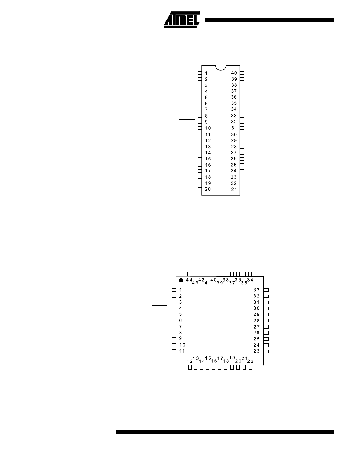
Pin Configurations Figure 1. Pinouts ATmega16
PDIP
(XCK/T0) PB0
(T1) PB1
(INT2/AIN0) PB2
(OC0/AIN1) PB3
(SS) PB4
(MOSI) PB5
(MISO) PB6
(SCK) PB7
RESET
VCC
GND
XTAL2
XTAL1
(RXD) PD0
(TXD) PD1
(INT0) PD2
(INT1) PD3
(OC1B) PD4
(OC1A) PD5
(ICP) PD6
PA0 (ADC0)
PA1 (ADC1)
PA2 (ADC2)
PA3 (ADC3)
PA4 (ADC4)
PA5 (ADC5)
PA6 (ADC6)
PA7 (ADC7)
AREF
GND
AVCC
PC7 (TOSC2)
PC6 (TOSC1)
PC5 (TDI)
PC4 (TDO)
PC3 (TMS)
PC2 (TCK)
PC1 (SDA)
PC0 (SCL)
PD7 (OC2)
TQFP
PB4 (SS)
PB3 (AIN1/OC0)
PB2 (AIN0/INT2)
PB1 (T1)
PB0 (XCK/T0)
GND
VCC
PA0 (ADC0)
PA1 (ADC1)
PA2 (ADC2)
PA3 (ADC3)
(MOSI) PB5
(MISO) PB6
(SCK) PB7
RESET
VCC
GND
XTAL2
XTAL1
(RXD) PD0
(TXD) PD1
(INT0) PD2
VCC
GND
(ICP) PD6
(INT1) PD3
(OC1B) PD4
2
ATmega16(L)
(OC2) PD7
(OC1A) PD5
(SCL) PC0
(TCK) PC2
(SDA) PC1
(TMS) PC3
PA4 (ADC4)
PA5 (ADC5)
PA6 (ADC6)
PA7 (ADC7)
AREF
GND
AVCC
PC7 (TOSC2)
PC6 (TOSC1)
PC5 (TDI)
PC4 (TDO)
2466BS–09/01
Page 3
ATmega16(L)
Overview The ATmega16 is a low-power CMOS 8-bit microcontroller based on the AVR enhanced
RISC architecture. By executing powerful instructions in a single clock cycle, the
ATmega16 achieves throughputs approaching 1 MIPS per MHz allowing the system
designer to optimize power consumption versus processing speed.
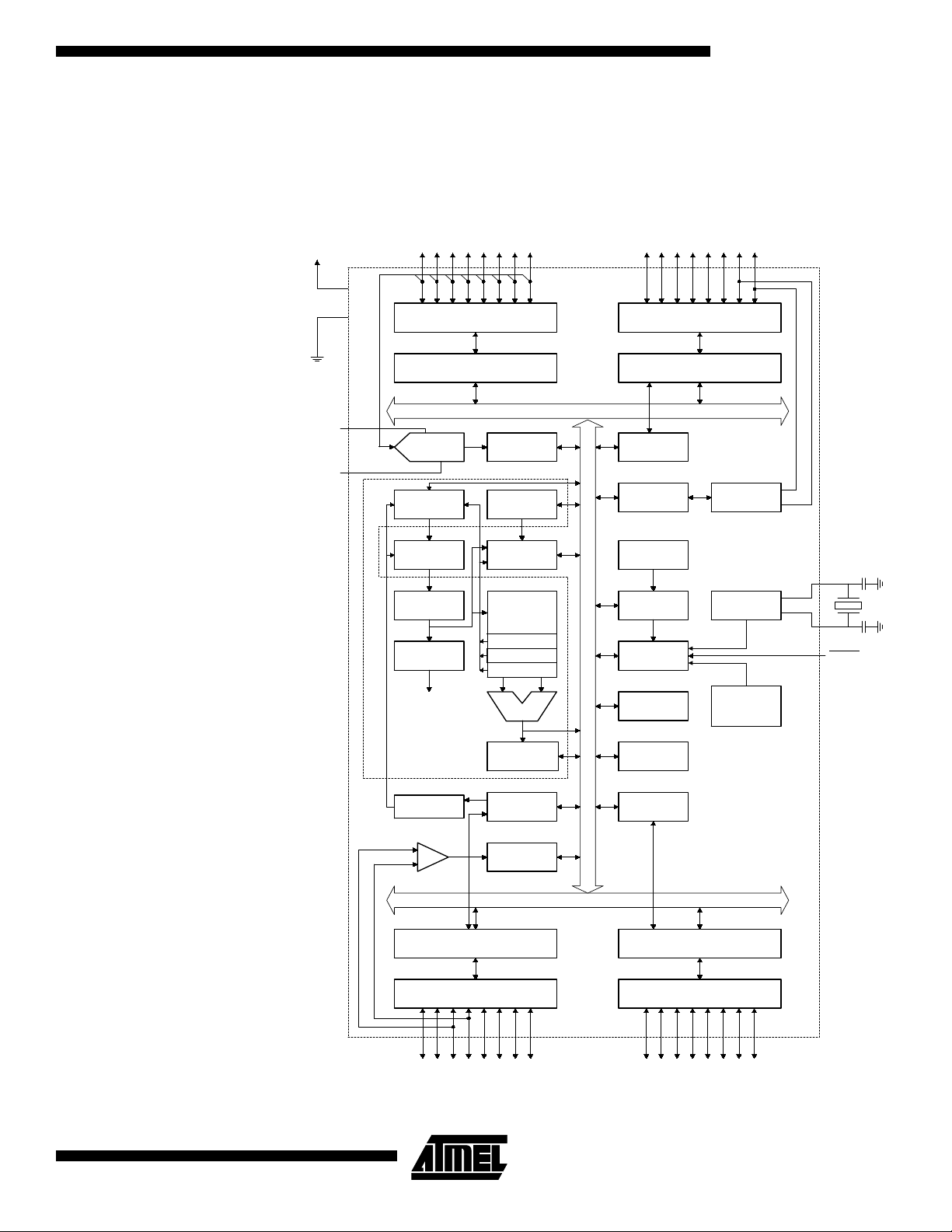
Block Diagram Figure 2. Block Diagram
VCC
PA0 - PA7 PC0 - PC7
GND
AVCC
AREF
PORTA DRIVERS/BUFFERS
PORTA DIGITAL INTERFACE
MUX &
ADC
PROGRAM
COUNTER
PROGRAM
FLASH
INSTRUCTION
REGISTER
INSTRUCTION
DECODER
CONTROL
LINES
AVR CPU
ADC
INTERFACE
STACK
POINTER
SRAM
GENERAL
PURPOSE
REGISTERS
X
Y
Z
ALU
STATUS
REGISTER
PORTC DRIVERS/BUFFERS
PORTC DIGITAL INTERFACE
TWI
TIMERS/
COUNTERS
INTERNAL
OSCILLATOR
WATCHDOG
TIMER
MCU CTRL.
& TIMING
INTERRUPT
UNIT
EEPROM
OSCILLATOR
OSCILLATOR
INTERNAL
CALIBRATED
OSCILLATOR
XTAL1
XTAL2
RESET
2466BS–09/01
PROGRAMMING
LOGIC
+
-
PORTB DIGITAL INTERFACE
PORTB DRIVERS/BUFFERS
SPI
COMP.
INTERFACE
USART
PORTD DIGITAL INTERFACE
PORTD DRIVERS/BUFFERS
PD0 - PD7PB0 - PB7
3
Page 4

The AVR core combines a rich instruction set with 32 general purpose working registers.
All the 32 registers are directly connected to the Arithmetic Logic Unit (ALU), allowing
two independent registers to be accessed in one single instruction executed in one clock
cycle. The resulting architecture is more code efficient while achieving throughputs up to
ten times faster than conventional CISC microcontrollers.
The ATmega16 provides the following features: 16K bytes of In-System Programmable
Flash with Read-While-Write capabilities, 512 bytes EEPROM, 1K byte SRAM, 32 general-purpose I/O lines, 32 general purpose working registers, a JTAG interface for
Boundary-scan, On-chip Debugging support and programming, three flexible
timer/counters with compare modes, internal and external interrupts, a serial programmable USART, a byte oriented 2-wire Serial Interface, an 8-channel, 10-bit ADC with
optional differential input stage with programmable gain (TQFP package only), a programmable Watchdog Timer with internal oscillator, an SPI serial port, and six software
selectable power saving modes. The Idle mode stops the CPU while allowing the
SRAM, timer/counters, SPI port, and interrupt system to continue functioning. The
Power-down mode saves the register contents but freezes the oscillator, disabling all
other chip functions until the next interrupt or hardware reset. In Power-save mode, the
asynchronous timer continues to run, allowing the user to maintain a timer base while
the rest of the device is sleeping. The ADC Noise Reduction Mode stops the CPU and
all I/O modules except asynchronous timer and ADC, to minimize switching noise during
ADC conversions. In Standby mode, the crystal/resonator oscillator is running while the
rest of the device is sleeping. This allows very fast start-up combined with low-power
consumption. In Extended Standby mode, both the main oscillator and the asynchronous timer continue to run.
The device is manufactured using Atmel’s high density nonvolatile memory technology.
The On-chip ISP Flash allows the program memory to be reprogrammed in-system
through an SPI serial interface, by a conventional nonvolatile memory programmer, or
by an On-chip Boot program running on the AVR core. The boot program can use any
interface to download the application program in the Application Flash memory. Software in the Boot Flash section will continue to run while the Application Flash section is
updated, providing true Read-While-Write operation. By combining an 8-bit RISC CPU
with In-System Self-Programmable Flash on a monolithic chip, the Atmel ATmega16 is
a powerful microcontroller that provides a highly-flexible and cost-effective solution to
many embedded control applications.
The ATmega16 AVR is supported with a full suite of program and system development
tools including: C compilers, macro assemblers, program debugger/simulators, in-circuit
emulators, and evaluation kits.
Pin Descriptions
VCC Digital supply voltage.
GND Ground.
Port A (PA7..PA0) Port A serves as the analog inputs to the A/D Converter.
Port A also serves as an 8-bit bi-directional I/O port, if the A/D Converter is not used.
Port pins can provide internal pull-up resistors (selected for each bit). The Port A output
buffers have symmetrical drive characteristics with both high sink and source capability.
When pins PA0 to PA7 are used as inputs and are externally pulled low, they will source
current if the internal pull-up resistors are activated. The Port A pins are tristated when a
reset condition becomes active, even if the clock is not running.
4
ATmega16(L)
2466BS–09/01
Page 5

ATmega16(L)
Port B (PB7..PB0) Port B is an 8-bit bi-directional I/O port with internal pull-up resistors (selected for each
bit). The Port B output buffers have symmetrical drive characteristics with both high sink
and source capability. As inputs, Port B pins that are externally pulled low will source
current if the pull-up resistors are activated. The Port B pins are tristated when a reset
condition becomes active, even if the clock is not running.
Port B also serves the functions of various special features of the ATmega16 as listed
on page 55.
Port C (PC7..PC0) Port C is an 8-bit bi-directional I/O port with internal pull-up resistors (selected for each
bit). The Port C output buffers have symmetrical drive characteristics with both high sink
and source capability. As inputs, Port C pins that are externally pulled low will source
current if the pull-up resistors are activated. The Port C pins are tristated when a reset
condition becomes active, even if the clock is not running. If the JTAG interface is
enabled, the pull-up resistors on pins PC5(TDI), PC3(TMS) and PC2(TCK) will be activated even if a reset occurs.
Port C also serves the functions of the JTAG interface and other special features of the
ATmega16 as listed on page 58.
Port D (PD7..PD0) Port D is an 8-bit bidirectional I/O port with internal pull-up resistors (selected for each
bit). The Port D output buffers have symmetrical drive characteristics with both high sink
and source capability. As inputs, Port D pins that are externally pulled low will source
current if the pull-up resistors are activated. The Port D pins are tristated when a reset
condition becomes active, even if the clock is not running.
Port D also serves the functions of various special features of the ATmega16 as listed
on page 60.
RESET
XTAL1 Input to the inverting oscillator amplifier and input to the internal clock operating circuit.
XTAL2 Output from the inverting oscillator amplifier.
AVCC This is the supply voltage pin for Port A and the A/D Converter. It should be externally
AREF This is the analog reference pin for the A/D Converter.
Reset input. A low level on this pin for longer than the minimum pulse length will generate a reset, even if the clock is not running. The minimum pulse length is given in Table
15 on page 35. Shorter pulses are not guaranteed to generate a reset.
connected to VCC, even if the ADC is not used. If the ADC is used, it should be connected to VCC through a low-pass filter.
2466BS–09/01
5
Page 6

Register Summary
Address Name Bit 7 Bit 6 Bit 5 Bit 4 Bit 3 Bit 2 Bit 1 Bit 0 Page
$3F ($5F) SREG I T H S V N Z C 7
$3E ($5E) SPH - - - - - SP10 SP9 SP8 10
$3D ($5D) SPL SP7 S P6 SP5 SP4 SP3 S P2 SP1 SP0 10
$3C ($5C) OCR0
$3B ($5B) GICR INT1 INT0 INT2 - - - IVSEL IVCE 45, 65
$3A ($5A) GIFR INTF1 INTF0 INTF2 - - - - -66
$39 ($59) TIMSK OCIE2 TOIE2 TICIE1 OCIE1A OCIE1B TOIE1 OCIE0 TOIE0 80, 109, 126
$38 ($58) TIFR OCF2 TOV2 ICF1 OCF1A OCF1B TOV1 OCF0 TOV0 80, 109, 126
$37 ($57) SPMCR SPMIE RWWSB - RWWSRE BLBSET PGWRT PGERS SPMEN 245
$36 ($56) TWCR TWINT TWEA TWSTA TWSTO TWWC TWEN
$35 ($55) MCUCR SM2 SE SM1 SM0 ISC11 ISC10 ISC01 ISC00 30, 64
$34 ($54) MCUCSR JTD ISC2
$33 ($53) TCCR0 FOC0 WGM00 COM01 COM00 WGM01 CS02 CS01 CS00 77
$32 ($52) TCNT0 Timer/Counter0 (8 Bits) 79
(1)
$31
($51)
$30 ($50) SFIOR ADTS2 ADTS1 ADTS0 ADHSM ACME PUD PSR2 PSR10 53,82,127,192,213
$2F ($4F) TCCR1A COM1A1 COM1A0 COM1B1 COM1B0 FOC1A FOC1B WGM11 WGM10 104
$2E ($4E) TCCR1B ICNC1 ICES1 - WGM13 WGM12 CS12 CS11 CS10 107
$2D ($4D) TCNT1H Timer/Counter1 - Counter Register High Byte 108
$2C ($4C) TCNT1L Timer/Counter1 - Counter Register Low Byte 108
$2B ($4B) OCR1AH
$2A ($4A) OCR1AL
$29 ($49) OCR1BH
$28 ($48) OCR1BL
$27 ($47) ICR1H Timer/Counter1 - Input Capture Register High Byte 108
$26 ($46) ICR1L Timer/Counter1 - Input Capture Register Low Byte 108
$25 ($45) TCCR2 FOC2 WGM20 COM21 COM20 WGM21 CS22 CS21 CS20 121
$24 ($44) TCNT2 Timer/Counter2 (8 Bits) 123
$23 ($43) OCR2
$22 ($42) ASSR - - - - AS2 TCN2UB OCR2UB TCR2UB 124
$21 ($41) WDTCR - - - WDTOE WDE WDP2 WDP1 WDP0 40
(2)
$20
($40)
$1F ($3F) EEARH - - - - - - - EEAR8 16
$1E ($3E) EEARL EEPROM Address Register Low Byte 16
$1D ($3D) EEDR EEPROM Data Register 16
$1C ($3C) EECR - - - - EERIE EEMWE EEWE EERE 17
$1B ($3B) PORTA PORTA7 PORTA6 PORTA5 PORTA4 PORTA3 PORTA2 PORTA1 PORTA0 62
$1A ($3A) DDRA DDA7 DDA6 DDA5 DDA4 DDA3 DDA2 DDA1 DDA0 62
$19 ($39) PINA PINA7 PINA6 PINA5 PINA4 PINA3 PINA2 PINA1 PINA0 62
$18 ($38) PORTB PORTB7 PORTB6 PORTB5 PORTB4 PORTB3 PORTB2 PORTB1 PORTB0 62
$17 ($37) DDRB DDB7 DDB6 DDB5 DDB4 DDB3 DDB2 DDB1 DDB0 62
$16 ($36) PINB PINB7 PINB6 PINB5 PINB4 PINB3 PINB2 PINB1 PINB0 62
$15 ($35) PORTC PORTC7 PORTC6 PORTC5 PORTC4 PORTC3 PORTC2 PORTC1 PORTC0 62
$14 ($34) DDRC DDC7 DDC6 DDC5 DDC4 DDC3 DDC2 DDC1 DDC0 62
$13 ($33) PINC PINC7 PINC6 PINC5 PINC4 PINC3 PINC2 PINC1 PINC0 63
$12 ($32) PORTD PORTD7 PORTD6 PORTD5 PORTD4 PORTD3 PORTD2 PORTD1 PORTD0 63
$11 ($31) DDRD DDD7 DDD6 DDD5 DDD4 DDD3 DDD2 DDD1 DDD0 63
$10 ($30) PIND PIND7 PIND6 PIND5 PIND4 PIND3 PIND2 PIND1 PIND0 63
$0F ($2F) SPDR SPI Data Register 134
$0E ($2E) SPSR SPIF WCOL - - - - -SPI2X 133
$0D ($2D) SPCR SPIE SPE DORD MSTR CPOL CPHA SPR1 SPR0 132
$0C ($2C) UDR USART I/O Data Register 155
$0B ($2B) UCSRA RXC TXC UDRE FE DOR PE U2X MPCM 156
$0A ($2A) UCSRB RXCIE TXCIE UDRIE RXEN TXEN UCSZ2 RXB8 TXB8 157
$09 ($29) UBRRL USART Baud Rate Register Low Byte 159
$08 ($28) ACSR ACD ACBG ACO ACI ACIE ACIC ACIS1 ACIS0 192
$07 ($27) ADMUX REFS1 REFS0 ADLAR MUX4 MUX3 MUX2 MUX1 MUX0 209
$06 ($26) ADCSRA ADEN ADSC ADFR ADIF ADIE ADPS2 ADPS1 ADPS0 211
$05 ($25) ADCH ADC Data Register High Byte 212
$04 ($24) ADCL ADC Data Register Low Byte 212
$03 ($23) TWDR 2-wire Serial Interface Data Register 172
OSCCAL Oscillator Calibration Register 28
(1)
OCDR On-Chip Debug Register 219
UBRRH URSEL - - - UBRR[11:8] 159
(2)
UCSRC URSEL UMSEL UPM1 UPM0 USBS UCSZ1 UCSZ0 UCPOL 158
Timer/Counter0 Output Compare Register
- JTRF WDRF BORF EXTRF PORF 38, 65, 223
Timer/Counter1 - Output Compare Register A High Byte
Timer/Counter1 - Output Compare Register A Low Byte
Timer/Counter1 - Output Compare Register B High Byte
Timer/Counter1 - Output Compare Register B Low Byte
Timer/Counter2 Output Compare Register
80
-TWIE 171
108
108
108
108
123
6
ATmega16(L)
2466BS–09/01
Page 7

ATmega16(L)
Register Summary (Continued)
Address Name Bit 7 Bit 6 Bit 5 Bit 4 Bit 3 Bit 2 Bit 1 Bit 0 Page
$02 ($22) TWAR TWA6 TWA5 TWA4 TWA3 TWA2 TWA1 TWA0 TWGCE 173
$01 ($21) TWSR TWS7
$00 ($20) TWBR 2-wire Serial Interface Bit Rate Register 171
Notes: 1. When the OCDEN fuse is unprogrammed, the OSCCAL register is always accessed on this address. Refer to the debugger
specific documentation for details on how to use the OCDR register.
2. Refer to the USART description for details on how to access UBRRH and UCSRC.
3. For compatibility with future devices, reserved bits should be written to zero if accessed. Reserved I/O memory addresses
should never be written.
4. Some of the status flags are cleared by writing a logical one to them. Note that the CBI and SBI instructions will operate on
all bits in the I/O register, writing a one back into any flag read as set, thus clearing the flag. The CBI and SBI instructions
work with registers $00 to $1F only.
TWS6 TWS5 TWS4 TWS3
-
TWPS1 TWPS0
172
2466BS–09/01
7
Page 8

Instruction Set Summary
Mnemonics Operands Description Operation Flags #Clocks
ARITHMETIC AND LOGIC INSTRUCTIONS
ADD Rd, Rr Add two Registers Rd ← Rd + Rr Z,C,N,V,H 1
ADC Rd, Rr Add with Carry two Registers Rd ← Rd + Rr + C Z,C,N,V,H 1
ADIW Rdl,K Add Immediate to Word Rdh:Rdl ← Rdh:Rdl + K Z,C,N,V ,S 2
SUB Rd, Rr Subtract two Registers Rd ← Rd - Rr Z,C,N,V,H 1
SUBI Rd, K Subtract Constant from Register Rd ← Rd - K Z,C,N,V,H 1
SBC Rd, Rr Subtract with Carry two Registers Rd ← Rd - Rr - C Z,C,N,V,H 1
SBCI Rd, K Subtract with Carry Constant from Reg. Rd ← Rd - K - C Z,C,N,V,H 1
SBIW Rdl,K Subtract Immediate from Word Rdh:Rdl ← Rdh:Rdl - K Z,C,N,V ,S 2
AND Rd, Rr Logical AND Registers Rd ←=Rd • Rr Z,N,V 1
ANDI Rd, K Logical AND Register and Constant Rd ← Rd •=KZ,N,V1
OR Rd, Rr Logical OR Registers Rd ← Rd v Rr Z,N,V 1
ORI Rd, K Logical OR Register and Constant Rd ←=Rd v K Z,N,V 1
EOR Rd, Rr Exclusive OR Registers Rd ← Rd ⊕ Rr Z,N,V 1
COM Rd One"s Complement Rd ← $FF − Rd Z,C,N,V 1
NEG Rd Two"s Complement Rd ← $00 − Rd Z,C,N,V,H 1
SBR Rd,K Set Bit(s) in Register Rd ← Rd v K Z,N,V 1
CBR Rd,K Clear Bit(s) in Register Rd ← Rd • ($FF - K) Z,N,V 1
INC Rd Increment Rd ← Rd + 1 Z,N,V 1
DEC Rd Decrement Rd ← Rd − 1 Z,N,V 1
TST Rd Test for Zero or Minus Rd ← Rd • Rd Z,N,V 1
CLR Rd Clear Register Rd ← Rd ⊕ Rd Z,N,V 1
SER Rd Set Register Rd ← $FF None 1
MUL Rd, Rr Multiply Unsigned R1:R0 ← Rd x Rr Z,C 2
MULS Rd, Rr Multiply Signed R1:R0 ← Rd x Rr Z,C 2
MULSU Rd, Rr Multiply Signed with Unsigned R1:R0 ← Rd x Rr Z,C 2
FMUL Rd, Rr Fractional Multiply Unsigned R1:R0 ← (Rd x Rr ) << 1 Z,C 2
FMULS Rd, Rr Fractional Multiply Signed R1:R0 ← (Rd x Rr) << 1 Z,C 2
FMULSU Rd, Rr Fractional Multiply Signed with Unsigned R1:R0 ← (Rd x Rr) << 1 Z,C 2
BRANCH INSTRUCTIONS
RJMP k Relative Jump PC=← PC + k + 1 None 2
IJMP Indirect Jump to (Z) PC ← Z None 2
JMP k Direct Jump PC=← kNone3
RCALL k Relative Subroutine Call PC ← PC + k + 1 None 3
ICALL Indirect Call to (Z) PC ← ZNone3
CALL k Direct Subroutine Call PC ← kNone4
RET Subroutine Return PC ← STACK None 4
RETI Interrupt Return PC ← STACK I 4
CPSE Rd,Rr Compare, Skip if Equal if (Rd = Rr) PC=← PC + 2 or 3 None 1 / 2 / 3
CP Rd,Rr Compare Rd − Rr Z, N,V,C,H 1
CPC Rd,Rr Compare with Carry Rd − Rr − C Z, N,V,C,H 1
CPI Rd,K Compare Register with Immediate Rd − K Z, N,V,C,H 1
SBRC Rr, b Skip if Bit in Register Cleared if (Rr(b)=0) PC ← PC + 2 or 3 None 1 / 2 / 3
SBRS Rr, b Skip if Bit in Register is Set if (Rr(b)=1) PC ← PC + 2 or 3 None 1 / 2 / 3
SBIC P, b Skip if Bit in I/O Register Cleared if (P(b)=0) PC ← PC + 2 or 3 None 1 / 2 / 3
SBIS P, b Skip if Bit in I/O Register is Set if (P(b)=1) PC ← PC + 2 or 3 None 1 / 2 / 3
BRBS s, k Branch if Status Flag Set if (SREG(s) = 1) then PC←PC+k + 1 None 1 / 2
BRBC s, k Branch if Status Flag Cleared if (SREG(s) = 0) then PC←PC+k + 1 None 1 / 2
BREQ k Branch if Equal if (Z = 1) then PC ← PC + k + 1 None 1 / 2
BRNE k Branch if Not Equal if (Z = 0) then PC ← PC + k + 1 None 1 / 2
BRCS k Branch if Carry Set if (C = 1) then PC ← PC + k + 1 None 1 / 2
BRCC k Branch if Carry Cleared if (C = 0) then PC ← PC + k + 1 None 1 / 2
BRSH k Branch if Same or Higher if (C = 0) then PC ← PC + k + 1 None 1 / 2
BRLO k Branch if Lower if (C = 1) then PC ← PC + k + 1 None 1 / 2
BRMI k Branch if Minus if (N = 1) then PC ← PC + k + 1 None 1 / 2
BRPL k Branch if Plus if (N = 0) then PC ← PC + k + 1 None 1 / 2
BRGE k Branch if Greater or Equal, Signed if (N ⊕ V= 0) then PC ← PC + k + 1 None 1 / 2
BRLT k Branch if Less Than Zero, Signed if (N ⊕ V= 1) then PC ← PC + k + 1 None 1 / 2
BRHS k Branch if Half Carry Flag Set if (H = 1) then PC ← PC + k + 1 None 1 / 2
BRHC k Branch if Half Carry Flag Cleared if (H = 0) then PC ← PC + k + 1 None 1 / 2
BRTS k Branch if T Flag Set if (T = 1) then PC ← PC + k + 1 None 1 / 2
BRTC k Branch if T Flag Cleared if (T = 0) then PC ← PC + k + 1 None 1 / 2
BRVS k Branch if Overflow Flag is Set if (V = 1) then PC ← PC + k + 1 None 1 / 2
BRVC k Branch if Overflow Flag is Cleared if (V = 0) then PC ← PC + k + 1 None 1 / 2
8
ATmega16(L)
2466BS–09/01
Page 9

ATmega16(L)
Instruction Set Summary (Continued)
BRIE k Branch if Interrupt Enabled if ( I = 1) then PC ← PC + k + 1 None 1 / 2
BRID k Branch if Interrupt Disabled if ( I = 0) then PC ← PC + k + 1 None 1 / 2
DATA TRANSFER INSTRUCTIONS
MOV Rd, Rr Move Between Registers Rd ← Rr None 1
MOVW Rd, Rr Copy Register Word
LDI Rd, K Load Immediate Rd ← KNone1
LD Rd, X Load Indirect Rd ← (X) None 2
LD Rd, X+ Load Indirect and Post-Inc. Rd ← (X), X ← X + 1 None 2
LD Rd, - X Load Indirect and Pre-Dec. X ← X - 1, Rd ← (X) None 2
LD Rd, Y Load Indirect Rd ← (Y) None 2
LD Rd, Y+ Load Indirect and Post-Inc. Rd ← (Y), Y ← Y + 1 None 2
LD Rd, - Y Load Indirect and Pre-Dec. Y ← Y - 1, Rd ← (Y) None 2
LDD Rd,Y+q Load Indirect with Displacement Rd ← (Y + q) None 2
LD Rd, Z Load Indirect Rd ← (Z) None 2
LD Rd, Z+ Load Indirect and Post-Inc. Rd ← (Z), Z ← Z+1 None 2
LD Rd, -Z Load Indirect and Pre-Dec. Z ← Z - 1, Rd ← (Z) None 2
LDD Rd, Z+q Load Indirect with Displacement Rd ← (Z + q) None 2
LDS Rd, k Load Direct from SRAM Rd ← (k) None 2
ST X, Rr Store Indirect (X)=← Rr None 2
ST X+, Rr Store Indirect and Post-Inc. (X)=← Rr, X ← X + 1 None 2
ST - X, Rr Store Indirect and Pre-Dec. X ← X - 1, (X) ← Rr None 2
ST Y, Rr Store Indirect (Y) ← Rr None 2
ST Y+, Rr Store Indirect and Post-Inc. (Y) ← Rr, Y ← Y + 1 None 2
ST - Y, Rr Store Indirect and Pre-Dec. Y ← Y - 1, (Y) ← Rr None 2
STD Y+q,Rr Store Indirect with Displacement (Y + q) ← Rr None 2
ST Z, Rr Store Indirect (Z) ← Rr None 2
ST Z+, Rr Store Indirect and Post-Inc. (Z) ← Rr, Z ← Z + 1 None 2
ST -Z, Rr Store Indirect and Pre-Dec. Z ← Z - 1, (Z) ← Rr None 2
STD Z+q,Rr Store Indirect with Displacement (Z + q) ← Rr None 2
STS k, Rr Store Direct to SRAM (k) ← Rr None 2
LPM Load Program Memory R0 ← (Z) None 3
LPM Rd, Z Load Program Memory Rd ← (Z) None 3
LPM Rd, Z+ Load Program Memory and Post-Inc Rd ← (Z), Z ← Z+1 None 3
SPM Store Program Memory (Z) ← R1:R0 None -
IN Rd, P In Port Rd ← PNone1
OUT P, Rr Out Port P ← Rr None 1
PUSH Rr Push Register on Stack STACK ← Rr None 2
POP Rd Pop Register from Stack Rd ← STACK None 2
BIT AND BIT-TEST INSTRUCTIONS
SBI P,b Set Bit in I/O Register I/O(P,b) ← 1None2
CBI P,b Clear Bit in I/O Register I/O(P,b) ← 0None2
LSL Rd Logical Shift Left Rd(n+1) ← Rd(n), Rd(0) ← 0 Z,C,N,V 1
LSR Rd Logical Shift Right Rd(n) ← Rd(n+1), Rd(7) ← 0 Z,C,N ,V 1
ROL Rd Rotate Left Through Carry Rd(0)←C,Rd(n+1)← Rd(n),C←R d(7) Z,C,N,V 1
ROR Rd Rotate Right Through Carry Rd(7)←C,Rd(n)← Rd(n+1),C←Rd(0) Z,C,N ,V 1
ASR Rd Arithmetic Shift Right Rd(n) ← Rd(n+1), n=0..6 Z,C,N,V 1
SWAP Rd Swap Nibbles Rd(3..0)←Rd(7..4),Rd(7..4)←Rd(3..0) None 1
BSET s Flag Set SREG(s) ← 1 SREG(s) 1
BCLR s Flag Clear SREG(s) ← 0 SREG(s) 1
BST Rr, b Bit Store from Register to T T ← Rr(b) T 1
BLD Rd, b Bit load from T to Register Rd(b) ← TNone1
SEC Set Carry C ← 1C1
CLC Clear Carry C ← 0 C 1
SEN Set Negative Flag N ← 1N1
CLN Clear Negative Flag N ← 0 N 1
SEZ Set Zero Flag Z ← 1Z1
CLZ Clear Zero Flag Z ← 0 Z 1
SEI Global Interrupt Enable I ← 1I1
CLI Global Interrupt Disable I=← 0 I 1
SES Set Signed Test Flag S ← 1S1
CLS Clear Signed Test Flag S ← 0 S 1
SEV Set Twos Complement Overflow. V ← 1V1
CLV Clear Twos Complement Overflow V ← 0 V 1
SET Set T in SREG T ← 1T1
CLT Clear T in SREG T ← 0 T 1
SEH Set Half Carry Flag in SREG H ← 1H1
Rd+1:Rd ← Rr+1:Rr
None 1
2466BS–09/01
9
Page 10

Instruction Set Summary (Continued)
CLH Clear Half Carry Flag in SREG H ← 0 H 1
MCU CONTROL INSTRUCTIONS
NOP No Operation None 1
SLEEP Sleep (see specific descr. for Sleep function) None 1
WDR Watchdog Reset (see specific descr. for WDR/timer) None 1
BREAK Break For On-Chip Debug Only None N/A
10
ATmega16(L)
2466BS–09/01
Page 11

ATmega16(L)
Ordering Information
Speed (MHz) Power Supply Ordering Code Package Operation Range
8 2.7 - 5.5V ATmega16L-8AC
ATmega16L-8PC
ATmega16L-8AI
ATmega16L-8PI
16 4.5 - 5.5V ATmega16-16AC
ATmega16-16PC
ATmega16-16AI
ATmega16-16PI
44A
40P6
44A
40P6
44A
40P6
44A
40P6
Commercial
o
C to 70oC)
(0
Industrial
(-40oC to 85oC)
Commercial
o
C to 70oC)
(0
Industrial
o
(-40
C to 85oC)
Package Type
44A 44-lead, Thin (1.0 mm) Plastic Gull Wing Quad Flat Package (TQFP)
40P6 40-pin, 0.600” Wide, Plastic Dual Inline Package (PDIP)
2466BS–09/01
11
Page 12

Packaging Information
44A
44-lead, Thin (1.0mm) Plastic Quad Flat Package
(TQFP), 10x10mm body, 2.0mm footprint, 0.8mm pitch.
Dimension in Millimeters and (Inches)*
JEDEC STANDARD MS-026 ACB
PIN 1 ID
0.80(0.0315) BSC
0.20(0.008)
0.09(0.004)
0˚~7˚
PIN 1
0.75(0.030)
0.45(0.018)
12.25(0.482)
11.75(0.462)
10.10(0.394)
9.90(0.386)
0.15(0.006)
0.05(0.002)
SQ
0.45(0.018)
0.30(0.012)
SQ
1.20(0.047) MAX
12
*Controlling dimension: millimetter
REV. A 04/11/2001
ATmega16(L)
2466BS–09/01
Page 13

40P6
52.71(2.075)
51.94(2.045)
PIN
1
13.97(0.550)
13.46(0.530)
0.38(0.015)MIN
0.56(0.022)
0.38(0.015)
REF
15.88(0.625)
15.24(0.600)
1.65(0.065)
1.27(0.050)
17.78(0.700)MAX
0.38(0.015)
0.20(0.008)
2.54(0.100)BSC
3.56(0.140)
3.05(0.120)
SEATING
PLANE
4.83(0.190)MAX
48.26(1.900) REF
ATmega16(L)
40-lead, Plastic Dual Inline
Parkage (PDIP), 0.600" wide
Demension in Millimeters and (Inches)*
JEDEC STANDARD MS-011 AC
*Controlling dimension: Inches
0º ~ 15º
REV. A 04/11/2001
2466BS–09/01
13
Page 14

Atmel Headquarters Atmel Product Operations
Corporate Headquarters
2325 Orchard Parkway
San Jose, CA 95131
TEL (408) 441-0311
FAX (408) 487-2600
Europe
Atmel SarL
Route des Arsenaux 41
Casa Postale 80
CH-1705 Fribourg
Switzerland
TEL (41) 26-426-5555
FAX (41) 26-426-5500
Asia
Atmel Asia, Ltd.
Room 1219
Chinachem Golden Plaza
77 Mody Road Tsimhatsui
East Kowloon
Hong Kong
TEL (852) 2721-9778
FAX (852) 2722-1369
Japan
Atmel Japan K.K.
9F, Tonetsu Shinkawa Bldg.
1-24-8 Shinkawa
Chuo-ku, Tokyo 104-0033
Japan
TEL (81) 3-3523-3551
FAX (81) 3-3523-7581
Atmel Colorado Springs
1150 E. Cheyenne Mtn. Blvd.
Colorado Springs, CO 80906
TEL (719) 576-3300
FAX (719) 540-1759
Atmel Grenoble
Avenue de Rochepleine
BP 123
38521 Saint-Egreve Cedex, France
TEL (33) 4-7658-3000
FAX (33) 4-7658-3480
Atmel Heilbronn
Theresienstrasse 2
POB 3535
D-74025 Heilbronn, Germany
TEL (49) 71 31 67 25 94
FAX (49) 71 31 67 24 23
Atmel Nantes
La Chantrerie
BP 70602
44306 Nantes Cedex 3, France
TEL (33) 0 2 40 18 18 18
FAX (33) 0 2 40 18 19 60
Atmel Rousset
Zone Industrielle
13106 Rousset Cedex, France
TEL (33) 4-4253-6000
FAX (33) 4-4253-6001
Atmel Smart Card ICs
Scottish Enterprise Technology Park
East Kilbride, Scotland G75 0QR
TEL (44) 1355-357-000
FAX (44) 1355-242-743
e-mail
literature@atmel.com
Web Site
http://www.atmel.com
BBS
1-(408) 436-4309
© Atmel Corporation 2001.
Atmel Corporation makes no warranty for the use of its products, other than those expressly contained in the Company’s standard warranty
which is detailed in Atmel’s Terms and Conditions located on the Company’s web site. The Company assumes no responsibility for any errors
which may appear in this document, reserves the right to change devices or specifications detailed herein at any time without notice, and does
not make any commitment to update the information contained herein. No licenses to patents or other intellectual property of Atmel are granted
by the Company in connection with the sale of Atmel products, expressly or by implication. Atmel’s products are not authorized for use as critical
components in life support devices or systems.
AT ME L®, AVR® and AVR Studio® are the registered trademarks of Atmel.
Microsoft
Other terms and product names may be the trademarks of others.
®
, Windows® and Windows NT® are the registered trademarks of Microsoft Corporation.
Printed on recycled paper.
2466BS–09/01/xM
 Loading...