

Page 1

ATmega128RFA1
Features
• High Performance, Low Power AVR® 8-Bit Microcontroller
• Advanced RISC Architecture
- 135 Powerful Instructions – Most Single Clock Cycle Execution
- 32x8 General Purpose Working Registers
- Fully Static Operation
- Up to 16 MIPS Throughput at 16 MHz and 1.8V
- On-Chip 2-cycle Multiplier
• Non-volatile Program and Data Memories
- 128K Bytes of In-System Self-Programmable Flash
• Endurance: 2000 Write/Erase Cycles @ 85°C
- 4K Bytes EEPROM
• Endurance: 2000 Write/Erase Cycles @ 85°C
- 16K Bytes Internal SRAM
• JTAG (IEEE std. 1149.1 compliant) Interface
- Boundary-scan Capabilities According to the JTAG Standard
- Extensive On-chip Debug Support
- Programming of Flash EEPROM, Fuses and Lock Bits through the JTAG interface
• Peripheral Features
- Multiple Timer/Counter & PWM channels
- Real Time Counter with Separate Oscillator
- 10-bit, 330 ks/s A/D Converter; Analog Comparator; On-chip Temperature Sensor
- Master/Slave SPI Serial Interface
- Two Programmable Serial USART
- Byte Oriented 2-wire Serial Interface
• Advanced Interrupt Handler
• Watchdog Timer with Separate On-Chip Oscillator
• Power-on Reset and Low Current Brown-Out Detector
• Advanced Power Save Modes
• Fully integrated Low Power Transceiver for 2.4 GHz ISM Band
- Supported Data Rates: 250 kb/s and 500 kb/s, 1 Mb/s, 2 Mb/s
- -100 dBm RX Sensitivity; TX Output Power up to 3.5 dBm
- Hardware Assisted MAC (Auto-Acknowledge, Auto-Retry)
- 32 Bit IEEE 802.15.4 Symbol Counter
- Baseband Signal Processing
- SFR-Detection, Spreading; De-Spreading; Framing ; CRC-16 Computation
- Antenna Diversity and TX/RX control
- TX/RX 128 Byte Frame Buffer
• Hardware Security (AES, True Random Generator)
• Integrated Crystal Oscillators (32.768 kHz & 16 MHz)
• I/O and Package
- 38 Programmable I/O Lines
- 64-pad QFN (RoHS/Fully Green)
• Temperature Range: -40°C to 85°C Industrial
• Supply voltage range 1.8V to 3.6V with integrated voltage regulators
• Ultra Low Power consumption (1.8 to 3.6V) for Rx/Tx & AVR: <18.6 mA
- CPU Active Mode (16MHz): 4.1 mA
- 2.4GHz Transceiver: RX_ON 12.5 mA / TX 14.5 mA (maximum TX output power)
- Deep Sleep Mode: <250nA @ 25°C
• Speed Grade: 0 – 16 MHz @ 1.8 – 3.6V
8-bit
Microcontroller
with Low Power
2.4GHz
Transceiver for
ZigBee and
IEEE 802.15.4
ATmega128RFA1
PRELIMINARY
Applications
• ZigBee® / IEEE 802.15.4-2006/2003™ – Full And Reduced Function Device (FFD/RFD)
• General Purpose 2.4GHz ISM Band Transceiver with Microcontroller
• RF4CE, SP100, WirelessHART™, ISM Applications and IPv6 / 6LoWPAN
8266A-MCU Wireless-12/09
8266A-MCU Wireless-12/09
1
Page 2
ATmega128RFA1
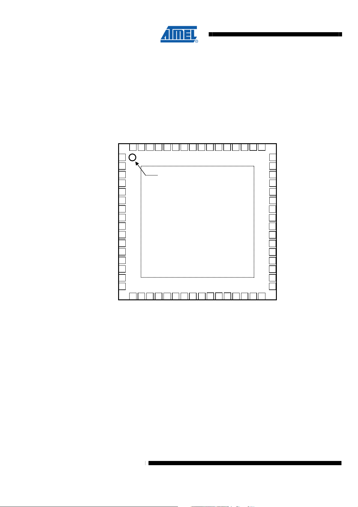
1 Pin Configurations
The large center pad underneath the QFN/MLF package is made of metal and internally connected
to AVSS. It should be soldered or glued to the board to ensure good mechanical stability. If the
62 61 60 59 58 57 64 63
17 18 19 20 21 23 22 24 25 26
[PD3:TXD1:INT3]
[PD2:RXD1:INT2]
[PD1:SDA:INT1]
[PD0:SCL:INT0]
[DVSS]
[DEVDD]
[DVDD]
[DVDD]
[DVSS:DSVSS]
[PG5:OC0B]
[PG4:TOSC1]
[PG3:TOSC2]
[PD7:T0]
[PD6:T1]
[PD5:XCK1]
[PD4:ICP1]
[PF2:ADC2:DIG2]
[PF3:ADC3:DIG4]
[PF4:ADC4:TCK]
[PF5:ADC5:TMS]
[PF6:ADC6:TDO]
[PF7:ADC7:TDI]
[AVSS_RFP]
[AVSS_RFN]
[PG0:DIG3]
[PG1:DIG1]
[PG2:AMR]
Figure 1-1. Pinout ATmega128RFA1
[PF1:ADC1]
[PF0:ADC0]
[AREF]
[AVSS:ASVSS]
[EVDD]
[AVDD]
[RFP]
[RFN]
[TST]
[RSTN]
[RSTON]
10
11
12
13
14
15
16
1
2
3
4
5
6
7
8
9
Index corner
Exposed paddle: [AVSS]
ATmega128RFA1
[XTAL2]
[AVSS]
[DVSS]
[XTAL1]
56 55 54 53 52 51
27
[DEVDD]
[PE7:ICP3:INT7:CLKO]
[PE6:T3:INT6]
[PE5:OC3C:INT5]
[PE4:OC3B:INT4]
[PE3:OC3A:AIN1]
50 49
[PE2:XCK0:AIN0]
48
[PE1:TXD0]
47
[PE0:RXD0:PCINT8]
46
[DVSS]
45
[DEVDD]
44
[PB7:OC0A:OC1C:PCINT7]
43
[PB6:OC1B:PCINT6]
42
[PB5:OC1A:PCINT5]
41
[PB4:OC2A:PCINT4]
40
[PB3:MISO:PDO:PCINT3]
39
[PB2:MOSI:PDI:PCINT2]
38
[PB1:SCK:PCINT1]
37
[PB0:SSN:PCINT0]
36
[DVSS]
35
[DEVDD]
34
[CLKI]
33
28
29
30
31 32
2 Disclaimer
2
Note:
center pad is left unconnected, the package might loosen from the board
Typical values contained in this datasheet are based on simulation and characterization
results of other AVR microcontrollers and radio transceivers manufactured in a similar
process technology. Minimum and Maximum values will be available after the device is
characterized.
8266A-MCU Wireless-12/09
Page 3
ATmega128RFA1
3 Overview
The ATmega128RFA1 is a low-power CMOS 8 bit microcontroller based on the AVR
enhanced RISC architecture combined with a high data rate transceiver for the 2.4 GHz
ISM band. It is derived from the ATmega1281 microcontroller and the AT86RF231 radio
transceiver.
By executing powerful instructions in a single clock cycle, the device achieves
throughputs approaching 1 MIPS per MHz allowing the system designer to optimize
power consumption versus processing speed.
The radio transceiver provides high data rates from 250 kb/s up to 2 Mb/s, frame
handling, outstanding receiver sensitivity and high transmit output power enabling a
very robust wireless communication.
3.1 Block Diagram
Figure 3-1 Block Diagram
8266A-MCU Wireless-12/09
The AVR core combines a rich instruction set with 32 general purpose working
registers. All 32 registers are directly connected to the Arithmetic Logic Unit (ALU). Two
independent registers can be accessed with one single instruction executed in one
clock cycle. The resulting architecture is very code efficient while achieving throughputs
up to ten times faster than conventional CISC microcontrollers. The system includes
internal voltage regulation and an advanced power management. Distinguished by the
small leakage current it allows an extended operation time from battery.
The radio transceiver is a fully integrated ZigBee solution using a minimum number of
external components. It combines excellent RF performance with low cost, small size
and low current consumption. The radio transceiver includes a crystal stabilized
fractional-N synthesizer, transmitter and receiver, and full Direct Sequence Spread
3
Page 4
ATmega128RFA1
Spectrum Signal (DSSS) processing with spreading and despreading. The device is
fully compatible with IEEE802.15.4-2006/2003 and ZigBee standards.
The ATmega128RFA1 provides the following features: 128 kbytes of In-System
Programmable (ISP) Flash with read-while-write capabilities, 4 kbytes EEPROM, 16
kbytes SRAM, up to 35 general purpose I/O lines, 32 general purpose working
registers, Real Time Counter (RTC), 6 flexible Timer/Counters with compare modes
and PWM, USART, a byte oriented 2-wire Serial Interface, a 8 channel, 10 bit analog to
digital converter (ADC) with an optional differential input stage with programmable gain,
programmable Watchdog Timer with Internal Oscillator, a SPI serial port, IEEE std.
1149.1 compliant JTAG test interface, also used for accessing the On-chip Debug
system and programming and 6 software selectable power saving modes.
The Idle mode stops the CPU while allowing the SRAM, Timer/Counters, SPI port, and
interrupt system to continue functioning. The Power-down mode saves the register
contents but freezes the Oscillator, disabling all other chip functions until the next
interrupt or hardware reset. In Power-save mode, the asynchronous timer continues to
run, allowing the user to maintain a timer base while the rest of the device is sleeping.
The ADC Noise Reduction mode stops the CPU and all I/O modules except
asynchronous timer and ADC, to minimize switching noise during ADC conversions. In
Standby mode, the RC oscillator is running while the rest of the device is sleeping. This
allows very fast start-up combined with low power consumption. In Extended Standby
mode, both the main RC oscillator and the asynchronous timer continue to run.
Typical supply current of the microcontroller with CPU clock set to 16MHz and the radio
transceiver for the most important states is shown in the
Figure 3-2 below.
Figure 3-2 Radio transceiver and microcontroller (16MHz) supply current
20
15
10
1.8V
3.0V
3.6V
16,6mA
18,6mA
5
I(DEVDD,EVDD) [mA]
0
The transmit output power is set to maximum. If the radio transceiver is in SLEEP mode
the current is dissipated by the AVR microcontroller only.
In Deep Sleep mode all major digital blocks with no data retention requirements are
disconnected from main supply providing a very small leakage current. Watchdog timer,
MAC symbol counter and 32.768kHz oscillator can be configured to continue to run.
250nA
Deep Sleep SLEEP TRX_OFF RX_LISTEN TX_ACT
4,1mA
Radio Transceiver State
4,7mA
4
The device is manufactured using Atmel’s high-density nonvolatile memory technology.
The On-chip ISP Flash allows the program memory to be reprogrammed in-system
8266A-MCU Wireless-12/09
Page 5

ATmega128RFA1
trough an SPI serial interface, by a conventional nonvolatile memory programmer, or by
on on-chip boot program running on the AVR core. The boot program can use any
interface to download the application program in the application Flash memory.
Software in the boot Flash section will continue to run while the application Flash
section is updated, providing true Read-While-Write operation. By combining an 8 bit
RISC CPU with In-System Self-Programmable Flash on a monolithic chip, the Atmel
ATmega128RFA1 is a powerful microcontroller that provides a highly flexible and cost
effective solution to many embedded control applications.
3.2 Pin Descriptions
3.2.1 EVDD
3.2.2 DEVDD
3.2.3 AVDD
3.2.4 DVDD
3.2.5 DVSS
3.2.6 AVSS
3.2.7 Port B (PB7...PB0)
The ATmega128RFA1 AVR is supported with a full suite of program and system
development tools including: C compiler, macro assemblers, program
debugger/simulators, in-circuit emulators, and evaluation kits.
External analog supply voltage;
External digital supply voltage;
Regulated analog supply voltage (internally generated);
Regulated digital supply voltage (internally generated);
Digital ground;
Analog ground;
Port B is an 8-bit bi-directional I/O port with internal pull-up resistors (selected for each
bit). The Port B output buffers have symmetrical drive characteristics with both high sink
and source capability. As inputs, Port B pins that are externally pulled low will source
current if the pull-up resistors are activated. The Port B pins are tri-stated when a reset
condition becomes active, even if the clock is not running.
Port B also provides functions of various special features of the ATmega128RFA1.
3.2.8 Port D (PD7...PD0)
3.2.9 Port E (PE7...PE0)
8266A-MCU Wireless-12/09
Port D is an 8-bit bi-directional I/O port with internal pull-up resistors (selected for each
bit). The Port D output buffers have symmetrical drive characteristics with both high sink
and source capability. As inputs, Port D pins that are externally pulled low will source
current if the pull-up resistors are activated. The Port D pins are tri-stated when a reset
condition becomes active, even if the clock is not running.
Port D also provides functions of various special features of the ATmega128RFA1.
Port E is an 8-bit bi-directional I/O port with internal pull-up resistors (selected for each
bit). The Port E output buffers have symmetrical drive characteristics with both high sink
and source capability. As inputs, Port E pins that are externally pulled low will source
current if the pull-up resistors are activated. The Port E pins are tri-stated when a reset
condition becomes active, even if the clock is not running.
Port E also provides functions of various special features of the ATmega128RFA1.
5
Page 6

ATmega128RFA1
3.2.10 Port F (PF7...PF0)
Port F is an 8-bit bi-directional I/O port with internal pull-up resistors (selected for each
bit). The Port F output buffers have symmetrical drive characteristics with both high sink
and source capability. As inputs, Port F pins that are externally pulled low will source
current if the pull-up resistors are activated. The Port F pins are tri-stated when a reset
condition becomes active, even if the clock is not running.
Port F also provides functions of various special features of the ATmega128RFA1.
3.2.11 Port G (PG5…PG0)
3.2.12 AVSS_RFP
3.2.13 AVSS_RFN
3.2.14 RFP
3.2.15 RFN
3.2.16 RSTN
Port G is a 6-bit bi-directional I/O port with internal pull-up resistors (selected for each
bit). The Port G output buffers have symmetrical drive characteristics with both high
sink and source capability. However the driver strength of PG3 and PG4 is reduced
compared to the other port pins. The output voltage drop (VOH, VOL) is higher while the
leakage current is smaller. As inputs, Port G pins that are externally pulled low will
source current if the pull-up resistors are activated. The Port G pins are tri-stated when
a reset condition becomes active, even if the clock is not running.
Port G also provides functions of various special features of the ATmega128RFA1.
AVSS_RFP is a dedicated ground pin for the bi-directional, differential RF I/O port.
AVSS_RFN is a dedicated ground pin for the bi-directional, differential RF I/O port.
RFP is the positive terminal for the bi-directional, differential RF I/O port.
RFN is the negative terminal for the bi-directional, differential RF I/O port.
Reset input. A low level on this pin for longer than the minimum pulse length will
generate a reset, even if the clock is not running. Shorter pulses are not guaranteed to
generate a reset.
3.2.17 RSTON
Reset output. A low level on this pin indicates a reset initiated by the internal reset
sources or the pin RSTN.
3.2.18 XTAL1
Input to the inverting 16MHz crystal oscillator amplifier. In general a crystal between
XTAL1 and XTAL2 provides the 16MHz reference clock of the radio transceiver.
3.2.19 XTAL2
Output of the inverting 16MHz crystal oscillator amplifier;
3.2.20 AREF
Reference voltage output of the A/D Converter. In general this pin is left open.
3.2.21 TST
Programming and test mode enable pin;
3.2.22 CLKI
Input to the clock system. If selected, it provides the operating clock of the
microcontroller.
3.3 Compatibility to ATmega1281/2561
The basic AVR feature set of the ATmega128RFA1 is derived from the
ATmega1281/2561. Address locations and names of the implemented modules and
6
8266A-MCU Wireless-12/09
Page 7

ATmega128RFA1
registers are unchanged as long as it fits the target application of a very small and
power efficient radio system. In addition, several new features were added.
Backward compatibility of the ATmega128RFA1 to the ATmega1281/2561 is provided
in most cases. However some incompatibilities between the microcontrollers exist.
3.3.1 Port A and Port C
Port A and Port C are not implemented. The associated registers are available but will
not provide any port control. Remaining ports are kept at their original address location
to not require changes of existing software packages.
3.3.2 External Memory Interface
The alternate pin function “External Memory interface” using Port A and Port C is not
implemented due to the missing ports.
The large internal data memory (SRAM) does not require an external memory and the
associated parallel interface. It keeps the system radiation (EMC) at a very small level
to provide very high sensitivity at the antenna input.
3.3.3 High Voltage Programming Mode
Alternate pin function BS2 (high voltage programming) of pin PA0 is mapped to a
different pin. Entering the parallel programming mode is controlled by the TST pin.
3.3.4 AVR Oscillators and External Clock
The AVR microcontroller can utilize the high performance crystal oscillator of the
2.4GHz transceiver connected to the pins XTAL1 and XTAL2. An external clock can be
applied to the microcontroller using the clock input CLKI.
3.3.5 Analog Frontend
The ATmega128RFA1 has a new A/D converter. Software compatibility is basically
assured. Nevertheless to benefit from the higher conversion speeds and the better
performance some changes are required.
4 Resources
A comprehensive set of development tools and application notes, and datasheets are
available for download on http://www.atmel.com.
5 About Code Examples
This documentation contains simple code examples that briefly show how to use
various parts of the device. Be aware that not all C compiler vendors include bit
definitions in the header files and interrupt handling in C is compiler dependent. Please
confirm with the C compiler documentation for more details.
These code examples assume that the part specific header file is included before
compilation. For I/O registers located in extended I/O map, "IN", "OUT", "SBIS", "SBIC",
"CBI", and "SBI" instructions must be replaced with instructions that allow access to
extended I/O. Typically "LDS" and "STS" combined with "SBRS", "SBRC", "SBR", and
"CBR".
6 Data Retention
8266A-MCU Wireless-12/09
Reliability Qualification results show that the projected data retention failure rate for the
given ambient temperature is less than TBD PPM
7
Page 8

ATmega128RFA1
• over 10 years at 85°C
• TBD years at 25°C.
8
8266A-MCU Wireless-12/09
Page 9
ATmega128RFA1
7 AVR CPU Core
7.1 Introduction
7.2 Architectural Overview
This section discusses the AVR core architecture in general. The main function of the
CPU core is to ensure correct program execution. The CPU must therefore be able to
access memories, perform calculation, control peripherals, and handle interrupts.
Figure 7-1.Block Diagram of the AVR Architecture
Flash
Program
Memory
Instruction
Register
Instruction
Decoder
Control Lines
Program
Counter
Data Bus 8-bit
Status
and Control
32 x 8
General
Purpose
Registrers
Interrupt
Unit
SPI
Unit
Watchdog
Timer
Direct Addressing
ALU
Indirect Addressing
Data
SRAM
Analog
Comparator
I/O Module1
I/O Module 2
8266A-MCU Wireless-12/09
I/O Module n
EEPROM
I/O Lines
In order to maximize performance and parallelism, the AVR uses a Harvard
architecture – with separate memories and buses for program and data. Instructions in
the program memory are executed with a single level pipelining. While one instruction is
being executed, the next instruction is pre-fetched from the program memory. This
concept enables instructions to be executed in every clock cycle. The program memory
is In-System Reprogrammable Flash memory.
9
Page 10

ATmega128RFA1
The fast-access Register File contains 32 x 8-bit general purpose working registers with
a single clock cycle access time. This allows single-cycle Arithmetic Logic Unit (ALU)
operation. In a typical ALU operation, two operands are output from the Register File,
the operation is executed, and the result is stored back in the Register File – in one
clock cycle.
Six of the 32 registers can be used as three 16-bit indirect address register pointers for
Data Space addressing – enabling efficient address calculations. One of these address
pointers can also be used as an address pointer for look up tables in Flash program
memory. These added function registers are the 16-bit X-, Y-, and Z-register, described
later in this section.
The ALU supports arithmetic and logic operations between registers or between a
constant and a register. Single register operations can also be executed in the ALU.
After an arithmetic operation, the Status Register is updated to reflect information about
the result of the operation.
Program flow is provided by conditional and unconditional jump and call instructions,
able to directly address the whole address space. Most AVR instructions have a single
16-bit word format. Every program memory address contains a 16- or 32-bit instruction.
Program Flash memory space is divided in two sections, the Boot Program section and
the Application Program section. Both sections have dedicated Lock bits for write and
read/write protection. The SPM instruction that writes into the Application Flash memory
section must reside in the Boot Program section.
During interrupts and subroutine calls, the return address Program Counter (PC) is
stored on the Stack. The Stack is effectively allocated in the general data SRAM, and
consequently the Stack size is only limited by the total SRAM size and the usage of the
SRAM. All user programs must initialize the SP in the Reset routine (before subroutines
or interrupts are executed). The Stack Pointer (SP) is read/write accessible in the I/O
space. The data SRAM can easily be accessed through the five different addressing
modes supported in the AVR architecture.
The memory spaces in the AVR architecture are all linear and regular memory maps.
A flexible interrupt module has its control registers in the I/O space with an additional
Global Interrupt Enable bit in the Status Register. All interrupts have a separate
Interrupt Vector in the Interrupt Vector table. The interrupts have priority in accordance
with their Interrupt Vector position. The lower the Interrupt Vector address, the higher
the priority.
The I/O memory space contains 64 addresses for CPU peripheral functions as Control
Registers, SPI, and other I/O functions. The I/O Memory can be accessed directly, or as
the Data Space locations following those of the Register File, 0x20 - 0x5F. In addition,
the ATmega128RFA1 has Extended I/O space from 0x60 - 0x1FF in SRAM where only
the ST/STS/STD and LD/LDS/LDD instructions can be used.
7.3 ALU – Arithmetic Logic Unit
The high-performance AVR ALU operates in direct connection with all the 32 general
purpose working registers. Within a single clock cycle, arithmetic operations between
general purpose registers or between a register and an immediate are executed. The
ALU operations are divided into three main categories – arithmetic, logical, and bit
functions. Some implementations of the architecture also provide a powerful multiplier
supporting both signed/unsigned multiplication and fractional format. See the
“Instruction Set” section for a detailed description.
10
8266A-MCU Wireless-12/09
Page 11

ATmega128RFA1
7.4 Status Register
7.4.1 SREG – Status Register
The Status Register contains information about the result of the most recently executed
arithmetic instruction. This information can be used for altering program flow in order to
perform conditional operations. Note that the Status Register is updated after all ALU
operations, as specified in the Instruction Set Reference. This will in many cases
remove the need for using the dedicated compare instructions, resulting in faster and
more compact code. The Status Register is not automatically stored when entering an
interrupt routine and restored when returning from an interrupt. This must be handled by
software.
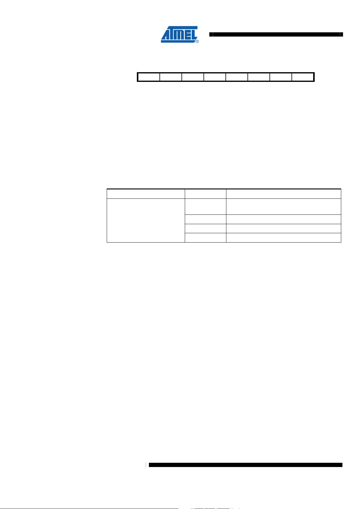
Bit 7 6 5 4 3 2 1 0
$3F ($5F) I T H S V N Z C SREG
Read/Write RW RW RW RW RW RW RW RW
Initial Value 0 0 0 0 0 0 0 0
• Bit 7 – I - Global Interrupt Enable
The global interrupt enable bit must be set (one) for the interrupts to be enabled. The
individual interrupt enable control is then performed in separate control registers. If the
global interrupt enable bit is cleared (zero), none of the interrupts are enabled
independent of the individual interrupt enable settings. The I-bit is cleared by hardware
after an interrupt has occurred, and is set by the RETI instruction to enable subsequent
interrupts.
• Bit 6 – T - Bit Copy Storage
The bit copy instructions BLD (Bit LoaD) and BST (Bit STore) use the T bit as source
and destination for the operated bit. A bit from a register in the register file can be
copied into T by the BST instruction, and a bit in T can be copied into a bit in a register
in the register file by the BLD instruction.
• Bit 5 – H - Half Carry Flag
The half carry flag H indicates a half carry in some arithmetic operations. See the
Instruction Set Description for detailed information.
• Bit 4 – S - Sign Bit
The S-bit is always an exclusive or between the negative flag N and the two's
complement overflow flag V. See the Instruction Set Description for detailed
information.
• Bit 3 – V - Two's Complement Overflow Flag
The two's complement overflow flag V supports two's complement arithmetics. See the
Instruction Set Description for detailed information.
• Bit 2 – N - Negative Flag
The negative flag N indicates a negative result after the different arithmetic and logic
operations. See the Instruction Set Description for detailed information.
• Bit 1 – Z - Zero Flag
The zero flag Z indicates a zero result after the different arithmetic and logic operations.
See the Instruction Set Description for detailed information.
8266A-MCU Wireless-12/09
• Bit 0 – C - Carry Flag
The carry flag C indicates a carry in an arithmetic or logic operation. See the Instruction
Set Description for detailed information. Note that the status register is not automatically
11
Page 12
ATmega128RFA1
stored when entering an interrupt routine and restored when returning from an interrupt
routine. This must be handled by software.
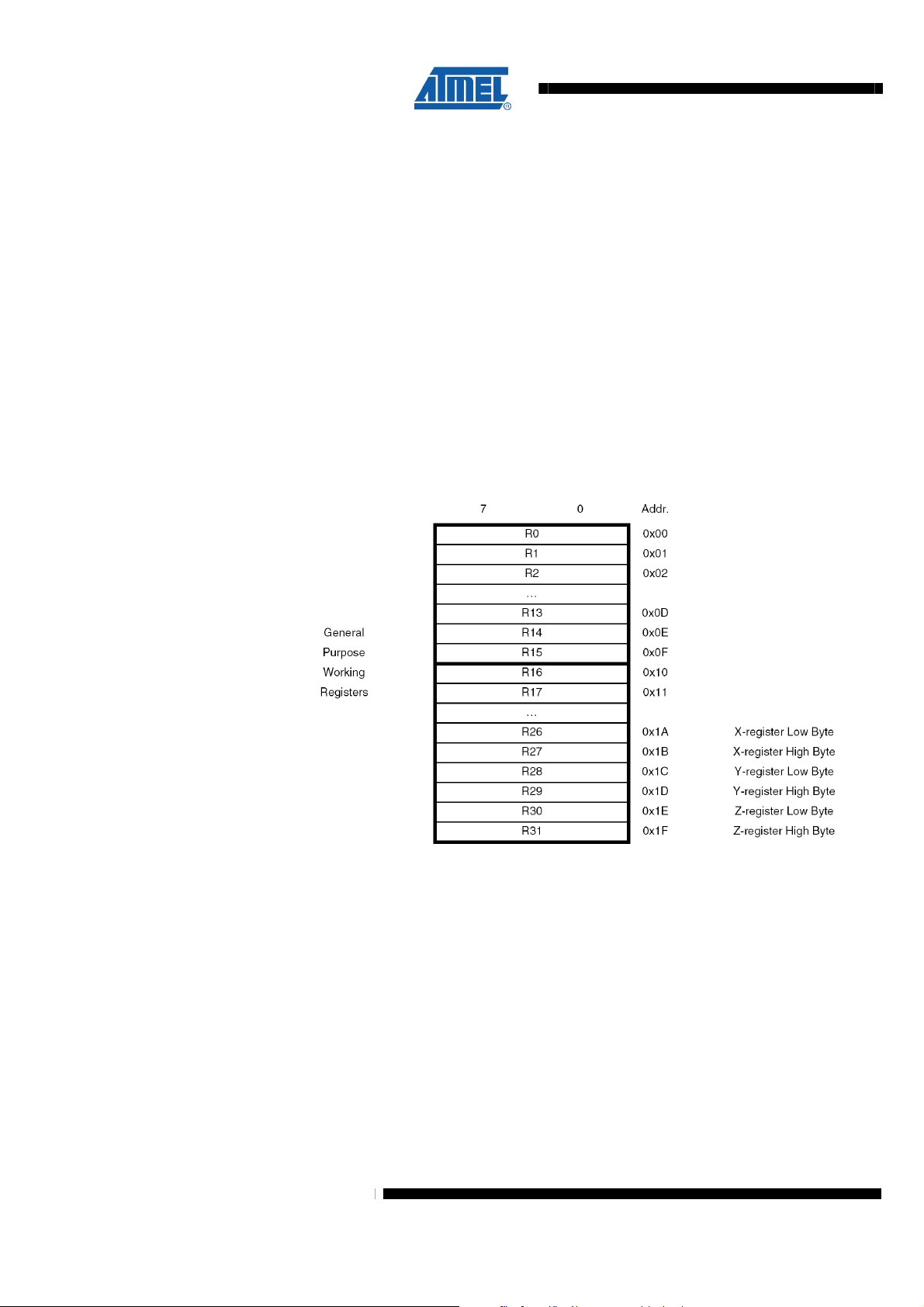
7.5 General Purpose Register File
The Register File is optimized for the AVR Enhanced RISC instruction set. In order to
achieve the required performance and flexibility, the following input/output schemes are
supported by the Register File:
• One 8-bit output operand and one 8-bit result input
• Two 8-bit output operands and one 8-bit result input
• Two 8-bit output operands and one 16-bit result input
• One 16-bit output operand and one 16-bit result input
Figure 7-1 below shows the structure of the 32 general purpose working registers in the
CPU.
Figure 7-1. AVR CPU General Purpose Working Registers
Most of the instructions operating on the Register File have direct access to all
registers, and most of them are single cycle instructions.
As shown in Figure 7-1 above on page 12, each register is also assigned a data
memory address, mapping them directly into the first 32 locations of the user Data
Space. Although not being physically implemented as SRAM locations, this memory
organization provides great flexibility in access of the registers, as the X-, Y- and Zpointer registers can be set to index any register in the file.
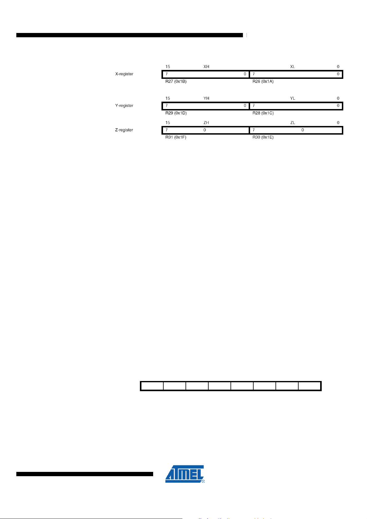
7.5.1 The X-register, Y-register, and Z-register
The registers R26...R31 have some added functions to their general purpose usage.
These registers are 16-bit address pointers for indirect addressing of the data space.
The three indirect address registers X, Y, and Z are defined as described in Figure 7-2
on page 13.
12
8266A-MCU Wireless-12/09
Page 13
ATmega128RFA1
7.6 Stack Pointer
Figure 7-2. The X-, Y-, Z-registers
In the different addressing modes these address registers have functions as fixed
displacement, automatic increment, and automatic decrement (see the instruction set
reference for details).
The Stack is mainly used for storing temporary data, for storing local variables and for
storing return addresses after interrupts and subroutine calls. The Stack Pointer
Register always points to the top of the Stack. Note that the Stack is implemented as
growing from higher memory locations to lower memory locations. This implies that a
Stack PUSH command decreases the Stack Pointer.
7.6.1 SPH – Stack Pointer High
The Stack Pointer points to the data SRAM Stack area where the Subroutine and
Interrupt Stacks are located. This Stack space in the data SRAM must be defined by
the program before any subroutine calls are executed or interrupts are enabled. The
Stack Pointer must be set to point above 0x0200. The initial value of the stack pointer is
the last address of the internal SRAM.
The Stack Pointer is decremented by one when data is pushed onto the Stack with the
PUSH instruction, and it is decremented by two when the return address is pushed onto
the Stack with subroutine call or interrupt. The Stack Pointer is incremented by one
when data is popped from the Stack with the POP instruction, and it is incremented by
two when data is popped from the Stack with return from subroutine RET or return from
interrupt RETI.
When the FLASH memory exceeds 128Kbyte one additional cycle is required. In this
case the Stack Pointer is decremented by three when the return address is pushed onto
the Stack with subroutine call or interrupt and is incremented by three when data is
popped from the Stack with return from subroutine RET or return from interrupt RETI.
Bit 7 6 5 4 3 2 1 0
$3E ($5E) SP15 SP14 SP13 SP12 SP11 SP10 SP9 SP8 SPH
Read/Write RW RW RW RW RW RW RW RW
Initial Value 0 0 1 0 0 0 0 1
8266A-MCU Wireless-12/09
The AVR Stack Pointer is implemented as two 8-bit registers SPL and SPH in the I/O
space. The number of bits actually used is implementation dependent. Note that the
data space in some implementations of the AVR architecture is so small that only SPL
is needed. In this case, the SPH Register will not be present.
• Bit 7:0 – SP15:8 - Stack Pointer High Byte
13
Page 14
ATmega128RFA1
7.6.2 SPL – Stack Pointer Low
Bit 7 6 5 4 3 2 1 0
$3D ($5D) SP7 SP6 SP5 SP4 SP3 SP2 SP1 SP0 SPL
Read/Write RW RW RW RW RW RW RW RW
Initial Value 1 1 1 1 1 1 1 1
The AVR Stack Pointer is implemented as two 8-bit registers SPL and SPH in the I/O
space. The number of bits actually used is implementation dependent. Note that the
data space in some implementations of the AVR architecture is so small that only SPL
is needed. In this case, the SPH Register will not be present.
• Bit 7:0 – SP7:0 - Stack Pointer Low Byte
7.6.3 RAMPZ – Extended Z-pointer Register for ELPM/SPM
Bit 7 6 5 4 3 2 1 0
$3B ($5B) Res5 Res4 Res3 Res2 Res1 Res0 RAMPZ1 RAMPZ0 RAMPZ
Read/Write RW RW RW RW RW RW RW RW
Initial Value 0 0 0 0 0 0 0 0
For ELPM/SPM instructions, the Z-pointer is a concatenation of RAMPZ, ZH, and ZL.
Note that LPM is not affected by the RAMPZ setting.
• Bit 7:2 – Res5:0 - Reserved
For compatibility with future devices, be sure to write these bits to zero.
• Bit 1:0 – RAMPZ1:0 - Extended Z-Pointer Value
These two bits represent the MSB's of the Z-Pointer.
Table 7-2 RAMPZ Register Bits
Register Bits Value Description
RAMPZ1:0 0 Default value of Z-pointer MSB's.
14
For ELPM/SPM instructions, the Z-pointer is a concatenation of RAMPZ, ZH, and ZL,
as shown in Figure 7-3 below. Note that LPM is not affected by the RAMPZ setting.
Figure 7-3. The Z-pointer used by ELPM and SPM
The actual number of bits is implementation dependent. Unused bits in an
implementation will always read as zero. For compatibility with future devices, be sure
to write these bits to zero.
8266A-MCU Wireless-12/09
Page 15
ATmega128RFA1
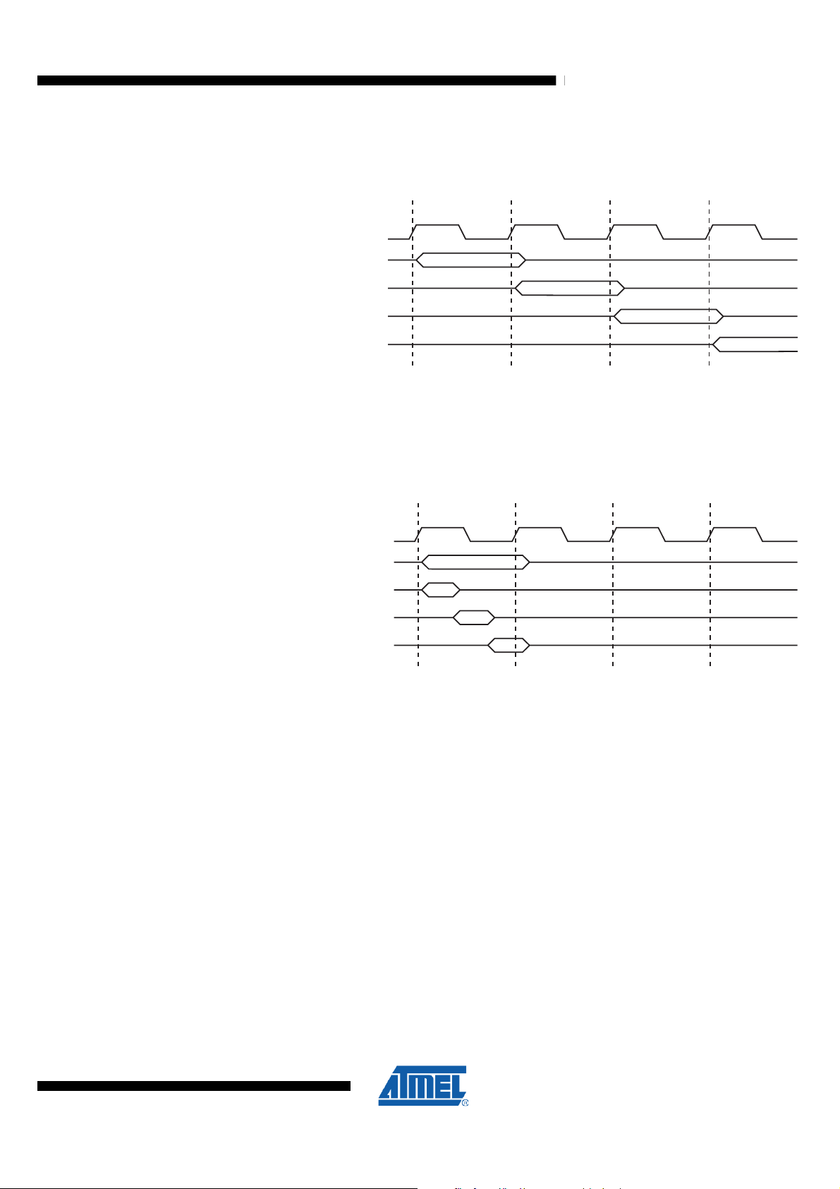
7.7 Instruction Execution Timing
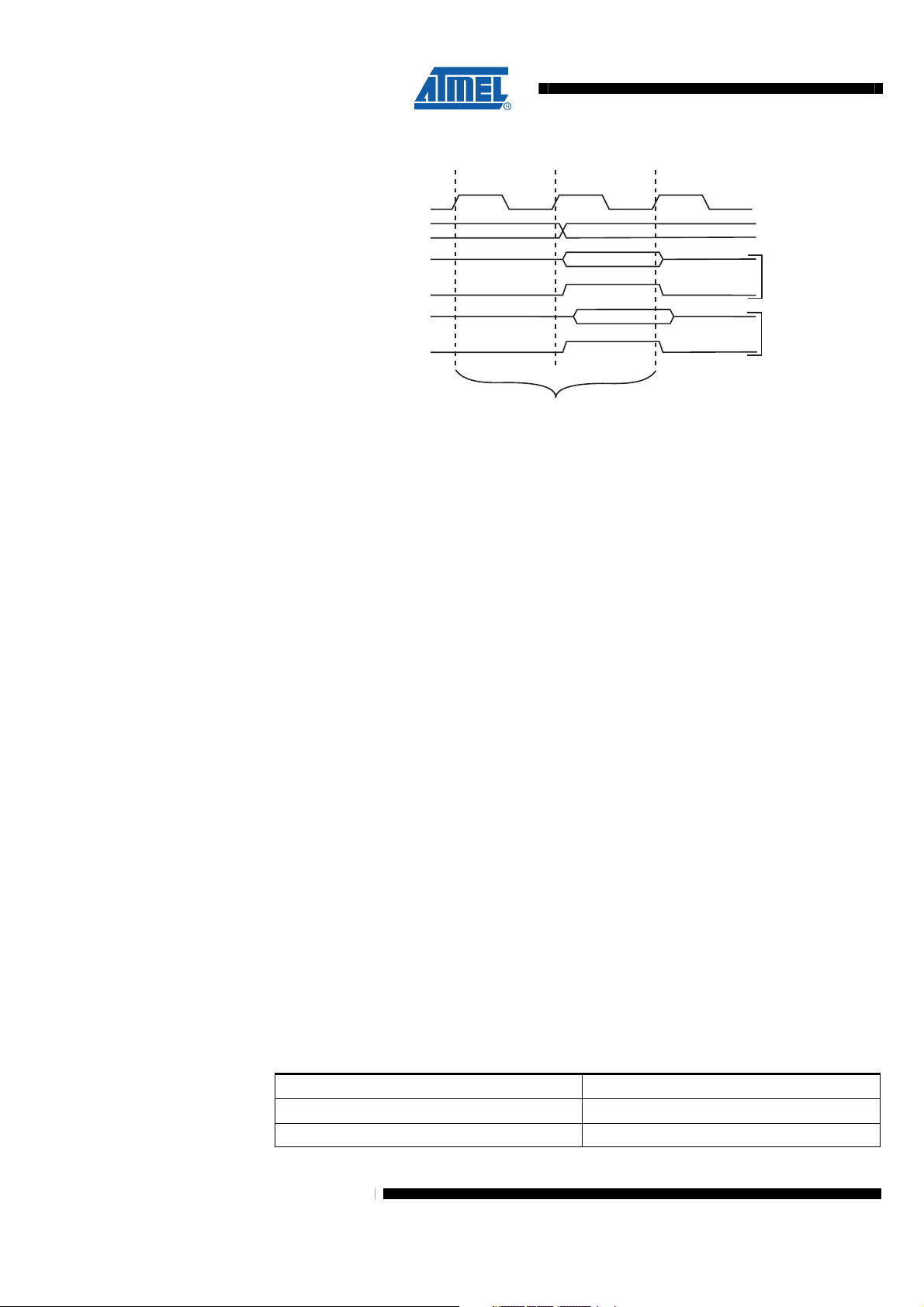
Figure 7-4. The Parallel Instruction Fetches and Instruction Executions
1st Instruction Fetch
1st Instruction Execute
2nd Instruction Fetch
2nd Instruction Execute
3rd Instruction Fetch
3rd Instruction Execute
4th Instruction Fetch
Figure 7-5 below shows the internal timing concept for the Register File. In a single
clock cycle an ALU operation using two register operands is executed, and the result is
stored back to the destination register.
Figure 7-5. Single Cycle ALU operation
clk
CPU
T1 T2 T3 T4
T1 T2 T3 T4
Total Execution Time
Register Operands Fetch
ALU Operation Execute
Result Write Back
7.8 Reset and Interrupt Handling
The AVR provides several different interrupt sources. These interrupts and the separate
Reset Vector each have a separate program vector in the program memory space. All
interrupts are assigned individual enable bits which must be written logic one together
with the Global Interrupt Enable bit in the Status Register in order to enable the
interrupt. Depending on the Program Counter value, interrupts may be automatically
disabled when Boot Lock bits BLB02 or BLB12 are programmed. This feature improves
software security. See the section "Memory Programming" on page 464 for details.
The lowest addresses in the program memory space are by default defined as the
Reset and Interrupt Vectors. The complete list of vectors is shown in "Interrupts" on
page 211. The list also determines the priority levels of the different interrupts. The
lower the address the higher is the priority level. RESET has the highest priority, and
next is INT0 – the External Interrupt Request 0. The Interrupt Vectors can be moved to
the start of the Boot Flash section by setting the IVSEL bit in the MCU Control Register
(MCUCR). Refer to "Interrupts" on page 211 for more information. The Reset Vector
can also be moved to the start of the Boot Flash section by programming the
BOOTRST Fuse, see "Memory Programming" on page 464.
clk
CPU
8266A-MCU Wireless-12/09
When an interrupt occurs, the Global Interrupt Enable I-bit is cleared and all interrupts
are disabled. The user software can write logic one to the I-bit to enable nested
15
Page 16

ATmega128RFA1
interrupts. All enabled interrupts can then interrupt the current interrupt routine. The I-bit
is automatically set when a Return from Interrupt instruction – RETI – is executed.
There are basically two types of interrupts. The first type is triggered by an event that
sets the Interrupt Flag. For these interrupts, the Program Counter is vectored to the
actual Interrupt Vector in order to execute the interrupt handling routine, and hardware
clears the corresponding Interrupt Flag. Interrupt Flags can also be cleared by writing a
logic one to the flag bit position(s) to be cleared. If an interrupt condition occurs while
the corresponding interrupt enable bit is cleared, the Interrupt Flag will be set and
remembered until the interrupt is enabled, or the flag is cleared by software. Similarly, if
one or more interrupt conditions occur while the Global Interrupt Enable bit is cleared,
the corresponding Interrupt Flag(s) will be set and remembered until the Global
Interrupt Enable bit is set, and will then be executed by order of priority.
The second type of interrupts will trigger as long as the interrupt condition is present.
These interrupts do not necessarily have Interrupt Flags. If the interrupt condition
disappears before the interrupt is enabled, the interrupt will not be triggered.
When the AVR exits from an interrupt, it will always return to the main program and
execute one more instruction before any pending interrupt is served.
Note that the Status Register is not automatically stored when entering an interrupt
routine, nor restored when returning from an interrupt routine. This must be handled by
software.
When using the CLI instruction to disable interrupts, the interrupts will be immediately
disabled. No interrupt will be executed after the CLI instruction, even if it occurs
simultaneously with the CLI instruction. The following example shows how this can be
used to avoid interrupts during the timed EEPROM write sequence.
Assembly Code Example
in r16, SREG ; store SREG value
cli ; disable interrupts during timed sequence
sbi EECR, EEMPE ; start EEPROM write
sbi EECR, EEPE
out SREG, r16 ; restore SREG value (I-bit)
C Code Example
char cSREG;
cSREG = SREG; /* store SREG value */
/* disable interrupts during timed sequence */
__disable_interrupt();
EECR |= (1<<EEMPE); /* start EEPROM write */
EECR |= (1<<EEPE);
SREG = cSREG; /* restore SREG value (I-bit) */
When using the SEI instruction to enable interrupts, the instruction following SEI will be
executed before any pending interrupts, as shown in this example.
Assembly Code Example
sei ; set Global Interrupt Enable
sleep; enter sleep, waiting for interrupt
16
8266A-MCU Wireless-12/09
Page 17

ATmega128RFA1
7.8.1 Interrupt Response Time
Assembly Code Example
; note: will enter sleep before any pending
; interrupt(s)
C Code Example
__enable_interrupt(); /* set Global Interrupt Enable */
__sleep(); /* enter sleep, waiting for interrupt */
/* note: will enter sleep before any pending interrupt(s) */
The interrupt execution response for all the enabled AVR interrupts is five clock cycles
minimum. After five clock cycles the program vector address for the actual interrupt
handling routine is executed. During these five clock cycle period, the Program Counter
is pushed onto the Stack. The vector is normally a jump to the interrupt routine, and this
jump takes three clock cycles. If an interrupt occurs during execution of a multi-cycle
instruction, this instruction is completed before the interrupt is served. If an interrupt
occurs when the MCU is in sleep mode, the interrupt execution response time is
increased by five clock cycles. This increase comes in addition to the start-up time from
the selected sleep mode.
A return from an interrupt handling routine takes five clock cycles. During these five
clock cycles, the Program Counter (three bytes) is popped back from the Stack, the
Stack Pointer is incremented by three, and the I-bit in SREG is set.
8266A-MCU Wireless-12/09
17
Page 18

ATmega128RFA1
8 AVR Memories
This section describes the different memories in the ATmega128RFA1. The AVR
architecture has two main memory spaces, the Data Memory and the Program Memory
space. In addition, the ATmega128RFA1 features an EEPROM Memory for data
storage. All three memory spaces are linear and regular.
8.1 In-System Reprogrammable Flash Program Memory
The ATmega128RFA1 contains 128K bytes On-chip In-System Reprogrammable Flash
memory for program storage, see
32 bits wide, the Flash is 16 bit wide. For software security, the Flash Program memory
space is divided into two sections, Boot Program section and Application Program
section.
The Flash memory has an endurance of at least 2000 write/erase cycles. The
ATmega128RFA1 Program Counter (PC) is 16 bits wide, thus addressing the required
program memory locations. The operation of Boot Program section and associated
Boot Lock bits for software protection are described in detail in "Boot Loader Support –
Read-While-Write Self-Programming" on page 450. "Memory Programming" on page
464 contains a detailed description on Flash data serial downloading using the SPI pins
or the JTAG interface.
Constant tables can be allocated within the entire program memory address space (see
the LPM – Load Program Memory instruction description and ELPM – Extended Load
Program Memory instruction description).
Timing diagrams for instruction fetch and execution are presented in "Instruction
Execution Timing" on page 15.
Figure 8-6 below. Since all AVR instructions are 16 or
Figure 8-6. Program Flash Memory Map
Program Memory
8.2 SRAM Data Memory
18
Application Flash Section
$0000
Boot Flash Section
Figure 8-7 on page 19 shows how the ATmega128RFA1 SRAM Memory is organized.
The ATmega128RFA1 is a complex microcontroller with more peripheral units than can
be supported within the 64 location reserved in the Opcode for the IN and OUT
instructions. For the Extended I/O space from $060 – $1FF in SRAM, only the
ST/STS/STD and LD/LDS/LDD instructions can be used.
The first Data Memory locations address both the Register File, the I/O Memory,
Extended I/O Memory, and the internal data SRAM. The first 32 locations address the
Register file, the next 64 location the standard I/O Memory, then 416 locations of
Extended I/O memory and the following locations address the internal data SRAM.
8266A-MCU Wireless-12/09
Page 19
ATmega128RFA1
The five different addressing modes for the data memory cover: Direct, Indirect with
Displacement, Indirect, Indirect with Pre-decrement, and Indirect with Post-increment.
In the Register file, registers R26 to R31 feature the indirect addressing pointer
registers.
The direct addressing reaches the entire data space.
The Indirect with Displacement mode reaches 63 address locations from the base
address given by the Y- or Z-register.
When using register indirect addressing modes with automatic pre-decrement and postincrement, the address registers X, Y, and Z are decremented or incremented.
The 32 general purpose working registers, 64 I/O registers, and the internal data SRAM
in the ATmega128RFA1 are all accessible through all these addressing modes. The
Register File is described in "General Purpose Register File" on page 12.
Figure 8-7. Data Memory Map
Data Memory
32 Registers
64 I/O Registers
416 Ext I/O Reg.
Internal SRAM
(16K x 8)
$0000 - $001F
$0020 - $005F
$0060 - $01FF
$0200
$41FF
8.2.1 Data Memory Access Times
This section describes the general access timing concepts for internal memory access.
Access to the internal data SRAM is performed in two clk
Figure 8-8 on page 20.
8266A-MCU Wireless-12/09
$FFFF
CPU
cycles as described in
19
Page 20
ATmega128RFA1
Figure 8-8. On-Chip Data SRAM Access Cycles
T1 T2 T3
clk
CPU
Address
Data
WR
Compute Address
Address valid
Data
RD
Write
Read
8.3 EEPROM Data Memory
The ATmega128RFA1 contains 4Kbyte of data EEPROM memory. It is organized as a
separate data space, in which single bytes can be read and written. The EEPROM has
an endurance of at least 2000 write/erase cycles. The access between the EEPROM
and the CPU is described in the following, specifying the EEPROM Address Registers,
the EEPROM Data Register, and the EEPROM Control Register.
For a detailed description of SPI, JTAG and Parallel data downloading to the EEPROM,
see "Serial Downloading" on page 477, "Programming via the JTAG Interface" on page
481, and "Programming the EEPROM" on page 491 respectively.
8.3.1 EEPROM Read Write Access
The EEPROM Access Registers are accessible in the I/O space, see "EEPROM
Register Description" on page 23.
The write access time for the EEPROM is given in Table 8-3 below. A self-timing
function, however, lets the user software detect when the next byte can be written. If the
user code contains instructions that write the EEPROM, some precautions must be
taken. In heavily filtered power supplies, DVDD is likely to rise or fall slowly on powerup/down. This causes the device for some period of time to run at a voltage lower than
specified as minimum for the clock frequency used. See "Preventing EEPROM
Corruption" on page 22 for details on how to avoid problems in these situations.
Memory Access Instruction
Next Instruction
20
In order to prevent unintentional EEPROM writes, a specific write procedure must be
followed. See the description of the EEPROM Control Register for details on this,
"EEPROM Register Description" on page 23.
When the EEPROM is read, the CPU is halted for four clock cycles before the next
instruction is executed. When the EEPROM is written, the CPU is halted for two clock
cycles before the next instruction is executed.
The calibrated Oscillator is used to time the EEPROM accesses. The following table
lists the typical programming time for EEPROM access from the CPU.
Table 8-3. EEPROM Programming Time
Symbol Typical Programming time
EEPROM write (from CPU) 4ms
EEPROM erase (from CPU) 8ms
8266A-MCU Wireless-12/09
Page 21

ATmega128RFA1
The following code examples show one assembly and one C function for writing to the
EEPROM. The examples assume that interrupts are controlled (e.g. by disabling
interrupts globally) so that no interrupts will occur during execution of these functions.
The examples also assume that no Flash Boot Loader is present in the software. If such
code is present, the EEPROM write function must also wait for any ongoing SPM
command to finish.
Assembly Code Example
EEPROM_write:
; Wait for completion of previous write
sbic EECR,EEPE
rjmp EEPROM_write
; Set up address (r18:r17) in address register
out EEARH, r18
out EEARL, r17
; Write data (r16) to Data Register
out EEDR,r16
; Write logical one to EEMPE
sbi EECR,EEMPE
; Start eeprom write by setting EEPE
sbi EECR,EEPE
ret
C Code Example
void EEPROM_write(unsigned int uiAddress, unsigned char ucData)
{
/* Wait for completion of previous write */
while(EECR & (1<<EEPE))
;
/* Set up address and Data Registers */
EEAR = uiAddress;
EEDR = ucData;
/* Write logical one to EEMPE */
EECR |= (1<<EEMPE);
/* Start eeprom write by setting EEPE */
EECR |= (1<<EEPE);
}
8266A-MCU Wireless-12/09
The next code examples show assembly and C functions for reading the EEPROM. The
examples assume that interrupts are controlled so that no interrupts will occur during
execution of these functions.
Assembly Code Example
EEPROM_read:
; Wait for completion of previous write
21
Page 22

ATmega128RFA1
Assembly Code Example
sbic EECR,EEPE
rjcmp EEPROM_read
; Set up address (r18:r17) in address register
out EEARH, r18
out EEARL, r17
; Start eeprom read by writing EERE
sbi EECR,EERE
; Read data from Data Register
in r16,EEDR
ret
C Code Example
unsigned char EEPROM_read(unsigned int uiAddress)
{
/* Wait for completion of previous write */
while(EECR & (1<<EEPE))
;
/* Set up address register */
EEAR = uiAddress;
/* Start eeprom read by writing EERE */
EECR |= (1<<EERE);
/* Return data from Data Register */
return EEDR;
}
8.3.2 Preventing EEPROM Corruption
During periods of low DEVDD, the EEPROM data can be corrupted because the supply
voltage is too low for the CPU and the EEPROM to operate properly. These issues are
the same as for board level systems using EEPROM, and the same design solutions
should be applied.
An EEPROM data corruption can be caused by two situations when the voltage is too
low. First, a regular write sequence to the EEPROM requires a minimum voltage to
operate correctly. Secondly, the CPU itself can execute instructions incorrectly, if the
supply voltage is too low.
EEPROM data corruption can easily be avoided by following this design
recommendation:
Keep the AVR RESET active (low) during periods of insufficient power supply voltage.
This can be done by enabling the internal Brown-out Detector (BOD). If the detection
level of the internal BOD does not match the needed detection level, an external low
VCC reset Protection circuit can be used. If a reset occurs while a write operation is in
progress, the write operation will be completed provided that the power supply voltage
is sufficient.
22
8266A-MCU Wireless-12/09
Page 23

ATmega128RFA1
8.4 EEPROM Register Description
8.4.1 EEARH – EEPROM Address Register High Byte
Bit 7 6 5 4 3 2 1 0
$22 ($42) Res3 Res2 Res1 Res0 EEAR11 EEAR10 EEAR9 EEAR8 EEARH
Read/Write R R R R RW RW RW RW
Initial Value 0 0 0 0 X X X X
The EEPROM Address Registers EEARH and EEARL specify the EEPROM address in
the 4K bytes EEPROM space. The EEPROM data bytes are addressed linearly
between 0 and 4096. The initial value of EEAR is undefined. A proper value must be
written before the EEPROM may be accessed.
• Bit 7:4 – Res3:0 - Reserved
• Bit 3:0 – EEAR11:8 - EEPROM Address
8.4.2 EEARL – EEPROM Address Register Low Byte
Bit 7 6 5 4 3 2 1 0
$21 ($41) EEAR7 EEAR6 EEAR5 EEAR4 EEAR3 EEAR2 EEAR1 EEAR0 EEARL
Read/Write RW RW RW RW RW RW RW RW
Initial Value X X X X X X X X
The EEPROM Address Registers EEARH and EEARL specify the EEPROM address in
the 4K bytes EEPROM space. The EEPROM data bytes are addressed linearly
between 0 and 4096. The initial value of EEAR is undefined. A proper value must be
written before the EEPROM may be accessed.
• Bit 7:0 – EEAR7:0 - EEPROM Address
8.4.3 EEDR – EEPROM Data Register
Bit 7 6 5 4 3 2 1 0
$20 ($40) EEDR7:0 EEDR
Read/Write RW RW RW RW RW RW RW RW
Initial Value 0 0 0 0 0 0 0 0
For the EEPROM write operation, the EEDR Register contains the data to be written to
the EEPROM in the address given by the EEAR Register. For the EEPROM read
operation, the EEDR contains the data read out from the EEPROM at the address given
by EEAR.
8266A-MCU Wireless-12/09
• Bit 7:0 – EEDR7:0 - EEPROM Data
23
Page 24
ATmega128RFA1
8.4.4 EECR – EEPROM Control Register
Bit 7 6 5 4 3 2 1 0
$1F ($3F) Res1 Res0 EEPM1 EEPM0 EERIE EEMPE EEPE EERE EECR
Read/Write R R RW RW RW RW RW RW
Initial Value 0 0 X X 0 0 X 0
• Bit 7:6 – Res1:0 - Reserved
• Bit 5:4 – EEPM1:0 - EEPROM Programming Mode
The EEPROM Programming mode bit setting defines which programming action will be
triggered when writing EEPE. It is possible to program data in one atomic operation
(erase the old value and program the new value) or to split the Erase and Write
operations in two different operations. The Programming times for the different modes
are shown in the following table. While EEPE is set, any write to EEPM1:0 will be
ignored. During reset, the EEPM1:0 bits will be reset to 0 unless the EEPROM is busy
programming.
Table 8-4 EEPM Register Bits
Register Bits Value Description
EEPM1:0
• Bit 3 – EERIE - EEPROM Ready Interrupt Enable
Writing EERIE to one enables the EEPROM Ready Interrupt if the I bit in SREG is set.
Writing EERIE to zero disables the interrupt. The EEPROM Ready interrupt generates a
constant interrupt when EEPE is cleared.
• Bit 2 – EEMPE - EEPROM Master Write Enable
The EEMPE bit determines whether setting EEPE to one causes the EEPROM to be
written. When EEMPE is set, setting EEPE within four clock cycles will write data to the
EEPROM at the selected address If EEMPE is zero, setting EEPE will have no effect.
When EEMPE has been written to one by software, hardware clears the bit to zero after
four clock cycles. See the description of the EEPE bit for an EEPROM write procedure.
0x00 Erase and Write in one operation (Atomic
Operation)
0x01 Erase only
0x02 Write only
0x03 Reserved for future use
24
• Bit 1 – EEPE - EEPROM Programming Enable
The EEPROM Write Enable Signal EEPE is the write strobe to the EEPROM. When
address and data are correctly set up, the EEPE bit must be written to one to write the
value into the EEPROM. The EEMPE bit must be written to one before a logical one is
written to EEPE, otherwise no EEPROM write takes place. The following procedure
should be adopted when writing the EEPROM (the order of steps 3 and 4 is not
essential):
1. Wait until EEPE becomes zero.
2. Wait until SPMEN in SPMCSR becomes zero.
3. Write new EEPROM address to EEAR (optional).
4. Write new EEPROM data to EEDR (optional).
5. Write a logical one to the EEMPE bit while writing a zero to EEPE in EECR.
6. Within four clock cycles after setting EEMPE, write a logical one to EEPE.
8266A-MCU Wireless-12/09
Page 25

ATmega128RFA1
The EEPROM can not be programmed during a CPU write to the Flash memory. The
software must check that the Flash programming is completed before initiating a new
EEPROM write. Step 2 is only relevant if the software contains a Boot Loader allowing
the CPU to program the Flash. If the Flash is never being updated by the CPU, step 2
can be omitted.
Caution: an interrupt between step 5 and step 6 will make the write cycle fail, since the
EEPROM Master Write Enable will time-out. If an interrupt routine accessing the
EEPROM is interrupting another EEPROM access, the EEAR or EEDR Register will be
modified, causing the interrupted EEPROM access to fail. It is recommended to have
the Global Interrupt Flag cleared during all steps to avoid these problems.
When the write access time has elapsed, the EEPE bit is cleared by hardware. The
user software can poll this bit and wait for a zero before writing the next byte. When
EEPE has been set, the CPU is halted for two cycles before the next instruction is
executed.
• Bit 0 – EERE - EEPROM Read Enable
The EEPROM Read Enable Signal EERE is the read strobe to the EEPROM. When the
correct address is set up in the EEAR Register, the EERE bit must be written to a logic
one to trigger the EEPROM read. The EEPROM read access takes one instruction and
the requested data is available immediately. When the EEPROM is read, the CPU is
halted for four cycles before the next instruction is executed. The user should poll the
EEPE bit before starting the read operation. If a write operation is in progress, it is
neither possible to read the EEPROM nor to change the EEAR Register.
8.5 I/O Memory
The Input/Output (I/O) space definition of the ATmega128RFA1 is shown in "Register
Summary" on page 496.
All ATmega128RFA1 I/Os and peripherals are placed in the I/O space. All I/O locations
may be accessed by the LD/LDS/LDD and ST/STS/STD instructions, transferring data
between the 32 general purpose working registers and the I/O space. I/O Registers
within the address range 0x00 – 0x1F are directly bit-accessible using the SBI and CBI
instructions. In these registers, the value of single bits can be checked by using the
SBIS and SBIC instructions. Refer to the AVR instruction set for more details. When
using the I/O specific commands IN and OUT, the I/O addresses 0x00 – 0x3F must be
used. When addressing I/O Registers as data space using LD and ST instructions,
0x20 must be added to these addresses. The ATmega128RFA1 is a complex
microcontroller with more peripheral units than can be supported within the 64 location
reserved in Opcode for the IN and OUT instructions. For the Extended I/O space from
0x60 – 0x1FF in SRAM, only the ST/STS/STD and LD/LDS/LDD instructions can be
used.
For compatibility with future devices, reserved bits may not be modified. Reserved
registers and I/O memory addresses should never be written.
Some of the Status Flags are cleared by writing a logical one to them. Note that, unlike
most other AVRs, the CBI and SBI instructions will only operate on the specified bit,
and can therefore be used on registers containing such Status Flags. The CBI and SBI
instructions work with registers 0x00 to 0x1F only.
The control registers of I/O and peripherals are explained in later sections.
8266A-MCU Wireless-12/09
25
Page 26

ATmega128RFA1
8.6 General Purpose I/O Registers
The ATmega128RFA1 contains three General Purpose I/O Registers. These registers
can be used for storing any information, and they are particularly useful for storing
global variables and Status Flags. General Purpose I/O Registers within the address
range 0x00 – 0x1F are directly bit-accessible using the SBI, CBI, SBIS, and SBIC
instructions.
8.6.1 GPIOR0 – General Purpose IO Register 0
Bit 7 6 5 4 3 2 1 0
$1E ($3E) GPIOR07:00 GPIOR0
Read/Write RW RW RW RW RW RW RW RW
Initial Value 0 0 0 0 0 0 0 0
The three General Purpose I/O Registers can be used for storing any information.
• Bit 7:0 – GPIOR07:00 - General Purpose I/O Register 0 Value
8.6.2 GPIOR1 – General Purpose IO Register 1
Bit 7 6 5 4 3 2 1 0
$2A ($4A) GPIOR17:10 GPIOR1
Read/Write RW RW RW RW RW RW RW RW
Initial Value 0 0 0 0 0 0 0 0
The three General Purpose I/O Registers can be used for storing any information.
• Bit 7:0 – GPIOR17:10 - General Purpose I/O Register 1 Value
8.6.3 GPIOR2 – General Purpose I/O Register 2
Bit 7 6 5 4 3 2 1 0
$2B ($4B) GPIOR27:20 GPIOR2
Read/Write RW RW RW RW RW RW RW RW
Initial Value 0 0 0 0 0 0 0 0
The three General Purpose I/O Registers can be used for storing any information.
• Bit 7:0 – GPIOR27:20 - General Purpose I/O Register 2 Value
8.7 Other Port Registers
The inherited control registers of missing ports located in the I/O space are kept in the
ATmega128RFA1. They can be used as general purpose I/O registers for storing any
information. Registers placed in the address range 0x00 – 0x1F are directly bitaccessible using the SBI, CBI, SBIS and SBIC instructions.
26
8266A-MCU Wireless-12/09
Page 27

ATmega128RFA1
8.7.1 PORTA – Port A Data Register
Bit 7 6 5 4 3 2 1 0
$02 ($22) PORTA7:0 PORTA
Read/Write RW RW RW RW RW RW RW RW
Initial Value 0 0 0 0 0 0 0 0
The PORTA register can be used as a General Purpose I/O Register for storing any
information.
• Bit 7:0 – PORTA7:0 - Port A Data Register Value
8.7.2 DDRA – Port A Data Direction Register
Bit 7 6 5 4 3 2 1 0
$01 ($21) DDA7 DDA6 DDA5 DDA4 DDA3 DDA2 DDA1 DDA0 DDRA
Read/Write RW RW RW RW RW RW RW RW
Initial Value 0 0 0 0 0 0 0 0
The DDRA register can be used as a General Purpose I/O Register for storing any
information.
• Bit 7:0 – DDA7:0 - Port A Data Direction Register Value
8.7.3 PINA – Port A Input Pins Address
Bit 7 6 5 4 3 2 1 0
$00 ($20) PINA7:0 PINA
Read/Write RW RW RW RW RW RW RW RW
Initial Value 0 0 0 0 0 0 0 0
The PINA register is reserved for interal use and cannot be used as a General Purpose
I/O Register.
• Bit 7:0 – PINA7:0 - Port A Input Pins
8.7.4 PORTC – Port C Data Register
Bit 7 6 5 4 3 2 1 0
$08 ($28) PORTC7:0 PORTC
Read/Write RW RW RW RW RW RW RW RW
Initial Value 0 0 0 0 0 0 0 0
The PORTC register can be used as a General Purpose I/O Register for storing any
information.
• Bit 7:0 – PORTC7:0 - Port C Data Register Value
8266A-MCU Wireless-12/09
27
Page 28

ATmega128RFA1
8.7.5 DDRC – Port C Data Direction Register
Bit 7 6 5 4 3 2 1 0
$07 ($27) DDC7 DDC6 DDC5 DDC4 DDC3 DDC2 DDC1 DDC0 DDRC
Read/Write RW RW RW RW RW RW RW RW
Initial Value 0 0 0 0 0 0 0 0
The DDRC register can be used as a General Purpose I/O Register for storing any
information.
• Bit 7:0 – DDC7:0 - Port C Data Direction Register Value
8.7.6 PINC – Port C Input Pins Address
Bit 7 6 5 4 3 2 1 0
$06 ($26) PINC7:0 PINC
Read/Write R R R R R R R R
Initial Value 0 0 0 0 0 0 0 0
The PINC register is reserved for interal use and cannot be used as a General Purpose
I/O Register.
• Bit 7:0 – PINC7:0 - Port C Input Pins
28
8266A-MCU Wireless-12/09
Page 29

ATmega128RFA1
9 Low-Power 2.4 GHz Transceiver
9.1 Features
• High performance RF-CMOS 2.4 GHz radio transceiver targeted for IEEE
802.15.4™, ZigBee™, IPv6 / 6LoWPAN, RF4CE, SP100, WirelessHART™ and
ISM applications
• Outstanding link budget (103.5 dB):
o Receiver sensitivity -100 dBm
o Programmable output power from -17 dBm up to +3.5 dBm
• Ultra-low current consumption:
o TRX_OFF = 0.4 mA
o RX_ON = 12.5 mA
o BUSY_TX = 14.5 mA (at max. transmit power of +3.5 dBm)
• Optimized for low BoM cost and ease of production:
o Few external components necessary (crystal, capacitors and
o Excellent ESD robustness
• Easy to use interface:
o Registers and frame buffer access from software
o Dedicated radio transceiver interrupts
• Radio transceiver features:
o 128 byte FIFO (SRAM) for data buffering
o Integrated RX/TX switch
o Fully integrated, fast settling PLL to support frequency hopping
o Battery monitor
o Fast wake-up time < 0.25 ms
• Special IEEE 802.15.4 2006 hardware support:
o FCS computation and clear channel assessment (CCA)
o RSSI measurement, energy detection and link quality indication
• MAC hardware accelerator:
o Automated acknowledgement, CSMA-CA and frame
o Automatic address filtering
o Automated FCS check
• Extended Feature Set Hardware Support:
o AES 128 bit hardware accelerator
o RX/TX indication (external RF front-end control)
o RX antenna diversity
o Supported PSDU data rates: 250 kb/s, 500 kb/s, 1 Mb/s and 2 Mb/s
o True random number generation for security applications
• Compliant to IEEE 802.15.4-2006, IEEE 802.15.4-2003 and RF4CE
• Compliant to EN 300 328/440, FCC-CFR-47 Part 15, ARIB STD-66, RSS-210
antenna)
retransmission
8266A-MCU Wireless-12/09
29
Page 30
ATmega128RFA1
The ATmega128RFA1 features a low-power 2.4 GHz radio transceiver designed for
industrial and consumer ZigBee/IEEE 802.15.4, 6LoWPAN, RF4CE and high data rate
2.4 GHz ISM band applications. The radio transceiver is a true peripheral block of the
AVR microcontroller. All RF-critical components except the antenna, crystal and decoupling capacitors are integrated on-chip. Therefore, the ATmega128RFA1 is
particularly suitable for applications like:
• 2.4 GHz IEEE 802.15.4 and ZigBee systems
• 6LoWPAN and RF4CE systems
• Wireless sensor networks
• Industrial control, sensing and automation (SP100, WirelessHART)
• Residential and commercial automation
• Health care
• Consumer electronics
• PC peripherals
9.2 General Circuit Description
This radio transceiver is part of a system-on-chip solution with an AVR® microcontroller.
It comprises a complex peripheral component containing the analog radio, digital
modulation and demodulation including time and frequency synchronization and data
buffering. The number of external components for the transceiver operation is
minimized such that only the antenna, the crystal and decoupling capacitors are
required. The bidirectional differential antenna pins (RFP, RFN) are used for
transmission and reception, thus no external antenna switch is needed.
The ATmega128RFA1 block diagram is shown in
Figure 9-9. Transceiver Block Diagram
DIG3/4
RFP
RFN
LNA
AD
DIG1/2
Analog Domain Digital Domain
ext. PA and Power
Control
PLL PA
PPF BPF Limiter
Antenna Diversity
Figure 9-9 below.
XTAL1
XOSC
XTAL2
AVREG
Configuration Registers
TX Data
FTN, BATMON
AGC
RX
ADC
RSSI
TX BBP
Frame
Buffer
RX BBP
DVREG
µC
Interface
AES
Control Logic
Data
Interrupts
Address
Control
30
8266A-MCU Wireless-12/09
Page 31

ATmega128RFA1
The received RF signal at pins RFN and RFP is differentially fed through the low-noise
amplifier (LNA) to the RF filter (PPF) to generate a complex signal, driving the
integrated channel filter (BPF). The limiting amplifier provides sufficient gain to drive the
succeeding analog-to-digital converter (RX ADC) and generates a digital RSSI signal.
The RX ADC output signal is sampled by the digital base band receiver (RX BBP).
The transmit modulation scheme is offset-QPSK (O-QPSK) with half-sine pulse shaping
and 32-length block coding (spreading) according to [1] on page 100 and [2] on page
100. The modulation signal is generated in the digital transmitter (TX BBP) and applied
to the fractional-N frequency synthesis (PLL), to ensure the coherent phase modulation
required for demodulation of O-QPSK signals. The frequency-modulated signal is fed to
the power amplifier (PA).
A differential pin pair DIG3/DIG4 can be enabled to control an external RF front-end.
The two on-chip low-dropout voltage regulators (A|DVREG) provide the analog and
digital 1.8V supply.
An internal 128-byte RAM for RX and TX (Frame Buffer) buffers the data to be
transmitted or received.
The configuration of the reading and writing of the Frame Buffer is controlled via the
microcontroller interface.
The transceiver further contains comprehensive hardware-MAC support (Extended
Operating Mode) and a security engine (AES) to improve the overall system power
efficiency and timing. The 128-bit AES engine can be accessed in parallel to all PHY
operational transactions and states using the microcontroller interface, except during
transceiver power down state.
For applications not necessarily targeting IEEE 802.15.4 compliant networks, the radio
transceiver also supports alternative data rates up to 2 Mb/s.
For long-range applications or to improve the reliability of an RF connection the RF
performance can further be improved by using an external RF front-end or Antenna
Diversity. Both operation modes are supported by the radio transceiver with dedicated
control pins without the interaction of the microcontroller.
Additional features of the Extended Feature Set, see section "Radio Transceiver
Extended Feature Set" on page 85, are provided to simplify the interaction between
radio transceiver and microcontroller.
9.3 Transceiver to Microcontroller Interface
This section describes the internal Interface between the transceiver module and the
microcontroller. Unlike all other AVR I/O modules, the transceiver module can operate
asynchronously to the controller. The transceiver requires an accurate 16MHz crystal
clock for operation, but the controller can run at any frequency within its operating limits.
9.3.1 Transceiver Configuration and Data Access
9.3.1.1 Register Access
All transceiver registers are mapped into I/O space of the controller. Due to the
asynchronous interface a register access can take up to three transceiver clock cycles.
Depending on the controller clock speed, program execution wait cycles are generated.
That means if the controller runs with about 16MHz or faster, at least three wait cycles
are generated, but if the controller runs with about 4MHz, no wait cycles are inserted. A
8266A-MCU Wireless-12/09
31
Page 32

ATmega128RFA1
9.3.1.2 Frame Buffer Access
register access is only possible, if the transceiver clock is available. Therefore the
transceiver must be enabled (PRR1 Register) and not in SLEEP state.
The 128-byte Frame Buffer can hold the PHY service data unit (PSDU) data of one
IEEE 802.15.4 compliant RX or one TX frame of maximum length at a time. A detailed
description of the Frame Buffer can be found in section
introduction to the IEEE 802.15.4 frame format can be found in section "Introduction –
IEEE 802.15.4-2006 Frame Format" on page 61.
The Frame Buffer is located within the controller I/O address space above of the
transceiver register set. The first byte of the Frame Buffer can be accessed with the
symbolical address TRXFBST and the last byte can be accessed with the symbolical
address TRXFBEND. Random access to single frame bytes is possible with “TRXFBST
+ byte index” or “TRXFBEND – byte index”. In contrast to the transceiver register
access, the Frame Buffer allows single cycle read/write operations for all controller
clock speeds.
The content of the Frame Buffer is only overwritten by a new received frame or a Frame
Buffer write access.
The Frame Buffer usage is different between received and transmitted frames.
Therefore it is not possible to retransmit a received frame without modifying the frame
buffer.
"Frame Buffer" on page 77. An
On received frames, the frame length byte is not stored in the Frame Buffer, but can be
accessed over the TST_FRAME_LENGTH register. During frame receive, the Link
Quality Indication (LQI) value (refer to "Link Quality Indication (LQI)" on page 72 ) is
appended to the frame data in the Frame Buffer.
For frame transmission, the first byte of the Frame Buffer must contain the frame length
information followed by the frame data. The TST_FRAME_LENGTH register does not
need to be written in this case.
A detailed description of the Frame Buffer usage for receive and transmit frames can be
found in Figure 9-31 on page 78.
Notes:
1. The Frame Buffer is shared between RX and TX; therefore, the frame data are overwritten by
new incoming frames. If the TX frame data are to be retransmitted, it must be ensured that no
frame was received in the meanwhile.
2. To avoid overwriting during receive, Dynamic Frame Buffer Protection can be enabled. For
details about this feature refer to section "Dynamic Frame Buffer Protection" on page 91.
3. It is not possible to retransmit received frames without inserting the frame length information at
the beginning of the Frame Buffer. That requires a complete read out of the received frame
and rewriting the modified frame to the Frame Buffer.
4. For exceptions, e.g. receiving acknowledgement frames in Extended Operating Mode
(TX_ARET) refer to section "TX_ARET_ON – Transmit with Automatic Retry and CSMA-CA
Retry" on page 57.
9.3.1.3 Transceiver Pin Register TRXPR
32
The Transceiver Pin Register TRXPR is located in the Controller clock domain and is
accessible even if the transceiver is in sleep state. This register provides access to the
pin functionality, known from the RF231 devices (two chip solution).
The register (TRXRST) can be used to reset the transceiver without resetting the
controller. After the reset bit was set, it is cleared immediately.
8266A-MCU Wireless-12/09
Page 33

ATmega128RFA1
A second configuration bit (SLPTR) is used to control frame transmission or sleep and
wakeup of the transceiver. This bit is not cleared automatically.
The function of the SLPTR bit relates to the current state of the transceiver module and
is summarized in Table 9-1 below. The radio transceiver states are explained in detail in
section "Operating Modes" on page 35.
Table 9-1. SLPTR Multi-functional Configuration bit
Transceiver Status Function SLPTR Bit Description
PLL_ON TX start “0” “1” Starts frame transmission
TX_ARET_ON TX start “0” “1” Starts TX_ARET transaction
TRX_OFF Sleep “0” “1” Takes the radio transceiver into SLEEP state
SLEEP Wakeup “1” “0” Takes the radio transceiver back into TRX_OFF state;
9.3.2 Interrupt Logic
9.3.2.1 Overview
In states PLL_ON and TX_ARET_ON, bit SLPTR is used to initiate a TX transaction.
Here bit SLPTR is sensitive on the transition from “0” to “1” only. The bit should be
cleared before the frame transmission is finished.
After initiating a state change by a “0” to “1” transition at bit SLPTR in radio transceiver
states TRX_OFF, RX_ON or RX_AACK_ON, the radio transceiver remains in the new
state as long as the bit is logical “1” and returns to the preceding state if the bit is set to
“0”.
SLEEP state
The SLEEP state is used when radio transceiver functionality is not required, and thus
the receiver module can be powered down to reduce the overall power consumption.
When the radio transceiver is in TRX_OFF state the microcontroller forces the
transceiver to SLEEP by setting SLPTR = “1”. The transceiver awakes when the
microcontroller releases bit SLPTR.
The transceiver module differentiates between eight interrupt events. Internally all
pending interrupt are stored in a separate bit of the interrupt status register
(IRQ_STATUS). Each interrupt is enabled by setting the corresponding bit in the
interrupt mask register (IRQ_MASK). If an IRQ is enabled an interrupt service routine
must be defined to handle the IRQ. A pending IRQ is cleared automatically if an
Interrupt service routine is called. It is also possible to handle IRQs manually by polling
the IRQ_STATUS register. If an IRQ occurred, the appropriate IRQ_STATUS register
bit is set. The IRQ can be cleared by writing ‘1’ to the register bit. It is recommended to
clear the corresponding status bit before enabling an interrupt.
Interrupts are not cleared automatically when the event that caused them vanishes.
More information about interrupt handling by the controller can be found in section
"Interrupts" on page 211.
8266A-MCU Wireless-12/09
The supported interrupts for the Basic Operating Mode are summarized in Table 9-2 on
page 34.
33
Page 34

ATmega128RFA1
Table 9-2. Interrupt Description in Basic Operating Mode
IRQ Vector
Number/
Priority
64 TRX24_AWAKE Indicates radio transceiver reached TRX_OFF
63 TRX24_TX_END Indicates the completion of a frame
62 TRX24_XAH_AMI Indicates address matching
IRQ Name Description Section
(1)
state RESET, or SLEEP states
transmission
"TRX_OFF – Clock State" on page 36
"Frame Transmit Procedure" on page 84
"Frame Filtering" on page 54
61 TRX24_CCA_ED_DONE Indicates the end of a CCA or ED
measurement
60 TRX24_RX_END Indicates the completion of a frame reception
59 TRX24_RX_START Indicates the start of a PSDU reception. The
TRX_STATE changes to BUSY_RX, the PHR
is ready to be read from Frame Buffer
58 TRX24_PLL_UNLOCK Indicates PLL unlock. If the radio transceiver
is in BUSY_TX / BUSY_TX_ARET state, the
PA is turned off immediately
57 TRX24_PLL_LOCK Indicates PLL lock
Note: 1. The lowest IRQ Number has the highest priority.
During startup from SLEEP or RESET, the radio transceiver issues an TRX24_AWAKE
interrupt when it enters state TRX_OFF.
If the microcontroller initiates an energy-detect (ED) or clear-channel-assessment
(CCA) measurement, the completion of the measurement is indicated by interrupt
TRX24_CCA_ED_DONE, refer to sections "Energy Detection (ED)" on page 68 and
"Clear Channel Assessment (CCA)" on page 70 for details.
After RESET all interrupts are disabled. During radio transceiver initialization it is
recommended to enable AWAKE to be notified once the TRX_OFF state is entered.
Note that the TRX24_AWAKE interrupt can usually not be seen when the transceiver
enters TRX_OFF state after RESET, because register IRQ_MASK is reset to mask all
interrupts. In this case, state TRX_OFF is normally entered before the microcontroller
could modify the register.
The interrupt handling in Extended Operating Mode is described in section "Interrupt
Handling" on page 59.
"Energy Detection (ED)" on page 68
"Frame Transmit Procedure" on page 84
"Frame Receive Procedure" on page 84
"Interrupt Handling" on page 83
"Interrupt Handling" on page 83
9.3.3 Radio Transceiver Identification
34
The ATmega128RFA1 Transceiver module can be identified by four registers
(PART_NUM, VERSION_NUM, MAN_ID_0, MAN_ID_1). One register contains a
unique part number and one register the corresponding version number. Two additional
registers contain the JTAG manufacture ID. The transceiver identification registers are
provided for compatibility to the transceiver only device.
A unique device identification is also possible with the three AVR signature bytes. For
details about accessing this information refer to "Signature Bytes" on page 466.
8266A-MCU Wireless-12/09
Page 35

ATmega128RFA1
9.4 Operating Modes
9.4.1 Basic Operating Mode
This section summarizes all states to provide the basic functionality of the 2.4GHz radio
transceiver, such as receiving and transmitting frames, the power up sequence and
radio transceiver sleep. The Basic Operating Mode is designed for IEEE 802.15.4 and
ISM applications; the corresponding radio transceiver states are shown in Figure 9-12
below.
Figure 9-12. Basic Operating Mode State Diagram (for timing refer to Table 9-3 on page 42)
S L E EP
0
=
R
P
L
F
F
(S le ep S ta te )
X OS C = O FF
3
1
=
R
T
P
L
S
1 3
L
_
P L L _ O N
(P L L S ta te )
T R XR S T = 0
O
N
4
1 1
S L PT R = 1
o r
T X _S TA R T
L e g en d:
B lu e : R e giste r w rit e to TR X_ ST A T E
R ed : C on tr o l s ig n a ls v ia R e giste r T RX P R
G re e n : E ve nt
Ba sic O pera tin g M od e S ta te s
X
St a te tr a n sit io n n um be r
B U S Y _ R X
(R ec e iv e S ta te )
F O R C E _T RX _ OF F
(a ll s ta te s e xc ep t S LE EP )
6
S H R
D e te c te d
F r a m e
E nd
R X _ ON
(R x L is te n S ta te )
1 2
O
_
X
R
T R X_ O F F
(C lo ck S ta te )
X OS C = O N
N
F
F
O
_
X
R
T
8
R X _O N
P LL _O N
F O RC E _P LL _O N
(a ll s ta te s e xc ep t S LE EP ,
T R X_ O F F )
2
57
T
P
L
S
T
R
X
_
O
9
1 4
T R XR S T = 1
F r a m e
E nd
1 0
(f ro m a ll s ta te s)
R E S E T
B U S Y _ T X
(T ra ns m it S tate )
9.4.1.1 State Control
8266A-MCU Wireless-12/09
Note: 1. State transition numbers correspond to Table 9-3 on page 42.
The radio transceiver states are controlled either by writing commands to bits
TRX_CMD of register TRX_STATE, or directly by the two control bits SLPTR and
TRXRST of the TRXPR register. A successful state change can be verified by reading
the radio transceiver status from register TRX_STATUS.
If TRX_STATUS = 0x1F (STATE_TRANSITION_IN_PROGRESS) the radio transceiver
is on a state transition. Do not try to initiate a further state change while the radio
transceiver is in STATE_TRANSITION_IN_PROGRESS.
35
Page 36

ATmega128RFA1
Bit SLPTR is a multifunctional bit (refer to section
page 32 for more details). Dependent on the radio transceiver state, a “0” to “1”
transition on SLPTR causes the following state transitions:
• TRX_OFF SLEEP
• PLL_ON BUSY_TX
Whereas resetting bit SLPTR to “0” causes the following state transitions:
"Transceiver Pin Register TRXPR" on
• SLEEP TRX_OFF
Bit TRXRST causes a reset of all radio transceiver registers and forces the radio
transceiver into TRX_OFF state.
For all states except SLEEP, the state change commands FORCE_TRX_OFF or
TRX_OFF lead to a transition into TRX_OFF state. If the radio transceiver is in active
receive or transmit states (BUSY_*), the command FORCE_TRX_OFF interrupts these
active processes, and forces an immediate transition to TRX_OFF. In contrast a
TRX_OFF command is stored until an active state (receiving or transmitting) has been
finished. After that the transition to TRX_OFF is performed.
For a fast transition from receive or active transmit states to PLL_ON state the
command FORCE_PLL_ON is provided. In contrast to FORCE_TRX_OFF this
command does not disable the PLL and the analog voltage regulator AVREG. It is not
available in states SLEEP, and RESET.
The completion of each requested state-change shall always be confirmed by reading
the bits TRX_STATUS of register TRX_STATUS.
9.4.1.2 Basic Operating Mode Description
9.4.1.2.1 SLEEP – Sleep State
In radio transceiver SLEEP state, the entire radio transceiver is disabled. No circuitry is
operating. The radio transceiver’s current consumption is reduced to leakage current
only. This state can only be entered from state TRX_OFF, by setting the bit
SLPTR = “1”.
9.4.1.2.2 TRX_OFF – Clock State
36
Setting SLPTR = “0” returns the radio transceiver to the TRX_OFF state. During radio
transceiver SLEEP the register contents remains valid while the content of the Frame
Buffer and the security engine (AES) are cleared.
TRXRST = “1” in SLEEP state returns the radio transceiver to TRX_OFF state and
thereby sets all registers to their reset values.
This state is reached immediately after Power On or Reset. In TRX_OFF the crystal
oscillator is running. The digital voltage regulator is enabled, thus the radio transceiver
registers, the Frame Buffer and security engine (AES) are accessible (see section
"Frame Buffer" on page 77 and "Security Module (AES)" on page 92).
SLPTR and TRXRST in register TRXPR can be used for state control (see "State
Control" on page 35 for details). The analog front-end is disabled during TRX_OFF.
Entering the TRX_OFF state from radio transceiver SLEEP, or RESET state is
indicated by the TRX24_AWAKE interrupt.
8266A-MCU Wireless-12/09
Page 37

ATmega128RFA1
9.4.1.2.3 PLL_ON – PLL State
Entering the PLL_ON state from TRX_OFF state first enables the analog voltage
regulator (AVREG). After the voltage regulator has been settled the PLL frequency
synthesizer is enabled. When the PLL has been settled at the receive frequency to a
channel defined by bits CHANNEL of register PHY_CC_CCA a successful PLL lock is
indicated by issuing a TRX24_PLL_LOCK interrupt.
If an RX_ON command is issued in PLL_ON state, the receiver is immediately enabled.
If the PLL has not been settled before the state change nevertheless takes place. Even
if the register bits TRX_STATUS of register TRX_STATUS indicates RX_ON, actual
frame reception can only start once the PLL has locked.
The PLL_ON state corresponds to the TX_ON state in IEEE 802.15.4.
9.4.1.2.4 RX_ON and BUSY_RX – RX Listen and Receive State
In RX_ON state the receiver blocks and the PLL frequency synthesizer are enabled.
The receive mode is internally separated into the RX_ON and BUSY_RX states. There
is no difference between these states with respect to the analog radio transceiver
circuitry, which are always turned on. In both states the receiver and the PLL frequency
synthesizer are enabled.
During RX_ON state the receiver listens for incoming frames. After detecting a valid
synchronization header (SHR), the receiver automatically enters the BUSY_RX state.
The reception of a valid PHY header (PHR) generates an TRX24_RX_START interrupt
and receives and demodulates the PSDU data.
During PSDU reception the frame data are stored continuously in the Frame Buffer until
the last byte was received. The completion of the frame reception is indicated by an
TRX24_RX_END interrupt and the radio transceiver reenters the state RX_ON. At the
same time the bits RX_CRC_VALID of register PHY_RSSI are updated with the result
of the FCS check (see "Frame Check Sequence (FCS)" on page 66).
Received frames are passed to the frame filtering unit, refer to section "Frame Filtering"
on page 54. If the content of the MAC addressing fields of a frame (refer to
IEEE 802.15.4 section 7.2.1) matches to the expected addresses, which is further
dependent on the addressing mode, an address match interrupt (TRX24_XAH_AMI) is
issued, refer to "Interrupt Logic" on page 33. The expected address values are to be
stored in the registers Short-Address, PAN-ID and IEEE-address. Frame filtering is
available in Basic and Extended Operating Mode, refer to section "Frame Filtering" on
page 54.
9.4.1.2.5 BUSY_TX – Transmit State
8266A-MCU Wireless-12/09
Leaving state RX_ON is only possible by writing a state change command to bits
TRX_CMD of register TRX_STATE.
A transmission can only be initiated in state PLL_ON. There are two ways to start a
transmission:
• Setting Bit SLPTR of register TRXPR to ‘1’. The bit should be cleared before the
frame has been transmitted. This mode is for legacy operation and should be
replaced by the TX_START command below.
• TX_START command to bits TRX_CMD of register TRX_STATE.
Either of these causes the radio transceiver into the BUSY_TX state.
37
Page 38

ATmega128RFA1
9.4.1.2.6 RESET State
During the transition to BUSY_TX state, the PLL frequency shifts to the transmit
frequency. The actual transmission of the first data chip of the SHR starts after 16 µs to
allow PLL settling and PA ramp-up, see
the SHR, the Frame Buffer content is transmitted. In case the PHR indicates a frame
length of zero, the transmission is aborted.
After the frame transmission has completed, the radio transceiver automatically turns
off the power amplifier, generates a TRX24_TX_END interrupt and returns into PLL_ON
state.
Figure 9-16 on page 40. After transmission of
The RESET state is used to set back the state machine and to reset all registers of the
radio transceiver to their default values.
9.4.1.3 Interrupt Handling
A reset forces the radio transceiver into the TRX_OFF state.
A reset is initiated by a ATmega128RFA1 main reset (see "Resetting the AVR" on page
176) or a radio transceiver reset (see "Transceiver Pin Register TRXPR" on page 32).
During radio transceiver reset the TRXPR register is not cleared and therefore the
application software has to set the SLPTR bit to “0”.
All interrupts provided by the radio transceiver are supported in Basic Operating Mode
(see Table 9-2 on page 34).
Required interrupts must be enabled by writing to register IRQ_MASK and the global
interrupt enable flag must be set. For a general explanation of the interrupt handling
refer to "Reset and Interrupt Handling" on page 15 and "Interrupt Logic" on page 33.
For example, interrupts are provided to observe the status of the RX and TX operations.
On receive the TRX24_RX_START interrupt indicates the detection of a valid PHR, the
TRX24_XAH_AMI interrupt an address match and the TRX24_RX_END interrupt the
completion of the frame reception.
On transmit the TRX24_TX_END interrupt indicates the completion of the frame
transmission.
Figure 9-13 on page 39 shows an example for a transmit/receive transaction between
two devices and the related interrupt events in Basic Operating Mode. Device 1
transmits a frame containing a MAC header (in this example of length 7), payload and
valid FCS. The frame is received by Device 2 which generates the interrupts during the
processing of the incoming frame. The received frame is stored in the Frame Buffer.
38
If the received frame passes the address filter (refer to section "Frame Filtering" on
page 54) an address match TRX24_XAH_AMI interrupt is issued after the reception of
the MAC header (MHR).
In Basic Operating Mode the TRX24_RX_END interrupt is issued at the end of the
received frame. In Extended Operating Mode (refer to "Extended Operating Mode" on
page 43) the interrupt is only issued if the received frame passes the address filter and
the FCS is valid. Further exceptions are explained in "Extended Operating Mode" on
page 43.
Processing delay t
Characteristics" on page 507).
is a typical value (see chapter "Digital Interface Timing
IRQ
8266A-MCU Wireless-12/09
Page 39
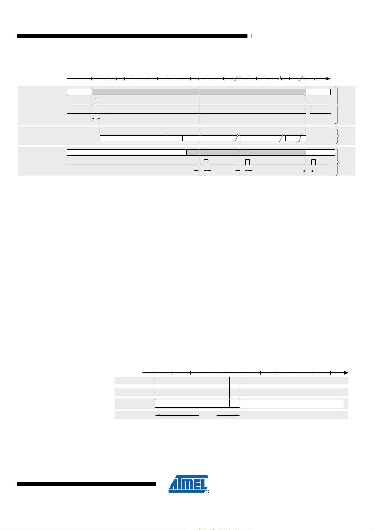
ATmega128RFA1
Figure 9-13. Timing of TRX24_RX_START, TRX24_XAH_AMI, TRX24_TX_END and TRX24_RX_END Interrupts in
Basic Operating Mode
1 2 8 1 6 0 1 9 20 1 9 2 + ( 9 + m ) *3 2- 1 6 T im e [ µ s ]
T R X _ S T A T E
S L P T R
I R Q
T y p . P r o c e s si n g D e l ay
P L L _ O N B U S Y _ T X P L L _ O N
1 6 µ s
F r a m e C o n t en t M H R
T R X _ S T A T E
I R Q
I n te r ru p t la te n c y
9.4.1.4 Basic Operating Mode Timing
The following paragraphs depict state transitions and their timing properties. Timing
figures are explained in Table 9-3 on page 42 and section "Digital Interface Timing
Characteristics" on page 507.
4 1 1 mN u m b e r o f O c t e ts
P r ea m b l e
R X _ O N R X _ O N
S F D P H R
9.4.1.4.1 Wake-up Procedure
The wake-up procedure from radio transceiver SLEEP state is shown in Figure 9-14
below. This figure implies, that the microcontroller is already running and hence, the
digital voltage regulator is enabled. If the microcontroller clock source is set to
Transceiver Clock, the crystal oscillator is also running, which reduces the radio
transceiver wake-up time further. For information about the wake-up timing of the
microcontroller, depending on the different clock source options, refer to "System Clock
and Clock Options" on page 147.
7
B U S Y _ R X
T R X 2 4 _ R X _ S T A R T
t
IR Q
M S D U
T R X 2 4 _ X A H _ A M I
t
IR Q
T R X 2 4 _ TX _ E N D
2
F C S
T R X 2 4 _
R X _ E N D
t
IR Q
TX
(Device1)
on Air
Frame
RX
(Device 2)
8266A-MCU Wireless-12/09
In order to calculate the total wake-up delay from microcontroller sleep mode (see
"Power Management and Sleep Modes" on page 156), the microcontroller wake-up
time, including the voltage regulator ramp-up and the radio transceiver wake-up time
has to be added.
Figure 9-14. Wake-up Procedure from Transceiver SLEEP State
0
Eve n t
State
Block
Tim e
The radio transceiver SLEEP state is left by releasing bit SLPTR to “0”. This restarts the
XOSC if it is not already running. After t
page 42) the radio transceiver enters TRX_OFF state. If the XOSC is already running,
the radio transceiver enters TRX_OFF state after 25 µs.
SL EEP
XO SC startup XOSC en ab le dFT N
10 0
20 0
TR X 24_ AW AKE I RQSL P TR = 0
TR X _OFF
t
TR 2
= 215 µs + 25 µs = 240 µs (see Table 9-3 on
TR2
40 0
Time [µs]
39
Page 40

ATmega128RFA1
During this wake-up procedure the calibration of the filter-tuning network (FTN) is
performed. Entering TRX_OFF state is signaled by the TRX24_AWAKE interrupt, if
enabled.
9.4.1.4.2 PLL_ON and RX_ON States
The transition from TRX_OFF to PLL_ON and RX_ON mode is shown in
below.
Figure 9-15
Figure 9-15. Transition from TRX_OFF to PLL_ON and RX_ON State
0
Event
State
Block
Command
Time
Note: 1. If TRX_CMD = RX_ON in TRX_OFF state RX_ON state is entered immediately,
Entering the commands PLL_ON or RX_ON in TRX_OFF state initiates a ramp-up
sequence of the internal 1.8V voltage regulator for the analog domain (AVREG), if
AVREG is not already enabled by the AVR ADC module. RX_ON state can be entered
any time from PLL_ON state regardless whether the PLL has already locked as
indicated by the TRX24_PLL_LOCK interrupt.
TRX_OFF
AVR EG
PLL_ON
even if the PLL has not settled.
2. If the AVR ADC module is enabled, the AVREG is already started and thus the
state transition time t
PLL
t
TR4
is reduced.
TR4
100 Time [µ s]
TRX24_PLL _LO CK IRQ
PLL_ON
RX_ON
RX
RX_ON
t
TR8
9.4.1.4.3 BUSY_TX and RX_ON States
The transition from PLL_ON to BUSY_TX state and subsequent to RX_ON state is
shown in Figure 9-16 below.
Figure 9-16. PLL_ON to BUSY_TX to RX_ON Timing
Even t
Sta te
Blo ck
Comm a nd
Tim e
Starting from PLL_ON state it is assumed that the PLL is already locked. A
transmission is initiated either by writing “1” to bit SLPTR or by command TX_START.
The PLL settles to the transmit frequency and the PA is enabled.
40
SL P TR
PL L_O N RX _ONBU SY_ T X
PA PL LPA , TX RXPL L
or com m and TX_ STA R T
t
TR 10
RX_ O N
Tim e [µ s]0 x16 x + 32
t
TR 11
8266A-MCU Wireless-12/09
Page 41

ATmega128RFA1
9.4.1.4.4 Reset Procedure
t
= 16 µs after initiating the transmission, the radio transceiver changes into
TR10
BUSY_TX state and the internally generated SHR is transmitted. After that the PSDU
data are transmitted from the Frame Buffer.
After completing the frame transmission, indicated by the TRX24_TX_END interrupt,
the PLL settles back to the receive frequency within t
If during TX_BUSY the radio transmitter is programmed to change to a receive state it
automatically proceeds the state change to RX_ON state after finishing the
transmission.
The radio transceiver reset procedure is shown in Figure 9-17 below.
= 32 µs in state PLL_ON.
TR11
3x AV R cl ock
x
x + 1 0
F T N
x + 4 0
[T RX 2 4_ AW A KE I R Q]
T R X_ O F F
> t1 1
t
TR 1 3
= 37 µs refers to Table 9-3 on page 42; t11 refers to "Digital
TR13
T im e [µ s]
Figure 9-17. Reset Procedure
0
E v en t
S t a te
B l o ck
T R X R ST
T im e
Note: 1. Timing parameter t
TRXRST = “1” resets all radio transceiver registers to their default values.
The radio transceiver reset is released automatically after 3 AVR clock cycles and the
wake-up sequence without restarting XOSC and DVREG, nevertheless an FTN
calibration cycle is performed, refer to "Automatic Filter Tuning (FTN)" on page 83. After
that the TRX_OFF state is entered.
Figure 9-17 above illustrates the radio transceiver reset procedure if the radio
transceiver is in any state but not in SLEEP state.
If the radio transceiver was in SLEEP state, the SLPTR bit in the TRXPR register must
be cleared prior to clearing the TRXRST bit in order to enter the TRX_OFF state.
Otherwise the radio transceiver enters the SLEEP state immediately.
v a ri o us
X O S C, D V R EG e na bl e d X O SC , DV R E G e na ble d
Interface Timing Characteristics" on page 507.
2. If TRXRST is set during radio transceiver SLEEP state, the XOSC startup delay is
extended by the XOSC startup time.
8266A-MCU Wireless-12/09
If the radio transceiver was in SLEEP state and the Transceiver Clock is not selected as
the microcontroller clock source, the XOSC is enabled before entering TRX_OFF state.
If register TRX_STATUS indicates STATE_TRANSITION_IN_PROGRESS during
system initialization until the radio transceiver reaches TRX_OFF, do not try to initiate a
further state change while the radio transceiver is in this state.
Note that before accessing the radio transceiver module the TRX24_AWAKE event
should be checked.
41
Page 42

ATmega128RFA1
9.4.1.4.5 State Transition Timing Summary
The transition numbers correspond to
"Basic Application Schematic" on page 493.
Table 9-3. Radio Transceiver State Transition Timing
No Symbol
1 t
2 t
3 t
4 t
5 t
6 t
7 t
8 t
9 t
10 t
11 t
12 t
13 t
SLEEP TRX_OFF 240
TR2
TRX_OFF SLEEP 35 · 1 / f
TR3
TRX_OFF PLL_ON 110 Depends on external capacitor at AVDD (1 µF nom)
TR4
PLL_ON TRX_OFF 1
TR5
TRX_OFF RX_ON 110 Depends on external capacitor at AVDD (1 µF nom)
TR6
RX_ON TRX_OFF 1
TR7
PLL_ON RX_ON 1
TR8
RX_ON PLL_ON 1 Transition time is also valid for TX_ARET_ON, RX_AACK_ON
TR9
TR10
TR11
TR12
TR13
TR14
PLL_ON BUSY_TX 16
BUSY_TX PLL_ON 32 PLL settling time from TX_BUSY to PLL_ON state
All modes TRX_OFF 1
RESET TRX_OFF 37 Not valid for SLEEP state
Various
states
Transition Time [µs], (typ) Comments
PLL_ON 1
CLKM
Table 9-3 below. See measurement setup in
Depends on crystal oscillator setup (CL = 10 pf)
TRX_OFF state indicated by TRX24_AWAKE interrupt
For f
> 250 kHz
CLKM
When setting bit SLPTR or TRX_CMD = TX_START, the first
symbol transmission is delayed by 16 µs (PLL settling and
PA ramp up).
Using TRX_CMD = FORCE_TRX_OFF (see register
TRX_STATE),
Not valid for SLEEP state
Using TRX_CMD = FORCE_PLL_ON (see register
TRX_STATE),
Not valid for SLEEP, RESET and TRX_OFF
The state transition timing is calculated based on the timing of the individual blocks
shown in Table 9-8 on page 51. The worst case values include maximum operating
temperature, minimum supply voltage, and device parameter variations.
Table 9-8. Analog Block Initialization and Settling Time
No Symbol Block Time [µs], (typ) Time [µs], (max) Comments
15 t
16 t
17 t
18 t
19 t
20 t
21 t
22 t
23 t
XOSC 215 1000
TR15
FTN 25 FTN tuning time, fixed
TR16
DVREG 60 1000
TR17
AVREG 60 1000
TR18
PLL, initial 110 155
TR19
PLL, settling 11 24 Settling time between channel switch
TR20
PLL, CF cal 35
TR21
PLL, DCU cal 6
TR22
PLL, RX TX
TR23
16 Maximum PLL settling time RX TX
Leaving SLEEP state, depends on crystal Q factor and load
capacitor
Depends on external bypass capacitor at DVDD
(CB3 = 1 µF nom., 10 µF worst case), depends on V
Depends on external bypass capacitor at AVDD
(CB1 = 1 µF nom., 10 µF worst case) , depends on V
PLL settling time TRX_OFF PLL_ON, including 60 µs
AVREG settling time
PLL center frequency calibration, refer to "Calibration
Loops" on page 83
PLL DCU calibration, refer to "Calibration Loops" on
page 83
DEVDD
EVDD
42
8266A-MCU Wireless-12/09
Page 43

ATmega128RFA1
No Symbol Block Time [µs], (typ) Time [µs], (max) Comments
24 t
25 t
PLL, TX RX
TR24
RSSI, update 2
TR25
32 Maximum PLL settling time TX RX
RSSI update period in receive states, refer to "Reading
RSSI" on page 68
26 t
27 t
28 t
29 t
9.4.2 Extended Operating Mode
ED 140
TR26
SHR, sync 96
TR27
CCA 140
TR28
Random value
TR29
ED measurement period, refer to "Measurement
Description" on page 69
Typical SHR synchronization period, refer to
"Measurement Description" on page 69
CCA measurement period, refer to "Configuration and
CCA Request" on page 71
1
The Extended Operating Mode is a hardware MAC accelerator and goes beyond the
basic radio transceiver functionality provided by the Basic Operating Mode. It handles
time critical MAC tasks requested by the IEEE 802.15.4 standard or by hardware such
as automatic acknowledgement, automatic CSMA-CA and retransmission. This results
in a more efficient IEEE 802.15.4 software MAC implementation including reduced code
size and may allow operating at lower microcontroller clock rates.
The Extended Operating Mode is designed to support IEEE 802.15.4-2006 compliant
frames; the mode is backward compatible to IEEE 802.15.4-2003 and supports non
IEEE 802.15.4 compliant frames. This mode comprises the following procedures:
Automatic acknowledgement (RX_AACK) divides into the tasks:
Random value update period, refer to "Random
Number Generator" on page 85
• Frame reception and automatic FCS check;
• Configurable addressing fields check;
• Interrupt indicating address match;
• Interrupt indicating frame reception, if it passes address filtering and FCS check;
• Automatic ACK frame transmission (if the received frame passed the address filter
and FCS check and if an ACK is required by the frame type and ACK request);
• Support of slotted acknowledgment using SLPTR bit for frame start.
Automatic CSMA-CA and Retransmission (TX_ARET) divides into the tasks:
• CSMA-CA including automatic CCA retry and random back-off;
• Frame transmission and automatic FCS field generation;
• Reception of ACK frame (if an ACK was requested);
• Automatic frame retry if ACK was expected but not received;
• Interrupt signaling with transaction status.
Automatic FCS check and generation (refer to "Frame Check Sequence (FCS)" on
page 66) is used by the RX_AACK and TX_ARET modes. In RX_AACK mode an
automatic FCS check is always performed for incoming frames.
An ACK received in TX_ARET mode within the time required by IEEE 802.15.4 is
accepted if the FCS is valid and if the sequence number of the ACK matches the
sequence number of the previously transmitted frame. Dependent on the value of the
8266A-MCU Wireless-12/09
43
Page 44

ATmega128RFA1
frame pending subfield in the received acknowledgement frame the transaction status is
set according to
Table 9-16 on page 58.
The state diagram including the Extended Operating Mode states is shown in Figure 9-
18 below. Yellow marked states represent the Basic Operating Mode; blue marked
states represent the Extended Operating Mode.
Figure 9-18. Extended Operating Mode State Diagram
2
SL E EP
(S lee p S tate)
X OS C= OF F
0
=
R
T
P
L
S
P
L
S
3
1
=
R
T
(fr o m a ll s ta te s)
TR XR ST = 1
N
T
TR X _O F F
(C loc k S ta te)
XO SC =O N
F
F
O
_
X
R
8
R X _O N
PL L_ O N
57
T
P
L
R
X
_
O
F
F
9
B U S Y _ R X
(R ec ei v e S ta te)
FO RC E_ TR X _O FF
(a ll m od es ex c ept S L E E P )
6
S H R
D et e cte d
Fr am e
E nd
R X _ O N
(R x L is ten S tat e )
O
_
X
R
N
N
O
O
_
_
L
K
L
C
P
Fr om / To
TR X_ OFF
N
O
_
F
K
F
C
O
A
_
A
X
_
R
X
T
R
S H R
D et ect e d
B U S Y _ R X _A A C K B U S Y _ T X _ A RE T
Tr ans ac tio n
F in is hed
A
_
X
R
A
TX _ A R E T_O NR X _A A CK _ O N
TR XR ST = 012 13
L
_
O
N
4
PL L _ O N
(P LL S ta te)
PLL_ON
R E S E T
SL PT R = 1
or
TX _S TA R T
11
10
Fr am e
E nd
14
FO RC E_ P L L _O N
se e no tes
Fr om / To
A
_
X
T
TR X_ OFF
N
O
_
T
E
R
_
X
R
T
S LP TR = 1
TX _S TA R T
F
F
O
or
Fr am e
E nd
TX_ARET_ON
B U SY _ T X
(T ran sm it S tat e )
44
Le ge nd:
B lu e : R egi st e r W ri te to T R X _ STAT E
R ed : Con trol s ign als v ia Re gis te r TRXPR
G re en: E ve nt
B as ic O pe ra ti ng M od e S tat es
E xte nde d O pe ra ti ng M o de S ta te s
Note: 1. State transition numbers correspond to Table 9-3 on page 42.
8266A-MCU Wireless-12/09
Page 45

ATmega128RFA1
9.4.2.1 State Control
The Extended Operating Mode states RX_AACK and TX_ARET are controlled via the
bits TRX_CMD of register TRX_STATE, which receives the state transition commands.
The states are entered from TRX_OFF or PLL_ON state as illustrated in Figure 9-18 on
page 44. The completion of each state change command shall always be confirmed by
reading the TRX_STATUS register.
RX_AACK - Receive with Automatic ACK
A state transition to RX_AACK_ON from PLL_ON or TRX_OFF is initiated by writing the
command RX_AACK_ON to the register bits TRX_CMD. The state change can be
confirmed by reading register TRX_STATUS, those changes to RX_AACK_ON or
BUSY_RX_AACK on success. BUSY_RX_AACK is returned if a frame is currently
being received.
The RX_AACK state is left by writing command TRX_OFF or PLL_ON to the register
bits TRX_CMD. If the radio transceiver is within a frame receive or acknowledgment
procedure (BUSY_RX_AACK) the state change is executed after finish. Alternatively,
the commands FORCE_TRX_OFF or FORCE_PLL_ON can be used to cancel the
RX_AACK transaction and change into radio transceiver state TRX_OFF or PLL_ON
respectively.
TX_ARET - Transmit with Automatic Retry and CSMA-CA Retry
Similarly, a state transition to TX_ARET_ON from PLL_ON or TRX_OFF is initiated by
writing command TX_ARET_ON to register bits TRX_CMD. The radio transceiver is in
the TX_ARET_ON state after TRX_STATUS register changes to TX_ARET_ON. The
TX_ARET transaction is started with writing ‘1’ to the SLPTR bit of the TRXPR register
or writing the command TX_START to register bits TRX_CMD.
TX_ARET state is left by writing the command TRX_OFF or PLL_ON to the register bits
TRX_CMD. If the radio transceiver is within a CSMA-CA, a frame-transmit or an
acknowledgment procedure (BUSY_TX_ARET) the state change is executed after
finish. Alternatively, the command FORCE_TRX_OFF or FORCE_PLL_ON can be
used to instantly terminate the TX_ARET transaction and change into radio transceiver
states TRX_OFF or PLL_ON, respectively.
Note that a state change request from TRX_OFF to RX_AACK_ON or TX_ARET_ON
internally passes the state PLL_ON to initiate the radio transceiver. Thus the readiness
to receive or transmit data is delayed accordingly. It is recommended to use interrupt
TRX24_PLL_LOCK as an indicator.
9.4.2.2 Configuration
8266A-MCU Wireless-12/09
The use of the Extended Operating Mode is based on Basic Operating Mode
functionality. Only features beyond the basic radio transceiver functionality are
described in the following sections. For details on the Basic Operating Mode refer to
section "Basic Operating Mode" on page 35.
When using the RX_AACK or TX_ARET modes, the following registers needs to be
configured.
RX_AACK configuration steps:
• Short address, PAN-ID and IEEE address (register SHORT_AADR_0,
SHORT_ADDR_1, PAN_ID_0, PAN_ID_1, IEEE_ADDR_0 … IEEE_ADDR_7)
• Configure RX_AACK properties (register XAH_CTRL_0, CSMA_SEED_1)
o Handling of Frame Version Subfield
45
Page 46

ATmega128RFA1
o Handling of Pending Data Indicator
o Characterize as PAN coordinator
o Handling of Slotted Acknowledgement
• Additional Frame Filtering Properties (register XAH_CTRL_1, CSMA_SEED_1)
o Promiscuous Mode
o Enable or disable automatic ACK generation
o Handling of reserved frame types
The addresses for the address match algorithm are to be stored in the appropriate
address registers. Additional control of the RX_AACK mode is done with registers
XAH_CTRL_1 and CSMA_SEED_1.
As long as a short address has not been set, only broadcast frames and frames
matching the IEEE address can be received.
Configuration examples for different device operating modes and handling of various
frame types can be found in section
page 49.
TX_ARET configuration steps:
• Leave register bit TX_AUTO_CRC_ON = 1 register TRX_CTRL_1
• Configure CSMA-CA
o MAX_FRAME_RETRIES register XAH_CTRL_0
o MAX_CSMA_RETRIES register XAH_CTRL_0
o CSMA_SEED registersCSMA_SEED_0, CSMA_SEED_1
o MAX_BE, MIN_BE register CSMA_BE
• Configure CCA (see section "Configuration and CCA Request" on page 71)
MAX_FRAME_RETRIES (register XAH_CTRL_0) defines the maximum number of
frame retransmissions.
"Description of RX_AACK Configuration Bits" on
The register bits MAX_CSMA_RETRIES (register XAH_CTRL_0) configure the number
of CSMA-CA retries after a busy channel is detected.
The CSMA_SEED_0 and CSMA_SEED_1 registers define a random seed for the backoff-time random-number generator of the radio transceiver.
The MAX_BE and MIN_BE register bits (register CSMA_BE) set the maximum and
minimum CSMA back-off exponent (according to [1] on page 100).
9.4.2.3 RX_AACK_ON – Receive with Automatic ACK
The general functionality of the RX_AACK procedure is shown in Figure 9-19 on page
48.
The gray shaded area is the standard flow of a RX_AACK transaction for
IEEE 802.15.4 compliant frames (refer to section "Configuration of IEEE Scenarios" on
page 50). All other procedures are exceptions for specific operating modes or frame
formats (refer to section "Configuration of non IEEE 802.15.4 Compliant Scenarios" on
page 52).
The frame filtering operation is described in detail in section "Frame Filtering" on page
54.
In RX_AACK_ON state, the radio transceiver listens for incoming frames. After
detecting SHR and a valid PHR, the radio transceiver parses the frame content of the
MAC header (MHR) as described in section "PHY Header (PHR)" on page 61.
46
8266A-MCU Wireless-12/09
Page 47

ATmega128RFA1
Generally, at nodes, configured as a normal device or PAN coordinator, a frame is not
indicated if the frame filter does not match and the FCS is invalid. Otherwise, the
TRX_24_RX_END interrupt is issued after the completion of the frame reception. The
microcontroller can then read the frame. An exception applies if promiscuous mode is
enabled (see section "Configuration of IEEE Scenarios" on page 50). In that case a
TRX_24_RX_END interrupt is issued even if the FCS fails.
If the content of the MAC addressing fields of the received frame (refer to
IEEE 802.15.4 section 7.2.1) matches one of the configured addresses, dependent on
the addressing mode, an address match interrupt (TRX24_XAH_AMI) is issued (refer to
section "Frame Filtering" on page 54). The expected address values are to be stored in
registers Short-address, PAN-ID and IEEE-address. Frame filtering as described in
section "Frame Filtering" on page 54 is also valid for Basic Operating Mode.
During reception the radio transceiver parses bit[5] (ACK Request) of the frame control
field of the received data or the MAC command frame to check if an ACK reply is
expected. In that case and if the frame passes the third level of filtering (see
IEEE 802.15.4-2006, section 7.5.6.2), the radio transceiver automatically generates and
transmits an ACK frame. After the ACK transmission is finished, a TRX24_TX_END
interrupt is generated.
The content of the frame pending subfield of the ACK response is set by bit
AACK_SET_PD of register CSMA_SEED_1 when the ACK frame is sent in response to
a data request MAC command frame, otherwise this subfield is set to “0”. The
sequence number is copied from the received frame.
Optionally, the start of the transmission of the acknowledgement frame can be
influenced by register bit AACK_ACK_TIME. Default value (according to standard
IEEE 802.15.4, page 54) is 12 symbol times after the reception of the last symbol of a
data or MAC command frame.
If the bit AACK_DIS_ACK of register CSMA_SEED_1 is set, no acknowledgement
frame is sent even if an acknowledgment frame was requested. This is useful for
operating the MAC hardware accelerator in promiscuous mode (see section
"Configuration of non IEEE 802.15.4 Compliant Scenarios" on page 52).
The status of the RX_AACK operation is indicated by the bits TRAC_STATUS of
register TRAC_STATUS.
During the operations described above the radio transceiver remains in
BUSY_RX_AACK state.
8266A-MCU Wireless-12/09
47
Page 48
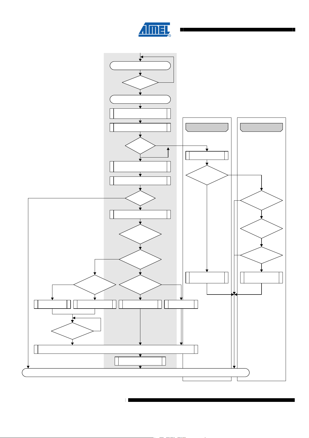
ATmega128RFA1
Figure 9-19. Flow Diagram of RX_AACK
TRX _S TAT E = RX _AA CK _O N
Note 1: Fra me Filterin g, Pr om iscu ous Mode and
Rese rved Frame s:
- A rad io tra nsceiv er in P rom iscu ous
Mode , or con figu red to rece ive Res erv ed
Fram es h andles rec eived f ram es p assing
the th ird leve l of filte ring
- Fo r detai ls re fer to th e desc ripti on of
Prom iscu ous M ode and Re served
Fram e T ypes
Note 2: FCS check is omi tted for Pro mis cou s M ode
Note 3: Add itional con diti ons:
- AC K requ este d &
- AC K_DIS _ACK= =0 &
- fra me_ve rsion<= AACK_ FVN _MOD E
N
AAC K_ ACK_T IME
== 0
Y
Wait 2 symbol
peri ods
Wa it 6 sym bol
periods
SHR de tected
TRX _S TAT E = BU SY _RX _A ACK
Gen era te TRX24_ RX_ST ART
interrup t
Scannin g M HR
N
Y
Fra me
Filte ring
Y
Gen era te T RX24_ XAH _AMI
interrup t
Fra me receptio n
N
(see Note 1 )
N
FCS valid
(see Note 2 )
Gen era te T RX24_ RX_EN D
N
N
AAC K_ ACK _T IME
Y
interrup t
ACK re quested
(see Note 3 )
Y
Slot ted Ope ration
== 0
Y
== 0
Y
Wait 12 sym bol
per iods
N
Wa it 2 symbol
AAC K_ PROM_MODE
periods
Pro miscuou s M ode
Fra me receptio n
== 1
Y
Gen era te
TRX 24_RX _END
interrup t
Res erved F ram es
N
N
N
N
FCF [2:0]
> 3
Y
AACK_UPLD_R ES_FT
== 1
Y
FCS va lid
Y
Gen era te
TRX 24_RX _END
interrup t
SLP TR bit
= 1
48
N
Y
Tra nsm it A CK
Gen erateTRX2 4_T X_END
interrup t
TRX _S TAT E = RX _AA CK _O N
8266A-MCU Wireless-12/09
Page 49

ATmega128RFA1
9.4.2.3.1 Description of RX_AACK Configuration Bits
Overview
The following table summarizes all register bits which affect the behavior of a
RX_AACK transaction. For address filtering it is further required to setup address
registers to match to the expected address.
Configuration and address bits are to be set in TRX_OFF or PLL_ON state prior to
switching to RX_AACK mode.
A graphical representation of various operating modes is illustrated in Figure 9-19 on
page 48.
Table 9-5. Overview of RX_AACK Configuration Bits
Register Name Register Bits Description
SHORT_ADDR_0/1
PAN_ADDR_0/1
IEEE_ADDR_0
…
IEEE_ADDR_7
RX_SAFE_MODE 7 Protect buffer after frame receive
AACK_PROM_MODE 1 Support promiscuous mode
AACK_ACK_TIME 2 Change auto acknowledge start time
AACK_UPLD_RES_FT 4 Enable reserved frame type reception, needed to
AACK_FLTR_RES_FT 5 Filter reserved frame types like data frame type,
SLOTTED_OPERATION 0 If set, acknowledgment transmission has to be
AACK_I_AM_COORD 3 If set, the device is a PAN coordinator
AACK_DIS_ACK 4 Disable generation of acknowledgment
AACK_SET_PD 5 Set frame pending subfield in Frame Control Field
AACK_FVN_MODE 7:6 Controls the ACK behavior, depending on FCF
Set node addresses
receive non-standard compliant frames
needed for filtering of non-standard compliant
frames
triggered by register bit SLPTR
(FCF), refer to section "Overview" on page 66
frame version number
8266A-MCU Wireless-12/09
The usage of the RX_AACK configuration bits for various operating modes of a node is
explained in the following sections. Configuration bits not mentioned in the following two
sections should be set to their reset values.
All registers mentioned in Table 9-5 above are described in section "Register Summary"
on page 60.
Note, that the general behavior of the Extended Feature Set settings:
• OQPSK_DATA_RATE (PSDU data rate)
• SFD_VALUE (alternative SFD value)
• ANT_DIV (Antenna Diversity)
• RX_PDT_LEVEL (blocking frame reception of lower power signals)
are completely independent from RX_AACK mode (see "Radio Transceiver Extended
Feature Set" on page 85). Each of these operating modes can be combined with the
RX_AACK mode.
49
Page 50

ATmega128RFA1
9.4.2.3.2 Configuration of IEEE Scenarios
Normal Device
The
Table 9-6 below shows a typical RX_AACK configuration of an IEEE 802.15.4
device operated as a normal device rather than a PAN coordinator or router.
Table 9-6. Configuration of IEEE 802.15.4 Devices
Register Name Register Bits Description
SHORT_ADDR_0/1
PAN_ADDR_0/1
IEEE_ADDR_0
IEEE_ADDR_7
RX_SAFE_MODE 7 0: disable frame protection
SLOTTED_OPERATION 0 0: if transceiver works in unslotted mode
AACK_FVN_MODE 7:6 Controls the ACK behavior, depending on FCF
Notes: 1. If no short address has been configured before the device has been assigned one
Set node addresses
…
by the PAN-coordinator, only frames directed to either the broadcast address or
the IEEE address are received.
2. In IEEE 802.15.4-2003 standard the frame version subfield did not yet exist but
was marked as reserved. According to this standard, reserved fields have to be set
to zero. On the other hand, IEEE 802.15.4-2003 standard requires ignoring
reserved bits upon reception. Thus, there is a contradiction in the standard which
can be interpreted in two ways:
a) If a network should only allow access to nodes which use the
IEEE 802.15.4-2003, then AACK_FVN_MODE should be set to 0.
b) If a device should acknowledge all frames independent of its frame version,
AACK_FVN_MODE should be set to 3. However, this can result in conflicts with
co-existing IEEE 802.15.4-2006 standard compliant networks.
The same holds for PAN coordinators as described below.
1: enable frame protection
1: if transceiver works in slotted mode
frame version number
0x00 : acknowledges only frames with version
number 0, i.e. according to IEEE 802.15.4-2003
frames
0x01 : acknowledges only frames with version
number 0 or 1, i.e. frames according to
IEEE 802.15.4-2006
0x10 : acknowledges only frames with version
number 0 or 1 or 2
0x11 : acknowledges all frames, independent of
the FCF frame version number
50
PAN-Coordinator
Table 9-7 on page 51 shows the RX_AACK configuration for a PAN coordinator.
8266A-MCU Wireless-12/09
Page 51

ATmega128RFA1
Table 9-7. Configuration of a PAN Coordinator
Register Name Register Bits Description
SHORT_ADDR_0/1
PAN_ADDR_0/1
IEEE_ADDR_0
…
IEEE_ADDR_7
RX_SAFE_MODE 7 0: disable frame protection
SLOTTED_OPERATION 0 0: if transceiver works in unslotted mode
AACK_I_AM_COORD 3 1: device is PAN coordinator
AACK_SET_PD 5 0: frame pending subfield is not set in FCF
AACK_FVN_MODE 7:6 Controls the ACK behavior, depends on FCF
Set node addresses
1: enable frame protection
1: if transceiver works in slotted mode
1: frame pending subfield is set in FCF
frame version number
0x00 : acknowledges only frames with version
number 0, i.e. according to IEEE 802.15.4-2003
frames
0x01 : acknowledges only frames with version
number 0 or 1, i.e. frames according to
IEEE 802.15.4-2006
0x10 : acknowledges only frames with version
number 0 or 1 or 2
0x11 : acknowledges all frames, independent of
the FCF frame version number
Promiscuous Mode
The promiscuous mode is described in IEEE 802.15.4-2006, section 7.5.6.5. This mode
is further illustrated in Radio Transceiver Extended Feature Set on page 85. According
to IEEE 802.15.4-2006 when in promiscuous mode, the MAC sub layer shall pass
received frames with correct FCS to the next higher layer without further processing.
That implies that frames should never be acknowledged.
Only second level filter rules as defined by IEEE 802.15.4-2006, section 7.5.6.2, are
applied to the received frame.
Table 9-8 below shows the typical configuration of a device operating in promiscuous
mode.
Table 9-8. Configuration of Promiscuous Mode
Register Name Register Bits Description
SHORT_ADDR_0/1
PAN_ADDR_0/1
IEEE_ADDR_0
…
IEEE_ADDR_7
AACK_PROM_MODE 1 1: Enable promiscuous mode
AACK_DIS_ACK 4 1: Disable generation of acknowledgment
Each address shall be set: 0x00
8266A-MCU Wireless-12/09
51
Page 52

ATmega128RFA1
Register Name Register Bits Description
AACK_FVN_MODE 7:6 Controls the ACK behavior, depends on FCF frame
version number
0x00 : acknowledges only frames with version
number 0, i.e. according to IEEE 802.15.4-2003
frames
0x01 : acknowledges only frames with version
number 0 or 1, i.e. frames according to
IEEE 802.15.4-2006
0x10 : acknowledges only frames with version
number 0 or 1 or 2
0x11 : acknowledges all frames, independent of the
FCF frame version number
Second level of filtering according to IEEE 802.15.4-2006, section 7.5.6.2, is applied to
a received frame if the radio transceiver is in promiscuous mode. However, a
TRX24_RX_END interrupt is issued even if the FCS is invalid. Thus it is necessary to
read bit RX_CRC_VALID of register PHY_RSSI after the TRX24_RX_END interrupt in
order to verify the reception of a frame with a valid FCS.
If a device, operating in promiscuous mode, receives a frame with a valid FCS which in
addition passed the third level filtering according to IEEE 802.15.4-2006, section
7.5.6.2, an acknowledgement frame would be transmitted. According to the definition of
the promiscuous mode a received frame shall not be acknowledged even if it is
requested. Thus bit AACK_DIS_ACK of register CSMA_SEED_1 has to be set to 1.
In all receive modes a TRX24_AMI interrupt is issued, when the received frame
matches the node’s address according to the filter rules described in section "Frame
Filtering" on page 54.
Alternatively, in RX_ON state of the Basic Operating Mode when a valid PHR is
detected a TRX24_RX_START interrupt is generated and the frame is received. The
end of the frame reception is signalized with a TRX24_RX_END interrupt. At the same
time the bit RX_CRC_VALID of register PHY_RSSI is updated with the result of the
FCS check (see "Overview" on page 66). The RX_CRC_VALID bit must be checked in
order to dismiss corrupted frames according to the definition of the promiscuous mode.
9.4.2.3.3 Configuration of non IEEE 802.15.4 Compliant Scenarios
Sniffer
52
Table 9-9 below shows a RX_AACK configuration to setup a sniffer device. Other
RX_AACK configuration bits should be set to their reset values (see Table 9-5 on page
49). All frames received are indicated by a TRX24_RX_START and TRX24_RX_END
interrupt. Bit RX_CRC_VALID of register PHY_RSSI is updated after frame reception
with the result of the FCS check (see "Overview" on page 66). The RX_CRC_VALID bit
needs to be checked in order to dismiss corrupted frames.
Table 9-9. Configuration of a Sniffer Device
Register Name Register Bits Description
AACK_PROM_MODE 1 1: Enable promiscuous mode
AACK_DIS_ACK 4 1: Disable generation of acknowledgment
This operating mode is similar to the promiscuous mode.
8266A-MCU Wireless-12/09
Page 53

ATmega128RFA1
Reception of Reserved Frames
Frames with reserved frame types (see section Table 9-16 on page 63) can also be
handled in RX_AACK mode. This might be required when implementing proprietary,
non-standard compliant protocols. It is an extension of the address filtering in
RX_AACK mode. Received frames are either handled similar to data frames or may be
allowed to completely bypass the address filter.
Table 9-10 below shows the required configuration for a node to receive reserved
frames and Figure 9-19 on page 48 shows the corresponding flow chart.
Table 9-10. RX_AACK Configuration to Receive Reserved Frame Types
Register Name Register Bits Description
SHORT_ADDR_0/1
PAN_ADDR_0/1
IEEE_ADDR_0
…
IEEE_ADDR_7
RX_SAFE_MODE 7 0: disable frame protection
AACK_UPLD_RES_FT 4 1 : Enable reserved frame type reception
AACK_FLTR_RES_FT 5 Filter reserved frame types like data frame type,
SLOTTED_OPERATION 0 0: if transceiver works in un-slotted mode
AACK_I_AM_COORD 3 0: device is not PAN coordinator
AACK_DIS_ACK 4 0: Enable generation of acknowledgment
AACK_FVN_MODE 7:6 Controls the ACK behavior, depends on FCF
Set node addresses
1: enable frame protection
see note below
0 : disable
1 : enable
1: if transceiver works in slotted mode
1: device is PAN coordinator
1: Disable generation of acknowledgment
frame version number
0x00 : acknowledges only frames with version
number 0, i.e. according to IEEE 802.15.4-2003
frames
0x01 : acknowledges only frames with version
number 0 or 1, i.e. frames according to
IEEE 802.15.4-2006
0x10 : acknowledges only frames with version
number 0 or 1 or 2
0x11 : acknowledges all frames, independent of
the FCF frame version number
8266A-MCU Wireless-12/09
There are two different options for handling reserved frame types.
1. AACK_UPLD_RES_FT = 1, AACK_FLT_RES_FT = 0:
Any non-corrupted frame with a reserved frame type is indicated by a
TRX24_RX_END interrupt. No further address filtering is applied on those frames.
A TRX24_AMI interrupt is never generated and the acknowledgment subfield is
ignored.
2. AACK_UPLD_RES_FT = 1, AACK_FLT_RES_FT = 1:
53
Page 54

ATmega128RFA1
If AACK_FLT_RES_FT = 1 any frame with a reserved frame type is filtered by the
address filter similar to a data frame as described in the standard. Consequently, a
TRX24_AMI interrupt is generated upon address match. A TRX24_RX_END
interrupt is only generated if the address matched and the frame was not
corrupted. An acknowledgment is only send, when the ACK request subfield was
set in the received frame and a TRX24_RX_END interrupt occurred.
Note that It is not allowed to set AACK_FLTR_RES_FT = 1 and have register bit
AACK_FLTR_RES_FT set to 0.
Short Acknowledgment Frame (ACK) Start Timing
The bit AACK_ACK_TIME of register XAH_CTRL_1 defines the symbol time between
frame reception and transmission of an acknowledgment frame.
9.4.2.4 Frame Filtering
Table 9-11. Overview of RX_AACK Configuration Bits
Register Name Register Bit Description
AACK_ACK_TIME 2 0: Standard compliant acknowledgement timing of 12
Note that this feature can be used in all scenarios, independent of other configurations.
However, shorter acknowledgment timing is especially useful when using High Data
Rate Modes to increase battery lifetime and to improve the overall data throughput; see
"High Data Rate Modes" on page 86 for details.
symbol periods. In slotted acknowledgement operation
mode, the acknowledgment frame transmission can be
triggered 6 symbol periods after reception of the frame
earliest.
1: Reduced acknowledgment timing of 2 symbol periods
(32 µs).
Frame Filtering is an evaluation whether or not a received frame is dedicated for this
node. To accept a received frame and to generate an address match interrupt
(TRX24_AMI) a filtering procedure as described in IEEE 802.15.4-2006 chapter 7.5.6.2.
(Third level of filtering) is applied to the frame. The radio transceiver’s RX_AACK mode
accepts only frames that satisfy all of the following requirements (quote from
IEEE 802.15.4-2006, 7.5.6.2):
1. The Frame Type subfield shall not contain a reserved frame type.
2. The Frame Version subfield shall not contain a reserved value.
3. If a destination PAN identifier is included in the frame, it shall match macPANId or
shall be the broadcast PAN identifier (0xFFFF).
4. If a short destination address is included in the frame, it shall match either
macShortAddress or the broadcast address (0xFFFF). Otherwise, if an extended
destination address is included in the frame, it shall match aExtendedAddress.
5. If the frame type indicates that the frame is a beacon frame, the source PAN
identifier shall match macPANId unless macPANId is equal to 0xFFFF, in which
case the beacon frame shall be accepted regardless of the source PAN identifier.
6. If only source addressing fields are included in a data or MAC command frame, the
frame shall be accepted only if the device is the PAN coordinator and the source
PAN identifier matches macPANId.
The radio transceiver requires two additional rules:
54
1. The frame type indicates that the frame is not an ACK frame (refer toTable 9-6 on
page 50).
8266A-MCU Wireless-12/09
Page 55

ATmega128RFA1
2. At least one address field must be configured.
Address match, indicated by the TRX24_AMI interrupt is further controlled by the
content of subfields of the frame control field of a received frame according to the
following rule:
If (Destination Addressing Mode = 0 OR 1) AND (Source Addressing Mode = 0) no
TRX24_AMI interrupt is generated, refer to Figure 9-26 on page 63. This effectively
causes all acknowledgement frames not to be announced which otherwise always pass
the filter regardless of whether they are intended for this device or not.
For backward compatibility to IEEE 802.15.4-2003 third level filter rule 2 (Frame
Version) can be disabled by the bits AACK_FVN_MODE of register CSMA_SEED_1.
Frame filtering is available in Extended and Basic Operating Mode (see section "Basic
Operating Mode" on page 35); a frame passing the frame filtering generates an
TRX24_AMI interrupt, if enabled.
Note: 1. Filter rule 1 is affected by register bits AACK_FLTR_RES_FT and
AACK_UPLD_RES_FT (see register "XAH_CTRL_1 – Transceiver
Acknowledgment Frame Control Register 1" on page 119).
2. Filter rule 2 is affected by register bits AACK_FVN_MODE (see register
"CSMA_SEED_1 – Transceiver Acknowledgment Frame Control Register 2" on
page 129).
9.4.2.4.1 RX_AACK Slotted Operation – Slotted Acknowledgement
The radio transceiver supports slotted acknowledgement operation according to
IEEE 802.15.4-2006, section 5.5.4.1.
In RX_AACK mode with bit SLOTTED_OPERATION of register XAH_CTRL_0 set, the
transmission of an acknowledgement frame has to be controlled by the microcontroller.
If an ACK frame has to be transmitted the radio transceiver expects writing SLPTR=1 to
actually start the transmission. This waiting state is signaled 6 symbol periods after the
reception of the last symbol of a data or MAC command frame by bits TRAC_STATUS
of register XAH_CTRL_0, which are set to SUCCESS_WAIT_FOR_ACK in that case. In
networks using slotted operation the start of the acknowledgment frame and thus the
exact timing must be provided by the microcontroller.
A timing example of an RX_AACK transaction with bit SLOTTED_OPERATION of
register XAH_CTRL_0 set is shown in the next figure. The acknowledgement frame is
ready to transmit 6 symbol times after the reception of the last symbol of a data or MAC
command frame. The transmission of the acknowledgement frame is initiated by the
microcontroller by writing SLPTR=1 and starts 16µs (t
t
is specified in section "Digital Interface Timing Characteristics" on page 507.
IRQ
) later. The interrupt latency
TR10
8266A-MCU Wireless-12/09
55
Page 56

ATmega128RFA1
Figure 9-10. Example Timing of an RX_AACK Transaction for Slotted Operation
64 102 6
51 20 704
tim e [µ s ]
Fr ame Ty pe
TR X_ STA TE
R X/ TX RX TX
IR Q
Ty p. P roc ess ing Del ay
SL PT R
9.4.2.4.2 RX_AACK Mode Timing
RX _A AC K_ ON
SF D
D ata Fra me (Len gth = 1 0, A CK =1) AC K F ram e
BU SY _R X_ AA CK
R X
wa itin g pe riod sig nale d b y re gist er b its T RA C _ST ATU S
If bit AACK_ACK_TIME of register XAH_CTRL_1 is set, an acknowledgment frame can
be sent already 2 symbol times after the reception of the last symbol of a data or MAC
command frame.
A timing example of an RX_AACK transaction is shown in the next figure. In this
example a data frame of length 10 with an ACK request is received. The radio
transceiver changes to state BUSY_RX_AACK after SFD detection. The completion of
the frame reception is indicated by a TRX24_RX_END interrupt. Interrupts
TRX24_RX_START and TRX24_AMI are disabled in this example. The ACK frame is
automatically transmitted after a default wait period of 12 symbols (192 µs), bit
AACK_ACK_TIME = 0 (reset value). The interrupt latency t
"Digital Interface Timing Characteristics" on page 507.
t
IRQ
TR X2 4_R X_E ND
96 µs
(6 sym bo ls)
t
AC K t rans mis sion ini tiate d b y m icro con troll er
SL PTR
TR 10
on Air
Frame
RX _A AC K_ ON
RX
TX
t
IRQ
is specified in section
IRQ
RX
TR X2 4_T X_E ND
RX/TX
Figure 9-11. Example Timing of an RX_AACK Transaction
51 20 704
Fr ame Ty pe
64 108 8
SF D
D ata Fra me (L eng th = 10 , A CK =1) AC K F ram e
TR X_ STA TE
RX /TX RX TX
IR Q
Ty p. P roc ess ing Dela y
RX _A ACK _O N BU SY _R X_A AC K
TR X24 _R X_E ND
t
IRQ
192 µ s
(12 sy mbo ls)
If bit AACK_ACK_TIME of register XAH_CTRL_1 is set, an acknowledgment frame is
sent already 2 symbol times after the reception of the last symbol of a data or MAC
command frame.
t
IRQ
tim e [ µ s]
RX _A ACK _O N
RX
TR X24 _T X_E ND
on Air
Frame
RX/TX
56
8266A-MCU Wireless-12/09
Page 57

ATmega128RFA1
9.4.2.5 TX_ARET_ON – Transmit with Automatic Retry and CSMA-CA Retry
Figure 9-12. Flow Diagram of TX_ARET
T R X _S T A T E = T X _A R ET _O N
fr a m e_ rc tr = 0
S ta rt TX
Y
T R X _S T A T E = B US Y_ TX _A RE T
T R A C_ S TA TU S = INV A L ID
(s ee No te 1 )
N
MA X_CS M A_RETRIES
<7
Y
cs ma_ rc tr = 0
R ando m B ac k -O ff
csm a _r ctr = cs ma _r ctr + 1
fr a m e_ rc tr = fr am e_ rc tr + 1
C C A
C CA
R esu lt
S u cce ss
T ra ns mi t F ra m e
A C K r eq u est e d
Y
N
F a ilu re
N
N ote 1: If M AX _C SM A _R E TR IE S = 7 no re try is
p er for me d
N
csm a_ rc tr >
MA X_ CS M A_ RE TR IES
Y
N
8266A-MCU Wireless-12/09
N
R ecei v e A CK
u ntil t im eo ut
A C K v ali d
fra m e_r ctr >
M AX _F RA M E _R ET RIE S
T R AC _S TA T U S =
N O_ AC K
Y
Y
N
D ata Pen din g
Y
T R A C_ S TA TU S =
S U C CE SS _D AT A_ PE ND IN G
Y
Is sue TR X2 4 _ T X _ EN D in ter ru pt
T R X _S T A TE = T X _ A R ET _O N
N
T R AC _S TA TU S =
S U CC ES S
T R AC _S TA T U S =
C H AN NE L_ AC CE SS _F AI LU R E
57
Page 58

ATmega128RFA1
Overview
The implemented TX_ARET algorithm is shown in
In TX_ARET mode, the radio transceiver first executes the CSMA-CA algorithm, as
defined by IEEE 802.15.4–2006, section 7.5.1.4, initiated by a transmit start event. If
the channel is IDLE a frame is transmitted from the Frame Buffer. If the
acknowledgement frame is requested the radio transceiver additionally checks for an
ACK reply.
A TRX24_TX_END interrupt indicates the completion of the TX_ARET transmit
transaction.
Description
Configuration and address bits are to be set in TRX_OFF or PLL_ON state prior to
switching to TX_ARET mode. It is further recommended to transfer the PSDU data to
the Frame Buffer in advance. The transaction is started by either writing SLPTR=1 as
described in section "Transceiver Pin Register TRXPR" on page 32 or writing a
TX_START command to register TRX_STATE.
If the CSMA-CA detects a busy channel, it is retried as specified by bits
MAX_CSMA_RETRIES of register XAH_CTRL_0. In case that CSMA-CA does not
detect a clear channel after MAX_CSMA_RETRIES it aborts the TX_ARET transaction,
issues a TRX24_TX_END interrupt and sets the value of the TRAC_STATUS register
bits to CHANNEL_ACCESS_FAILURE.
During transmission of a frame the radio transceiver parses bit 5 (ACK Request) of the
MAC header (MHR) frame control field of the PSDU data (PSDU octet #1) to be
transmitted to check if an ACK reply is expected.
Figure 9-12 on page 57.
If an ACK is expected the radio transceiver automatically switches into receive mode to
wait for a valid ACK reply. After receiving an ACK frame the Frame Pending subfield of
that frame is parsed and the status register bits TRAC_STATUS are updated
accordingly (see Table 9-16 below). This receive procedure does not overwrite the
Frame Buffer content. Transmit data in the Frame Buffer is not changed during the
entire TX_ARET transaction. Received frames other than the expected ACK frame are
discarded.
If no valid ACK is received or after timeout of 54 symbol periods (864 µs), the radio
transceiver retries the entire transaction (including CSMA-CA) until the maximum
number of retransmissions as set by the bits MAX_FRAME_RETRIES in register
XAH_CTRL_0 is exceeded.
After that, the microcontroller may read the value of the bits TRAC_STATUS of register
TRX_STATE to verify whether the transaction was successful or not. The register bits
are set according to the following cases:
Table 9-16. Interpretation of the TRAC_STATUS register bits
Value Name Description
0 SUCCESS The transaction was responded by a valid
ACK, or, if no ACK is requested, after a
successful frame transmission
1 SUCCESS_DATA_PENDING Equivalent to SUCCESS; indicates pending
3 CHANNEL_ACCESS_FAILURE Channel is still busy after
frame data according to the MHR frame
control field of the received ACK response
MAX_CSMA_RETRIES of CSMA-CA
58
8266A-MCU Wireless-12/09
Page 59
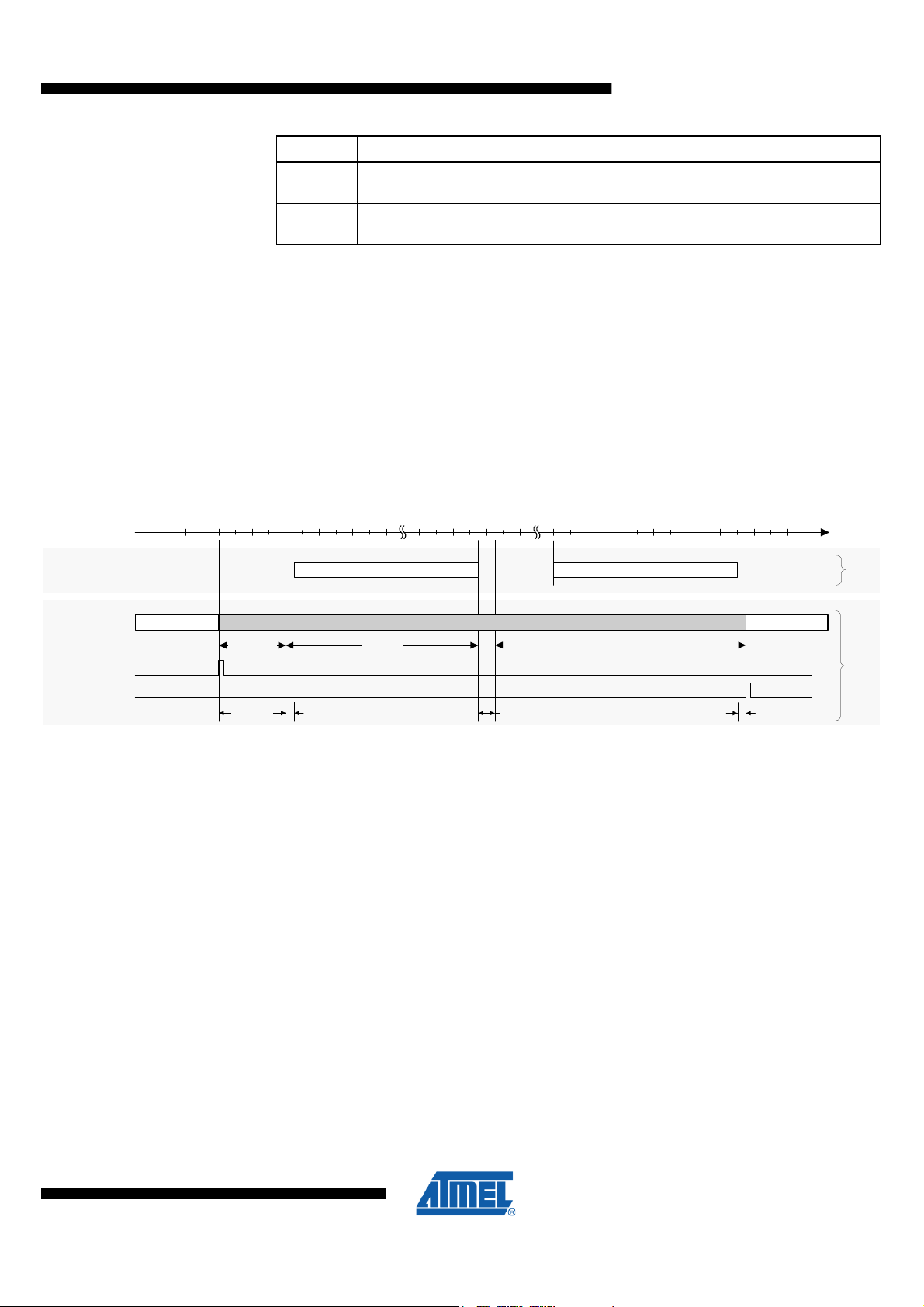
ATmega128RFA1
Value Name Description
5 NO_ACK No acknowledgement frames were received
7 INVALID Entering TX_ARET mode sets
Note that if no ACK is expected (according to the content of the received frame in the
Frame Buffer), the radio transceiver issues a TRX24_TX_END interrupt directly after
the frame transmission has been completed. The value of the bits TRAC_STATUS of
register TRX_STATE is set to SUCCESS.
A value of MAX_CSMA_RETRIES = 7 initiates an immediate TX_ARET transaction
without performing CSMA-CA. This is required to support slotted acknowledgement
operation. Further the value MAX_FRAME_RETRIES is ignored and the TX_ARET
transaction is performed only once.
A timing example of a TX_ARET transaction is shown in Figure 9-13 below .
Figure 9-13. Example Timing of a TX_ARET Transaction
12 8 x+35 2
67 20 x
during all retry attempts
TRAC_STATUS = 7
tim e [µ s]
Fra meTy pe
TR X_ ST ATE
RX /TX
SLP TR
IRQ
Typ . Proces sin g D elay
9.4.2.6 Interrupt Handling
TX_A RE T_ ON BU SY _TX_ AR ET
Data F rame (L eng th = 1 0, AC K=1) AC K F rame
TX
TXCSM A- CA
RX
RX
TX _A RE T_ ON
RX_ END
CSM A-C A
16 µs
Note: 1. t
Here an example data frame of length 10 with an ACK request is transmitted, see Table
9-13 on page 60. After the transmission the radio transceiver switches to receive mode
and expects an acknowledgement response. During the whole transaction including
frame transmit, wait for ACK and ACK receive the radio transceiver status register
TRX_STATUS signals BUSY_TX_ARET.
A successful reception of the acknowledgment frame is indicated by the
TRX24_TX_END interrupt. The status register TRX_STATUS changes back to
TX_ARET_ON. The TX_ARET status register TRAC_STATUS changes as well to
TRAC_STATUS = SUCCESS or TRAC_STATUS = SUCCESS_DATA_PENDING if the
frame pending subfield of the received ACK frame was set to 1.
defines the random CSMA-CA processing time.
CSMA-CA
32 µst
t
IRQ
on Air
Frame
RX/TX
8266A-MCU Wireless-12/09
The interrupt handling in the Extended Operating Mode is similar to the Basic Operating
Mode (see section "Interrupt Handling" on page 38). The microcontroller enables
interrupts by setting the appropriate bit in register IRQ_MASK.
For RX_AACK and TX_ARET the following interrupts (Table 9-13 on page 60) inform
about the status of a frame reception and transmission:
59
Page 60

ATmega128RFA1
Table 9-13. Interrupt Handling in Extended Operating Mode
Mode Interrupt Description
RX_AACK
TX_ARET TRX24_TX_END Signals completion of TX_ARET transaction
Both TRX24_PLL_LOCK Entering RX_AACK_ON or TX_ARET_ON state from
TRX24_RX_START Indicates a PHR reception
TRX24_AMI Issued at address match
TRX24_RX_END Signals completion of RX_AACK transaction if
successful
- A received frame must pass the address filter;
- The FCS is valid
TRX_OFF state, the TRX24_PLL_LOCK interrupt
signals that the transaction can be started
RX_AACK
For RX_AACK it is recommended to enable the TRX24_RX_END interrupt. This
interrupt is issued only if a frame passes the frame filtering (see section "Frame
Filtering" on page 54) and has a valid FCS. This is different to Basic Operating Mode
(see section "Basic Operating Mode" on page 35). The use of the other interrupts is
optional.
On reception of a valid PHR a TRX24_RX_START interrupt is issued. The TRX24_AMI
interrupt indicates an address match (see filter rules in section "Frame Filtering" on
page 54). The completion of a frame reception with a valid FCS is indicated by the
TRX24_RX_END interrupt.
Thus it can happen that a TRX24_RX_START and/or a TRX24_AMI interrupt are
issued, but no TRX24_RX_END interrupt.
The end of an acknowledgment transmission is confirmed by a TRX24_TX_END
interrupt.
TX_ARET
In TX_ARET interrupt TRX24_TX_END is only issued after completing the entire
TX_ARET transaction.
Acknowledgement frames do not issue a TRX24_RX_START, TRX24_AMI or a
TRX24_RX_END interrupt.
All other interrupts as described in section Table 9-2 on page 34 are also available in
Extended Operating Mode.
9.4.2.7 Register Summary
60
The following registers (Table 9-14 below) are to be configured to control the Extended
Operating Mode:
Table 9-14. Register Summary
Register Name Description
TRX_STATUS Radio transceiver status, CCA result
TRX_STATE Radio transceiver state control, TX_ARET status
TRX_CTRL_1 TX_AUTO_CRC_ON
PHY_CC_CCA CCA mode control, Table 9-21 on page 70
CCA_THRES CCA threshold settings, see "Overview" on page 70
XAH_CTRL_1 RX_AACK control
8266A-MCU Wireless-12/09
Page 61

ATmega128RFA1
Register Name Description
IEEE_ADDR7
….
IEEE_ADDR0
PAN_ID1
PAN_ID0
SHORT_ADDR1
SHORT_ADDR0
XAH_CTRL_0 TX_ARET control, retries value control
CSMA_SEED_0 CSMA-CA seed value
CSMA_SEED_1 CSMA-CA seed value, RX_AACK control
CSMA_BE CSMA-CA back-off exponent control
9.5 Functional Description
9.5.1 Introduction – IEEE 802.15.4-2006 Frame Format
Figure 9-14 below provides an overview of the physical layer (PHY) frame structure as
defined by IEEE 802.15.4. Figure 9-15 on page 62 shows the frame structure of the
medium access control (MAC) layer.
Address filter configuration
Short address, PAN-ID and IEEE address
Figure 9-14. IEEE 802.15.4 Frame Format - PHY-Layer Frame Structure (PPDU)
9.5.1.1 PHY Protocol Layer Data Unit (PPDU)
9.5.1.1.1 Synchronization Header (SHR)
The SHR consists of a four-octet preamble field (all zero), followed by a single byte
start-of-frame delimiter (SFD) which has the predefined value 0xA7. During transmit,
the SHR is automatically generated by the radio transceiver, thus the Frame Buffer
shall contain PHR and PSDU only.
The transmission of the SHR requires 160 µs (10 symbols). As the frame buffer access
is normally faster than the over-air data rate, this allows the application software to
initiate a transmission without having transferred the full frame data already. Instead it is
possible to subsequently write the frame content.
During frame reception, the SHR is used for synchronization purposes. The matching
SFD determines the beginning of the PHR and the following PSDU payload data.
9.5.1.1.2 PHY Header (PHR)
8266A-MCU Wireless-12/09
The PHY header is a single octet following the SHR. The least significant 7 bits denote
the frame length of the following PSDU, while the most significant bit of that octet is
reserved, and shall be set to 0 for IEEE 802.15.4 compliant frames.
61
Page 62
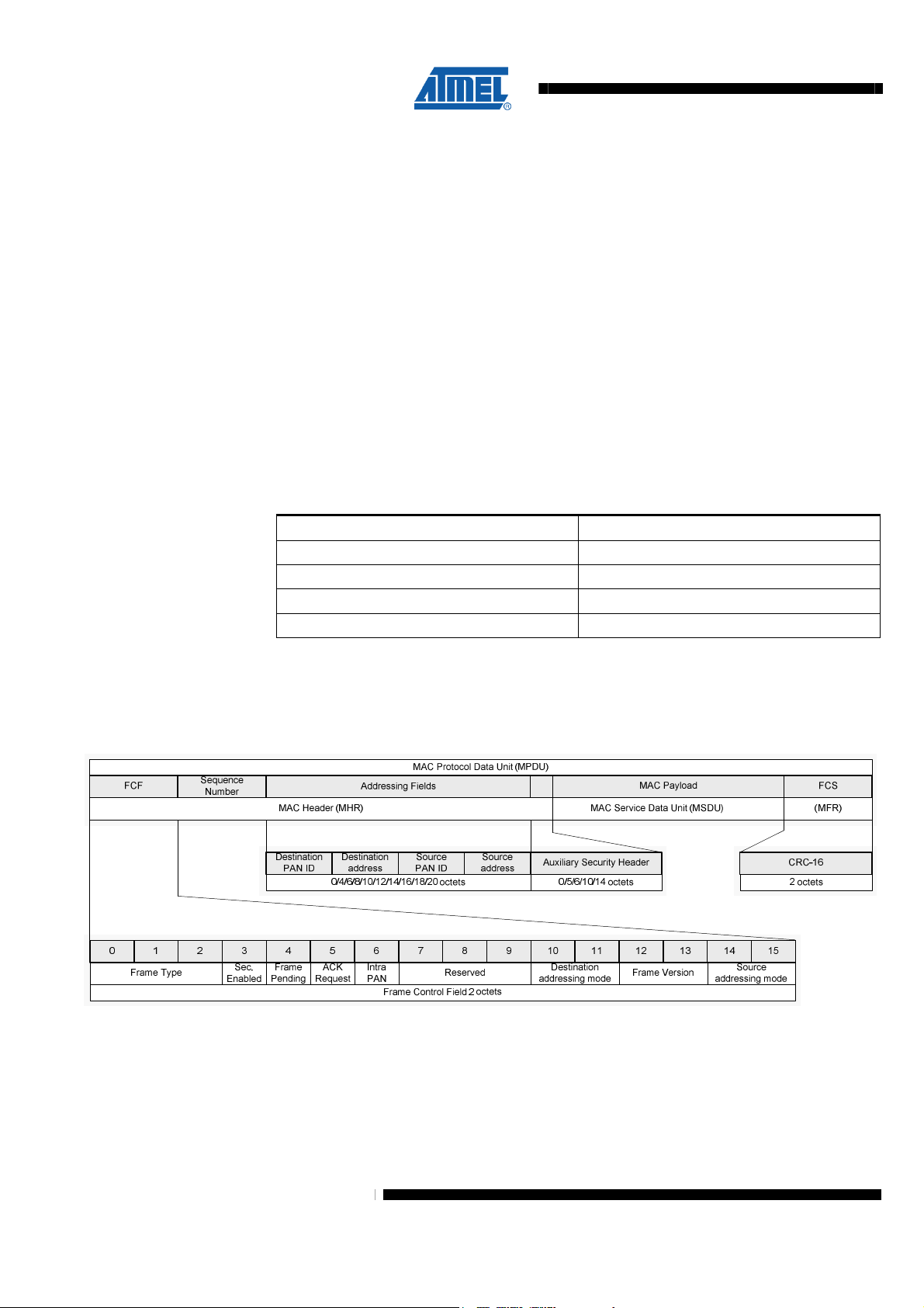
ATmega128RFA1
On receive the PHR is returned as the first octet during Frame Buffer read access.
Even though the standard only defines frame lengths ≤127 bytes, the radio transceiver
is able to transmit and receive frame length values >127. For IEEE 802.15.4 compliant
operation bit 8 has to be masked by software. The reception of a valid PHR is signaled
by a TRX24_RX_START interrupt.
On transmit the PHR has to be written first to the Frame Buffer.
9.5.1.1.3 PHY Payload (PHY Service Data Unit, PSDU)
The PSDU has a variable length between 0 and aMaxPHYPacketSize (127, maximum
PSDU size in octets) whereas the last two octets are used for the Frame Check
Sequence (FCS). The length of the PSDU is signaled by the frame length field (PHR)
as described in
Unit (MPDU).
Received frames with a frame length field set to 0x00 (invalid PHR) are not by an
interrupt.
Table 9-15 below summarizes the type of payload versus the frame length value.
Table 9-15. Frame Length Field - PHR
9.5.1.2 MAC Protocol Layer Data Unit (MPDU)
Figure 9-15 below shows the frame structure of the MAC layer.
Figure 9-15. IEEE 802.15.4 Frame Format - MAC-Layer Frame Structure (MPDU)
Table 9-15 below. The PSDU contains the MAC Protocol Layer Data
Frame Length Value Payload
0 - 4 Reserved
6 – 8 Reserved
9 - aMaxPHYPacketSize MPDU
5 MPDU (Acknowledgement)
9.5.1.2.1 MAC Header (MHR) Fields
The MAC header consists of the Frame Control Field (FCF), a sequence number, and
the addressing fields (which are of variable length and can even be empty in certain
situations).
62
8266A-MCU Wireless-12/09
Page 63
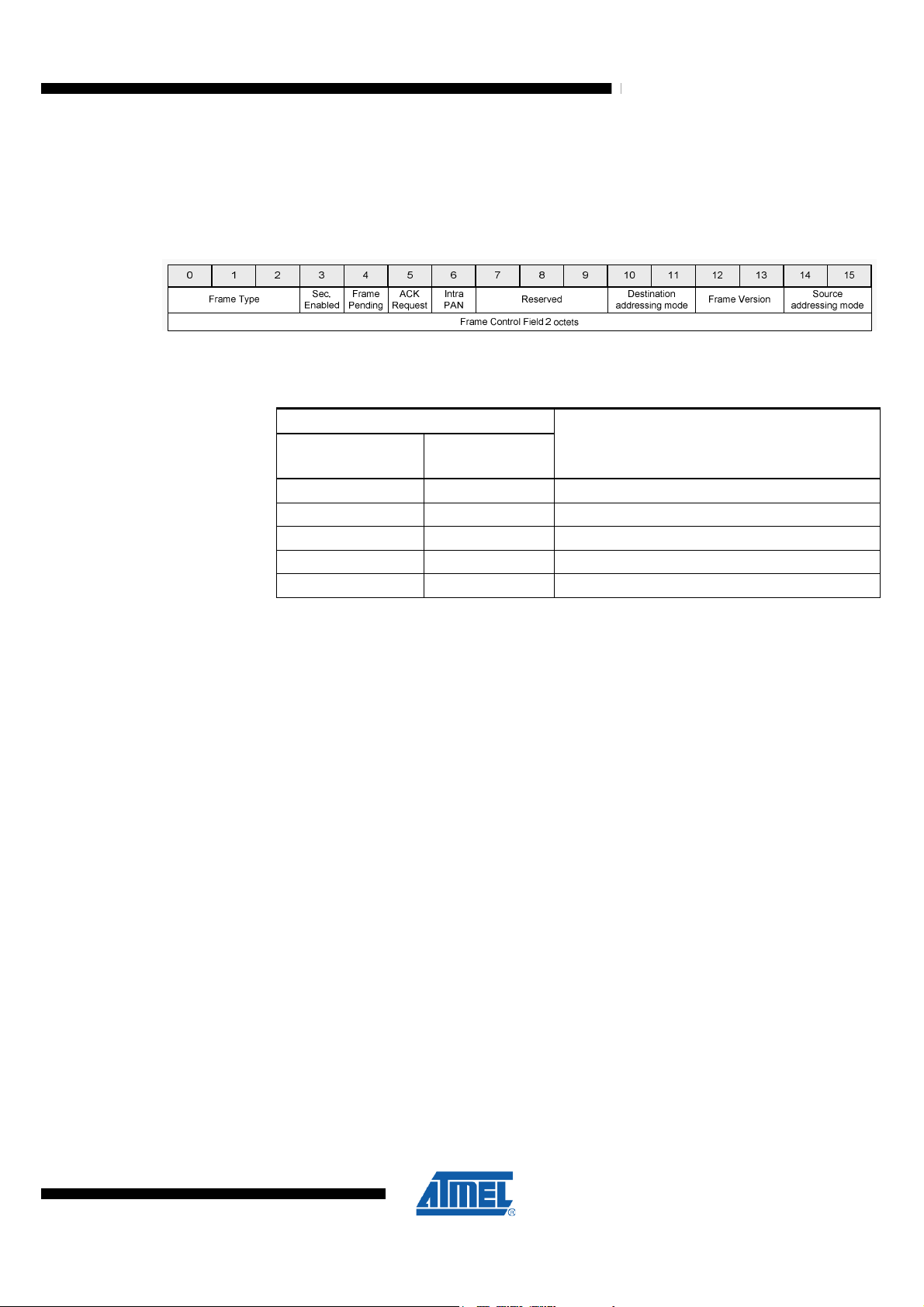
ATmega128RFA1
9.5.1.2.2 Frame Control Field (FCF)
The FCF consists of 16 bits, and occupies the first two octets of either the MPDU or the
PSDU, respectively.
Figure 9-26. IEEE 802.15.4-2006 Frame Control Field (FCF)
Bit [2:0]: describe the frame type. Table 9-16 below summarizes frame types defined
by IEEE 802.15.4, section 7.2.1.1.1.
Table 9-16. Frame Control Field – Frame Type Subfield
Frame Control Field Bit Assignments
Frame Type Value
b2 b1 b0
000 0 Beacon
001 1 Data
010 2 Acknowledge
011 3 MAC command
100 – 111 4 – 7 Reserved
This subfield is used for address filtering by the third level filter rules. Only frame types
0 – 3 pass the third level filter rules (refer to section "Frame Filtering" on page 54).
Automatic address filtering of the radio transceiver is enabled when using the
RX_AACK mode (refer to "RX_AACK_ON – Receive with Automatic ACK" on page 46).
A reserved frame (frame type value > 3) can be received if bit AACK_UPLD_RES_FT of
register XAH_CTRL_1 is set. For details refer to chapter "Configuration of non IEEE
802.15.4 Compliant Scenarios" on page 52. Address filtering is also provided in Basic
Operating Mode as explained in "Basic Operating Mode" on page 35.
Bit 3: indicates whether security processing applies to this frame.
Bit 4: is the “Frame Pending” subfield. This field can be set in an acknowledgment
frame (ACK) in response to a data request MAC command frame. This bit indicates that
the node, which transmitted the ACK, has more data to send to the node receiving the
ACK.
Value
Description
8266A-MCU Wireless-12/09
For acknowledgment frames automatically generated by the radio transceiver, this bit is
set according to the content of bit AACK_SET_PD of register CSMA_SEED_1 if the
received frame was a data request MAC command frame.
Bit 5: forms the “Acknowledgment Request” subfield. If this bit is set within a data or
MAC command frame that is not broadcast, the recipient shall acknowledge the
reception of the frame within the time specified by IEEE 802.15.4 (i.e. within 192 µs for
non beacon-enabled networks).
The radio transceiver parses this bit during RX_AACK mode and transmits an
acknowledgment frame if necessary.
In TX_ARET mode this bit indicates if an acknowledgement frame is expected after
transmitting a frame. If this is the case, the receiver waits for the acknowledgment
frame, otherwise the TX_ARET transaction is finished.
63
Page 64
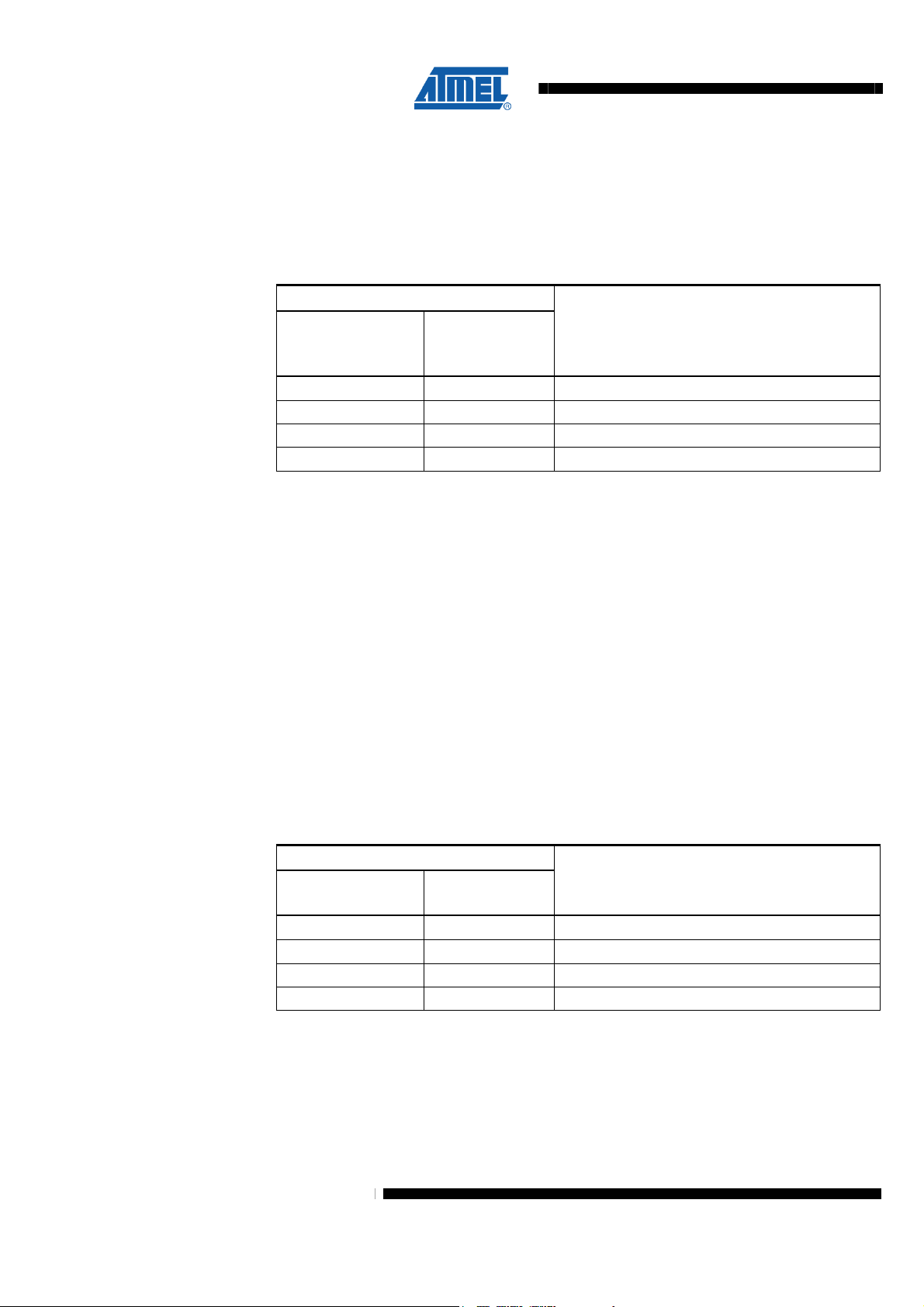
ATmega128RFA1
Bit 6: the “Intra-PAN” subfield indicates that in a frame, where both, the destination and
source addresses are present, the PAN-ID of the source address filed is omitted. In
RX_AACK mode this bit is evaluated by the address filter logic of the radio transceiver.
Bit [11:10]: the “Destination Addressing Mode” subfield describes the format of the
destination address of the frame. The values of the address modes are summarized in
Table 9-17 below according to IEEE 802.15.4:
Table 9-17. Frame Control Field – Destination and Source Addressing Mode
Frame Control Field Bit Assignments
Addressing Mode
b11 b
10
b15 b
14
00 0 PAN identifier and address fields are not present
01 1 Reserved
10 2 Address field contains a 16-bit short address
11 3 Address field contains a 64-bit extended address
If the destination address mode is either 2 or 3 (i.e. if the destination address is
present), it always consists of a 16-bit PAN-ID first followed by either the 16-bit or 64-bit
address as defined by the mode.
Value
Description
Bit [13:12]: the “Frame Version” subfield specifies the version number corresponding to
the frame. These register bits are reserved in IEEE-802.15.4-2003.
This subfield shall be set to 0 to indicate a frame compatible with IEEE 802.15.4-2003
and 1 to indicate an IEEE 802.15.4-2006 frame. All other subfield values shall be
reserved for future use.
The bit AACK_FVN_MODE of register CSMA_SEED_1 controls the RX_AACK
behavior of frame acknowledgements. This register determines if, depending on the
Frame Version Number, a frame is acknowledged or not. This is necessary for
backward compatibility to IEEE 802.15.4-2003 and for future use. Even if frame version
numbers 2 and 3 are reserved, it can be handled by the radio transceiver. For details
refer to "CSMA_SEED_1 – Transceiver Acknowledgment Frame Control Register 2" on
page 129.
See IEEE 802.15.4-2006, section 7.2.3 for details on frame compatibility.
Table 9-18. Frame Control Field – Frame Version Subfield
Frame Control Field Bit Assignments
Frame Version
b13 b12
00 0 Frames are compatible with IEEE 802.15.4-2003
01 1 Frames are compatible with IEEE 802.15.4-2006
10 2 Reserved
11 3 Reserved
Description
Value
64
Bit [15:14]: the “Source Addressing Mode” subfield, with similar meaning as
“Destination Addressing Mode” (refer to Table 9-17 above).
The subfields of the FCF (Bits 0–2, 3, 6, 10–15) affect the address filter logic of the
radio transceiver while executing a RX_AACK operation (see "RX_AACK_ON –
Receive with Automatic ACK" on page 46).
8266A-MCU Wireless-12/09
Page 65

ATmega128RFA1
9.5.1.2.3 Frame Compatibility between IEEE 802.15.4-2003 and IEEE 802.15.4-2006
All unsecured frames according to IEEE 802.15.4-2006 are compatible with unsecured
frames compliant with IEEE 802.15.4-2003 with two exceptions: a coordinator
realignment command frame with the “Channel Page” field present (see IEEE 802.15.42006 7.3.8) and any frame with a MAC Payload field larger than
aMaxMACSafePayloadSize octets.
Compatibility for secured frames is shown in the following table, which identifies the
security operating modes for IEEE 802.15.4-2006.
Table 9-19. Frame Control Field – Security and Frame Version
Frame Control Field Bit Assignments
Security Enabled
b3
0 00 No security. Frames are compatible between
0 01 No security. Frames are not compatible between
1 00 Secured frame formatted according to
1 01 Secured frame formatted according to
Description
Frame Version
b13 b12
IEEE 802.15.4-2003 and IEEE 802.15.4-2006.
IEEE 802.15.4-2003 and IEEE 802.15.4-2006.
IEEE 802.15.4-2003. This frame type is not
supported in IEEE 802.15.4-2006.
IEEE 802.15.4-2006
9.5.1.2.4 Sequence Number
The one-octet sequence number following the FCF identifies a particular frame, so that
duplicated frame transmissions can be detected. While operating in RX_AACK mode,
the content of this field is copied from the frame to be acknowledged into the
acknowledgment frame.
9.5.1.2.5 Addressing Fields
The addressing fields of the MPDU are used by the radio transceiver for address
matching indication. The destination address (if present) is always first, followed by the
source address (if present). Each address field consists of the Intra PAN-ID and a
device address. If both addresses are present and the “Intra PAN-ID compression”
subfield in the FCF is set to one, the source Intra PAN-ID is omitted.
Note that in addition to these general rules IEEE 802.15.4 further restricts the valid
address combinations for the individual possible MAC frame types. For example the
situation where both addresses are omitted (source addressing mode = 0 and
destination addressing mode = 0) is only allowed for acknowledgment frames. The
address filter in the radio transceiver has been designed to apply to IEEE 802.15.4
compliant frames. It can be configured to handle other frame formats and exceptions.
9.5.1.2.6 Auxiliary Security Header Field
The Auxiliary Security Header specifies information required for security processing and
has a variable length. This field determines how the frame is actually protected (security
level) and which keying material from the MAC security PIB is used (see
IEEE 802.15.4-2006, 7.6.1). This field shall be present only if the Security Enabled
8266A-MCU Wireless-12/09
65
Page 66

ATmega128RFA1
subfield b3 is set to one (see section
2003 and IEEE 802.15.4-2006" on page 65). For details of its structure see
IEEE 802.15.4-2006, 7.6.2 Auxiliary security header.
9.5.1.2.7 MAC Service Data Unit (MSDU)
This is the actual MAC payload. It is usually structured according to the individual frame
type. A description can be found in IEEE 802.15.4-2006, chapter 5.5.3.2.
9.5.1.2.8 MAC Footer (MFR) Fields
The MAC footer consists of a two-octet Frame Checksum (FCS). For details refer to the
following section "Frame Check Sequence (FCS)" below.
"Frame Compatibility between IEEE 802.15.4-
9.5.2 Frame Check Sequence (FCS)
The Frame Check Sequence (FCS) is characterized by:
• Indicate bit errors based on a cyclic redundancy check (CRC) of 16 bit length;
• Uses International Telecommunication Union (ITU) CRC polynomial;
• Automatically evaluated during reception;
• Can be automatically generated during transmission.
9.5.2.1 Overview
The FCS is intended for use at the MAC layer to detect corrupted frames at a first level
of filtering. It is computed by applying an ITU CRC polynomial to all transferred bytes
following the length field (MHR and MSDU fields). The frame check sequence has a
length of 16 bit and is located in the last two bytes of a frame (MAC footer, see Figure
9-15 on page 62).
The radio transceiver applies an FCS check on each received frame. The result of the
FCS check is stored in bit RX_CRC_VALID of register PHY_RSSI.
On transmit the radio transceiver generates and appends the FCS bytes during the
frame transmission. This behavior can be disabled by setting the bit
TX_AUTO_CRC_ON = 0 in register TRX_CTRL_1.
9.5.2.2 CRC calculation
The CRC polynomial used in IEEE 802.15.4 networks is defined by
The FCS shall be calculated for transmission using the following algorithm:
Let
be the polynomial representing the sequence of bits for which the checksum is to be
computed. Multiply M(x) by x16 giving the polynomial
Divide
polynomial
The FCS field is given by the coefficients of the remainder polynomial, R(x).
51216
1)(
kk
1
14
+++= xxxxG
2
−−
...)( rxrxrxrxR ++++=
1514
++++=
bxbxbxbxM K
12
−−
kk
16
0
0
15
1
16
)()( xxMxN ⋅=
1
)(
modulo 2 by the generator polynomial G16(x) to obtain the remainder
)(xN
66
8266A-MCU Wireless-12/09
Page 67

ATmega128RFA1
9.5.2.3 Automatic FCS generation
Example:
Consider a 5 octet ACK frame. The MHR field consists of
0100 0000 0000 0000 0101 0110.
The leftmost bit (b0) is transmitted first in time. The FCS is in this case
0010 0111 1001 1110.
The leftmost bit (r0) is transmitted first in time.
The automatic FCS generation is performed with register bit TX_AUTO_CRC_ON = 1
(reset value). This allows the radio transceiver to autonomously compute the FCS. For
a frame with a frame length specified as N (3 ≤ N ≤ 127), the FCS is calculated on the
first N-2 octets in the Frame Buffer and the resulting FCS field is transmitted in place of
the last two octets from the Frame Buffer.
If the automatic FCS generation of the radio transceivers is enabled, the Frame Buffer
write access can be stopped right after MAC payload. There is no need to write FCS
dummy bytes.
In RX_AACK mode, when a received frame needs to be acknowledged, the FCS of the
ACK frame is always automatically generated by the radio transceiver, independent of
the TX_AUTO_CRC_ON setting.
Example:
A frame transmission of length five with TX_AUTO_CRC_ON set, is started with a
Frame Buffer write access of five bytes (the last two bytes can be omitted). The first
three bytes are used for FCS generation; the last two bytes are replaced by the
internally calculated FCS.
9.5.2.4 Automatic FCS check
An automatic FCS check is applied on each received frame with a frame length N ≥ 2.
The bit RX_CRC_VALID of register PHY_RSSI is set if the FCS of a received frame is
valid. The register bit is updated when issuing a TRX24_RX_END interrupt and remains
valid until a new frame reception causes the next TRX24_RX_END interrupt.
In RX_AACK mode, the radio transceiver rejects the frame and the TRX24_RX_END
interrupt is not issued if the FCS of the received frame is not valid.
In TX_ARET mode, the FCS and the sequence number of an ACK are automatically
checked. The ACK is not accepted if one of those is not correct.
9.5.3 Received Signal Strength Indicator (RSSI)
The Received Signal Strength Indicator is characterized by:
• Minimum RSSI level is -90 dBm (RSSI_BASE_VAL);
• Dynamic range is 81 dB;
• Minimum RSSI value is 0;
• Maximum RSSI value is 28.
9.5.3.1 Overview
8266A-MCU Wireless-12/09
The RSSI is a 5-bit value indicating the receive power in the selected channel in steps
of 3 dB. No attempt is made to distinguish IEEE 802.15.4 signals from others. Only the
67
Page 68

ATmega128RFA1
9.5.3.2 Reading RSSI
9.5.3.3 Data Interpretation
received signal strength is evaluated. The RSSI provides the basis for an ED
measurement. See section
In Basic Operating Mode the RSSI value is valid in any receive state, and is updated
every t
It is not recommended to read the RSSI value when using the Extended Operating
Mode. The automatically generated ED value should then be used (see section "Energy
Detection (ED)" below).
The RSSI value is a 5-bit value indicating the receive power in steps of 3 dB and with a
range of 0- 28.
= 2 µs to register PHY_RSSI.
TR25
"Energy Detection (ED)" below for details.
An RSSI value of 0 indicates a receiver RF input power of P
value in the range of 1 to 28, the RF input power can be calculated as follows:
PRF = RSSI_BASE_VAL + 3 • (RSSI - 1) [dBm]
Figure 9-17. Mapping between RSSI Value and Received Input Power
< -90 dBm. For an RSSI
RF
9.5.4 Energy Detection (ED)
10
0
-10
-20
[dBm]
RF
-30
-40
-50
-60
-70
-80
Receiver Input Power P
-90
-100
0 2 4 6 8 10 12 14 16 18 20 22 24 26 28 30
Measured
Ideal
RSSI
The Energy Detection (ED) module is characterized by:
• 85 unique energy levels defined;
• 1 dB resolution.
9.5.4.1 Overview
68
The receiver ED measurement is used by the network layer as part of a channel
selection algorithm. It is an estimation of the received signal power within the bandwidth
of an IEEE 802.15.4 channel. No attempt is made to identify or decode signals on the
channel. The ED value is calculated by averaging RSSI values over eight symbols
(128 µs).
8266A-MCU Wireless-12/09
Page 69

ATmega128RFA1
9.5.4.2 Measurement Description
For High Data Rate Modes the automated ED measurement duration is reduced to
32 µs as described in "High Data Rate Modes" on page 86. The measurement period in
these modes is still 128 µs for manually initiated ED measurements as long as the
receiver is in RX_ON state.
There are two ways to initiate an ED measurement:
• Manually, by writing an arbitrary value to register PHY_ED_LEVEL, or
• Automatically, after detection of a valid SHR of an incoming frame.
For manually initiated ED measurements the radio transceiver needs to be in one of the
states RX_ON or BUSY_RX. The end of the ED measurement is indicated by a
TRX24_CCA_ED_DONE interrupt.
The automatic ED measurement is started if a SHR is detected. The end of the
automatic measurement is not signaled by an interrupt.
The measurement result is stored after t
and processing delay) in register PHY_ED_LEVEL.
Thus by using Basic Operating Mode a valid ED value from the currently received frame
is accessible 108 µs after the TRX24_RX_START interrupt and remains valid until the
next incoming frame generates a new TRX24_RX_START interrupt or until another ED
measurement is initiated.
When using the Extended Operating Mode it is recommended to mask the
TRX24_RX_START interrupt. Hence the interrupt cannot be used as timing reference.
A successful frame reception is signalized by the TRX24_RX_END interrupt. The
minimum time span between a TRX24_RX_END interrupt and a following SFD
detection is t
within 224 µs including the ED measurement time after the TRX24_RX_END interrupt.
Otherwise it could be overwritten by the result of the next measurement cycle. This is
important for time critical applications or if the TRX24_RX_START interrupt is not used
to indicate the reception of a frame.
= 96 µs due to the length of the SHR. The ED value needs to be read
TR27
= 140 µs (128 µs measurement duration
TR26
9.5.4.3 Data Interpretation
8266A-MCU Wireless-12/09
The values of the register PHY_ED_LEVEL are:
Table 9-20. Register Bit PHY_ED_LEVEL Interpretation
PHY_ED_LEVEL Description
0xFF Reset value
0x00 … 0x54 ED measurement result of the last ED measurement
Note: 1. It is not recommended to manually initiate an ED measurement when using the
Extended Operating Mode.
The PHY_ED_LEVEL is an 8-bit register. The ED value of the radio transceiver has a
valid range from 0x00 to 0x54 with a resolution of 1 dB. All other values do not occur. A
value of 0xFF indicates the reset value. A value of PHY_ED_LEVEL = 0 indicates that
the measured energy is less than -90 dBm (see parameter RSSI_BASE_VAL in section
"Receiver Characteristics" on page 508). Due to environmental conditions (temperature,
voltage, semiconductor parameters etc.) the calculated ED value has a maximum
tolerance of ±5 dB, this is to be considered as constant offset over the measurement
range.
An ED value of 0 indicates an RF input power of PRF ≤ -90 dBm. For an ED value in the
range of 0 to 84, the RF input power can be calculated as follows:
69
Page 70

ATmega128RFA1
Register PHY_ED_LEVEL Value
PRF = -90 + ED [dBm]
Figure 9-18. Mapping between values in PHY_ED_LEVEL and Received Input Power
10
9.5.4.4 Interrupt Handling
0
-10
-20
[dBm]
RF
-30
-40
-50
-60
-70
-80
Receiver Input Power P
-90
-100
0 10 20 30 40 50 60 70 80 90
Measured
Ideal
The TRX24_CCA_ED_DONE interrupt is issued at the end of a manually initiated ED
measurement.
Note that an ED request should only be initiated in one of the receive states. Otherwise
the radio transceiver generates a TRX24_CCA_ED_DONE interrupt but no ED
measurement was performed.
9.5.5 Clear Channel Assessment (CCA)
The main features of the Clear Channel Assessment (CCA) module are:
• All 4 modes are available as defined by IEEE 802.15.4-2006 in section 6.9.9;
• Adjustable threshold for energy detection algorithm.
9.5.5.1 Overview
A CCA measurement is used to detect a clear channel. Four modes are specified by
IEEE 802.15.4-2006:
Table 9-21. CCA Mode Overview
CCA Mode Description
1 Energy above threshold.
2 Carrier sense only.
70
CCA shall report a busy medium upon detecting any energy above the ED
threshold.
CCA shall report a busy medium only upon the detection of a signal with the
modulation and spreading characteristics of an IEEE 802.15.4 compliant signal.
The signal strength may be above or below the ED threshold.
8266A-MCU Wireless-12/09
Page 71

ATmega128RFA1
CCA Mode Description
9.5.5.2 Configuration and CCA Request
The CCA modes are configurable via register PHY_CC_CCA.
Usimg the Basic Operating Mode, a CCA request can be initiated manually by setting
CCA_REQUEST = 1 of register PHY_CC_CCA, if the radio transceiver is in any RX
state. The current channel status (CCA_STATUS) and the CCA completion status
(CCA_DONE) are accessible in register TRX_STATUS.
The CCA evaluation is done over eight symbol periods and the result is accessible
t
= 140 µs (128 µs measurement duration and processing delay) after the request.
TR28
The end of a manually initiated CCA measurement is indicated by a
TRX24_CCA_ED_DONE interrupt.
0, 3 Carrier sense with energy above threshold.
CCA shall report a busy medium using a logical combination of
- Detection of a signal with the modulation and spreading characteristics of
this standard and
- Energy above the ED threshold.
Where the logical operator may be configured as either OR (mode 0) or
AND (mode 3).
9.5.5.3 Data Interpretation
9.5.5.4 Interrupt Handling
The sub-register CCA_ED_THRES of register CCA_THRES defines the received power
threshold of the “energy above threshold” algorithm. The threshold is calculated by
RSSI_BASE_VAL + 2 • CCA_ED_THRES [dBm]. Any received power above this level
is interpreted as a busy channel.
Note that it is not recommended to manually initiate a CCA measurement when using
the Extended Operating Mode.
The current channel status (CCA_STATUS) and the CCA completion status
(CCA_DONE) are accessible in register TRX_STATUS. Note, register bits CCA_DONE
and CCA_STATUS are cleared in response to a CCA_REQUEST.
The completion of a measurement cycle is indicated by CCA_DONE = 1. If the radio
transceiver detected no signal (idle channel) during the measurement cycle, the
CCA_STATUS bit is set to 1.
When using the “energy above threshold” algorithm, any received power above
CCA_ED_THRES level is interpreted as a busy channel. The “carrier sense” algorithm
reports a busy channel when detecting an IEEE 802.15.4 signal above the
RSSI_BASE_VAL (see parameter RSSI_BASE_VAL in "Transceiver Electrical
Characteristics" on page 507). The radio transceiver is also able to detect signals below
this value, but the detection probability decreases with the signal power.
8266A-MCU Wireless-12/09
The TRX24_CCA_ED_DONE interrupt is issued at the end of a manually initiated CCA
measurement.
Note: A CCA request should only be initiated in the receive states of Basic Operating Mode.
Otherwise the radio transceiver generates a TRX24_CCA_ED_DONE interrupt and
sets the register bit CCA_DONE = 1 even if no CCA measurement was performed.
71
Page 72

ATmega128RFA1
9.5.5.5 Measurement Time
The response time for a manually initiated CCA measurement depends on the receiver
state.
In RX_ON state the CCA measurement is done over eight symbol periods and the
result is accessible 140 µs after the request (see section
Request" on page 71).
"Configuration and CCA
In BUSY_RX state the CCA measurement duration depends on the CCA Mode and the
CCA request relative to the reception of an SHR. The end of the CCA measurement is
indicated by a TRX24_CCA_ED_DONE interrupt. The variation of a CCA measurement
period in BUSY_RX state is described in Table 9-22 below.
Table 9-22. CCA Measurement Period and Access in BUSY_RX state
CCA Mode Request within ED measurement
Energy above threshold. 1
CCA result is available after finishing
automated ED measurement period.
Carrier sense only. 2
CCA result is immediately available after request.
Carrier sense with Energy above threshold (AND). 3
CCA result is available after finishing
automated ED measurement period.
Carrier sense with Energy above threshold (OR). 0
CCA result is available after finishing
automated ED measurement period.
Note: 1. After receiving the SHR an automated ED measurement is started with a length of
8 symbol periods (PSDU rate 250 kb/s), refer to section "Energy Detection (ED)"
on page 68. This automated ED measurement must be finished to provide a result
for the CCA measurement. Only one automated ED measurement per frame is
performed.
(1)
Request after ED measurement
CCA result is immediately available
after request.
CCA result is immediately available
after request.
CCA result is immediately available
after request.
It is recommended to perform CCA measurements in RX_ON state only. To avoid
accidental switching to BUSY_RX state the SHR detection can be disabled by setting
bit RX_PDT_DIS of register RX_SYN. Refer to section "Receiver (RX)" on page 74 for
details. The receiver remains in RX_ON state to perform a CCA measurement until the
register bit RX_PDT_DIS is set back to continue the frame reception. In this case the
CCA measurement duration is 8 symbol periods.
9.5.6 Link Quality Indication (LQI)
According to IEEE 802.15.4 the LQI measurement is a characterization of the strength
and/or quality of a received packet. The measurement may be implemented using
receiver ED, a signal-to-noise ratio estimation or a combination of these methods. The
use of the LQI result by the network or application layers is not specified in this
standard. LQI values shall be an integer ranging from 0x00 to 0xFF. The minimum and
maximum LQI values (0x00 and 0xFF) should be associated with the lowest and
highest quality compliant signals, respectively, and LQI values in between should be
uniformly distributed between these two limits.
9.5.6.1 Overview
The LQI measurement of the radio transceiver is implemented as a measure of the link
quality which can be described with the packet error rate (PER) of this link. A LQI value
72
8266A-MCU Wireless-12/09
Page 73

ATmega128RFA1
can be associated with an expected packet error rate. The PER is the ratio of erroneous
LQI
received frames to the total number of received frames. A PER of zero indicates no
frame error whereas at a PER of one no frame was received correctly.
The radio transceiver uses correlation results of multiple symbols within a frame to
determine the LQI value. This is done for each received frame. The minimum frame
length for a valid LQI value is two octets PSDU. LQI values are integers ranging from 0
to 255.
The following figure shows an example of a conditional packet error rate when receiving
a certain LQI value.
Figure 9-19. Conditional Packet Error Rate versus LQI
1
0.9
0.8
0.7
0.6
0.5
PER
0.4
0.3
0.2
0.1
0
0 50 100 150 200 250
The values are taken from received frames of PSDU length of 20 octets on
transmission channels with reasonable low multipath delay spreads. If the transmission
channel characteristic has a higher multipath delay spread than assumed in the
example, the PER is slightly higher for a certain LQI value. Since the packet error rate
is a statistical value, the PER shown in Figure 9-19 above is based on a huge number
of transactions. A reliable estimation of the packet error rate cannot be based on a
single or a small number of LQI values.
9.5.6.2 Request a LQI Measurement
9.5.6.3 Data Interpretation
8266A-MCU Wireless-12/09
The LQI byte can be obtained after a frame has been received by the radio transceiver.
One additional byte is automatically attached to the received frame containing the LQI
value. This information can also be read via Frame Buffer read access, see "User
accessible Frame Content" on page 78. The LQI byte can be read after the
TRX24_RX_END interrupt.
According to IEEE 802.15.4 a low LQI value is associated with low signal strength
and/or high signal distortions. Signal distortions are mainly caused by interference
signals and/or multipath propagation. High LQI values indicate a sufficient high signal
power and low signal distortions.
73
Page 74
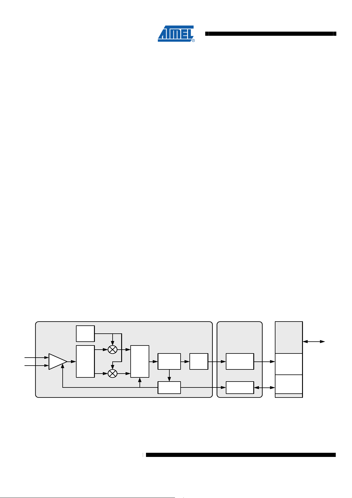
ATmega128RFA1
Note that the received signal power as indicated by the received signal strength
indication (RSSI) value or energy detection (ED) value of the radio transceiver do not
characterize the signal quality and the ability to decode a signal.
As an example, a received signal with an input power of about 6 dB above the receiver
sensitivity likely results in a LQI value close to 255 for radio channels with very low
signal distortions. For higher signal power the LQI value becomes independent of the
actual signal strength. This is because the packet error rate for these scenarios tends
towards zero and further increased signal strength i.e. increasing the transmission
power does not decrease the error rate any further. In this case RSSI or ED can be
used to evaluate the signal strength and the link margin.
ZigBee networks often require the identification of the “best” routing between two
nodes. Both the LQI and the RSSI/ED can be used for this, dependent on the
optimization criteria. If a low packet error rate (corresponding to high throughput) is the
optimization criteria then the LQI value should be taken into consideration. If a low
transmission power or the link margin is the optimization criteria then the RSSI/ED
value is also helpful.
Combinations of LQI, RSSI and ED are possible for routing decisions. As a rule of
thumb RSSI and ED values are useful to differentiate between links with high LQI
values. Transmission links with low LQI values should be discarded for routing
decisions even if the RSSI/ED values are high. This is because RSSI and ED do not
say anything about the possibility to decode a signal. It is only an information about the
received signal strength whereas the source can be an interferer.
9.6 Module Description
9.6.1 Receiver (RX)
9.6.1.1 Overview
The receiver is split into an analog radio front-end and a digital base band processor
(RX BBP) according to the following figure. The digital base band processor and the
control engine are connected to the Frame Buffer and control registers which are
located in the microcontroller I/O memory space (see
"Transceiver to Microcontroller Interface" on page 31 ).
Figure 9-20. Receiver Block Diagram
LO
RFP
LN A PP F BP F L im iter
RFN
The differential RF signal is amplified by a low noise amplifier (LNA), filtered (PPF) and
down converted to an intermediate frequency by a mixer. Channel selectivity is
performed using an integrated band pass filter (BPF). A limiting amplifier (Limiter)
provides sufficient gain to overcome the DC offset of the succeeding analog-to-digital
An a log Dom a in D igita l Dom a in
AG C
RX
AD C
RSS I
RX BB P
Con trol
"I/O Memory" on page 25 and
I/O
Mem ory
Sp a ce
$0 1FF
Fr am e
B uf fe r
$0 180
$0 17F
Re g ist ers
$0 140
µC
I/F
74
8266A-MCU Wireless-12/09
Page 75

ATmega128RFA1
converter (RX ADC) and generates a digital RSSI signal. The ADC output signal is
sampled and processed further by the digital base band receiver (RX BBP).
The RX BBP performs additional signal filtering and signal synchronization. The
frequency offset of each frame is calculated by the synchronization unit and is used
during the remaining receive process to correct the offset. The receiver is designed to
handle frequency and symbol rate deviations up to ±120 ppm caused by combined
receiver and transmitter deviations. For details refer to chapter "General RF
Specifications" on page 507. Finally the signal is demodulated and the data are stored
in the Frame Buffer.
In Basic Operating Mode (see "Basic Operating Mode" on page 35), the reception of a
frame is indicated by a TRX24_RX_START interrupt. Accordingly its end is signalized
by a TRX24_RX_END interrupt. Based on the quality of the received signal a link
quality indicator (LQI) is calculated and appended to the frame. For details refer to.
Additional signal processing is applied to the frame data to provide further status
information like ED value (register PHY_ED_LEVEL) and FCS correctness (register
PHY_RSSI).
Beyond these features the Extended Operating Mode of the radio transceiver supports
address filtering and pending data indication. For details refer to "Extended Operating
Mode" on page 43.
9.6.1.2 Frame Receive Procedure
9.6.1.3 Configuration
The frame receive procedure including the radio s setup for reception and reading
PSDU data from the Frame Buffer is described in "Frame Receive Procedure" on page
84.
In Basic Operating Mode the receiver is enabled by writing command RX_ON to the
TRX_CMD bits of register TRX_STATE in the states TRX_OFF or PLL_ON. Similarly in
Extended Operating Mode the receiver is enabled for RX_AACK operation from the
states TRX_OFF or PLL_ON by writing the command RX_AACK_ON. There is no
additional configuration required to receive IEEE 802.15.4 compliant frames when using
the Basic Operating Mode. However, the frame reception in the Extended Operating
Mode requires further register configurations. For details refer to "Extended Operating
Mode" on page 43.
The receiver has an outstanding sensitivity performance of -100 dBm. At certain
environmental conditions or for High Data Rate Modes (see "High Data Rate Modes" on
page 86) it may be useful to manually decrease this sensitivity. This is achieved by
adjusting the detector threshold of the synchronization header using the
RX_PDT_LEVEL bits of register RX_SYN. Received signals with a RSSI value below
the threshold do not activate the demodulation process.
Furthermore, it may be useful to protect a received frame against overwriting by
subsequent received frames.
8266A-MCU Wireless-12/09
A Dynamic Frame Buffer Protection is enabled with register bit RX_SAFE_MODE
(TRX_CTRL_2) set (refer to "Dynamic Frame Buffer Protection" on page 91). After a
frame has been received, the buffer is protected for new incoming frames and the
receiver remains in RX_ON or RX_AACK_ON state until the RX_SAFE_MODE bit is
cleared by the controller. The Frame Buffer content is only protected if the FCS is valid.
A Static Frame Buffer Protection is enabled with bit RX_PDT_DIS of register RX_SYN
set. The receiver remains in RX_ON or RX_AACK_ON state and no further SHR is
detected until the register bit RX_PDT_DIS is set back.
75
Page 76

ATmega128RFA1
9.6.2 Transmitter (TX)
9.6.2.1 Overview
The transmitter consists of a digital base band processor (TX BBP) and an analog front
end as shown in the following figure.
Figure 9-21. Transmitter Block Diagram
DIG3/4
RFP
Buf
RFN
Ex t. R F front-e nd an d
Outpu t Pow e r C on trol
PLL – T X M odu la tion PA
The TX BBP reads the frame data from the Frame Buffer and performs the bit-tosymbol and symbol-to-chip mapping as specified by IEEE 802.15.4 in section 6.5.2.
The O-QPSK modulation signal is generated and fed into the analog radio front end.
The fractional-N frequency synthesizer (PLL) converts the baseband transmit signal to
the RF signal which is amplified by the power amplifier (PA). The PA output is internally
connected to bidirectional differential antenna pins (RFP, RFN) so that no external
antenna switch is needed.
TX Data
Ana lo g D omain
$0 140
Co n trol
TX BB P
Digita l Dom a in
Reg is te rs
Frame
Buf fe r
I/O
Mem ory
Sp ace
$0 17F
$0 180
$0 1FF
µC
I/F
9.6.2.2 Frame Transmit Procedure
9.6.2.3 Configuration
9.6.2.4 TX Power Ramping
The frame transmit procedure including writing PSDU data in the Frame Buffer and
initiating a transmission is described in section "Frame Transmit Procedure" on page
84. The controller must ensure to provide valid frame data before starting the frame
transmission. For save operation, it is recommended to write the complete frame into
the Frame Buffer before starting the frame transmission.
The maximum output power of the transmitter is typically +3.5 dBm. The output power
can be configured via the TX_PWR bits of register PHY_TX_PWR. The output power of
the transmitter can be controlled over a 20 dB range.
A transmission can be started from PLL_ON or TX_ARET_ON state by writing ‘1’ to bit
SLPTR of the TRXPR register or by writing TX_START command to the TRX_CMD bits
of register TRX_STATE.
The PA buffer and PA are enabled sequentially to optimize the output power spectral
density (PSD). A timing example using default settings illustrates the sequence in the
next figure. In this example the transmission is initiated with the rising edge of the
SLPTR bit. The radio transceiver state changes from PLL_ON to BUSY_TX. The
modulation starts 16 µs after SLPTR.
76
8266A-MCU Wireless-12/09
Page 77
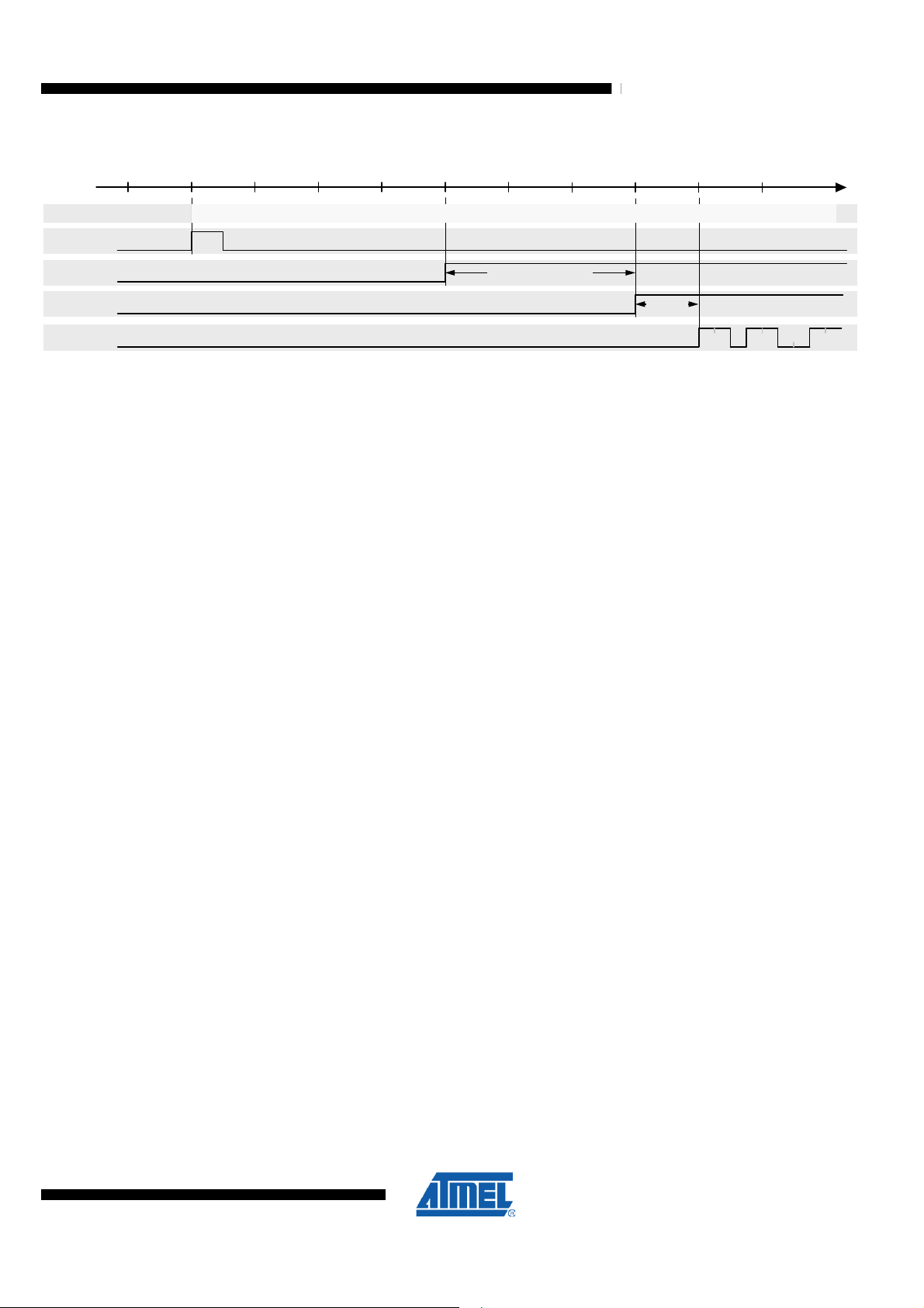
ATmega128RFA1
Figure 9-22. TX Power Ramping
0 6 8 10
2 12 14 16 18
4
Le ngth [µ s]
TR X _ ST A T E PL L_O N
SL P TR
PA bu ffer
PA
Mod ul at io n 1 1 1 1 1 10 00
When using an external RF front-end (refer to "RX/TX Indicator" on page 90) it may be
required to adjust the startup time of the external PA relative to the internal building
blocks to optimize the overall PSD. This can be achieved using register bits
PA_BUF_LT and PA_LT of register PHY_TX_PWR.
9.6.3 Frame Buffer
The radio transceiver contains a 128 byte dual port SRAM. One port of the frame buffer
is directly connected to the controller I/O space. Therefore random access to single
frame bytes is possible. The other port connects to the internal transmitter and receiver
modules. Both ports are independent and simultaneously accessible for data
communication.
The Frame Buffer uses the controller I/O address space 0x180 to 0x1FF for RX and TX
operation of the radio transceiver and can keep one IEEE 802.15.4 RX or one TX frame
of maximum length at a time.
Frame Buffer access is only possible if the radio transceiver is enabled (PRTRX24 bit in
the Power Reduction Register PRR1 is not set) and not in SLEEP state.
BU SY_ T X
PA _ BUF _LT
PA_LT
9.6.3.1 Data Management
Data in the Frame Buffer (received data or data to be transmitted) remain valid as long
as:
• No new frame or other data are written into the buffer;
• No new frame is received (in any BUSY_RX state);
• No state change into radio transceiver SLEEP state is made;
• No radio transceiver RESET (see bit TRXRST in "TRXPR – Transceiver Pin
Register" on page 169) or system reset took place;
• Bit PRTRX24 in register "PRR1 – Power Reduction Register 1" on page 168 is not
set;
By default there is no protection of the Frame Buffer against overwriting. If a frame is
received during a Frame Buffer read access of a previously received frame, the stored
data might be overwritten.
Finally the application software should check the transferred frame data integrity by a
FCS check.
The state of the radio transceiver should be changed to PLL_ON state after reception to
protect the Frame Buffer content against overwriting with new, incoming frames. This
can be achieved by writing immediately the command PLL_ON to the TRX_CMD bits of
register TRX_STATE after receiving the frame indicated by a TRX24_RX_END
interrupt.
8266A-MCU Wireless-12/09
77
Page 78
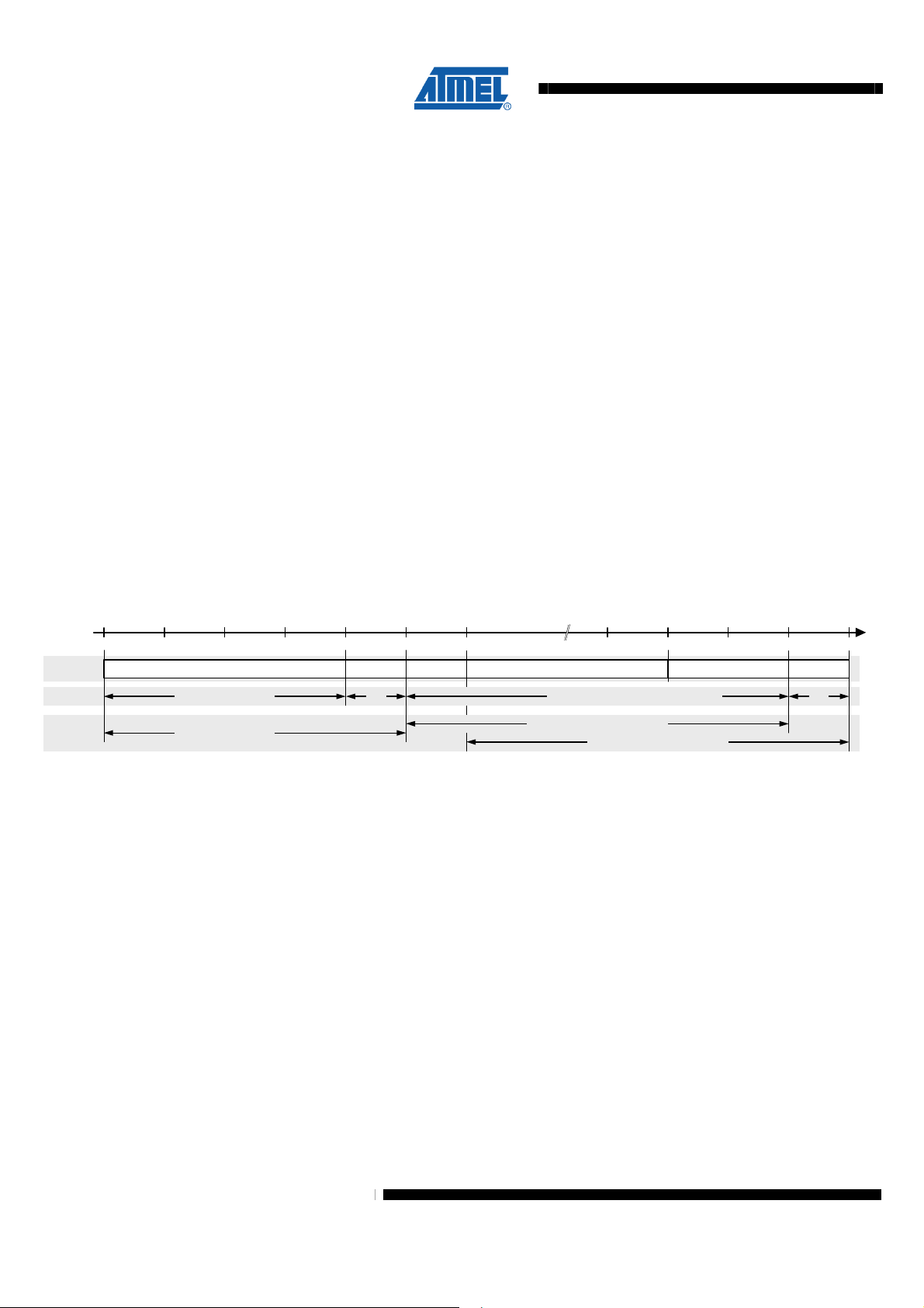
ATmega128RFA1
Alternatively Dynamic Frame Buffer Protection can be used to protect received frames
against overwriting. For details refer to
Both procedures do not protect the Frame Buffer from overwriting by the application
software.
In Extended Operating Mode during TX_ARET operation (see "TX_ARET_ON –
Transmit with Automatic Retry and CSMA-CA Retry" on page 57) the radio transceiver
switches to receive if an acknowledgement of a previously transmitted frame was
requested. During this period received frames are evaluated but not stored in the Frame
Buffer. This allows the radio transceiver to wait for an acknowledgement frame and
retry the frame transmission without writing the frame data to the Frame Buffer again.
A radio transceiver state change except a transition to radio transceiver SLEEP state or
a radio transceiver RESET does not affect the Frame Buffer content. The Frame Buffer
is powered off and the stored data gets lost if the radio transceiver is forced into radio
transceiver SLEEP state.
Access conflicts may occur when reading and writing data simultaneously at the two
independent ports of the Frame Buffer TX/RX BBP and Controller interface.
9.6.3.2 User accessible Frame Content
The radio transceiver supports an IEEE 802.15.4 compliant frame format as shown in
the following figure.
"Dynamic Frame Buffer Protection" on page 91.
Figure 9-31. Transceiver Frame Structure
0
Fra me
Durat ion 4 o cte ts / 1 28 µ s 1 y o cte ts / y • 32 µs (y <= 1 28 ) 1
Acces s
Len gth [octets]
Pre am ble S equence SF D P HR
SH R not a cce sible
PH Y generated
Notes: 1. Stored into Frame Buffer for TX operation
A frame comprises two sections. The radio transceiver internally generated SHR field
and the user accessible part are stored in the Frame Buffer. The SHR contains the
preamble and the SFD field. The variable frame section contains the PHR and the
PSDU including the FCS (see "Overview" on page 66).
The Frame Buffer content differs depending on the direction of the communication
(receive or transmit). To access the data follow the procedures described in "Radio
Transceiver Usage" on page 83.
During frame reception, the payload and the link quality indicator (LQI) value of a
successfully received frame are stored in the Frame Buffer. The radio transceiver
appends the LQI value to the frame data after the last received octet. Information of the
frame length is not stored in the Frame Buffer. The frame length information is located
in register TST_RX_LENGTH.
4 5 6 y + 3 y + 5 y + 6
(1)
2. Stored into Frame Buffer during frame reception.
Paylo ad L QI
TX : F rame B uff er conte nt
RX : Frame Buffer conte nt
FC S
(2)
78
The SHR (except the SFD used to generate the last octet of the SHR) can generally not
be read by the application software.
8266A-MCU Wireless-12/09
Page 79
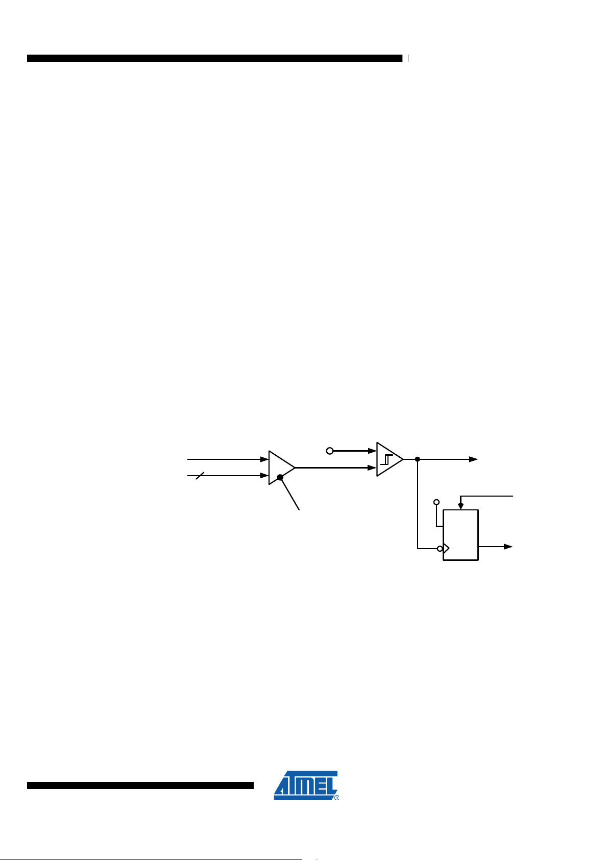
ATmega128RFA1
9.6.4 Battery Monitor (BATMON)
The PHR and the PSDU need to be stored in the Frame Buffer for frame transmission.
The PHR byte is the first byte in the Frame Buffer (address 0x180) and must be
calculated based on the PHR and the PSDU. The maximum frame size supported by
the radio transceiver is 128 bytes. If the TX_AUTO_CRC_ON bit is set in register
PHY_TX_PWR, the FCS field of the PSDU is replaced by the automatically calculated
FCS during frame transmission. There is no need to write the FCS field when using the
automatic FCS generation.
Manipulating individual bytes of the Frame Buffer is simply possible by accessing the
appropriate buffer address.
The minimum frame length supported by the radio transceiver for non IEEE 802.15.4
compliant frames is one byte (Frame Length Field + 1 byte of data).
9.6.4.1 Overview
The main features of the battery monitor are:
• Configurable voltage threshold range from 1.7V to 3.675V
• Generates an interrupt when supply voltage drops below the threshold
The battery monitor (BATMON) detects and indicates a low supply voltage of EVDD.
This is done by comparing the voltage of EVDD with a configurable, internal threshold
voltage. A simplified schematic of the BATMON with the most important input and
output signals is shown in the following figure.
Figure 9-24. Simplified Schematic of BATMON
BATMON_HR
4
BATMON_VTH
DAC
For input-to-output mapping
see BATMON register
EVDD
Threshold
Voltage
+
-
BATMON_OK
„1“
clear
D
Q
BATMON_IRQ
9.6.4.2 Configuration
9.6.4.3 Data Interpretation
8266A-MCU Wireless-12/09
The Battery Monitor can be configured using the BATMON register. Register subfield
BATMON_VTH sets the threshold voltage. It is configurable with a resolution of 75 mV
in the upper voltage range (BATMON_HR = 1) and with a resolution of 50 mV in the
lower voltage range (BATMON_HR = 0).
The bit BATMON_OK of register BATMON monitors the current value of the battery
voltage:
• If BATMON_OK = 0 then the battery voltage is lower than the threshold voltage;
• If BATMON_OK = 1 then the battery voltage is higher than the threshold voltage;
79
Page 80

ATmega128RFA1
9.6.4.4 Interrupt Handling
The value BATMON_OK should be read out to verify the current supply voltage value
after setting a new threshold.
Note: The battery monitor is inactive during SLEEP states. Refer to status register
TRX_STATUS for details.
A supply voltage drop below the configured threshold value is indicated by the
BAT_LOW interrupt. The BAT_LOW status bit as well as the BATLOW_EN bit is
located in the BATMON register. If BATLOW_EN =0, no IRQ is issued, but the status
flag is set if the battery low event occurs.
The interrupt is only issued if BATMON_OK changes from 1 to 0 and the event is stored
until the IRQ handler is called or the BAT_LOW IRQ is cleared manually by writing ‘1’ to
the BAT_LOW status flag.
No interrupt is generated when:
• The battery voltage is below the default 1.8V threshold at power up (BATMON_OK
was never 1) or
• A new threshold is set which is still above the current supply voltage (BATMON_OK
remains 0).
Noise or temporary voltage drops may generate unwanted interrupts when the battery
voltage is close to the programmed threshold voltage. To avoid this:
9.6.5 Crystal Oscillator (XOSC)
9.6.5.1 Overview
• Disable the BAT_LOW interrupt with the BATLOW_EN Bit in the BATMON register
and treat the battery as empty or
• Set a lower threshold value.
The main features of the crystal oscillator are:
• Amplitude controlled 16 MHz generation;
• 215 µs typical settling time after leaving SLEEP state;
• Configurable trimming with a capacitance array;
The crystal oscillator generates the reference frequency for the radio transceiver. All
other internally generated frequencies of the radio transceiver are derived from this
unique frequency. The overall system performance is therefore critically determined by
the accuracy of the crystal reference frequency. The external components of the crystal
oscillator should be selected carefully and the related board layout should be done with
caution as described in section
The register XOSC_CTRL provides access to the control signals of the oscillator. Two
operating modes are supported. It is recommended to use the integrated oscillator
setup as described in Figure 9-25 on page 81. Nevertheless a reference frequency can
be fed to the internal circuitry by using an external clock reference as shown in Figure
9-26 on page 82.
"Application Circuits" on page 493.
9.6.5.2 Integrated Oscillator Setup
80
The output frequency of the internal oscillator depends on the load capacitance
between the crystal pins XTAL1 and XTAL2. The total load capacitance CL must be
equal to the specified load capacitance of the crystal itself. It consists of the external
capacitors CX and parasitic capacitances connected to the XTAL nodes.
8266A-MCU Wireless-12/09
Page 81
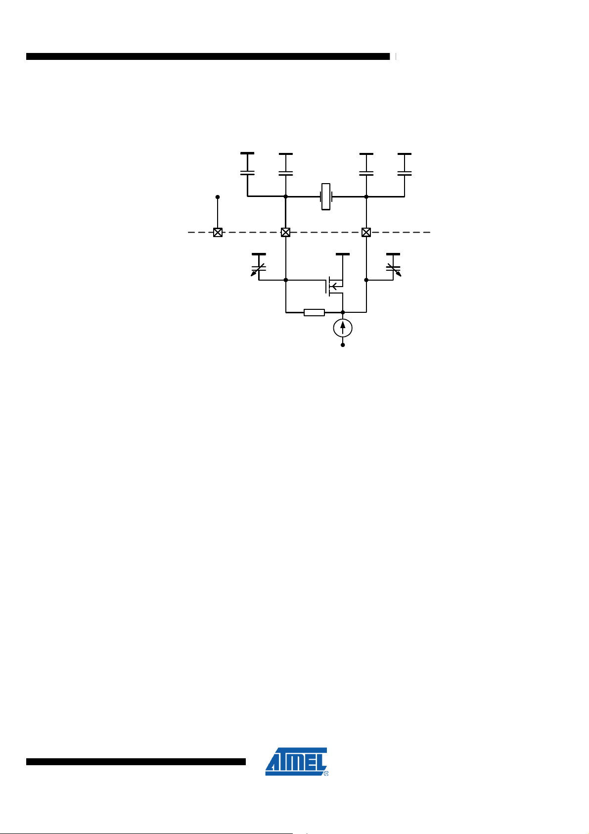
ATmega128RFA1
The following figure shows all parasitic capacitances, such as PCB stray capacitances
and the pin input capacitance summarized to C
Figure 9-25. Simplified XOSC Schematic with External Components
PAR
.
C
PAR
V
EVDD
EVDD
C
TRIM
XTAL_TRIM[3:0]
Additional internal trimming capacitors C
0 pF to 4.5 pF with a 0.3 pF resolution is selectable using XTAL_TRIM of register
XOSC_CTRL. To calculate the total load capacitance, the following formula can be
used
CL = 0.5 • (CX + C
The trimming capacitors provide the possibility to reduce frequency deviations caused
by variations of the production process or by tolerances of external components. Note
that the oscillation frequency can only be reduced by increasing the trimming
capacitance. The frequency deviation caused by one step of C
increasing values of the crystal load capacitor.
CX CX
16MHz
EVDD
are available. Any value in the range from
TRIM
TRIM
+ C
PAR
).
C
PAR
XTAL2XTAL1
XTAL_TRIM[3:0]
PCB
IC internal
C
TRIM
decreases with
TRIM
An amplitude control circuit is included to ensure stable operation under different
operating conditions and for different crystal types. Enabling the crystal oscillator after
leaving SLEEP state causes a slightly higher current during the amplitude build-up
phase to guarantee a short start-up time. The current is reduced to the amount
necessary for a robust oscillation during stable operation. This also keeps the drive
level of the crystal low.
Crystals with a higher load capacitance are generally less sensitive to parasitic pulling
effects caused by variations of external components or board and circuit parasitics. On
the other hand a larger crystal load capacitance results in a longer start-up time and a
higher steady state current consumption.
9.6.5.3 External Reference Frequency Setup
When using an external reference frequency, the signal must be connected to
pin XTAL1 as indicated in Figure 9-26 on page 82 and the bits XTAL_MODE of register
XOSC_CTRL need to be set to the external oscillator mode. The oscillation peak-topeak amplitude shall between 100 mV and 500 mV, the optimum range is between
400 mV and 500 mV. Pin XTAL2 should not be wired
8266A-MCU Wireless-12/09
81
Page 82

ATmega128RFA1
Figure 9-26. Setup for Using an External Frequency Reference
16 MHz
9.6.6 Frequency Synthesizer (PLL)
The main features of the phase-locked loop are:
• Generate RX/TX frequencies for all 2.4 GHz channels of IEEE 802.15.4;
• Autonomous calibration loops for stable operation within the operating range;
• Two PLL-interrupts for status indication;
• Fast PLL settling to support frequency hopping;
9.6.6.1 Overview
The PLL generates the RF frequencies for the radio transceiver. During receive
operation the frequency synthesizer works as a local oscillator for the receive frequency
of the radio transceiver. During transmit operation the voltage-controlled oscillator
(VCO) is directly modulated to generate the RF transmit signal. The frequency
synthesizer is implemented as a fractional-N PLL.
Two calibration loops ensure correct PLL functionality within the specified operating
limits.
9.6.6.2 RF Channel Selection
The PLL is designed to support 16 channels in the 2.4 GHz ISM band with channel
spacing of 5 MHz according to IEEE 802.15.4. The center frequency of these channels
is defined as follows:
XTAL1
XTAL2
PCB
IC internal
9.6.6.3 Frequency Agility
82
Fc = 2405 + 5 (k – 11) in [MHz], for k = 11, 12 ... 26
where k is the channel number.
The channel k is selected by the CHANNEL bits of register PHY_CC_CA.
When the PLL is enabled during state transition from TRX_OFF to PLL_ON the settling
time is typically t
(AVREG) and the PLL self calibration (refer to Table 9-8 on page 42Table 9-8 and ? ?
? ? ? ? ? ? ? ? ? ). A lock of the PLL is indicated with a TRX24_PLL_LOCK interrupt.
Switching between 2.4 GHz ISM band channels in PLL_ON or RX_ON states is
typically done within t
frequency hopping applications.
The PLL frequency is changed to the transmit frequency within t
starting the transmit procedure and before starting the transmission. After the
transmission the PLL settles back to the receive frequency within t
frequency step does not generate a TRX24_PLL_LOCK or TRX24_PLL_UNLOCK
interrupt within these time spans.
= 110 µs including the settling time of the analog voltage regulator
TR4
= 11 µs. This makes the radio transceiver highly suitable for
TR20
= 16 µs after
TR23
= 32 µs. This
TR24
8266A-MCU Wireless-12/09
Page 83

ATmega128RFA1
9.6.6.4 Calibration Loops
Due to temperature, supply voltage and part-to-part variations of the radio transceiver
the VCO characteristics diverge. Two automated control loops are implemented to
ensure a stable operation: center frequency (CF) tuning and delay cell (DCU)
calibration. Both calibration loops are initiated automatically when the PLL is enabled
during state transition from TRX_OFF to PLL_ON. The center frequency calibration is
additionally initiated when the PLL changes to a center frequency of another channel.
9.6.6.5 Interrupt Handling
It is recommended to initiate the calibration loops manually if the PLL operates for a
long time on the same channel e.g. more than 5 min or the operating temperature
changes significantly. Both calibration loops can be initiated manually by setting
PLL_CF_START = 1 of register PLL_CF and PLL_DCU_START = 1 of register
PLL_DCU. The device must be in PLL_ON or RX_ON state to start the calibration. The
completion of the center frequency tuning is indicated by a TRX24_PLL_LOCK
interrupt.
Both calibration loops may be run simultaneously.
Two different interrupts indicate the PLL status. The TRX24_PLL_LOCK interrupt
indicates that the PLL has locked. The TRX24_PLL_UNLOCK interrupt indicates an
unexpected unlock condition.
A TRX24_PLL_LOCK interrupt is supposed to occur in the following situations:
• State change from TRX_OFF to PLL_ON / RX_ON/ RX_AACK_ON/
TX_ARET_ON;
• Channel change in states PLL_ON / RX_ON/ RX_AACK_ON/ TX_ARET_ON;
Any other occurrences of PLL interrupts indicate erroneous behavior and require
checking of the actual device status.
The state transition from BUSY_TX to PLL_ON after successful transmission does not
generate a TRX24_PLL_LOCK interrupt within the settling period.
9.6.7 Automatic Filter Tuning (FTN)
The FTN is incorporated to compensate device tolerances for temperature, supply
voltage variations as well as part-to-part variations of the radio transceiver. The filtertuning result is used to correct the transfer function of the analog baseband filter and
the time constant of the PLL loop-filter (refer to "General Circuit Description" on page
30).
An FTN calibration cycle is initiated automatically when entering the radio transceiver
TRX_OFF state from the SLEEP or RESET state.
Although receiver and transmitter are very robust against these variations, it is
recommended to initiate the FTN manually if the radio transceiver does not use the
SLEEP state. A calibration cycle is to be initiated in states TRX_OFF, PLL_ON or
RX_ON if necessary. This applies in particular to the High Data Rate Modes with a
much higher sensitivity to variations of the BPF transfer function. The recommended
calibration interval is 5 min or less.
9.7 Radio Transceiver Usage
This section describes the basic procedures to receive and transmit frames with the
radio transceiver.
8266A-MCU Wireless-12/09
83
Page 84

ATmega128RFA1
9.7.1 Frame Receive Procedure
A frame reception comprises of two actions: The PHY listens for a frame, receives and
demodulates the frame to the Frame Buffer and signalizes its reception to the
application software. The application software reads the available frame data from the
Frame Buffer after or during the progress of the frame reception.
While in state RX_ON or RX_AACK_ON the radio transceiver searches for incoming
frames on the selected channel. First a TRX24_RX_START interrupt indicates the
detection of an IEEE 802.15.4 compliant frame assuming the appropriate interrupts are
enabled. The frame reception is completed when issuing the TRX24_RX_END
interrupt.
Different Frame Buffer read access scenarios are recommended for:
• Non-time critical applications: read access starts after the TRX24_RX_END interrupt;
• Time-critical applications: read access starts after the TRX24_RX_START interrupt;
The controller must ensure to read valid Frame Buffer contents. Reading frame data
before frame reception is finished can lead to invalid data, if buffer regions are
accessed which are not yet updated with the new frame.
While receiving a frame the data needs to be primarily stored in the Frame Buffer
before reading it. This is ensured by accessing the first Frame Buffer byte at least 32 µs
after the TRX24_RX_START interrupt.
9.7.2 Frame Transmit Procedure
It is recommended for operations considered to be not time-critical to wait for the
TRX24_RX_END interrupt before starting a Frame Buffer read access. The following
figure illustrates the frame receive procedure using the TRX24_RX_END interrupt.
Figure 9-27. Transactions between radio transceiver and microcontroller during receive
Transceiver
Critical protocol timing could require starting the Frame Buffer read access after the
TRX24_RX_START interrupt. The first byte of the frame data can be read 32 µs after
the TRX24_RX_START interrupt. The application software must ensure to read slower
than the frame is received. Otherwise a Frame Buffer under-run occurs and the frame
data may be not valid.
IRQ issued (RX_START)
IRQ issued (RX _END)
Read TST_FRAME_LENGTH register
(Register access)
Read frame data (Frame Buffer access)
Microcontroller
84
A frame transmission comprises of the two actions Frame Buffer write access and
transmission of the Frame Buffer content. Both actions can be run in parallel if required
by critical protocol timing.
Figure 9-28 on page 85 illustrates the frame transmit procedure by consecutively writing
and transmitting the frame. The frame transmission is initiated writing SLPTR or writing
8266A-MCU Wireless-12/09
Page 85

ATmega128RFA1
command TX_START to register TRX_STATE after a Frame Buffer write access and
while the radio transceiver is in state PLL_ON or TX_ARET_ON. The TRX24_TX_END
interrupt indicates the completion of the transaction.
Figure 9-28. Transaction between radio transceiver and microcontroller during transmit
Write frame data (Frame Buffer access)
Write TRX_CMD = TX_START, or write SLPTR
(Register access)
Transceiver
IRQ issued (TX_END)
Alternatively a frame transmission can be started first, followed by the Frame Buffer
write access (PSDU data) as shown in Figure 9-29 below. This is applicable for time
critical applications.
A transmission is initiated either by writing SLPTR or by writing the TX_START
command to the TRX_CMD bits of register TRX_STATE. The radio transceiver then
starts transmitting the SHR which is internally generated.
This first phase requires 16 µs for PLL settling and 160 µs for SHR transmission. The
PHR must be available in the Frame Buffer before this time elapses. Furthermore the
Frame Buffer must be filled faster than the frame is transmitted to prevent a buffer
under-run.
Figure 9-29. Time Optimized Frame Transmit Procedure
Write TRX_CMD = TX_START, or write SLPTR
(Register access)
Microcontroller
Write frame data (Frame Buffer access)
Transceiver
9.8 Radio Transceiver Extended Feature Set
9.8.1 Random Number Generator
The radio transceiver incorporates a 2-bit, noise observing, true random number
generator to be used to:
• Generate random seeds for CSMA-CA algorithm (see"Extended Operating Mode" on
page 43);
8266A-MCU Wireless-12/09
Microcontroller
IRQ issued (TX_END)
85
Page 86

ATmega128RFA1
9.8.2 High Data Rate Modes
• Generate random values for AES key generation (see
page 92);
The random number is updated every t
states. The values are stored in bits RND_VALUE of register PHY_RSSI.
The main features of the High Data Rate Modes are:
= 1 µs in Basic Operation Mode receive
TR29
"Security Module (AES)" on
9.8.2.1 Overview
• High Data Rate Communication up to 2 Mb/s;
• Support of Basic and Extended Operating Mode;
• Support of other features of the Extended Feature Set;
The radio transceiver also supports alternative data rates higher than 250 kb/s for
applications beyond IEEE 802.15.4 compliant networks.
The selection of a data rate does not affect the remaining functionality. Thus it is
possible to run all features and operating modes of the radio transceiver in various
combinations.
The data rate can be selected by writing bits OQPSK_DATA_RATE of register
TRX_CTRL_2.
The High Data Rate Modes occupy the same RF channel bandwidth as the
IEEE 802.15.4 – 2.4 GHz 250 kb/s standard mode. The sensitivity of the receiver is
reduced due to the decreased spreading factor. The following table shows typical
values of the sensitivity for different data rates.
Table 9-23. High Data Rate Sensitivity
High Data Rate Sensitivity Comment
250 kb/s -100 dBm PER ≤ 1%, PSDU length of 20 octets
500 kb/s -9 dBm PER ≤ 1%, PSDU length of 20 octets
1000 kb/s -9 dBm PER ≤ 1%, PSDU length of 20 octets
2000 kb/s -8 dBm PER ≤ 1%, PSDU length of 20 octets
By default there is no header based signaling of the data rate within a transmitted
frame. Thus nodes using a data rate other than the default IEEE 802.15.4 data rate of
250 kb/s are to be consistently configured in advance. The configurable start of frame
delimiter (SFD) could be alternatively used as an indicator of the PHY data rate (see
"Configurable Start-Of-Frame Delimiter (SFD)" on page 91).
9.8.2.2 High Data Rate Packet Structure
Higher data rate modulation is restricted to only the payload octets in order to allow
appropriate frame synchronization. The SHR and the PHR field are transmitted with the
IEEE 802.15.4 compliant data rate of 250 kb/s (refer to "Introduction – IEEE 802.15.4-
2006 Frame Format" on page 61).
A comparison of the general packet structure for different data rates with an example
PSDU length of 80 octets is shown in Figure 9-30 on page 87.
86
8266A-MCU Wireless-12/09
Page 87

ATmega128RFA1
Figure 9-30. High Data Rate Frame Structure
0 tim e [µs]192
512
832 147 2 2752
250 kb /s
500 kb /s
100 0 k b/s
200 0 k b/s
PSD U: 80 octets
SFD
PHR
PSD U: 80 octets
SFD
PHR
PSD U: 80 octets
SFD
PHR
PSD U: 80 octets
SFD
PHR
FCS
FCS
The effective data rate is smaller than the selected data rate due to the overhead
caused by the SHR, the PHR and the FCS. The overhead depends further on the
length of the PSDU. A graphical representation of the effective data rate is shown in the
2000
1000
500
250
2000 kbps
1000 kbps
500 kbps
250 kbps
following figure:
Figure 9-31. Effective Data Rate “B” for High Data Rate Mode
1600
1400
1200
1000
800
B [kbps]
600
400
200
0
0 20 40 60 80 100 120
Therefore High Data Rate transmission and reception is useful for large PSDU lengths
due to the higher effective data rate or to reduce the power consumption of the system.
Furthermore the active on-air time using High Data Rate Modes is significantly reduced.
9.8.2.3 High Data Rate Frame Buffer Access
The Frame Buffer access to read or write frames for High Data Rate communication is
similar to the procedure described in "Frame Buffer" on page 77. However the last byte
in the Frame Buffer after the PSDU data is the ED value rather than the LQI value.
9.8.2.4 High Data Rate Energy Detection
According to IEEE 802.15.4 the ED measurement duration is 8 symbol periods. For
frames operated at higher data rates the automated ED measurement duration is
reduced to 32 µs to take the reduced frame length into account ("Energy Detection
(ED)" on page 68).
8266A-MCU Wireless-12/09
PSDU length in octets
87
Page 88

ATmega128RFA1
9.8.2.5 High Data Rate Mode Options
Receiver Sensitivity Control
The different data rates between PPDU header (SHR and PHR) and PHY payload
(PSDU) cause a different sensitivity between header and payload. This can be adjusted
by defining sensitivity threshold levels of the receiver. The receiver does not receive
frames with an RSSI level below the defined sensitivity threshold level (register bits
RX_PDT_LEVEL > 0). Under these operating conditions the receiver current
consumption is reduced by 500 µA (refer to chapter
Specifications" on page 509).
A description of the settings to control the sensitivity threshold with register RX_SYN
can be found in section "RX_SYN – Transceiver Receiver Sensitivity Control Register"
on page 118.
"Current Consumption
Reduced Acknowledgment Timing
On higher data rates the IEEE 802.15.4 compliant acknowledgment frame response
time of 192 µs significantly reduces the effective data rate of the network. To minimize
this influence in Extended Operating Mode RX_AACK (see section "RX_AACK_ON –
Receive with Automatic ACK" on page 46), the acknowledgment frame response time
can be reduced to 32 µs. Figure 9-32 below illustrates an example for a reception and
acknowledgement of a frame with a data rate of 2000 kb/s and a PSDU length of 80
symbols. The PSDU length of the acknowledgment frame is 5 octets according to
IEEE 802.15.4.
Figure 9-32. High Data Rate AACK Timing
0
AA CK _A CK _TIM E = 0 P SDU : 80 o ctets
AA CK _A CK _TIM E = 1
PSD U: 80 oc tets
192 512
SFD
PHR
SFD
PHR
The acknowledgment time is reduced from 192 µs to 32 µs if bit AACK_ACK_TIME of
register XAH_CTRL_1 is set.
544
192 µ s
32 µs
704 91 6
AC K
SFD
PHR
tim e [µ s]
AC K
SFD
PHR
9.8.3 Antenna Diversity
9.8.3.1 Overview
88
The main features of the Antenna Diversity implementation are:
• Improves signal path robustness between nodes;
• Self-contained antenna diversity algorithm of the radio transceiver;
• Direct register based antenna selection;
The receive signal strength may vary and affect the link quality even for small changes
of the antenna location due to multipath propagation effects between network nodes.
These fading effects can result in an increased error floor or loss of the connection
between devices.
Antenna Diversity can be applied to reduce the effects of multipath propagation and
fading hence improving the reliability of a RF connection between network nodes.
8266A-MCU Wireless-12/09
Page 89

ATmega128RFA1
Antenna Diversity uses two antennas to switch to the most reliable RF signal path. This
is done by the radio transceiver during RX_LISTEN and RX_AACK_ON state without
interaction of the application software. Both antennas should be carefully separated
from each other to ensure highly independent receive signals.
Antenna Diversity can be used in Basic and Extended Operating Modes and can also
be combined with other features and operating modes like High Data Rate Mode and
RX/TX Indication.
9.8.3.2 Antenna Diversity Application Example
A block diagram for an application using an antenna switch is shown in the following
figure.
Figure 9-33. External Antenna Diversity – Block Diagram
AN T 0
AN T 1
Generally, the Antenna Diversity algorithm is enabled with bit ANT_DIV_EN=1 in
register ANT_DIV. For the External Antenna Diversity the control of the antenna switch
(SW1) must be enabled by bit ANT_EXT_SW_EN of register ANT_DIV. Under this
condition the control pins DIG1 and DIG2 are configured as outputs. DIG1 and DIG2
are used to feed the antenna switch signal and its inverse to the differential inputs of the
RF Switch (SW1).
The selected antenna is indicated by bit ANT_SEL of register ANT_DIV. The antenna
selection continues searching for new frames on both antennas after the frame
reception is completed. However the register bit ANT_SEL maintains its previous value
(from the last received frame) until a new SHR has been found and the selection
algorithm locked into one antenna again. Then the register bit ANT_SEL is updated.
The antenna defined by the ANT_CTRL bits of register ANT_DIV is selected for
transmission. If for example the same antenna as selected for reception is to be used
for transmission, the antenna must be set using the ANT_CTRL bits based on the value
read from the ANT_SEL bit. It is recommended to read bit ANT_SEL after the
TRX24_RX_START interrupt.
1
DIG2
2
DIG4
...
B1SW 1
RF-
Switch
Balun
10
7
8
9
AV S S
R F P
R F N
AV S S
...
AT m eg a1 28R F A 1
DIG3
DIG1
14 1 5
8266A-MCU Wireless-12/09
The autonomous search and selection allows the use of Antenna Diversity during
reception even if the application software currently does not control the radio
transceiver for instance in Extended Operating Mode.
An application software defined selection of a certain antenna can be done by disabling
the automatic Antenna Diversity algorithm (ANT_DIV_EN = 0) and selecting one
antenna using register bit ANT_CTRL.
89
Page 90

ATmega128RFA1
If the radio transceiver is not in a receive or transmit state, it is recommended to disable
register bit ANT_EXT_SW_EN and to set the port pins DIG1 and DIG2 to output low
(DDG1 = 1, PORTG1 = 0, DDF2 = 1, PORTF2 = 0) in order to reduce the power
consumption or avoid leakage current of the external RF switch especially during sleep
modes.
9.8.3.3 Antenna Diversity with Extended Operation Modes
A combination of Extended Operation Mode and antenna diversity is allowed.
While the radio transceiver is in RX_AACK_ON state, it switches to an antenna with a
reliable signal. The receive antenna selection is also used for transmission of an
automatic acknowledge frame.
While the radio transceiver is in TX_ARET state, the selected antenna is automatically
changed for every frame transmission retry.
9.8.3.4 Antenna Diversity Sensitivity Control
The detection threshold of the receiver has to be adjusted due to a different receive
algorithm used by the Antenna Diversity algorithm. It is recommended to set bits
PDT_THRES of register RX_CTRL to 3.
9.8.4 RX/TX Indicator
The main features are:
• RX/TX Indicator to control an external RF Front-End;
• Application software independent RF Front-End Control;
• Provide TX Timing Information;
9.8.4.1 Overview
While IEEE 802.15.4 is a low-cost, low-power standard, solutions supporting higher
transmit output power are occasionally desirable. A differential control pin pair can
indicate that the radio transceiver is currently in transmit mode to simplify the control of
an optional external RF front-end.
The control of an external RF front-end is done via the digital control pins DIG3/DIG4.
The function of this pin pair is enabled with bit PA_EXT_EN of register TRX_CTRL_1.
Pin DIG3 is set to low level and DIG4 to high level
The two pins change the polarity when the radio transceiver starts transmitting. This
differential pin pair can be used to control PA, LNA and RF switches.
If the radio transceiver is not in a receive or transmit state, it is recommended to disable
register bit PA_EXT_EN and to set the port pins DIG3 and DIG4 to output low (DDG0 =
1, PORTG0 = 0, DDF3 = 1, PORTF3 = 0) in order to reduce the power consumption or
avoid leakage current of external RF switches and other building blocks especially
during sleep modes.
9.8.4.2 External RF-Front End Control
The setup time of the external power amplifier (PA) relative to the internal building
blocks should be adjusted when using an external RF front-end including a power
amplifier to optimize the overall power spectral density (PSD) mask.
90
while the transmitter is turned off.
8266A-MCU Wireless-12/09
Page 91
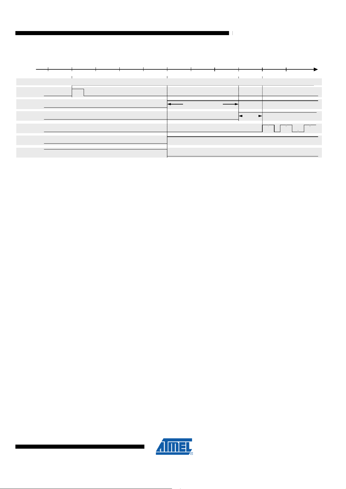
ATmega128RFA1
Figure 9-34. TX Power Ramping Control for RF Front-Ends
0 6 8 10
2 1 2 14 16 18
4
Le ng th [µ s]
TR X _ STA T E
SL P TR
PA bu ffer
PA
Mod ulatio n 1 1 1 1 1 10 00
DI G 3
DI G 4
PL L _O N
BU SY_ T X
PA _ BUF_ LT
PA_LT
The start-up sequence of the individual building blocks of the internal transmitter is
shown in the previous figure. The transmission is actually initiated by writing ‘1’ to
SLPTR. The radio transceiver state changes from PLL_ON to BUSY_TX and the PLL
settles to the transmit frequency within 16 µs (parameter tTR23 at page 42). The
modulation starts 16 µs (parameter tTR10 at page 42) after the SLPTR=1. The PA
buffer and the internal PA are enabled during this time.
The control of an external PA is done via the differential pin pair DIG3 and DIG4.
DIG3 = H / DIG4 = L indicates that the transmission starts and can be used to enable
an external PA. The timing of pins DIG3/DIG4 can be adjusted relative to the start of the
frame and the activation of the internal PA buffer. This is controlled using the register
bits PA_BUF_LT and PA_LT. For details refer to Figure 9-22 on page 77.
9.8.5 RX Frame Time Stamping
To determine the exact timing of an incoming frame e.g. for beaconing networks, the
Symbol Counter should be used. SFD Time Stamping is enabled by setting bit SCTSE
of the Symbol Counter Control Register SCCR0. The actual 32 Bit Symbol Counter
value is captured in the SFD Time Stamp register SCTSR at the time, the SFD has
been received. For details see section "SFD and Beacon Timestamp Generation" on
page 135.
9.8.6 Configurable Start-Of-Frame Delimiter (SFD)
The SFD is a field indicating the end of the SHR and the start of the packet data. The
length of the SFD is 1 octet (2 symbols). This octet is used for byte synchronization only
and is not included in the Frame Buffer.
The value of the SFD could be changed if it is needed to operate non IEEE 802.15.4
compliant networks. An IEEE 802.15.4 compliant network node does not synchronize to
frames with a different SFD value.
The register SFD_VALUE contains the one octet start-of-frame delimiter (SFD) to
synchronize to a received frame. It is not recommended to set the low-order 4 bits to 0
due to the way the SHR is formed.
9.8.7 Dynamic Frame Buffer Protection
The ATmega128RFA1 continues the reception of incoming frames as long as it is in
any receive state. When a frame was successfully received and stored into the Frame
Buffer, the following frame will overwrite the Frame Buffer content again. To relax the
timing requirements for a Frame Buffer read access the Dynamic Frame Buffer
8266A-MCU Wireless-12/09
91
Page 92

ATmega128RFA1
Protection prevents that a new valid frame passes to the Frame Buffer until the buffer
protection bit is cleared (RX_SAFE_MODE = 0).
A received frame is automatically protected against overwriting:
• in Basic Operating Mode, if its FCS is valid
• in Extended Operating Mode, if an TRX24_RX_END interrupt is generated
The Dynamic Frame Buffer Protection is enabled, if register bit RX_SAFE_MODE
(register TRX_CTRL_2, see
112) is set and the radio transceiver state is RX_ON or RX_AACK_ON.
Note that Dynamic Frame Buffer Protection only prevents write accesses from the air
interface not from the application software. The application software may still modify the
Frame Buffer content.
"TRX_CTRL_2 – Transceiver Control Register 2" on page
9.8.8 Security Module (AES)
The security module (AES) is characterized by:
• Hardware accelerated encryption and decryption;
• Compatible with AES-128 standard (128 bit key and data block size);
• ECB (encryption/decryption) mode and CBC (encryption) mode support;
• Stand-alone operation, independent of other blocks;
See TBD Application regarding the AES security module usage.
9.8.8.1 Overview
The security module is based on an AES-128 core according to the FIPS197 standard
[5]. and provides two modes, the Electronic Code Book (ECB) and the Cipher Block
Chaining (CBC). The security module works independent of other building blocks of the
radio transceiver. Encryption and decryption can be performed in parallel to a frame
transmission or reception.
The ECB and CBC modules including the AES core are clocked with the 16 MHz Radio
Transceiver Crystal Oscillator.
Controlling the security block is possible over 5 Registers within AVR I/O space:
Table 9-24. Security Module Address Space Overview
9.8.8.2 Security Module Preparation
Register Name Description
AES_STATUS AES status register
AES_CTRL AES control register
AES_KEY Access to 16 Byte key buffer
AES_STATE Access to 16 Byte data buffer
92
The use of the security module requires a configuration of the security engine before
starting a security operation. The following steps are required:
Table 9-25. AES Engine Configuration Steps
Step Description Description
1 Key Setup Write encryption or decryption key to KEY
buffer
(16 consecutive byte writes to AES_KEY)
8266A-MCU Wireless-12/09
Page 93

ATmega128RFA1
Step Description Description
2 AES configuration Select AES mode: ECB or CBC
Select encryption or decryption
Enable the AES Encryption Ready Interrupt
AES_READY
3 Write Data Write plaintext or cipher text to DATA buffer
(16 consecutive byte writes to AES_STATE)
4 Start operation Start AES operation
5 Wait for AES finished:
1. AES_READY IRQ or
2. polling AES_DONE bit
(register AES_STATUS) or
3. wait for 24 µs
6 Read Data Read cipher text or plaintext from DATA buffer
Before starting any security operation a 16 Byte key must be written to the security
engine (refer to section "Security Key Setup" below). This can be done by 16
consecutive write accesses to the I/O register AES_KEY. An internal address counter is
incremented automatically with every read/ write operation. An AES encryption/
decryption run resets the internal byte counter. If the key and data buffer has not been
read or written completely (all 16 Bytes), the following encryption/ decryption operation
will finish with an error.
Wait until AES encryption/decryption is
finished successfully
(16 consecutive byte reads from AES_STATE)
9.8.8.3 Security Key Setup
The following step selects either Electronic Code Book (ECB) or Cipher Block Chaining
(CBC) as the AES_MODE. These modes are explained in more detail in section
"Security Operation Modes" on page 94. Encryption or decryption must be further
selected with bit AES_DIR of register AES_CTRL.
If the AES Error or AES Ready IRQ is used, the interrupt must be enabled with bit
AES_IM.
Next the 128-bit plain text or cipher text data has to be provided to the AES hardware
engine. The 16 data bytes must be consecutively written to the AES_STATE register.
The AES_STATE register can be accessed in the same way as the key register (refer to
"Security Key Setup" below).
The encryption or decryption is initiated with bit AES_REQUEST = 1.
The operation takes 24 µs and the completed encryption/ decryption is indicated by the
AES_READY IRQ and the AES_DONE bit. The internal byte counter of the key and
data buffer is cleared and the resulting data can be read out.
For additional information about the key and data buffer please refer to section
"AES_KEY – AES Encryption and Decryption Key Buffer Register" on page 102 and
"AES_STATE – AES Plain and Cipher Text Buffer Register" on page 102.
Notes: 1. Access to the security block is not possible while the radio transceiver is in state
SLEEP.
2. All configurations of the security module, the SRAM content and keys are reset
during SLEEP or RESET states.
8266A-MCU Wireless-12/09
The key is stored in a 16 Byte sequential buffer. To read or write the contents of the
buffer, 16 consecutive read or write operations to the AES_KEY register are required.
93
Page 94
ATmega128RFA1
A 16-folded read access to registers AES_KEY returns the last round key of the
preceding security operation. This is the key required for the corresponding ECB
decryption operation after an ECB encryption operation. However the initial AES key
written to the security module in advance of an AES run (see step 1 in
page 92) is not modified during an AES operation. This initial key is used for the next
AES run although it cannot be read from AES_KEY.
Before accessing the Key Buffer it must be ensured, that the internal address counter is
initialized correctly. This is the cases after Radio Transceiver Reset (see TRXPR –
Transceiver Pin Register on page 169) or a completed AES Encryption/ Decryption
operation. After an interrupted buffer read or write access, Address pointer
reinitialization is recommended by a simple read access to the AES_CTRL register.
Note: 1. ECB decryption is not required for IEEE 802.15.4 or ZigBee security processing.
9.8.8.4 Security Operation Modes
9.8.8.4.1 Electronic Code Book (ECB)
ECB is the basic operating mode of the security module and is configured by the
AES_CTRL register. The bit AES_MODE = 0 defines the ECB mode and bit AES_DIR
selects the direction to either encryption or decryption. The data to be processed has to
be written to registers AES_STATE.
A security operation can be started by writing the start command AES_REQUEST = 1
(AES_CTRL register).
Table 9-25 on
The radio transceiver provides this functionality as an additional feature.
The ECB encryption operation is illustrated in Figure 9-35 below. Figure 9-36 below
shows the ECB decryption mode which is supported in a similar way.
Figure 9-35. ECB Mode - Encryption
Plaintext
Encryption
Key
Figure 9-36. ECB Mode - Decryption
Decryption
Key
Block Cipher
Encryption
Ciphertext
Ciphertext
Block Cipher
Decryption
Encryption
Key
Decryption
Key
Plaintext
Block Cipher
Encryption
Ciphertext
Ciphertext
Block Cipher
Decryption
94
Plaintext
Due to the nature of AES algorithm the initial key to be used when decrypting is not the
same as the one used for encryption. Instead it is the last round key. This last round
Plaintext
8266A-MCU Wireless-12/09
Page 95
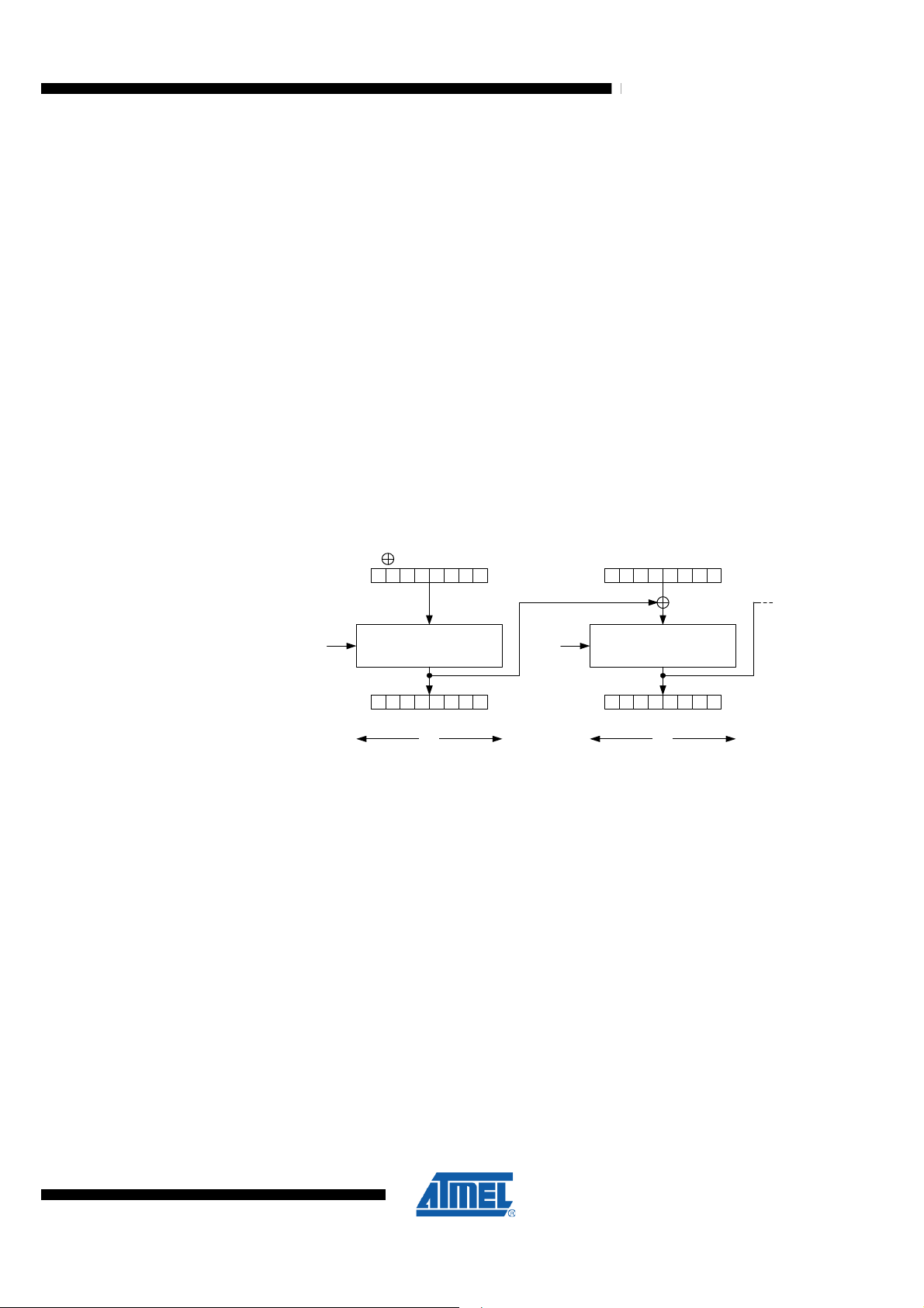
ATmega128RFA1
key is the content of the key address space stored after running one full encryption
cycle and must be saved for decryption. If the decryption key has not been saved, it has
to be recomputed by first running a dummy encryption (of an arbitrary plaintext) using
the original encryption key. Then the resulting round key must be fetched from the key
memory and written back into the key memory as the decryption key.
ECB decryption is not used by either IEEE 802.15.4 or ZigBee frame security. Both of
these standards do not directly encrypt the payload. Instead they protect the payload by
applying a XOR operation between the original payload and the resulting (AES-) cipher
text with a nonce (number used once). As the nonce is the same for encryption and
decryption only ECB encryption is required. Decryption is performed by a XOR
operation between the received cipher text and its own encryption result concluding in
the original plain text payload upon success.
9.8.8.4.2 Cipher Block Chaining (CBC)
In CBC mode the result of a previous AES operation is XOR-combined with the new
incoming vector forming the new plaintext to encrypt as shown in the next figure. This
mode is used for the computation of a cryptographic checksum (message integrity
code, MIC).
Figure 9-37. CBC Mode - Encryption
Plaintext Initialization Vector (IV)
Encryption
Key
Block Cipher
Encryption
Encryption
Key
Plaintext
Block Cipher
Encryption
Ciphertext
ECB
mode
After preparing the AES key and defining the AES operation direction register bit
AES_DIR, the data has to be provided to the AES engine and the CBC operation can
be started.
The first CBC run has to be configured as ECB to process the initial data (plain text
XOR with an initialization vector provided by the application software). All succeeding
AES runs are to be configured as CBC by setting bit AES_MODE = 1 (AES_CTRL
register ). Bit AES_DIR (AES_CTRL register) must be set to AES_DIR = 0 to enable
AES encryption. The data to be processed has to be transferred to the AES_STATE
register. Setting bit AES_REQUEST = 1 (AES_CTRL register) as described in section
"Security Operation Modes" on page 94 starts the first encryption. This causes the next
128 bits of plain text data to be XORed with the previous cipher text data, see Figure 9-
37 above.
Ciphertext
CBC
mode
8266A-MCU Wireless-12/09
According to IEEE 802.15.4 the input for the very first CBC operation has to be
prepared by a XOR operation of the plain text with the initialization vector (IV). The
value of the initialization vector is 0. However any other initialization vector can be
applied for non-compliant usage. This operation has to be prepared by the application
software.
Note that the MIC algorithm of the IEEE 802.15.4-2006 standard requires CBC mode
encryption only because it implements a one-way hash function.
95
Page 96

ATmega128RFA1
The status of the security processing is indicated by register AES_STATUS. After a
AES processing time of 24 µs the register bit AES_DONE changes to 1 (register
AES_STATUS) indicating that the security operation has finished (see
Timing Characteristics" on page 507).
The end of the AES processing can also be indicated by the AES_READY Interrupt.
The bit AES_ER of register AES_STATUS is set if the operation has finished with an
error. Otherwise this bit is zero but AES_DONE is ‘1’.
"Digital Interface
9.8.8.5 AES Interrupt Handling
The AES Interrupt handling is slightly different from all other IRQ’s. If the AES_IM Bit
(AES_CTRL Register) and the global interrupt enable flag is set, the AES core can
generate an AES Ready Interrupt (AES_READY). If the IRQ is issued, the
AES_STATUS register must be read to check the finish status of the last operation. If
AES_DONE is set, the last AES operation finished successfully. If AES_ER is set, an
error occurred during the last operation. The AES_ER flag is cleared automatically
during the read access to the AES_STATUS register. The AES_DONE flag is cleared
during the next read or write access to the AES_STATE (AES data) register.
The two status flags must be cleared before a new Interrupt can be issued.
If AES_IM is not set, the processing status can be polled by software (AES_STATUS
register), but no Interrupt occurs.
9.9 Continuous Transmission Test Mode
9.9.1 Overview
The 2.4GHz transceiver offers a Continuous Transmission Test Mode to support final
application / production tests as well as certification tests. In this test mode the radio
transceiver transmits continuously a previously transferred frame (PRBS mode) or a
continuous wave signal (CW mode).
In CW mode two different signal frequencies per channel can be transmitted:
9.9.2 Configuration
96
• f1 = fCH + 0.5 MHz
• f2 = fCH - 0.5 MHz
Here fCH is the channel center frequency programmed by register PHY_CC_CCA.
Note that in CW mode it is not possible to transmit a RF signal directly on the channel
center frequency. PSDU data in the Frame Buffer must contain at least a valid PHR
(see section "Introduction – IEEE 802.15.4-2006 Frame Format" on page 61). It is
recommended to use a frame of maximum length (127 bytes) and arbitrary PSDU data
for the PRBS mode. The SHR and the PHR are not transmitted. The transmission starts
with the PSDU data and is repeated continuously.
All register configurations shall be setup as follows before enabling Continuous
Transmission Test Mode:
• TX channel setting (optional);
• TX output power setting (optional);
• Mode selection (PRBS / CW);
An access to the registers TST_CTRL_DIGI and PART_NUM enables the Continuous
Transmission Test Mode.
8266A-MCU Wireless-12/09
Page 97

ATmega128RFA1
The transmission is started by enabling the PLL (TRX_CMD = PLL_ON) and writing the
TX_START command to register TRX_STATE.
Even for CW signal transmission it is required to write valid PSDU data to the Frame
Buffer. For PRBS mode it is recommended to write a frame of maximum length.
The detailed programming sequence is shown in Table 9-26 below. The column R/W
informs about writing (W) or reading (R) a register or the Frame Buffer.
Table 9-26. Continuous Transmission Programming Sequence
Step Action Register R/W Value Description
1 RESET Reset the transceiver
2 Register Access IRQ_MASK W 0x01 Set IRQ mask register, enable
3 Register Access TRX_CTRL_1 W 0x00 Disable TX_AUTO_CRC_ON
4 Register Access TRX_STATE W 0x03 Set radio transceiver state
5 Register Access PHY_CC_CCA W 0x33 Set IEEE 802.15.4 CHANNEL,
6 Register Access PHY_TX_PWR W 0x00 Set TX output power, e.g. to P
7 Register Access TRX_STATUS R 0x08 Verify TRX_OFF state
8 Register Access TST_CTRL_DIGI W 0x0F Enable Continuous Transmission
(1)
9
Register Access TRX_CTRL_2 W 0x03 Enable High Data Rate Mode, 2
(1)
10
Register Access RX_CTRL W 0xA7 Configure High Data Rate Mode
(2)
11
Frame Buffer
Write Access
12 Register Access PART_NUM W 0x54 Enable Continuous Transmission
13 Register Access PART_NUM W 0x46 Enable Continuous Transmission
14 Register Access TRX_STATE W 0x09 Enable PLL_ON state
15 Interrupt event R 0x01 Wait for PLL_LOCK interrupt
16 Register Access TRX_STATE W 0x02 Initiate Transmission,
17 Measurement Perform measurement
18 Register Access TRX_CTRL_2 W 0x00 Disable Continuous
19 RESET Reset the transceiver
Notes: 1. Only required for CW mode, do not configure for PRBS mode.
2. Frame Buffer content varies for different modulation schemes.
PLL_LOCK interrupt and set
global AVR IRQ enable
TRX_OFF
e.g. 19
Test Mode – step # 1
Mb/s
W Write PSDU data (even for CW
mode), refer to Table 9-27 on
page 98
Test Mode – step # 2
Test Mode – step # 3
enter BUSY_TX state
Transmission Test Mode
max
8266A-MCU Wireless-12/09
The content of the Frame Buffer has to be defined for Continuous Transmission PRBS
mode or CW mode. To measure the power spectral density (PSD) mask of the
transmitter it is recommended to use a random sequence of maximum length for the
PSDU data.
97
Page 98

ATmega128RFA1
9.10 Abbreviations
To measure CW signals it is necessary to write either 0x00 or 0xFF to the Frame
Buffer. For details refer to
Table 9-27. Frame Buffer Content for various Continuous Transmission Modulation
Schemes
Step Action Frame Content Comment
11 Frame Buffer
Write Access
Table 9-27 below.
Random Sequence modulated RF signal
0x00 (each byte) fCH – 0.5 MHz, CW signal
0xFF (each byte) fCH + 0.5 MHz, CW signal
AACK - Automatic acknowledgement
ACK - Acknowledgement
ADC - Analog-to-digital converter
AD - Antenna diversity
AGC - Automated gain control
AES - Advanced encryption standard
ARET - Automatic retransmission
AVREG - Voltage regulator for analog building blocks
AWGN - Additive White Gaussian Noise
BATMON - Battery monitor
BBP - Base band processor
BPF - Band pass filter
CBC - Cipher block chaining
CRC - Cyclic redundancy check
CCA - Clear channel assessment
CSMA-CA - Carrier sense multiple access/Collision avoidance
CW - Continuous wave
98
DVREG - Voltage regulator for digital building blocks
ECB - Electronic code book
ED - Energy detection
ESD - Electro static discharge
EVM - Error vector magnitude
FCF - Frame control field
FCS - Frame check sequence
FIFO - First in first out
FTN - Filter tuning network
GPIO - General purpose input output
8266A-MCU Wireless-12/09
Page 99

ATmega128RFA1
ISM - Industrial, scientific, and medical
LDO - Low-drop output
LNA - Low-noise amplifier
LO - Local oscillator
LQI - Link quality indicator
LSB - Least significant bit
MAC - Medium access control
MFR - MAC footer
MHR - MAC header
MSB - Most significant bit
MSDU - MAC service data unit
MPDU - MAC protocol data unit
MSK - Minimum shift keying
O-QPSK - Offset - quadrature phase shift keying
PA - Power amplifier
PAN - Personal area network
PCB - Printed circuit board
PER - Packet error rate
PHR - PHY header
PHY - Physical layer
PLL - Phase locked loop
POR - Power-on reset
PPF - Poly-phase filter
PRBS - Pseudo random bit sequence
PSDU - PHY service data unit
PSD - Power spectral mask
QFN - Quad flat no-lead package
RF - Radio frequency
RSSI - Received signal strength indicator
RX - Receiver
SFD - Start-of-frame delimiter
SHR - Synchronization header
SPI - Serial peripheral interface
8266A-MCU Wireless-12/09
SRAM - Static random access memory
SSBF - Single side band filter
TX - Transmitter
99
Page 100

ATmega128RFA1
9.11 Reference Documents
VCO - Voltage controlled oscillator
VREG - Voltage regulator
XOSC - Crystal oscillator
[1] IEEE Std 802.15.4™-2006: Wireless Medium Access Control (MAC) and
Physical Layer (PHY) Specifications for Low-Rate Wireless Personal Area
Networks (LR-WPANs)
[2] IEEE Std 802.15.4™-2003: Wireless Medium Access Control (MAC) and
Physical Layer (PHY) Specifications for Low-Rate Wireless Personal Area
Networks (LR-WPANs)
[3] ANSI / ESD-STM5.1-2001: ESD Association Standard Test Method for
electrostatic discharge sensitivity testing – Human Body Model (HBM).
[4] ESD-STM5.3.1-1999: ESD Association Standard Test Method for electrostatic
discharge sensitivity testing – Charged Device Model (CDM).
[5] NIST FIPS PUB 197: Advanced Encryption Standard (AES), Federal
Information Processing Standards Publication 197, US Department of
Commerce/NIST, November 26, 2001
[6] ATmega128RFA1 Software Programming Model
9.12 Register Description
9.12.1 AES_CTRL – AES Control Register
100
Bit 7 6 5 4 3 2 1 0
NA ($13C) AES_REQUEST
Read/Write RW R RW R RW RW R R
Initial Value
This register controls the operation of the security module. Do not access this register
during AES operation to read the AES core status. A read or write access to the register
stops the ongoing processing. To read the AES status use bit AES_DONE of register
AES_STATUS. Note that the AES_CTRL register is cleared when entering the radio
transceiver SLEEP state.
• Bit 7 – AES_REQUEST - Request AES Operation.
A write access with AES_REQUEST = 1 initiates the AES operation.
• Bit 6 – Res - Reserved Bit
This bit is reserved for future use. The result of a read access is undefined. The register
bit must always be written with the reset value.
• Bit 5 – AES_MODE - Set AES Operation Mode
This register bit sets the AES operation mode (ECB/CBC Mode).
0 0 0 0 0 0 0 0
Res AES_MODE Res AES_DIR AES_IM Res1 Res0 AES_CTRL
8266A-MCU Wireless-12/09
 Loading...