

Page 1

Features
• Utilizes the AVR
• AVR - High-performance and Low-power RISC Architecture
– 120/121 Powerful Instructions - Most Single Clock Cycle Execution
– 32 x 8 General Purpose Working Registers + Peripheral Control Registers
– Up to 6 MIPS Throughput at 6 MHz
• Data and Nonvolatile Program Memory
– 64K/128K Bytes of In-System Programmable Flash
Endurance: 1,000 Write/Erase Cycles
– 4K Bytes Internal SRAM
– 2K/4K Bytes of In-System Programmable EEPROM
Endurance: 100,000 Write/Erase Cycles
– Programming Lock for Flash Program and EEPROM Data Security
– SPI Interface for In-System Programming
• Peripheral Features
– On-chip Analog Comparator
– Programmable Watchdog Timer with On-chip Oscillator
– Programmable Serial UART
– Master/Slave SPI Serial Interface
– Real Time Counter (RTC) with Separate Oscillator
– Two 8-bit Timer/Counters with Separate Prescaler and PWM
– Expanded 16-bit Timer/Counter system, with Separate Prescaler,
Compare, Capture Modes and Dual 8-, 9-, or 10-bit PWM
– Programmable Watchdog Timer with On-chip Oscillator
– 8-channel, 10-bit ADC
• Special Microcontroller Features
– Low-power Idle, Power Save and Power Down Modes
– Software Selectable Clock Frequency
– External and Internal Interrupt Sources
• Specifications
– Low-power, High-speed CMOS Process Technology
– Fully Static Operation
• Power Consumption at 4 MHz, 3V, 25°C
– Active: 5.5 mA
– Idle Mode: 1.6 mA
– Power Down Mode: < 1 µA
• I/O and Packages
– 32 Programmable I/O Lines, 8 Output Lines, 8 Input Lines
– 64-pin TQFP
• Operating Voltages
– 2.7 - 3.6V (ATmega603L and ATmega103L)
– 4.0 - 5.5V (ATmega603 and ATmega103)
• Speed Grades
– 0 - 4 MHz (ATmega603L and ATmega103L)
– 0 - 6 MHz (ATmega603 and ATmega103)
®
RISC Architecture
8-bit
Microcontroller
with 64K/128K
Bytes In-System
Programmable
Flash
ATmega603
ATmega603L
ATmega103
ATmega103L
Preliminary
Rev. 0945D–06/99
1
Page 2
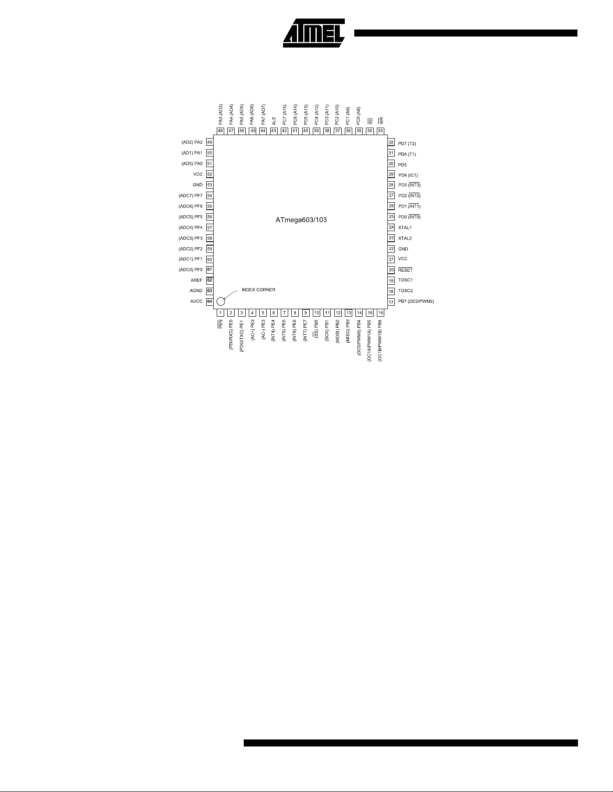
Pin Configuration
TQFP
Description
The ATmega603/103 is a low-power CM OS 8-bit microc ontroller based on the AVR RISC architectur e. By executing
powerful instructions in a single clock cycle, the ATmega603/103 achieves throughputs approaching 1 MIPS per MHz
allowing the system designer to optimize power consumption versus processing speed.
The AVR core is based on an enhanced RISC architecture that combines a rich instruction set wi th 32 general purpose
working registers. All the 32 registers are directly connected to the Arithmetic Logic Unit (ALU), allowing two independent
registers to be accessed in one single instruction executed in one clock cycle. The resulting architecture is more code
efficient while achieving throughputs up to ten times faster than conventional CISC microcontrollers.
The ATmega603/103 provides the following features: 64K/128K bytes of In-system Programmable Flash, 2K/4K bytes
EEPROM, 4K by tes S RAM, 32 g eneral pur pose I/O li nes, 8 In put l ines , 8 Ou tput l ines , 32 genera l pur pos e work ing registers, Real Time Counter (RTC), 4 flexible timer/counters with compare modes and PWM, UART, programmable Watchdog
Timer with internal oscillator, an SPI serial port and three software selectable power saving modes. The Idle Mode stops
the CPU while allowing the SRAM, timer/counters, SPI port and interrupt system to continue functioning. The Power Down
mode saves the register contents but freezes the oscillator, disabling all other chip functions until the next interrupt or hardware reset. In Power Sav e m ode , the tim er osci ll ato r con tin ues to ru n, al lo win g the us er to m ai ntai n a tim er base while the
rest of the device is sleeping.
The device is manu factured using At mel’s hig h-densi ty nonv olatile m emory technolog y. The on-c hip ISP Flas h allow s the
program memory to be reprogrammed in-system through a serial interface or by a conventional nonvolatile memory programmer. By combining an 8-bit RISC CPU with a large array of ISP Flash on a monolithic chip, the Atmel ATmega603/103
is a powerful mi crocontroller that provides a highly flex ible and cos t effective sol ution to many e mbedded contr ol
applications.
The ATmega603/103 AVR is supported with a full suite of program and system development tools including: C compilers,
macro assemblers, program debugger/simulators, in-circuit emulators, and evaluation kits.
2
ATmega603/103
Page 3
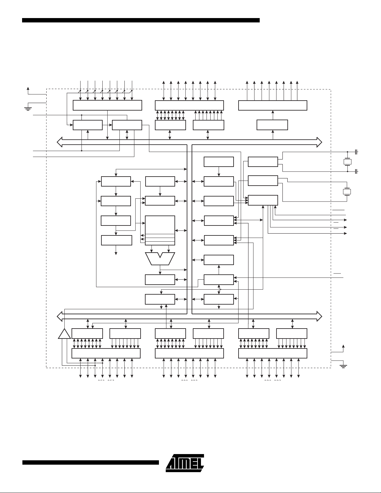
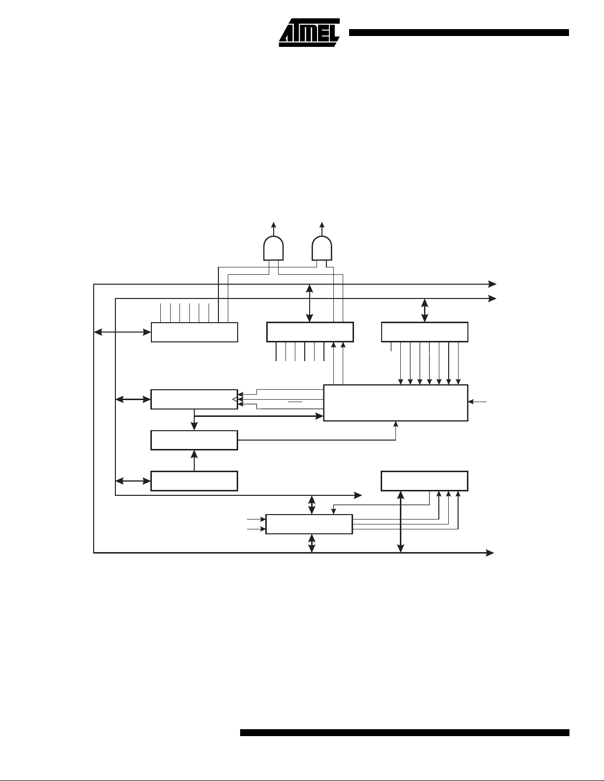
Block Diagram
Figure 1. The ATmega603/103 Block Diagram
VCC
GND
AVCC
PORTF BUFFERS
ANALOG MUX ADC
PORTA DRIVER/BUFFERS
DATA REGISTER
PORTA
DATA DIR.
REG. PORTA
8-BIT DATA BUS
ATmega603/103
PORTC DRIVERS
DATA REGISTER
PORTC
AGND
AREF
PROGRAM
COUNTER
PROGRAM
FLASH
INSTRUCTION
REGISTER
INSTRUCTION
DECODER
CONTROL
LINES
STACK
POINTER
SRAM
GENERAL
PURPOSE
REGISTERS
X
Y
Z
ALU
STATUS
REGISTER
SPI
INTERNAL
OSCILLATOR
WATCHDOG
TIMER
MCU CONTROL
REGISTER
TIMER/
COUNTERS
INTERRUPT
UNIT
EEPROM
PROGRAMMING
LOGIC
UART
OSCILLATOR
OSCILLATOR
TIMING AND
CONTROL
XTAL1
XTAL1
TOSC2
TOSC1
RESET
ALE
WR
RD
PEN
ANALOG
COMPARATOR
DATA REGISTER
+
-
PORTE
DATA DIR.
REG. PORTE
DATA REGISTER
PORTB
PORTB DRIVER/BUFFERSPORTE DRIVER/BUFFERS
DATA DIR.
REG. PORTB
DATA REGISTER
PORTD
PORTD DRIVER/BUFFERS
DATA DIR.
REG. PORTD
VCC
GND
3
Page 4

Comparison Between ATmega603 and ATmega103
The ATmega603 has 64K bytes of In-System Programmable Flash, 2K bytes of EEPROM, and 4K bytes of internal SRAM.
The ATmega603 does not have the ELPM instruction.
The ATmega103 has 128K bytes of In-System Programmable Flash, 4K bytes of EEPROM, and 4K bytes of internal
SRAM. The ATmega103 has the ELPM instruction, necessary to reach the upper half of the F lash memory for constant
table lookup.
Table 1 summarizes the different memory sizes for the two devices.
Table 1. Memory Size Summary
Part Flash EEPROM SRAM
ATmega603 64K bytes 2K bytes 4K bytes
ATmega103 128K bytes 4K bytes 4K bytes
Pin Descriptions
VCC
Supply voltage
GND
Ground
Port A (PA7..PA0)
Port A is an 8-bit bi-directional I/O port. Port pins can provide internal pull-up resistors (selected for each bit). The Port A
output buffers can si nk 20 mA and can dr ive LED disp lays direc tly. When pins PA 0 to PA7 are used as inputs and ar e
externally pulled low, they will source current if the internal pull-up resistors are activated.
Port A serves as Multiplexed Address/Data bus when using external SRAM.
The port A pins are tri-stated when a reset condition becomes active, even if the clock is not running.
Port B (PB7..PB0)
Port B is an 8-bi t bi -dir ec ti ona l I/O p or t wi th in ter nal pull-up resistors. The Po rt B ou tput bu ffer s can si nk 2 0 m A. A s inp uts ,
Port B pins that are externally pulled low, will source current if the pull-up resistors are activated.
Port B also serves the functions of various special features.
The port B pins are tri-stated when a reset condition becomes active, even if the clock is not running.
Port C (PC7..PC0)
Port C is an 8-bit Output port. The Port C output buffers can sink 20 mA.
Port C also serves as Address output when using external SRAM.
Since Port C is an output only port, the port C pins are not tri-stated when a reset condition becomes active.
Port D (PD7..PD0)
Port D is an 8-bit bi-di r ectio nal I/O port with internal pull-up resi st or s. The P or t D ou tput buff er s can si nk 20 m A. A s inp uts ,
Port D pins that are externally pulled low will source current if the pull-up resistors are activated.
Port D also serves the functions of various special features.
The port D pins are tri-stated when a reset condition becomes active, even if the clock is not running.
4
ATmega603/103
Page 5

ATmega603/103
Port E (PE7..PE0)
Port E is an 8-bi t bi - direc ti ona l I/O p or t wi th in ter nal p ull -up resistors. The Po rt E ou tput bu ffer s c an si nk 2 0 m A. A s inp uts,
Port E pins that are externally pulled low will source current if the pull-up resistors are activated.
Port E also serves the functions of various special features.
The port E pins are tri-stated when a reset condition becomes active, even if the clock is not running
Port F (PF7..PF0)
Port F is an 8-bit Input port. Port F also serves as the analog inputs for the ADC.
RESET
Reset input. An exter nal res et is gen erate d by a lo w le vel on the RESET pin. Res et p ul ses l on ger th an 5 0 n s w ill g ener a te
a reset, even if the clock is not running. Shorter pulses are not guaranteed to generate a reset.
XT AL1
Input to the inverting oscillator amplifier and input to the internal clock operating circuit.
XT AL2
Output from the inverting oscillator amplifier
TOSC1
Input to the inverting Timer/Counter oscillator amplifier
TOSC2
Output from the inverting Timer/Counter oscillator amplifier
WR
External SRAM Write Strobe.
RD
External SRAM Read Strobe.
ALE
ALE is the Address Latch Enable used when the Exter nal Memory is enabled. The ALE strobe is used to latc h the loworder address (8 bits) into an address latch during the first access cycle, and the AD0-7 pins are used for data during the
second access cycle.
AVCC
This is the supply voltage to the A /D Con verte r. It sho ul d be exter na lly c onn ec ted to V
for details on operation of the ADC.
AREF
This is the analog reference input for the ADC converter. For ADC operations, a voltage in the range AGND to AVCC must
be applied to this pin.
AGND
If the board has a separate ana log ground plane, this pin should be con nec ted to thi s gro und pla ne. Ot he rwis e, c onn ec t to
GND.
via a low-pass filter. See page 66
CC
PEN
This is a programming ena ble pin for the low-v oltage serial program ming mo de. By holdin g this pin low during a power -on
reset, the device will enter the serial programming mode. PEN
has no function during normal operation.
5
Page 6
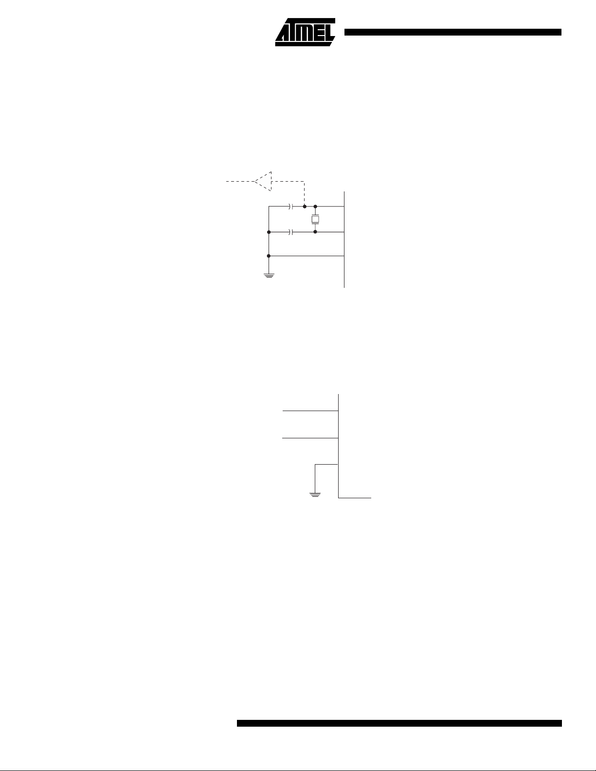
Clock Options
Crystal Oscillator
XTAL1 and XTAL2 are input and output, respectively, of an inverting amplifier which can be configured for use as an onchip oscillator, as shown in Figure 2. Either a quartz crystal or a ceramic resonator may be used.
Figure 2. Oscillator Conn ec tion s
MAX 1 HC BUFFER
HC
C2
C1
Note: When using the MCU Oscillator as a clock for an external device, an HC buffer should be connected as indicated in the figure.
XTAL2
XTAL1
GND
External Clock
To drive the device from an external clock source, XTAL2 should be left unconnected while XTAL1 is driven as shown in
Figure 3.
Figure 3. External Clock Drive Configuration
NC
EXTERNAL
OSCILLATOR
SIGNAL
XTAL2
XTAL1
GND
Timer Oscillator
For the Timer Oscillator pins, TOSC1 and TOSC2, the crystal is connected directly between the pins. No external capacitors are needed. The os ci ll ator is o pti miz ed fo r us e with a 32 ,768 Hz watc h cr ysta l. A n e xte rnal c lo ck s ig nal a pplied to this
pin goes through the same amplifier having a bandwidth of 256 kHz. The external clock signal should therefore be in the
range 0 Hz - 256 kHz.
6
ATmega603/103
Page 7
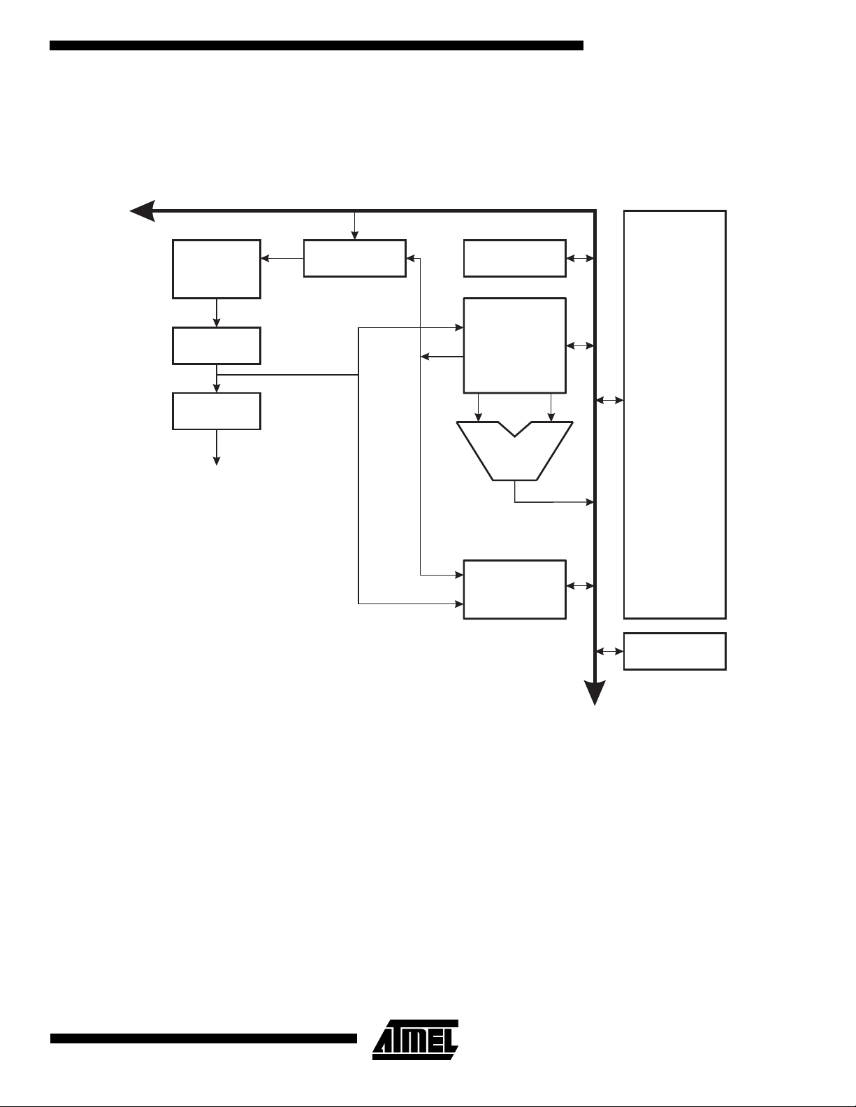
Architectural Overview
Figure 4. The ATmega603/103 AVR RISC Architecture
AVR ATmega603/103 Architecture
ATmega603/103
Data Bus 8-bit
32K/64K x 16
Program
Memory
Instruction
Register
Instruction
Decoder
Control Lines
Program
Counter
DirectAddressing
Status
and Test
32 x 8
General
Purpose
Registers
Peripherals
ALU
IndirectAddressing
4K x 8
Data
SRAM
2K/4K x 8
EEPROM
The AVR uses a Harvard architecture concept - with separate memories and buses for program and data. The program
memory is accesses with a single level pipeline. While one instruction is being executed, the next instruction is pre-fetched
from the program me mor y. This co nc ept enables instructio ns to be executed in ever y cl ock cycle. The program me mor y is
in-system programmable Flash memory. With a few exceptions, AVR instructions have a single 16-bit word format,
meaning that every program memory address contains a single 16-bit instruction.
During interrupts and subroutine c alls, the ret urn address program counter (PC) is stor ed on the st ack. The stac k is
effectively allocated in the general data SRAM, and consequently the sta ck siz e i s onl y limi ted by the total SRAM si z e an d
the usage of the SRAM. All user programs must initialize the SP in the reset routine (before subroutines or interrupts are
executed). The 16-bit stack pointer SP is read/write accessible in the I/O space.
The 4000 bytes da ta SRAM can be easily ac cessed th rough the f ive dif ferent ad dressing modes sup ported in t he AVR
architecture.
7
Page 8

A flexible interrupt module has its control registers in the I/O space with an additional global interrupt enable bit in the status
register. All the different interrupts have a separate interrupt vector in the interrupt vector table at the beginning of the
program memory. Th e diffe rent in terrupts have priority in a ccordan ce wit h thei r interr upt vect or pos ition. T he lo wer th e
interrupt vector address, the higher the priority.
The memory spaces in the AVR architecture are all linear and regular memory maps.
General Purpose Register File
Figure 5 shows the structure of the 32 general purpose working registers in the CPU.
Figure 5. AVR CPU General Purpose Working Registers
7 0 Addr.
R0 $00
R1 $01
R2 $02
. . .
R13 $0D
General R14 $0E
Purpose R15 $0F
Working R16 $10
Registers R17 $11
. . .
R26 $1A X-register low byte
R27 $1B X-register high byte
R28 $1C Y-register low byte
R29 $1D Y-register high byte
R30 $1E Z-register low byte
R31 $1F Z-register high byte
All the register opera ting instructi ons in the instructio n set have direct and single cycle access to all registe rs. The only
exception is the five consta nt arithme tic and logic in struction s SBCI, SUBI, CPI, ANDI and ORI betwe en a constan t and a
register and the LDI i nstruc tion f or load imm ediate consta nt data . Th ese ins tructi ons a pply to the s econ d hal f of t he regi sters in the register file - R16..R31. The general SBC, SUB, CP, AND and OR and all other operations between two registers
or on a single register apply to the entire register file.
As shown in Figure 5, each register is als o assigned a data memory addr ess, mapping them directly into the first 32
locations of the user Data Space. Although not being physically implemented as SRAM locations, this memory organization
provides great flexibility in access of the registers, as the X,Y and Z registers can be set to index any register in the file.
The 4K bytes of SRAM available for general data are implemented as addresses $0060 to $0FFF.
8
ATmega603/103
Page 9
ATmega603/103
X-register, Y-register and Z-register
The registers R26..R 31 ha ve some a dded funct ions to th eir general pur pose us age. These regis ters a re a ddress poi nters
for indirect addressing of the SRAM. The three indirect address registers X, Y and Z are defined as:
Figure 6. X, Y and Z Registers
15 0
X - register 7 0 7 0
R27 ($1B) R26 ($1A)
15 0
Y - register 7 0 7 0
R29 ($1D) R28 ($1C)
15 0
Z - register 7 0 7 0
R31 ($1F) R30 ($1E)
In the different addr essing modes these addres s re gisters have fu nctio ns as fixed displ acement, automat ic i ncremen t and
decrement (see the descriptions for the different instructions).
ALU - Arithmetic Logic Unit
The high-performance AVR ALU operates in direct connection with all the 32 general purpose working registers. Within a
single clock cy cl e, AL U operations between r egis ter s in the re gis te r f il e ar e exec uted . The ALU operations are div i ded in to
three main categories - arithmetic, logical and bit-functions.
ISP Flash Program Memory
The ATmega603/103 contains 64K/128K bytes on-chip In-system Programmable Flash memory for program storage.
Since all instructio ns are single or dou ble 16-bit word s, the Flash is orga nized as 64K x 16. The Flash memory has an
endurance of at least 1000 write/erase cycles.
Constant tables can be allocated in the entire program memory space (see the LPM - Load Program Memory and ELPM
Extended Load Program Memory instruction descriptions).
SRAM Data Memory
The ATmega603/103 supports two different configurations for the SRAM data memory as listed in the following table:
Table 2. Memory Configurations
Configuration Internal SRAM Data Memory External SRAM Data Memory
A 4000 None
B 4000 up to 64K
Note: When using 64K of External SRAM, 60K will be available.
9
Page 10
Figure 7. Memory Configurations
Memory Configuration A
Program Flash
(32K/64K x 16)
$0000
Data MemoryProgram Memory
32 Registers
64 I/O Registers
Internal SRAM
(4000 x 8)
$0000 - $001F
$0020 - $005F
$0060
$0FFF
Memory Configuration B
Program Memory
Program Flash
(32K/64K x 16)
$7FFF/$FFFF
$0000
Data Memory
32 Registers
64 I/O Registers
Internal SRAM
(4000 x 8)
External SRAM
(0 - 64K x 8)
$0000 - $001F
$0020 - $005F
$0060
$0FFF
$1000
10
ATmega603/103
$7FFF/
$FFFF
$FFFF
Page 11
ATmega603/103
The 4096 first Data Memory locations address both the Register file, the I/O Memory and the internal data SRAM. The first
96 locations address the register file and I/O memory, and the next 4000 locations address the internal data SRAM.
An optional external data SRAM can be used with the ATmega603/103. This SRAM will occupy an area in the remaining
address locations in the 64K ad dr ess s pa ce . Thi s a rea s tarts at t he a ddr es s fol lowing the internal SRAM. If a 64K ex terna l
SRAM is used, 4K of the external memory is lost as the addresses are occupied by internal memory.
When the addresses accessing the SRAM memory space exceeds the internal data memory locations, the external data
SRAM is accesse d using t he sam e ins tructio ns as for the inter nal da ta memo ry acces s. W hen the internal data m emor ies
are accessed, the read and write strobe pins (RD
operation is enabled by setting the SRE bit in the MCUCR register.
Accessing external SRAM takes one additional clock cycle per byte compared to access of the internal SRAM. This means
that the commands LD, ST, LDS, STS, PUSH and POP take one additional clock cycle. If the stack is placed in external
SRAM, interrupts, subroutine call s and returns take two clock cycles extra because the two- byte program counter is
pushed and popped. When external SRAM interface is used with wait state, two additional clock cycles is used per byte.
This has the following e ffec t: Da ta tran sfer instructions take two extr a cl oc k cy c les, wh er eas in terr upt, su br outine c al ls an d
returns will need four clock cycles more than specified in the instruction set manual.
The five different addressing modes for the data memory cover: Direct, Indirect with Displacement, Indirect, Indirect with
Pre-Decrement and Indirect with Post-Increment. In the register file, registers R26 to R31 feature the indirect addressing
pointer registers.
The Indirect with Displacement mode features a 63 address locations reach from the base address given by the Y or
Z-register.
When using register indirect addressing modes with automatic pre-decrement and post-increment, the address registers X,
Y and Z are decremented and incremented.
The entire data addres s sp ac e in cl ud ing the 32 gene ra l p ur pose wor ki ng regis te rs an d th e 64 I/O r egi s ters ar e al l ac cess ible through all these addressing modes. See the next section for a detailed description of the different addressing modes.
and WR) are inactive during the whole acce ss cycle. Ex ternal SRA M
Program and Data Addressing Modes
The ATmega603/103 AV R RISC microco ntroller supports po werful and effi cient addressing modes for acc ess to the
program memory (Flash) and data memory ( SRAM, Register File and I/O M emory). This se ction descr ibes the different
addressing modes suppor ted by the AVR a rchitectur e. In the f igures, OP means the o peration code par t of th e ins tructio n
word. To simplify, not all figures show the exact location of the addressing bits.
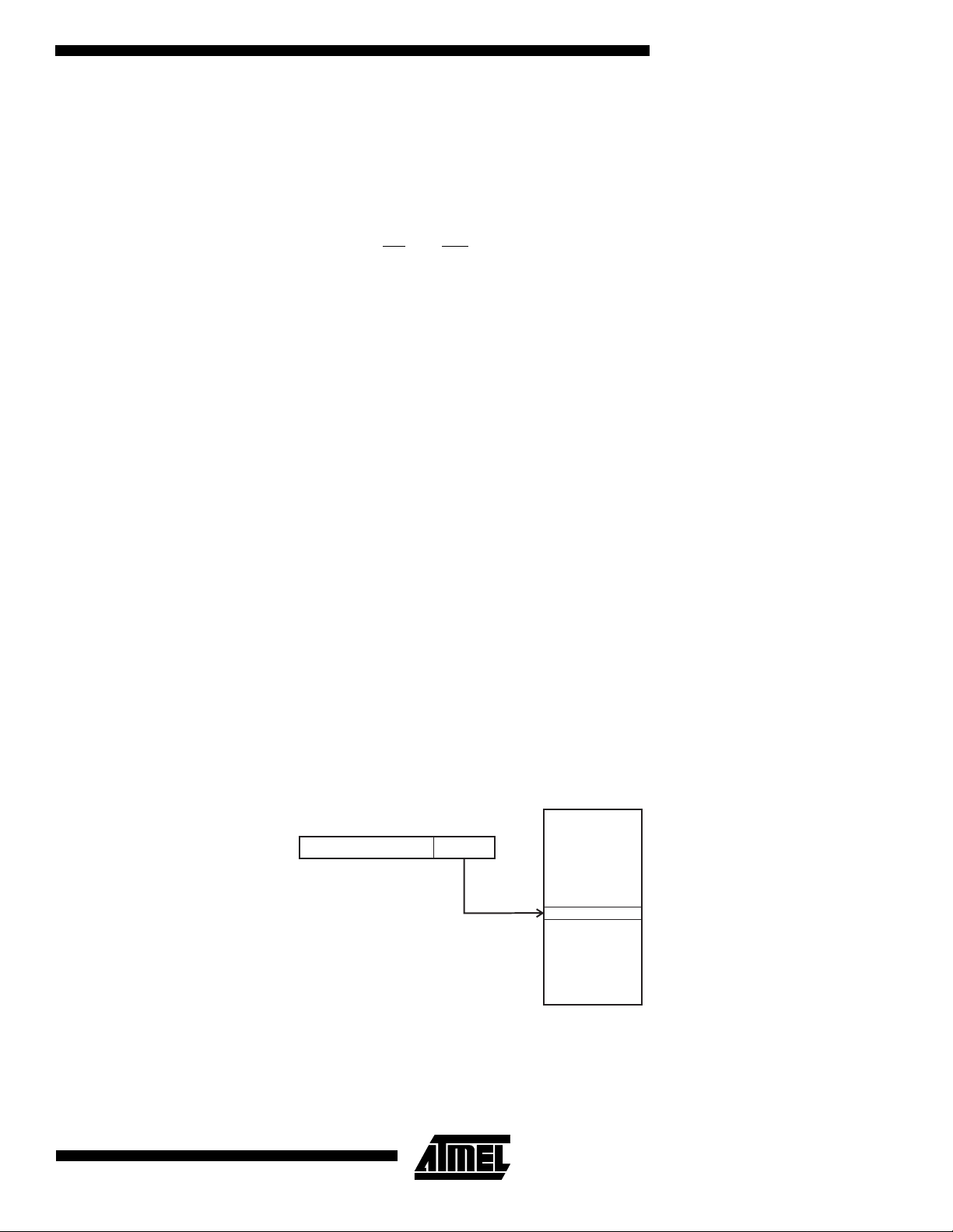
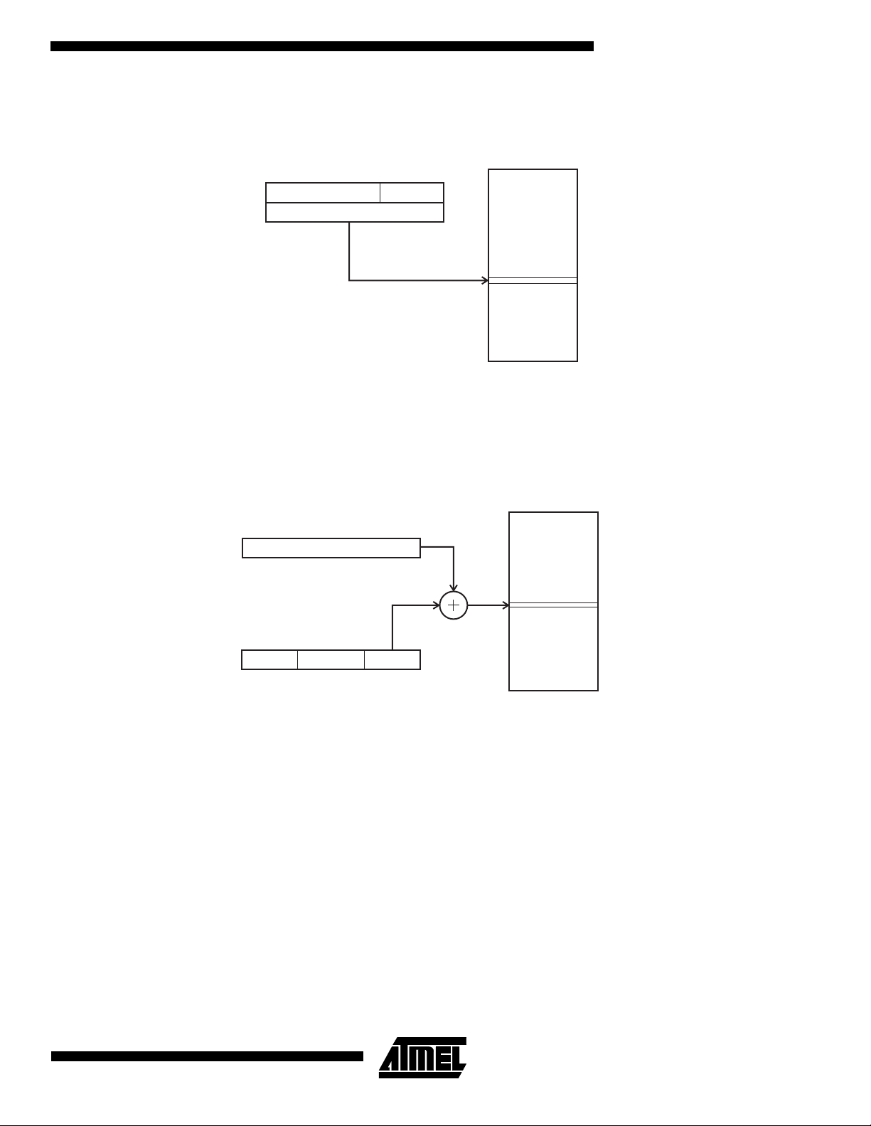
Register Direct, Single Register Rd
Figure 8. Direct Single Register Addressing
15
The operand is contained in register d (Rd).
REGISTER FILE
04
OP d
0
d
31
11
Page 12
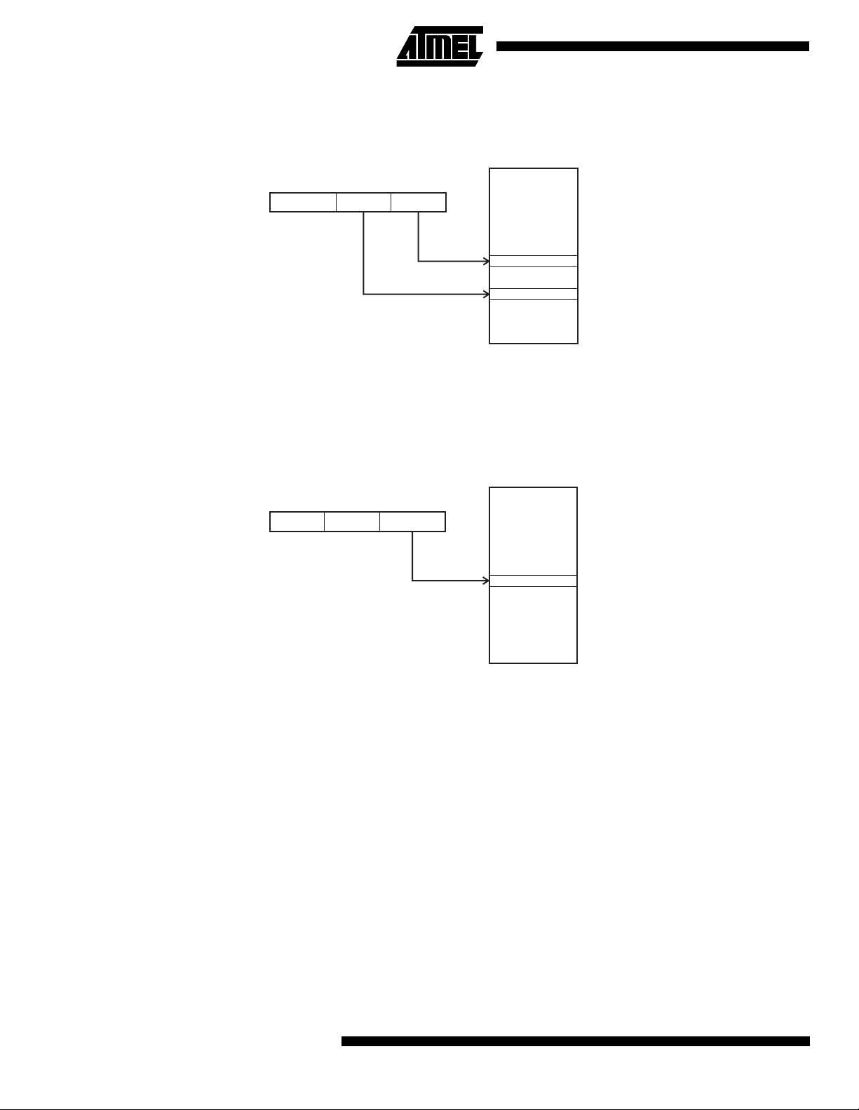
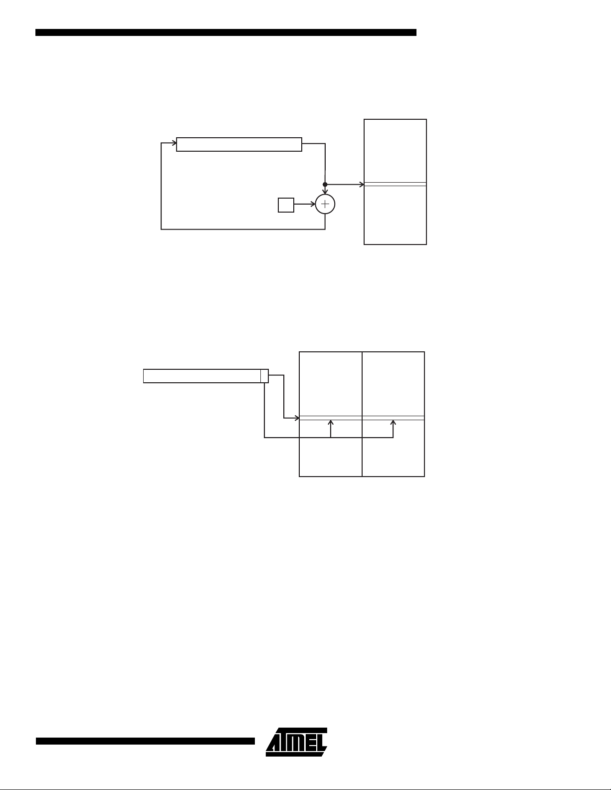
Register Direct, Two Registers Rd and Rr
Figure 9. Direct Register Addressing, Two Registers
15
REGISTER FILE
0459
OP dr
0
d
r
31
Operands are contained in register r (Rr) and d (Rd). The result is stored in register d (Rd).
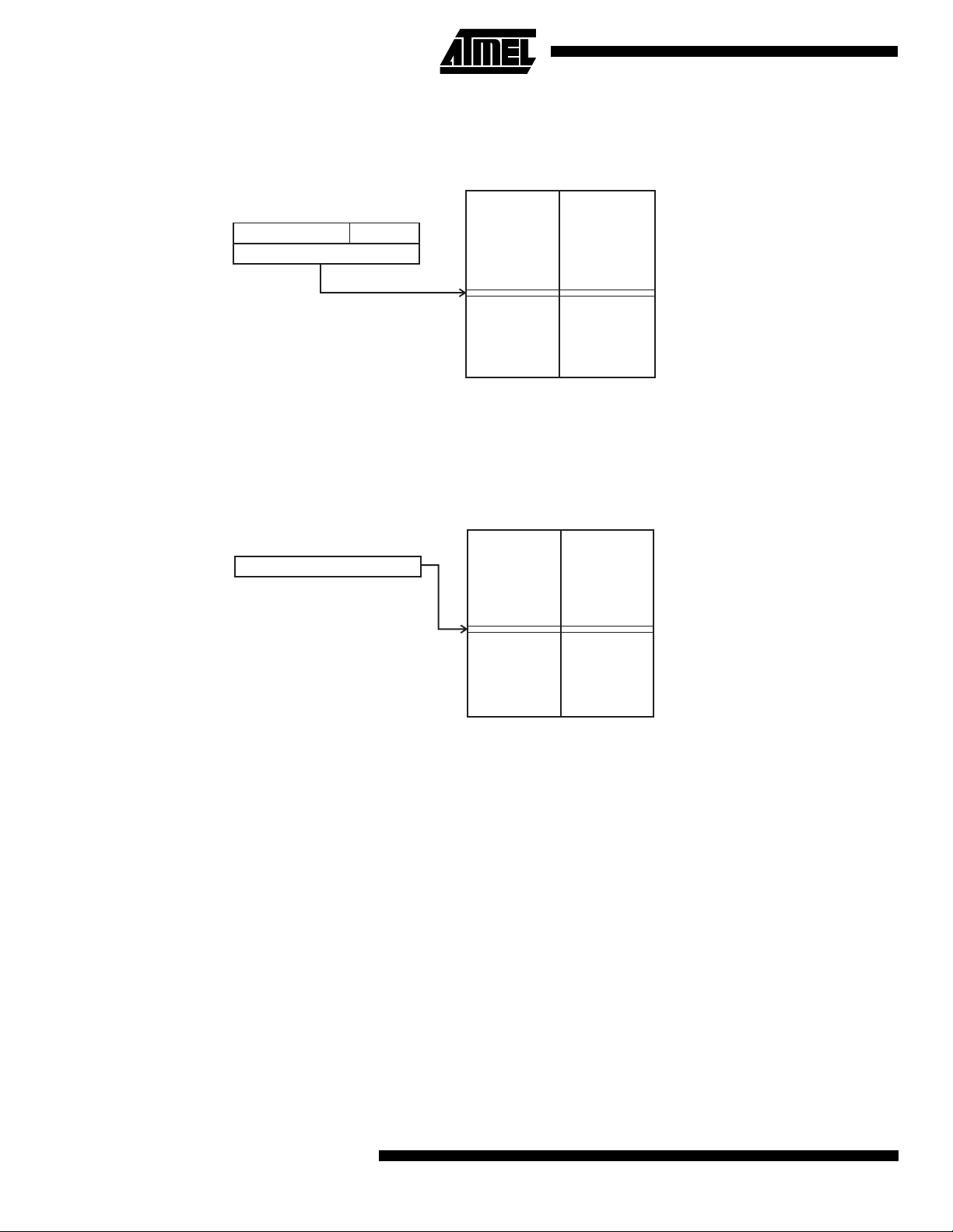
I/O Direct
Figure 10. I/O Direct Addressing
15
OP P
n
I/O MEMORY
05
0
63
Operand address is contained in 6 bits of the instruction word. n is the destination or source register address.
12
ATmega603/103
Page 13
ATmega603/103
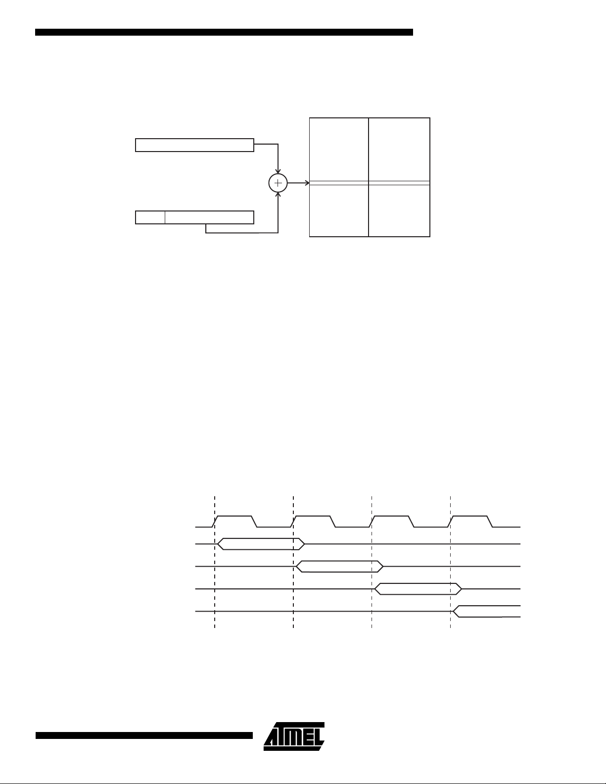
Data Direct
Figure 11. Direct Data Addressing
31
OP Rr/Rd
15 0
20 19
16 LSBs
16
Data Space
A 16-bit Data Address is contained in the 1 6 LSBs of a two-word instruction. Rd/Rr s pecify the destination or source
register.
Data Indirect with Displacement
$0000
$FFFF
Figure 12. Data Indirect with Displacement
15
Y OR Z - REGISTER
15
OP an
Data Space
0
05610
$0000
$FFFF
Operand address is the re sult of the Y or Z-register contents added to the address contained in 6 bits of the in struction
word.
13
Page 14

Data Indirect
Figure 13. Data Indirect Addressing
015
X, Y OR Z - REGISTER
Operand address is the contents of the X, Y or the Z-register.
Data Indirect With Pre-Decrement
Figure 14. Data Indirect Addressing with Pre-Decrement
015
X, Y OR Z - REGISTER
Data Space
Data Space
$0000
$FFFF
$0000
-1
$FFFF
The X, Y or the Z- regi ste r i s dec r eme nte d b efor e th e o peration. Operand addr es s is the decremented con tent s of the X, Y
or the Z-register.
14
ATmega603/103
Page 15
ATmega603/103
Data Indirect With Post-Increment
Figure 15. Data Indirect Addressing with Post-Increment
Data Space
015
X, Y OR Z - REGISTER
1
The X, Y or the Z-r egister is incr emen ted a fter the ope rati on. O perand addr ess is t he c onten t of the X , Y or t he Z-r egister
prior to incrementing.
Constant Addressing Using the LPM and ELPM Instructions
$0000
$FFFF
Figure 16. Code Memory Constant Addressing
PROGRAM MEMORY
0115
Z - REGISTER
$0000
$7FFF/$FFFF
Constant byte address is specified by the Z-register contents. The 15 MSBs select word address (0 - 32K), LSB selects low
byte if cleared (LSB = 0) or high byte if set (LSB = 1). If ELPM is used, LSB of the RAM Page Z register - RAMPZ is used to
select low or high memory page (RAMPZ0 = 0: Low Page, RAMPZ0 = 1: High Page). ELPM does not apply to the
ATmega603.
15
Page 16
Direct Program Address, JMP and CALL
Figure 17. Direct Program Memory Addressing
PROGRAM MEMORY
31
OP
15 0
21 20
16 LSBs
16
Program execution continues at the address immediate in the instruction words.
Indirect Program Addressing, IJMP and ICALL
Figure 18. Indirect Program Memory Addressing
PROGRAM MEMORY
015
Z - REGISTER
$0000
$7FFF/$FFFF
$0000
$7FFF/$FFFF
Program execution continues at address contained by the Z-register (i.e. the PC is loaded with the contents of the
Z-register).
16
ATmega603/103
Page 17
Relative Program Addressing, RJMP and RCALL
Figure 19. Relative Program Memory Addressing
15
PC
0
PROGRAM MEMORY
ATmega603/103
$0000
15
1112
OP k
Program execution continues at address PC + k + 1. The relative address k is -2048 to 2047.
0
$7FFF/$FFFF
EEPROM Data Memory
The EEPROM memory is organized as a separate data space, in which single bytes can be read and written. The
EEPROM has an endura nce of at leas t 100,000 wr ite/erase cy cles. The access betwe en the EEPROM and the CPU is
described on pa ge 52 specif ying th e EEPR OM a ddress r egiste r, the EEPROM data r egister , and t he EEP ROM co ntrol
register.
Memory Access Times and Instruction Execution Timing
This section describes the general access timing concepts for instruction execution and internal memory access.
The AVR CPU is driven b y the S yste m Clock Ø, di rectly gener ated from the ex ternal c lock c rystal for the c hip. No interna l
clock division is used.
Figure 20 shows the parallel instructio n fetches and instructio n executions enabl ed by the Harvard architec ture and the
fast-access register file concept. This is the basic pipelining concept to obtain up to 1 MIPS per MHz with the corresponding
unique results for functions per cost, functions per clocks, and functions per power-unit.
Figure 20. The Parallel Instruction Fetches and Instruction Executions
T1 T2 T3 T4
System Clock Ø
1st Instruction Fetch
1st Instruction Execute
2nd Instruction Fetch
2nd Instruction Execute
3rd Instruction Fetch
3rd Instruction Execute
4th Instruction Fetch
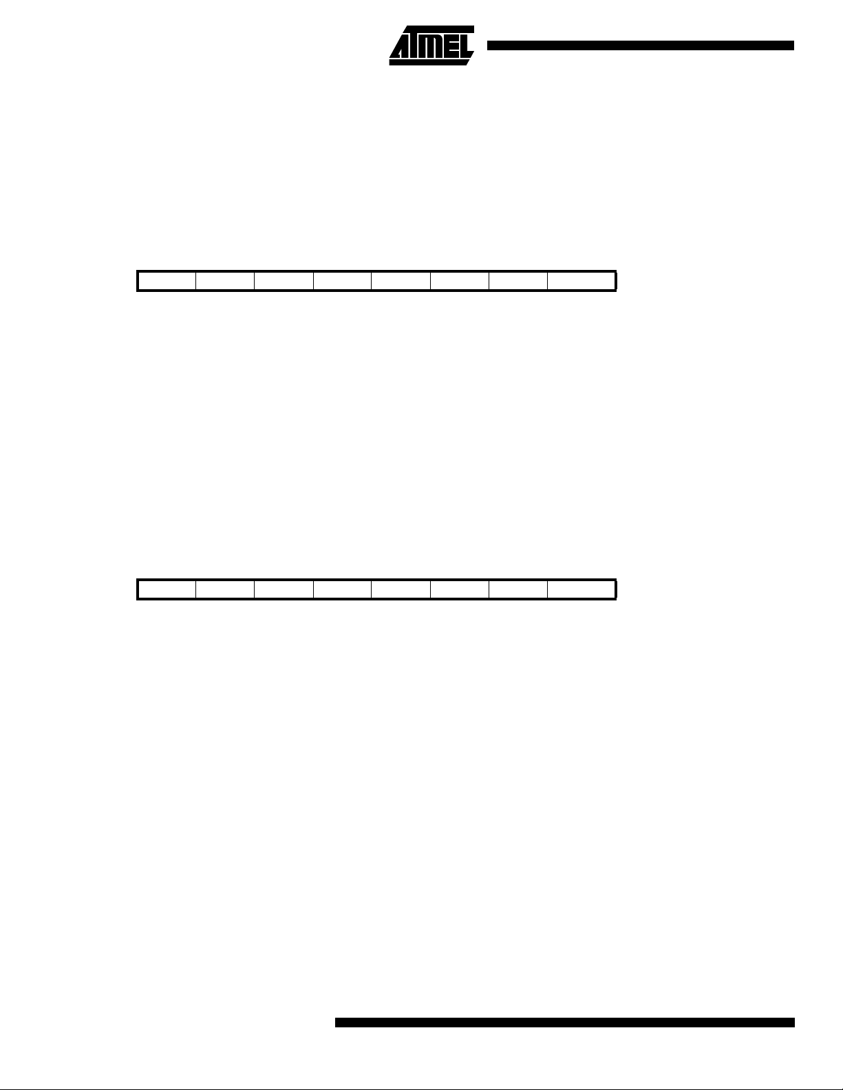
Figure 21 shows the internal timing concept for the register file. In a single clock cycle an ALU operation using two register
operands is executed, and the result is stored back to the destination register.
17
Page 18
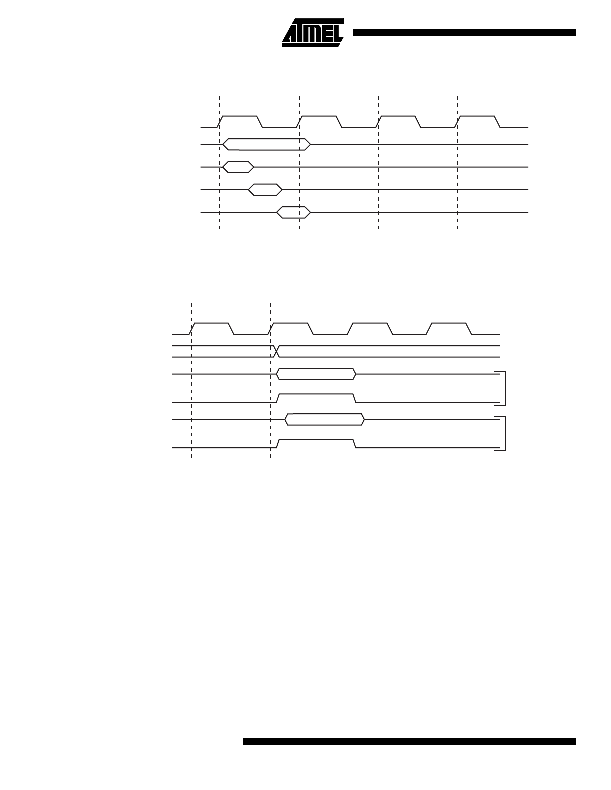
Figure 21. Single Cycle ALU Operation
T1 T2 T3 T4
System Clock Ø
Total Execution Time
Register Operands Fetch
ALU Operation Execute
Result Write Back
The internal data SRAM access is performed in two System Clock cycles as described in Figure 22.
Figure 22. On-Chip Data SRAM Access Cycles
T1 T2 T3 T4
System Clock Ø
Address
Prev. Address
Address
Data
WR
Data
RD
See “Interface to external SRAM” on page 72 for a description of the access to the external SRAM.
Read Write
18
ATmega603/103
Page 19

I/O Memory
The I/O space definition of the ATmega603/103 is shown in the following table:
Table 3. ATmega603/103 I/O Space
I/O Address (SRAM Address) Name Function
$3F ($5F) SREG Status REGister
$3E ($5E) SPH Stack Pointer High
$3D ($5D) SPL Stack Pointer Low
$3C ($5C) XDIV XT AL Divi de Control Regi ster
$3B ($5B) RAMPZ RAM Page Z Select Register
$3A ($5A) EICR External Interrupt Control Register
$39 ($59) EIMSK External Interrupt MaSK register
$38 ($58) EIFR External Interrupt Flag Register
$37 ($57) TIMSK Timer/Counter Interrupt MaSK register
$36 ($56) TIFR Timer/Counter Interrupt Flag register
$35 ($55) MCUCR MCU General Control Register
ATmega603/103
$34 ($54) MCUSR MCU Status Register
$33 ($53) TCCR0 Timer/Counter0 Control Register
$32 ($52) TCNT0 Timer/Counter0 (8-bit)
$31 ($51) OCR0 Timer/Counter0 Output Compare Register
$30 ($50) ASSR Asynchronous Mode Status Register
$2F ($4F) TCCR1A Timer/Counter1 Control Register A
$2E ($4E) TCCR1B Timer/Counter1 Control Register B
$2D ($4D) TCNT1H Timer/Counter1 High Byte
$2C ($4C) TCNT1L Timer/Counter1 Low Byte
$2B ($4B) OCR1AH Timer/Counter1 Output Compare Register A High Byte
$2A ($4A) OCR1AL Timer/Counter1 Output Compare Register A Low Byte
$29 ($49) OCR1BH Timer/Counter1 Output Compare Register B High Byte
$28 ($48) OCR1BL Timer/Counter1 Output Compare Register B Low Byte
$27 ($47) ICR1H Timer/Counter1 Input Capture Register High Byte
$26 ($46) ICR1L Timer/Counter1 Input Capture Register Low Byte
$25 ($45) TCCR2 Timer/Counter2 Control Register
$24 ($44) TCNT2 Timer/Counter2 (8-bit)
$23 ($43) OCR2 Timer/Counter2 Output Compare Register
$21 ($41) WDTCR Watchdog Timer Control Register
$1F ($3F) EEARH EEPROM Address Register High
$1E ($3E) EEARL EERPOM Address Register Low
$1D ($3D) EEDR EEPROM Data Register
$1C ($3C) EECR EEPROM Control Register
19
Page 20

Table 3. ATmega603/103 I/O Space (Continued)
I/O Address (SRAM Address) Name Function
$1B ($3B) PORTA Data Register, Port A
$1A ($3A) DDRA Data Direction Register, Port A
$19 ($39) PINA Input Pins, Port A
$18 ($38) PORTB Data Register, Port B
$17 ($37) DDRB Data Direction Register, Port B
$16 ($36) PINB Input Pins, Port B
$15 ($35) PORTC Data Register, Port C
$12 ($32) PORTD Data Register, Port D
$11 ($31) DDRD Data Direction Register, Port D
$10 ($30) PIND Input Pins, Port D
$0F ($2F) SPDR SPI I/O Data Register
$0E ($2E) SPSR SPI Status Register
$0D ($2D) SPCR SPI Control Register
$0C ($2C) UDR UART I/O Data Register
$0B ($2B) USR UART Status Register
$0A ($2A) UCR UART Control Register
$09 ($29) UBRR UART Baud Rate Register
$08 ($28) ACSR Analog Comparator Control and Status Register
$07 ($27) ADMUX ADC Multiplexer Select Register
$06 ($26) ADCSR ADC Control and Status Register
$05 ($25) ADCH ADC Data Register High
$04 ($24) ADCL ADC Data Register Low
$03 ($23) PORTE Data Register, Port E
$02 ($22) DDRE Data Direction Register, Port E
$01 ($21) PINE Input Pins, Port E
$00 ($20) PINF Input Pins, Port F
Note: Reserved and unused locations are not shown in the table
All the different ATmega603/103 I/Os and peripherals are placed in the I/O space. The different I/O locations are directly
accessed by the IN and OUT ins truct ions transf erring data be tween the 32 ge neral purp ose workin g register s and the I/O
space. I/O registers within the address range $00 - $1F are directly bit-accessible using the SBI and CBI instructions. In
these registers, the value of single bits can be checked by using the SBIS and SBIC instructions. Refer to the instruction
set chapter for more details. When using the I/O specific instructions IN, OUT, the I/O register address $00 - $3F are used.
When addressing I/O registers as SRAM, $20 must be added to this address. All I/O r egister addresses throughout this
document are shown with the SRAM address in parentheses.
For compatibility with future devices, res er ve d b its s hou ld be wr itte n t o z er o i f a cces s ed. Res erve d I/ O mem or y add re ss es
should never be written.
Some of the status flags are cleared by writing a logical one to them. Note that the CBI and SBI instructions will operate on
all bits in the I/O regi ster , writing a one ba ck in to any flag read as s et, thus cl earing t he f lag. The C BI and SB I instr ucti ons
work with registers $00 to $1F only.
20
ATmega603/103
Page 21

ATmega603/103
The different I/O and peripherals control registers are explained in the following sections.
Status Register - SREG
The AVR status register - SREG - at I/O space location $3F ($5F) is defined as:
Bit 76543210
$3F ($5F) I T H S V N Z C SREG
Read/Write R/W R/W R/W R/W R/W R/W R/W R/W
Initial value00000000
•
Bit 7 - I: Global Interrupt Enable
The global interr upt e nable bit must be set (one ) for the i nterrup ts to be e nable d. The indi vidu al in terrup t enab le c ontrol is
then performed in s eparate con trol regi sters. If the globa l inte rru pt ena ble r egist er is clear ed (zero ), non e of the i nter rupts
are enabled independent of the individual interrupt enable settings. The I-bit is cleared by hardware after an interrupt has
occurred, and is set by the RETI instruction to enable subsequent interrupts.
Bit 6 - T: Bit Copy Storage
•
The bit copy instructions BLD (Bit LoaD) and BST (Bit STore) use the T bit as source and destination for the operated bit. A
bit from a register in the regi ste r file can be copied into T by the BST instru ct ion , and a bit i n T can be c opi ed i nto a bit in a
register in the register file by the BLD instruction.
Bit 5 - H: Half Carry Flag
•
The half carry flag H indicates a half carry in some arithmetic operations. See the Instruction Set Description for detailed
information.
Bit 4 - S: Sign Bit, S = N ⊕ V
•
The S-bit is always an exclusive or between the negative flag N and the two’s complement overflow flag V. See the Instruc-
tion Set Description for detailed information.
Bit 3 - V: Two’s Complement Overflow Flag
•
The two’s complement overflow flag V supports two’s complement arithmetics. See the Instruction Set Description for
detailed information.
Bit 2 - N: Negative Flag
•
The negative flag N indicates a negative result from an arithmetical or logical operation. See the Instruction Set Description
for detailed information.
Bit 1 - Z: Zero Flag
•
The zero flag Z indi cates a zero r esult from an arithmetic al or logical operation. See the Instru ction Se t Descriptio n for
detailed information.
Bit 0 - C: Carry Flag
•
The carry flag C indicates a carry in an ari thmetical or logical opera tion. See the Instruction Se t Description for detailed
information.
Note that the status register is not automatically stored when entering an interrupt routine and restored when returning from
an interrupt routine. This must be handled by software.
Stack Pointer - SP
The general AVR 16-bit Stack Poin ter is effecti vely built up of two 8- bit registe rs in the I/O s pace loca tions $3E ($5E ) and
$3D ($5D). As the ATmega603/103 supports up to 64 kB memory, all 16-bits are used.
Bit 151413121110 9 8
$3E ($5E) SP15 SP14 SP13 SP12 SP11 SP10 SP9 SP8 SPH
$3D ($5D) SP7 SP6 SP5 SP4 SP3 SP2 SP1 SP0 SPL
76543210
Read/Write R/W R/W R/W R/W R/W R/W R/W R/W
R/W R/W R/W R/W R/W R/W R/W R/W
Initial value00000000
00000000
21
Page 22
The Stack Pointe r poin ts to the da ta SRA M st ack a rea where t he Subrou tine and I nte rrupt Stac ks are lo cated . Th is Sta ck
space in the d ata SRAM m ust be defi ned by the p rogram befor e any su broutine cal ls are execu ted or in terrupts are
enabled. The stack pointer must be set to point above $60. The Stack Pointer is decremented by one when data is pushed
onto the Stack with the PUSH instruction, and it is decremented by two when an address is pushed onto the Stack with
subroutine calls and interrupts. The Stack Pointer is incremented by one when data is popped from the Stack with the POP
instruction, and it is incremente d by two when an address i s popped from the Stac k with return from subr outine RET or
return from interrupt RETI.
RAM Page Z Select Register - RAMPZ
Bit 7654321 0
$3B ($5B) - - - - - - - RAMPZ0 RAMPZ
Read/WriteRRRRRRRR/W
Initial value0000000 0
The RAMPZ register is normally used to select which 64K RAM Page is accessed by the Z pointer. As the ATmega603/103
does not support more than 64K of SRAM memory , this regi ster is use d only to se lect whi ch page in the program memo ry
is accessed when the ELPM instruction is used. The different settings of the RAMPZ0 bit have the following effects:
RAMPZ0 = 0: Program memory address $0000- $7FFF (lower 64K bytes) is accessed by ELPM
RAMPZ0 = 1: Program memory address $8000- $FFFF (higher 64K bytes) is accessed by ELPM
Note that LPM is not affected by the RAMPZ setting.
The ATmega603 does not contain the RAMPZ register, and it does not have the ELPM instruction. The ordinary LPM
instruction can reach the entire program memory in the ATmega603.
MCU Control Register - MCUCR
The MCU Control Register contains control bits for general MCU functions.
Bit 7654321 0
$35 ($55) SRE SRW SE SM1 SM0 - - - MCUCR
Read/Write R/W R/W R/W R/W R/W R R R
Initial value0000000 0
•
Bit 7 - SRE: External SRAM Enable
When the SRE bit is set (one), the externa l data SRAM is enabl ed, and the pin func tions AD0- 7 (Port A), and A8-15 (P ort
C) are activated as the al ternate pin functions. Then the SRE b it ove r rides a ny pi n d ir ecti on s et tin gs in the respective da ta
direction registers. When the SRE bit is cleared (zero), the external data SRAM is disabled, and the normal pin and data
direction settings are used.
Bit 6 - SRW: External SRAM Wait State
•
When the SRW bit is set ( one ), a one cycle wait state is ins ert ed in the ex terna l d ata SRA M a cces s c ycle . W hen the SRW
bit is cleared (zero), the external data SRAM access is executed with a three-cycle scheme. See Figure 51.External
SRAM Access Cycle without wait states73 and Figure 52.External SRAM Access Cycle with wait state74.
Bit 5 - SE: Sleep Enable
•
The SE bit must be set (one) to make the MCU enter the sleep mode when the SLEEP instruction is executed. To avoid the
MCU entering the sleep mode unless it is the programmers purpose, it is recommended to set the Sleep Enable SE bit just
before the execution of the SLEEP instruction.
22
ATmega603/103
Page 23

ATmega603/103
•
Bits 4,3 - SM1/SM0: Sleep Mode Select bits 1 and 0
This bit selects between the three available sleep modes as shown in the following table:
Table 4. Sleep Mode Select
SM1 SM0 Sleep Mode
0 0 Idle Mode
01Reserved
1 0 Power Down
1 1 Power Save
Bits 2..0 - Res: Reserved bits
•
These bits are reserved bits in the ATmega603/103 and always read zero.
XTAL Divide Control Register - XDIV
The XTAL Divide Contr ol Reg ister is used to di vide the X TAL cl ock fr equenc y by a numbe r in the rang e 1 - 129. This f eature can be used to decrease power consumption when the requirement for processing power is low.
Bit 7 654321 0
$3C ($5C) XDIVEN XDIV6 XDIV5 XDIV4 XDIV3 XDIV2 XDIV1 XDIV0 XDIV
Read/Write R/W R/W R/W R/W R/W R/W R/W R/W
Initial value0 000000 0
Bit 7 - XDIVEN: XTAL Divide Enable
•
When the XDIVEN bit is set (one), the clock frequency of the CPU and all peripherals is divided by the factor defined by the
setting of XDIV6 - XDIV0. This bit can be set and cleared run-time to vary the clock frequency as suitable to the application.
Bits 6..0 - XDIV6..XDIV0: XTAL Divide Select Bits 6 - 0
•
These bits define the division factor that applies when the XDIVEN bit is set (one). If the value of these bits is denoted d,
f
the following formula defines the resulting CPU clock frequency
f
CLK
clk
XTAL
------------------ -=
129 d–
:
The value of these bits can only be ch ange d when XDIV EN i s ze ro. Whe n XDIVEN is set to one, the value written si multaneously into XDIV6..XDIV0 is taken as the division factor. When XDIVEN is cleared to zero, the value written
simultaneously into XDIV6..XDIV0 is rejected. As the divider divides the master clock input to the MCU, the speed of all
peripherals is reduced when a division factor is used.
23
Page 24

Reset and Interrupt Handling
The ATmega603/103 provides 23 different interrupt sources. These interrupts and the separate reset vector each have a
separate program vector in the program memory space. All interrupts are assigned individual enable bits which must be set
(one) together with the I-bit in the status register in order to enable the interrupt.
The lowest addresses i n the pro gram memory s pace are aut omatically defined a s the Reset an d Interru pt vectors. The
complete list of vectors is shown in Table 5. The list also determines the priority levels of the different interrupts. The lower
the address the higher is the priority level. RESET has the highest priority, and next is INT0 - the External Interrupt Request
0 etc.
Table 5. Reset and Interrupt Vectors
Vector No. Program Address Source Interrupt Definition
1 $0000 RESET Hardware Pin, Power-on Reset and Watchdog Reset
2 $0002 INT0 External Interrupt Request 0
3 $0004 INT1 External Interrupt Request 1
4 $0006 INT2 External Interrupt Request 2
5 $0008 INT3 External Interrupt Request 3
6 $000A INT4 External Interrupt Request 4
7 $000C INT5 External Interrupt Request 5
8 $000E INT6 External Interrupt Request 6
9 $0010 INT7 External Interrupt Request 7
10 $0012 TIMER2 COMP Timer/Counter2 Compare Match
11 $0014 TIMER2 OVF Timer/Counter2 Overflow
12 $0016 TIMER1 CAPT Timer/Counter1 Capture Event
13 $0018 TIMER1 COMPA Timer/Counter1 Compare Match A
14 $001A TIMER1 COMPB Timer/Counter1 Compare Match B
15 $001C TIMER1 OVF Timer/Counter1 Overflow
16 $001E TIMER0 COMP Timer/Counter0 Compare Match
17 $0020 TIMER0 OVF Timer/Counter0 Overflow
18 $0022 SPI, STC SPI Serial Transfer Complete
19 $0024 UART, RX UART, Rx Complete
20 $0026 UART, UDRE UART Data Register Empty
21 $0028 UART, TX UART, Tx Complete
22 $002A ADC ADC Conversion Complete
23 $002C EE READY EEPROM Ready
24 $002E ANALOG COMP Analog Comparator
24
ATmega603/103
Page 25

The most typical program setup for the Reset and Interrupt Vector Addresses are:
Address Labels Code Comments
$0000 jmp RESET ; Reset Handler
$0002 jmp EXT_INT0 ; IRQ0 Handler
$0004 jmp EXT_INT1 ; IRQ1 Handler
$0006 jmp EXT_INT2 ; IRQ2 Handler
$0008 jmp EXT_INT3 ; IRQ3 Handler
$000A jmp EXT_INT4 ; IRQ4 Handler
$000C jmp EXT_INT5 ; IRQ5 Handler
$000E jmp EXT_INT6 ; IRQ6 Handler
$0010 jmp EXT_INT7 ; IRQ7 Handler
$0012 jmp TIM2_COMP ; Timer2 Compare Handler
$0014 jmp TIM2_OVF ; Timer2 Overflow Handler
$0016 jmp TIM1_CAPT ; Timer1 Capture Handler
$0018 jmp TIM1_COMPA ; Timer1 CompareA Handler
$001A jmp TIM1_COMPB ; Timer1 CompareB Handler
$001C jmp TIM1_OVF ; Timer1 Overflow Handler
$001E jmp TIM0_COMP ; Timer0 Compare Handler
$0020 jmp TIM0_OVF ; Timer0 Overflow Handler
$0022 jmp SPI_STC ; SPI Transfer Complete Handler
$0024 jmp UART_RXC ; UART RX Complete Handler
$0026 jmp UART_DRE ; UDR Empty Handler
$0028 jmp UART_TXC ; UART TX Complete Handler
$002A jmp ADC ; ADC Conversion Complete Handler
$002C jmp EE_RDY ; EEPROM Ready Handler
$002E jmp ANA_COMP ; Analog Comparator Handler
;
$0030 MAIN: ldi r16, high(RAMEND); Main program start
$0031 out SPH,r16
$0032 ldi r16, low(RAMEND)
$0033 out SPL,r16
$0034 <instr> xxx
... ... ... ...
ATmega603/103
Reset Sources
The ATmega603/103 has three sources of reset:
• Power-On Reset. The MCU is reset when the supply voltage is below the power-on reset threshold (V
• External Reset. The MCU is reset when a low level is present on the RESET
pin for more than 50 ns.
POT
).
• Watchdog Reset. The MCU is reset when the Watchdog timer period expires and the Watchdog is enabled.
During reset, all I/O registers except the MCU Status register are then set to their initial values, and the program starts exe-
cution from address $0000. The instruction placed in address $0000 must be a JMP - absolute jump instruction to the reset
handling routine. If the program never enables an interrupt source, the interrupt vectors are not used, and regular program
code can be placed at these locations. The circuit diagram in Figure 23 shows the reset logic. Table 6 defines the timing
and electrical parameters of the reset circuitry.
25
Page 26
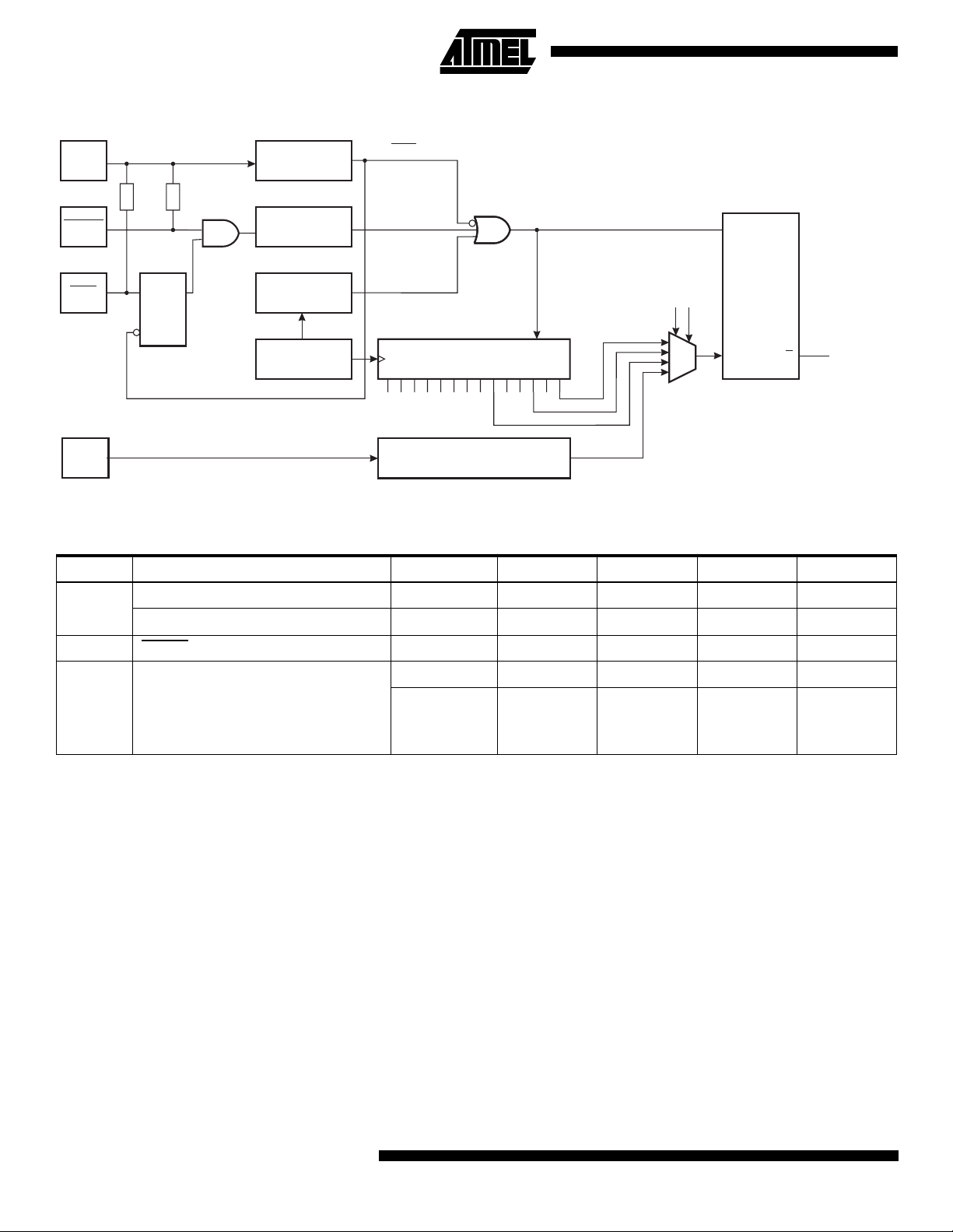
Figure 23. Reset Logic
VCC
RESET
PEN D Q
XTAL1
10-50K
E
100-500K
Power-On Reset
Circuit
Reset Circuit
Watchdog
Timer
On-Chip
RC-Oscillator
POR
14-Stage Ripple Counter
Q8 Q11 Q13
Delay Unit
COUNTER RESET
SUT0
SUT1
QS
R
Q
Table 6. Reset Characteristics (VCC = 5V)
Symbol Parameter Condition Min Typ Max Units
Power-On Reset Threshold (rising) 1.0 1.4 1.8 V
(1)
V
POT
Power-On Reset Threshold (falling) 0.4 0.6 0.8 V
INTERNAL
RESET
V
RST
RESET Pin Threshold Voltage VCC/2 V
SUT = 00 5 CPU cycles
T
TOUT
Reset Delay Time-Out Period
SUT = 01
SUT = 10
SUT = 11
0.4
3.2
12.8
Note: 1. The Power-On Reset will not work unless the supply voltage has been below V
0.5
4.0
16.0
POT
(falling)
0.6
4.8
19.2
ms
26
ATmega603/103
Page 27
ATmega603/103
Power-On Reset
A Power-On Reset (POR ) circuit ensures tha t the device is reset from power-on. As s hown in Figure 23, an inter nal timer
clocked from the Watchd og timer oscillator prevents the MCU from st arting until after a cer tain period after V
reached the Power-O n Th resh old v ol tage - V
, regardless of the VCC rise time (see Fi gure 24) . The Fu se bits SUT1 and
POT
SUT0 is used to select start-up time as indicated in Table 6. A “0” in the table indicates that the fuse is programmed.
The user can select the start-up time according to typical oscillator start-up time. The number of WDT oscillator cycles used
for each time-out ex cept for S UT = 00 is sho wn in Tabl e 7. The f requency of the w atchdo g osc illator is volta ge depe ndent
as shown in “Typical characteristics” on page 110.
Table 7. Number of watchdog oscillator cycles
SUT 1/0 Time-out at VCC = 5V Number of WDT cycles
01 0.5 ms 512
10 4.0 ms 4K
11 16.0 ms 16K
The setting SUT 1/0 = 00 starts the MCU after 5 CPU clock cycles, and can be used when an external clock signal is
applied to the XTAL1 pin. This setting does not use the WDT oscillator, and enables very fast start-up from the sleep
modes power down or power save if the clock si gnal is pr esent du ring sleep. For details, r efer to the prog ramming speci fication starting on page 92.
If the built-in start-up delay is sufficient, RESET
ing the pin low for a period after V
has been applied, the Power-On Reset period can be extended. Refer to Figure 25 for
CC
can be connected to VCC directly or via an external pull-up resistor. By hold-
a timing example on this.
CC
has
Figure 24. MCU Start-Up, RESET
VCC
RESET
TIME-OUT
INTERNAL
RESET
Tied to VCC.
V
POT
V
RST
t
TOUT
27
Page 28
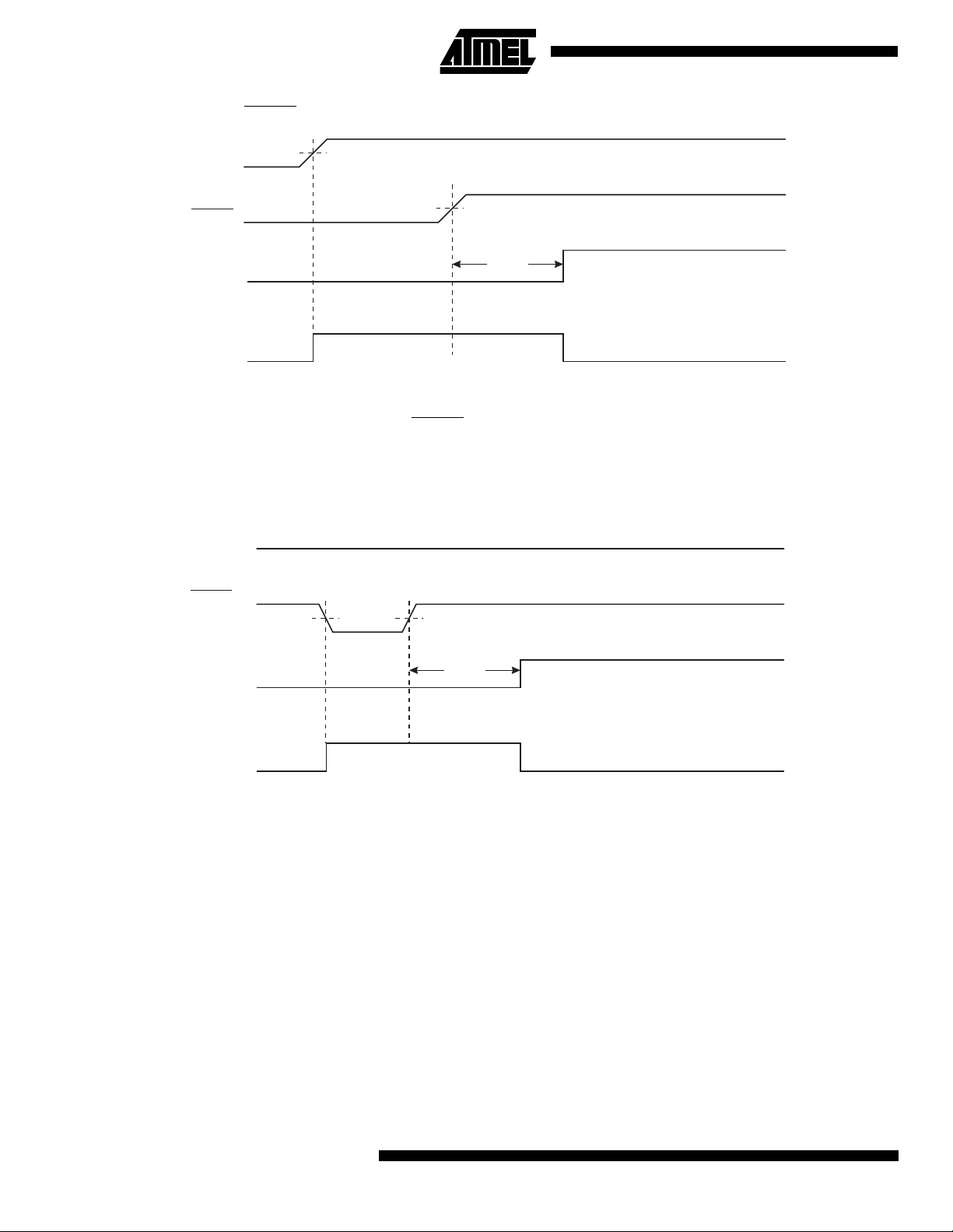
Figure 25. MCU Start-Up, RESET
VCC
RESET
TIME-OUT
INTERNAL
RESET
Controlled Externally
V
POT
V
RST
t
TOUT
External Reset
An external reset is generated by a low level on the RESET
pin. Reset pulses longer than 50 ns will generate a reset, even
if the clock is not running. Shorter pulses are not guaranteed to generate a reset. When the ap plied signal reaches the
Reset Thresh old Vo ltage - V
- on its positive edge, the delay timer starts the MCU after the Time-out period t
RST
TOUT
has
expired.
Figure 26. External Reset During Operation
VCC
RESET
V
RST
t
TIME-OUT
INTERNAL
RESET
TOUT
Watchdog Reset
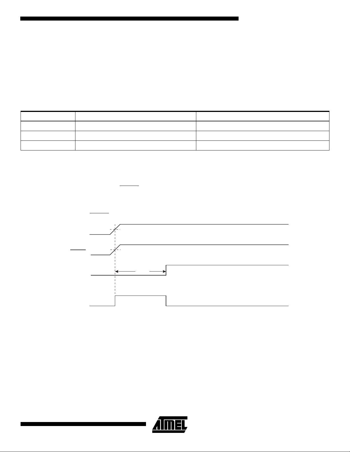
When the Watchdo g tim es out, i t will generate a sh ort rese t pulse o f 1 XT AL cyc le durati on. On the falli ng edge of this
pulse, the delay timer starts counting the Time-out period t
. Refer to page 51 for details on operation of the Watchdog.
TOUT
28
ATmega603/103
Page 29
Figure 27. Watchdog Reset During Operation
VCC
RESET
ATmega603/103
WDT
TIME-OUT
RESET
TIME-OUT
INTERNAL
RESET
1 XTAL Cycle
t
TOUT
MCU Status Register - MCUSR
The MCU Status Register provides information on which reset source caused an MCU reset.
Bit 7 654321 0
$34 ($54) - - - - - - EXTRF PORF MCUSR
Read/WriteR RRRRRR/WR/W
Initial value 0 0 0 0 0 0 See bit description
•
Bits 7..2 - Res: Reserved Bits
These bits are reserved bits in the ATmega603/103 and always read as zero.
Bit 1 - EXTRF: External Reset Flag
•
After a power-on reset, this bit is undefined (X). It will be set by an external reset. A watchdog reset will leave this bit
unchanged.
Bit 0 - PORF: Power-on Reset Flag
•
This bit is set by a power-on reset. A watchdog reset or an external reset will leave this bit unchanged.
To summarize, the following table shows the value of these two bits after the three modes of reset:
Table 8. PORF and EXTRF Values after Reset
Reset Source EXTRF PORF
Power-on Reset undefined 1
External Reset 1 unchanged
Watchdog Reset unchanged unchanged
To make use of these bi ts to ident ify a reset conditio n, the us er softwa re should clear bot h the PORF an d EXTRF bits as
early as possible in the program. Checking the PORF and EXTRF values is done before the bits are cleared. If the bit is
cleared before an external or watchdog reset occurs, the source of reset can be found by using the following truth table:
Table 9. Reset Source Identification
EXTRF PORF Reset Source
0 0 Watchdog Reset
0 1 Power-on Reset
1 0 External Reset
1 1 Power-on Reset
29
Page 30

Interrupt Handling
The ATmega603/103 has two dedicated 8-bit Interrupt Mask control registers; EIMSK - External Interrupt Mask register and
TIMSK - Timer/Counter Interrupt Mask register. In addition, other enable and mask bits can be found in the peripheral
control registers.
When an interrupt occurs, the Global Interrupt Enable I-bit is cleared (zero) and all interrupts are disabled. The user software can set (one) the I-bit to enable nested interrupts. The I-bit is set (one) when a Return from Interrupt instruction - RETI
- is executed.
When the Program Counter is vectored to the actual interrupt vector in order to execute the interrupt handling routine, hard-
ware clears the corresponding flag that generated the interrupt. Some of the interrupt flags can also be cleared by writing a
logic one to the flag bit position(s) to be cleared.
If an interrupt condition occurs when the corresponding interrupt enable bit is cleared (zero), the interrupt flag will be set
and remembered until the interrupt is enabled, or the flag is cleared by software.
If one or more interrupt conditi ons occu r when the global interrupt ena ble bit is clea red (zero), th e correspondi ng interrup t
flag(s) will be set and remembered until the global interrupt enable bit is set (one), and will be executed by order of priority.
Note that external level interrupt does not have a flag, and will only be remembered for as long as the interrupt condition is
active.
Note that the status register is not automatically stored when entering an interrupt routine and restored when returning from
an interrupt routine. This must be handled by software.
External Interrupt Mask Register - EIMSK
Bit 7654 3 2 10
$39 ($59) INT7 INT6 INT5 INT4 INT3 INT2 INT1 INT0 EIMSK
Read/Write R/W R/W R/W R/W R/W R/W R/W R/W
Initial value 0 0 0 0 0 0 0 0
•
Bits 7..4 - INT7 - INT4: External Interrupt Request 7-4 Enable
When an INT7- INT4 bit is set (one) and the I-bit in the Status Register (SREG) is set (one), the corresponding external pin
interrupt is enabled. The Inter rupt Sens e Control bits in th e Externa l Interru pt Contro l Register - EICR defin es whethe r the
external interrupt is acti vated on risi ng or f allin g edge or l evel s ensed . Activ ity on a ny of these pins wi ll trig ger a n inte rrupt
request even if the pin is enabled as an output. This provides a way of generating a software interrupt.
Bits 3..0 - INT3 - INT0: External Interrupt Request 3-0 Enable
•
When an INT3 - INT0 bit is set (one) and the I-bit in the Status Register (SREG) is set (one), the corresponding external pin
interrupt is enabled . The ex tern al in terrupts are al ways lo w lev el trig gered inter rupts. Activi ty on any o f thes e pin s will trigger an interrupt request even if the pin is enabl ed as an output. This p rovides a way of ge nerating a so ftware interru pt.
When enabled, a level triggered interrupt will generate an interrupt request as long as the pin is held low.
External Interrupt Flag Register - EIFR
Bit 7654 3 2 10
$38 ($58) INTF7 INTF6 INTF5 INTF4 - - - - EIFR
Read/Write R/W R/W R/W R/W R R R R
Initial value 0 0 0 0 0 0 0 0
Bits 7..4 - INTF7 - INTF4: External Interrupt 7-4 Flags
•
When an event on the INT7 - INT4 pins triggers an interrupt request, the corresponding interrupt flag, INTF7 - INTF4
becomes set (one). If the I-bit in SREG and the corresponding interrupt enable bit, INT7 - INT4 in EIMSK, are set (one), the
MCU will jump to the interrupt vector. The flag is cleared when the interrupt routine is executed. Alternatively, the flag is
cleared by writing a logical one to it.
Bits 3..0 - Res: Reserved Bits
•
These bits are reserved bits in the ATmega603/103 and always read as zero.
30
ATmega603/103
Page 31

ATmega603/103
External Interrupt Control Register - EICR
Bit 7654 3 2 1 0
$3A ($5A) ISC71 ISC70 ISC61 ISC60 ISC51 ISC50 ISC41 ISC40 EICR
Read/Write R/W R/W R/W R/W R/W R/W R/W R/W
Initial value 0 0 0 0 0 0 0 0
•
Bits 7..0 - ISCX1, ISCX0: External Interrupt 7-4 Sense Control bits
The External Interrupts 7 - 4 a re ac tiva ted by the external pins INT7 - INT4 if the SREG I- fla g an d th e c orr es pon din g i nte rrupt mask in the EIMSK is set. The level and edges on the external pins that activate the interrupts are defined in the
following table:
Table 10. Interrupt Sense Control
ISCX1 ISCX0 Description
0 0 The low level of INTX generates an interrupt request.
01Reserved
1 0 The falling edge of INTX generates an interrupt request.
1 1 The rising edge of INTX generates an interrupt request.
Note: X = 7, 6, 5 or 4.
When changing the ISC X1 /ISCX 0 bit s, the int errup t m us t be di sa ble d b y cle ari ng its Interrupt Enable bit in the GIM SK Re gis ter.
Otherwise an interrupt can occur when the bits are changed.
The value on the INTX pin is sampled before detecting edges. If edge interrupt is selected, pulses that last longer than one
CPU clock period will generate an interrupt. Shorter pulses are not guaranteed to generate an interrupt.
clock frequency c an be lowe r than the X TAL frequency if the XTAL divider is enabled.
If low level inte rrupt i s se lected , the
low level must be held until the completion of the currently executing instruction to generate an interrupt.
Observe that CPU
If enabled, a level
triggered interrupt will generate an interrupt request as long as the pin is held low.
Timer/Counter Interrupt Mask Register - TIMSK
Bit 7 6 5 4 3 2 1 0
$37 ($57) OCIE2 TOIE2 TICIE1 OCIE1A OCIE1B TOIE1 OCIE0 TOIE0 TIMSK
Read/Write R/W R/W R/W R/W R/W R/W R/W R/W
Initial value 0 0 0 0 0 0 0 0
•
Bit 7 - OCIE2: Timer/Counter2 Output Compare Interrupt Enable
When the OCIE2 bit is set (on e) and the I- bi t in the S tatus Reg ister is set ( one ), th e Tim er/Cou nter 2 Co mpa re Match i nte rrupt is enabled. The correspo nding in terrupt ( at vector $0012) is executed i f a Compar e match in Tim er/Cou nter2 oc curs,
i.e., when the OCF2 bit is set in the Timer/Counter Interrupt Flag Register - TIFR.
Bit 6 - TOIE2: Timer/Counter2 Overflow Interrupt Enable
•
When the TOIE2 bit is set (one) and the I-bit in the Status Register is set (one), the Timer/Counter2 Overflow interrupt is
enabled. The corresponding interrup t (at vector $001 4) is exec uted if an over flow in Time r/Coun ter2 occu rs, i.e., when the
TOV2 bit is set in the Timer/Counter Interrupt Flag Register - TIFR.
Bit 5 - TICIE1: Timer/Counter1 Input Capture Interrupt Enable
•
When the TICIE1 bit is set (one) a nd the I-bit in the Statu s Register is set (one), th e Timer/Co unter1 Input Capt ure Event
Interrupt is enabled. The corresponding interrupt (at vector $0016) is executed if a capture-triggering event occurs on pin
29, PD4(IC1), i.e., when the ICF1 bit is set in the Timer/Counter Interrupt Flag Register - TIFR.
Bit 4 - OCE1A: Timer/Counter1 Output CompareA Match Interrupt Enable
•
When the OCIE1A bit is set (one) and the I-bit in the Status Register is set (one), the Timer/Counter1 CompareA Match
interrupt is enabled. The corresponding interrupt (at vector $0018) is executed if a CompareA match i n Timer/Counter1
occurs, i.e., when the OCF1A bit is set in the Timer/Counter Interrupt Flag Register - TIFR.
31
Page 32

•
Bit 3 - OCIE1B: Timer/Counter1 Output CompareB Match Interrupt Enable
When the OCIE1B bit is set (one) and the I-bit in the Status Register is set (one), the Timer/Counter1 CompareB Match
interrupt is enabled. The corresponding interrupt (at vector $001A) is executed if a Compare B match in Timer/Counter1
occurs, i.e., when the OCF1B bit is set in the Timer/Counter Interrupt Flag Register - TIFR.
Bit 2 - TOIE1: Timer/Counter1 Overflow Interrupt Enable
•
When the TOIE1 bit is set (one) and the I-bit in the Status Register is set (one), the Timer/Counter1 Overflow interrupt is
enabled. The correspondin g in ter rupt ( at v ector $001 C) is executed if an overflow in Timer/Cou nter 1 occur s, i.e. , w hen th e
TOV1 bit is set in the Timer/Counter Interrupt Flag Register - TIFR.
Bit 1 - OCIE0: Timer/Counter0 Output Compare Interrupt Enable
•
When the OCIE0 bit is set (on e) and the I- bi t in the S tatus Reg ister is set ( one ), th e Tim er/Cou nter 0 Co mpa re Match i nte r-
rupt is enabled . The corre spon ding in terr upt (a t vec tor $0 01E) is exec uted i f a Compar e m atch in Time r/Coun ter0 occurs ,
i.e., when the OCF0 bit is set in the Timer/Counter Interrupt Flag Register - TIFR.
Bit 0 - TOIE0: Timer/Counter0 Overflow Interrupt Enable
•
When the TOIE0 bit is set (one) and the I-bit in the Status Register is set (one), the Timer/Counter0 Overflow interrupt is
enabled. The corresponding interrup t (at vector $002 0) is exec uted if an over flow in Time r/Coun ter0 occu rs, i.e., when the
TOV0 bit is set in the Timer/Counter Interrupt Flag Register - TIFR
Timer/Counter Interrupt Flag Register - TIFR
Bit 7 6 5 4 3 2 1 0
$36 ($56) OCF2 TOV2 ICF1 OCF1A OCF1B TOV1 OCF0 TOV0 TIFR
Read/Write R/W R/W R/W R/W R/W R/W R/W R/W
Initial value 0 0 0 0 0 0 0 0
Bit 7 - OCF2: Output Compare Flag 2:
•
The OCF2 bit is set (o ne) wh en c om par e m atch o cc urs be tween Tim er /Cou nter 2 and the data in O CR2 - O ut put Comp ar e
Register 2. OCF2 is c le ared by hardware when executi ng the c orr es pon ding i nte rrup t handling vector. Altern ati vely , O CF2
is cleared by writing a l ogic one to the flag. W hen the I-bit in SRE G, and OCIE2 (T imer/Counter2 Compare Interru pt
Enable), and the OCF2 are set (one), the Timer/Counter2 Output Compare Interrupt is executed.
Bit 6 - TOV2: Timer/Counter2 Overflow Flag
•
The TOV2 bit is set (one) when an overflow occurs in Timer/Counter2. TOV2 is cleared by hardware when executing the
corresponding interrupt handling vector. Alternatively, TOV2 is cleared by writing a logic one to the flag. When the I-bit in
SREG, and TOIE2 (T imer/Counter 1 Overflow Inter rupt Enable ), and TOV2 ar e set (one), the Ti mer/Counter 2 Overflow
Interrupt is executed. In PWM mode, this bit is set when Timer/Counter2 advances from $00.
Bit 5 - ICF1: Input Capture Flag 1
•
The ICF1 bit is set (one) to flag an input capture event, indicating that the Timer/Counter1 value has been transferred to the
input capture register - ICR1. ICF1 is cleared by har dware when executi ng the corresp onding interrupt han dling vector.
Alternatively, ICF1 is cleared by writing a logic one to the flag. When the SREG I-bit, and TICIE1 (Timer/Counter1 Input
Capture Interrupt Enable), and ICF1 are set (one), the Timer/Counter1 Capture Interrupt is executed.
Bit 4 - OCF1A: Output Compare Flag 1A
•
The OCF1A bit is set (one) when compare match oc curs between the Time r/Counter1 and the data in OCR1A - Output
Compare Register 1A. OCF1A is cleared by hardware when executing the corresponding interrupt handling vector. Alternatively, OCF1A is cleared by writing a logic one to the flag. When the I-bit in SREG, and OCIE1A (Timer/Counter1 Compare
Interrupt Enable), and the OCF1A are set (one), the Timer/Counter1 Compare A match Interrupt is executed.
Bit 3 - OCF1B: Output Compare Flag 1B
•
The OCF1B bit is set (one) when compare match oc curs between the Time r/Counter1 and the data in OCR1B - Output
Compare Register 1B. OCF1B is cleared by hardware when executing the corresponding interrupt handling vector. Alternatively, OCF1B is cleared by writing a logic one to the flag.. When the I-bit in SREG, and OCIE1B (Timer/Counter1 Compare
match Interrupt Enable), and the OCF1B are set (one), the Timer/Counter1 Compare B match Interrupt is executed.
32
ATmega603/103
Page 33

ATmega603/103
•
Bit 2 - TOV1: Timer/Counter1 Overflow Flag
The TOV1 is set (one) when an overflow occu rs i n Tim er /Co unte r1 . TOV1 is c lea red b y h ar dwa re when ex ec uti ng the co rresponding int errupt hand ling vecto r. Alterna tively, TOV 1 is clear ed by writin g a logic one to th e flag. Whe n the I-bit in
SREG, and TOIE1 (T imer/Counter 1 Overflow Inter rupt Enable ), and TOV1 ar e set (one), the Ti mer/Counter 1 Overflow
Interrupt is executed. In PWM mode, this bit is set when Timer/Counter1 advances from $0000.
Bit 1 - OCF0: Output Compare Flag 0
•
The OCF0 bit is set (o ne) wh en c om par e m atch o cc urs be tween Tim er /Cou nter 0 and the data in O CR0 - O ut put Comp ar e
Register 0. OCF0 is c le ared by hardware when executi ng the c orr es pon ding i nte rrup t handling vector. Altern ati vely , O CF0
is cleared by writing a l ogic one to the flag. W hen the I-bit in SRE G, and OCIE0 (T imer/Counter2 Compare Interru pt
Enable), and the OCF0 are set (one), the Timer/Counter0 Output Compare Interrupt is executed.
Bit 0 - TOV0: Timer/Counter0 Overflow Flag
•
The bit TOV0 is set (one) when an overflow occurs in Timer/Counter0. TOV0 is cleared by hardware when executing the
corresponding interrupt handling vector. Alternatively, TOV0 is cleared by writing a logic one to the flag. When the SREG Ibit, and TOIE0 (Timer/Counter0 Overflow Interrupt Enable), and TOV0 are set (one), the Timer/Counter0 Overflow interrupt
is executed. In PWM mode, this bit is set when Timer/Counter0 advances from $00.
Interrupt Response Time
The interrupt execution res ponse for all the enabl ed AVR interrupts is 4 cloc k cycles minim um. 4 clock cycles after the
interrupt flag h as been set , the pro gram ve ctor addre ss for the actual interru pt handl ing routi ne is exec uted. Du ring this 4
clock cycle period, the Program Counter (2 bytes) is pushed onto the Stack, and the Stack Pointer is decremented by 2.
The vector is nor ma ll y a jum p t o t he interrupt routine, and th is j ump ta kes 3 clock cyc les . If a n i nte rrupt occurs during ex ecution of a multi-cycle instruction, this instruction is completed before the interrupt is served.
A return from an interrupt handling routine (same as for a subroutine call routine) takes 4 clock cycles. During these 4 clock
cycles, the Program Counter (2 bytes) is popped back from the Stack, and the Stack Pointer is incremented by 2. When the
AVR exits from an interrupt, it will always return to the main program and execute one more instruction before any pending
interrupt is served.
Sleep Modes
To enter any of the three sleep modes, the SE bit in MCUCR must be set (one) and a SLEEP instruction must be executed.
The SM1 and SM0 bits in the MCUCR register select which sleep mode (Idle, Power Down, or Power Save) will be activated by the SLEEP instruction, see Table 4.
If an enabled interrup t occurs while the MCU is in a sleep mod e, the MCU awakes , executes the i nterrupt rout ine, and
resumes execution from the instruction following SLEEP. The contents of the register file, SRAM, and I/O memory are unaltered. If a reset occurs during sleep mode, the MCU wakes up and executes from the Reset vector
Idle Mode
When the SM1/SM0 bits are set to 00, the SLEEP i nstructi on makes the MCU enter th e Idle Mode, sto pping the CPU but
allowing SPI, UART, Analog Comparator, ADC, Timer/Counters, Watchdog and the interrupt system to continue operating.
This enables the MCU to wake up from external triggered interrupts as well as internal ones like the Timer Overflow and
UART Receive Complete interrupts. If wake-up from the Analog Comparator interrupt is not required, the analog comparator can be powered down by setting the ACD-bit in the Analog Comparator Control and Status register - ACSR. This will
reduce power co nsumption in Id le Mode. When t he MCU wa kes up from Idle mode , the CPU starts p rogram e xecution
immediately.
33
Page 34

Power Down Mode
When the SM1/SM0 bit s are set to 10, the S LEEP in struct ion mak es the M CU enter the P ower Do wn Mode. In this mod e,
the external oscillator is stopped, while the external interrupts and the Watchdog (if enabled) continue operating. Only an
external reset, a watchdog reset (if enabled), or an external level interrupt can wake up the MCU.
Note that if a level triggered interrupt is used fo r wake-up from P ower Down Mode, the changed level mu st be held for
some time to wake up the MCU. This makes the MCU le ss sensi tive to noi se. The c hanged level is sampled twi ce by the
watchdog oscillator cl ock, a nd if the inp ut ha s the requi red level d uring this time , the MCU wi ll wa ke u p. The period of th e
watchdog oscillator is 1 us (nominal) at 5.0V and 25C. The frequency of the watchdog oscillator is voltage dependent as
shown in section “Typical char acteristics” on page 110.
When waking up from Powe r Down Mode, ther e is a delay fro m the wake-up conditio n occurs un til the wake-u p becomes
effective. This a llows the clo ck to res tart a nd bec ome stab le aft er ha ving been s topped . The wak e-up pe riod is defi ned by
the same SUT fuses that define the r ese t tim e-out period. The wake-up period is equa l to the cl ock re se t per iod, as sho wn
in Table 6.
If the wake-up condition disappears before the MCU wakes up and starts to execute, e.g. a low level on is not held long
enough, the interrupt causing the wake-up will not be executed.
Power Save Mode
When the SM1/SM0 bits are 11, the SLEEP instruction makes the MCU enter the Power Save Mode. This mode is identical
to Power Down, with one exception:
If Timer/Counter0 is clocked as y nch ronou sl y , i.e. th e AS 0 bi t in ASS R is s et, Tim er/Co unte r0 will run dur in g sl ee p. In add ition to the Power Down wa ke-up s ources, the device ca n also wa ke up fro m either Time r Overflow o r Output Compare
event from Timer/Counter0 i f the corr espon ding Tim er/Counter 0 interr upt enab le bits ar e set in TIMSK. To en sure that th e
part executes the Interrupt routine when waking up, also set the global interrupt enable bit in SREG.
When waking up from Power Save Mode by an exter nal interrupt, 2 i nstruction cy cles are exec uted before the inte rrupt
flags are updated. When waking up by the asynchronous timer, 3 instruction cycles are executed before the flags are
updated. During these cycles, the processor executes instructions, but the interrupt condition is not readable, and the
interrupt routine has not started yet .
Timer/Counters
The ATmega603/103 pr ovid es th re e g ene ral purpose Timer/Counter s - t wo 8-bit T/Cs and one 16 -b it T/C. Ti me r/C ount er 0
can optionally be asynchronously clocked from an external oscillator. This oscillator is optimized for use with a 32.768 kHz
crystal, enabling use of Timer/Counter0 as a Real Time Clock (RTC). Timer/Counter0 has its own prescaler.
Timer/Counters 1 and 2 have ind ivid ual pres caling se lecti on from the same 10- bit pres cali ng timer. Thes e Timer/Co unters
can either be used as a timer with an internal clock timebase or as a counter with an external pin connection which triggers
the count ing.
34
ATmega603/103
Page 35

Timer/Counter Prescalers
Figure 28. Prescaler for Timer/Counter 1 and Timer/Counter2
ATmega603/103
CK
T1
T2
CS20
CS21
CS22
0
TIMER/COUNTER2 CLOCK SOURCE
TCK2
10-BIT T/C PRESCALER
CK/8
CS10
CS11
CS12
CK/64
CK/256
0
TIMER/COUNTER1 CLOCK SOURCE
CK/1024
TCK1
For Timer/Counters 1 and 2, the four different prescaled selections are: CK/8, CK/64, CK/256 and CK/1024 where CK is
the CPU clock. Observe that CPU clock frequency can be lower than the XTAL frequency if the XTAL divider is enabled. For
Timer/Counters 1 and 2, added selections as CK, external source and stop, can be selected as clock sources.
Figure 29. The Timer/Counter0 Prescaler
CK
TOSC1
AS0
CS00
CS01
CS02
PCK0
10-BIT T/C PRESCALER
PCK0/8
TIMER/COUNTER0 CLOCK SOURCE
PCK0
PCK0/32
PCK0/64
PCK0/128
PCK0/256
PCK0/1024
35
Page 36
The clock source for Timer/Counter0 prescaler is named PCK0. PCK0 is by default connected to the main system clock
CK. Observe that CPU clock frequency can be lower than the XTAL frequency if the XTAL divider is enabled. By setting the
AS0 bit in ASSR , Timer/Counter 0 p rescaler is asy nchronously clo cked from the TOS C1 pin. This en ables use of
Timer/Counter0 as a Real Time Clock (RTC). A crystal can be connected between the TOSC1 and TOSC2 pins to serve as
an independent clock source for Timer/Counter0. This oscillator is optimized for use with a 32.768 kHz crystal.
8-bit Timer/Counters T/C0 and T/C2
Figure 30 shows the block diagram for Timer/Counter0.
Figure 30. Timer/Counter0 Block Diagram
8-BIT DATA BUS
8-BIT ASYNCH T/C0 DATA BUS
OCIE1B
TOIE2
TICIE1
OCIE1A
OCIE2
TIMER INT. MASK
REGISTER (TIMSK)
7
TIMER/COUNTER0
(TCNT0)
7
8-BIT COMPARATOR
7
OUTPUT COMPARE
REGISTER0 (OCR0)
TOIE1
OCIE0
TOIE0
0
0
0
TCK0
CK
T/C0 OVER-
FLOW IRQ
TIMER INT. FLAG
REGISTER (TIFR)
TOV2
OCF2
T/C CLEAR
T/C CLK SOURCE
UP/DOWN
T/C0 COMPARE
MATCH IRQ
ICF1
OCF2B
OCF2A
SYNCH UNIT
OCF0
TOV0
T/C0 CONTROL
REGISTER (TCCR0)
CS02
CS01
CS00
CTC0
PWM0
COM01
TOV0
TOV1
OCF0
CONTROL
LOGIC
COM00
ASYNCH. STATUS
REGISTER (ASSR)
AS0
TC0UB
OCR0UB
PCK0
ICR0UB
36
ATmega603/103
Page 37
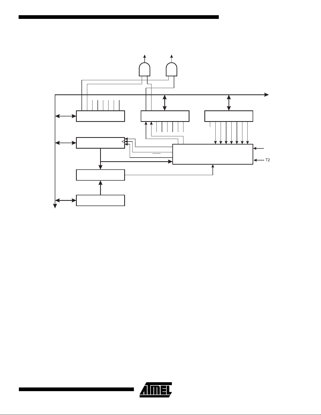
Figure 31. Timer/Counter2 Block Diagram
OCIE1B
TICIE1
(TCNT2)
OCIE1A
TOIE1
OCIE0
OCIE2
TOIE2
TIMER INT. MASK
REGISTER (TIMSK)
8-BIT DATA BUS
7
TIMER/COUNTER2
7
8-BIT COMPARATOR
TOIE0
0
0
T/C2 OVER-
FLOW IRQ
OCF2
TOV2
TIMER INT. FLAG
REGISTER (TIFR)
TOV2
OCF2
T/C CLEAR
T/C CLK SOURCE
UP/DOWN
T/C2 COMPARE
MATCH IRQ
ICF1
OCF2B
OCF2A
TOV1
OCF0
ATmega603/103
T/C2 CONTROL
REGISTER (TCCR2)
CS21
CS20
CS22
COM20
COM21
CTC2
CK
T2
TOV0
PWM2
CONTROL
LOGIC
7
OUTPUT COMPARE
REGISTER2 (OCR2)
0
Note: Figure 31 shows the block diagram for Timer/Counter2.
The 8-bit Timer/Cou nter0 can sele ct clock sourc e from PCK0 or pres caled PCK0 . The 8-bit Timer /Counter2 can s elect
clock source from CK, prescaled CK, or an external pin. Both Timer/Counters can be stopped as described in the specification for the Timer/Counter Control Registers - TCCR0 and TCCR2.
The different status flags (overflow, compare match and capture event) are found in the Timer/Counter Interrupt Flag Register - TIFR. Control signals are found in the Timer/Counter Control Registers - TCCR0 and TCCR2. The interrupt
enable/disable settings are found in the Timer/Counter Interrupt Mask Register - TIMSK.
When Timer/Counter2 is externally clocked, the external signal is synchronized with the oscillator frequency of the CPU. To
assure proper sampling of the external clock, the minimum time between two external clock transitions must be at least one
internal CPU clock period. The external clock signal is sampled on the rising edge of the internal CPU clock.
The 8-bit Timer/Counters feature a high resolution and a high accuracy usage with the lower prescaling opportunities. Similarly, the high prescaling opportunities m ake these un its useful for lower speed function s or exact ti ming functions wi th
infrequent actions.
Both Timer/Counters support two Output Compare functions using the Output Compare Registers - OCR0 and OCR2 as
the data source to be compared to the Timer/Counter contents. The Output Compare functions include optional clearing of
the counter on compare match, and action on the O utput Compare Pins - PB4( OC0/PWM0) and PB7(OC2/PW M2) - on
compare match.
Timer/Counter0 and 2 can also be used as 8-bit Pulse Width Modulators. In this mode the Timer/Counter and the output
compare register serve as a glitch-free, stand-alone PWM with centered pulses. Refer to page 40 for a detailed description
on this function.
37
Page 38
Timer/Counter0 Control Register - TCCR0
Bit 7 6 5 4 3 2 1 0
33 ($53) - PWM0 COM01 COM00 CTC0 CS02 CS01 CS00 TCCR0
Read/Write R R/W R/W R/W R/W R/W R/W R/W
Initial value 0 0 0 0 0 0 0 0
Timer/Counter2 Control Register - TCCR2
Bit 7 6 5 4 3 2 1 0
$25 ($45) - PWM2 COM21 COM20 CTC2 CS22 CS21 CS20 TCCR2
Read/Write R R/W R/W R/W R/W R/W R/W R/W
Initial value 0 0 0 0 0 0 0 0
•
Bit 7 - Res: Reserved Bit
This bit is a reserved bit in the ATmega603/103 and always reads as zero.
Bit 6 - PWM0 / PWM2: Pulse Width Modulator Enable
•
When set (one) this bit enables PWM mode for Timer/Counter0 or Timer/Counter2. This mode is described on page 40.
Bits 5,4 - COM01, COM00 / COM21, COM20: Compare Output Mode, bits 1 and 0
•
The COMn1 and COMn0 control bi ts determine any outpu t pin action follo wing a compare match in Timer/Counter2.
Any output pin actions affec t pins PB4(OC0/P WM0) or PB7(OC2/P WM2). Si nce this i s an al ternative function to an I/O
port, the corresponding direction control bit must be set (one) to control an output pin. The control configuration is shown in
Table 11.
Table 11. Com par e Mod e Sele ct
COMn1 COMn0 Description
0 0 Timer/Counter disconnected from output pin OCn/PWMn
0 1 Toggle the OCn/PWMn output line.
1 0 Clear the OCn/PWMn output line (to zero).
1 1 Set the OCn/PWMn output line (to one).
Note: n = 0 or 2
In PWM mode, these bits have a different function. Refer to Table 14 for a detailed description.
• Bit 3 - CTC0 / CTC2: Clear Timer/Counter on Compare match
When the CTC0 or CTC2 c ont ro l b it is se t ( one ), the Tim er /Cou nter i s re se t to $00 in the CPU clock cycle afte r a c omp ar e
match. If the control bit is cleared, the Timer continues counting and is unaffected by a compare match. Since the compare
match is detected in the CPU clock cycle following the match, this function will behave differently when a prescaling higher
than 1 is used for the timer. When a prescaling of 1 is used, and the compare register is set to C, the timer will count as follows if CTC0/2 is set:
... | C-2 | C-1 | C | 0 | 1 | ...
When the prescaler is set to divide by 8, the timer will count like this:
... | C-2, C-2, C-2, C-2, C-2, C-2, C-2, C-2 | C-1, C-1, C-1, C-1, C-1, C-1, C-1, C-1 | C, 0, 0, 0, 0, 0, 0, 0, 0 | 1, 1, 1, ...
In PWM mode, this bit has no effect.
Bits 2,1,0 - CS02, CS01, CS00 / CS22, CS21, CS20: Clock Select bits 2,1 and 0
•
The Clock Select2 bits 2,1 and 0 define the prescaling source of the Timer/Counter.
38
ATmega603/103
Page 39

Table 12. Timer/Counter0 Prescale Select
CS02 CS01 CS00 Description
0 0 0 Timer/Counter0 is stopped.
001PCK0
010PCK0/8
011PCK0/32
100PCK0/64
1 0 1 PCK0/128
1 1 0 PCK0/256
1 1 1 PCK0/1024
Table 13. Timer/Counter2 Prescale Select
CS22 CS21 CS20 Description
0 0 0 Timer/Counter2 is stopped.
001CK
ATmega603/103
0 1 0 CK/8
011CK/64
1 0 0 CK/256
1 0 1 CK/1024
1 1 0 External Pin PD7(T2), falling edge
1 1 1 External Pin PD7(T2), rising edge
The Stop condition provides a Timer Enable/Disable function. The CK down divided modes are scaled directly from the CK
CPU clock. If the external pin modes are used for Timer/Counter2, transitions on PD7/(T2) will clock the counter even if the
pin is configured as an output. This feature can give the user SW control of the counting.
Timer/Counter0 - TCNT0
Bit 76543210
$32 ($42) M SB LSB TCNT0
Read/Write R/W R/W R/W R/W R/W R/W R/W R/W
Initial value00000000
Timer/Counter2 - TCNT2
Bit 76543210
$24 ($44) M SB LSB TCNT2
Read/Write R/W R/W R/W R/W R/W R/W R/W R/W
Initial value00000000
These 8-bit registers contains the value of the Timer/Counters.
Both Timer/Counters are realized as up or up/down (in PWM mode) counters with read and wr ite access. If the
Timer/Counter is written to and a clock source is selected, it continues counting in the timer clock cycle after it is preset with
the written value.
39
Page 40

Timer/Counter0 Output Compare Register - OCR0
Bit 76543210
$31 ($51) MSB LSB OCR0
Read/Write R/W R/W R/W R/W R/W R/W R/W R/W
Initial value00000000
Timer/Counter2 Output Compare Register - OCR2
Bit 76543210
$23 ($43) MSB LSB OCR2
Read/Write R/W R/W R/W R/W R/W R/W R/W R/W
Initial value00000000
The output compare registers are 8-bit read/write registers.
The Timer/Counter Output Compare Registers contain the data to be continuously compared with the Timer/Counter.
Actions on compare matches a re sp ecifi ed i n TCCR0 and TCCR2. A compare match does on ly occu r if the Tim er/Coun ter
counts to the OCR value. A software write that sets the Timer/Counter and Output Compare Register to the same value
does not generate a compare match.
A compare match will set the compare interrupt flag in the CPU clock cycle following the compare event.
Timer/Counter 0 and 2 in PWM mode
When the PWM mode is selected, the Timer/Counter and the Output Compare Register - OCR0 or OCR2 form an 8-bit,
free-running, glitch-free and phase correct PWM with outputs on the PB4(OC0/PWM0) or PB7(OC2/PW M2) pin. The
Timer/Counter acts as an up/down counter, counting up from $00 to $FF, where it turns and counts down again to zer o
before the cycle is repeated. When the counter value matches the contents of the Output Compare register, the
PB4(OC0/PWM0) or PB7(OC2/PWM2) pin is set or cleared according to the settings of the COM01/COM00 or
COM21/COM20 bits in the Timer/Counter Control Registers TCCR0 and TCCR2. Refer to Table 14 for details.
Table 14. Compare Mode Select in PWM Mode
COMn1 COMn0 Effect on Compare/PWM Pin
0 0 Not connected
0 1 Not connected
10
1 1 Cleared on compar e match, down -counting. Set on compare match, up-counting (inverted PWM).
Note: n = 0 or 2
Cleared on compare match, up-counting. Set on compare match, down-counting (non-inverted
PWM).
Note that in PWM mode, the Output Compare regis ter is transfe rred to a tem porary locatio n when writte n. The value is
latched when the Timer/Counter reaches $FF. This prevents the occurrence of odd-length PWM pulses (glitches) in the
event of an unsynchronized OCR0 or OCR2 write. See Figure 32 for an example.
40
ATmega603/103
Page 41

ATmega603/103
Figure 32. Effects on Unsynchron iz ed OCR Latching
Compare Value changes
Counter Value
Compare Value
PWM Output
Synchronized OCR Latch
Compare Value changes
Counter Value
Compare Value
PWM Output
Unsynchronized OCR Latch
During the time between the write and the latch operation, a read from OCR0 or OCR2 will read the contents of the temporary location. This means that the most recently written value always will read out of OCR0/2
When the OCR register (not the temporar y register) is up dated to $00 or $FF , the PWM outpu t changes to low or high
immediately according to the settings of COM21/COM20 or COM11/COM10. This is shown in Table 15:
Glitch
Table 15. PWM Outputs OCRn = $00 or $FF
COMn1 COMn0 OCRn Output PWMn
1 0 $00 L
10$FF H
1 1 $00 H
11$FF L
Note: n = 0 or 2
In PWM mode, the Timer Overflow Flag, TOV0 or TOV2, is set when the counter advances from $00. Timer Overflow
Interrupt0 and 2 operates exactly as in normal Timer/Counter mode, i.e. it is executed when TOV0 or TOV2 is set provided
that Timer Overflow Interrupt and global interrupts are enabled. This does also apply to the Timer Output Compare flags
and interrupts.
The frequency of the PWM will be Timer Clock Frequency divided by 510.
Asynchronous Status Register - ASSR
Bit 76543 2 1 0
$30 ($50) - - - - AS0 TCN0UB OCR0UB TCR0UB ASSR
Read/Write R R R R R/W R R R
Initial value 0 0 0 0 0 0 0 0
Bit 7..4 - Res: Reserved Bits
•
These bits are reserved bits in the ATmega603/103 and always reads as zero.
Bit 3 - AS0: Asynchronous Timer/Counter0
•
When set(one) Timer/Counter0 is clocked from the TOSC1 pin. When cleared (zero) Timer/Counter0 is clocked from the
internal system clock, CK. When the value of this bit is changed the contents of TCNT0 might get corrupted.
Bit 2 - TCN0UB: Timer/Counter0 Update Busy
•
When Timer/Counter0 operates asynchronously and TCNT0 is written, this bit becomes set (one). When TCNT0 has been
updated from the te mpora ry stor age regis ter, th is bit is cl eared ( zero) by ha rdwar e. A logic al zero in this bit indicat es that
TCNT0 is ready to be updated with a new value.
41
Page 42

•
Bit 1 - OCR0UB: Output Compare Register0 Update Busy
When Timer/Counter0 operates asynchronously and OCR0 is written, this bit becomes set (one). When OCR0 has been
updated from the te mpora ry stor age regis ter, th is bit is cl eared ( zero) by ha rdwar e. A logic al zero in this bit indicat es that
OCR0 is ready to be updated with a new value.
Bit 0 - TCR0UB: Timer/Counter Control Register0 Update Busy
•
When Timer/Counter0 operates asynchronously and TCCR0 is written, this bit becomes set (one). When TCCR0 has been
updated from the te mpora ry stor age regis ter, th is bit is cl eared ( zero) by ha rdwar e. A logic al zero in this bit indicat es that
TCCR0 is ready to be updated with a new value.
If a write is performed to any of the three Timer/Counter0 registers while its update busy flag is set (one), the updated value
might get corrupted and cause an unintentional interrupt to occur.
When reading TCNT0, OCR0 and TCCR0, there is a difference in result. When reading TCNT0, the actual timer value is
read. When reading OCR0 or TCCR0, the value in the temporary storage register is read.
Asynchronous Operation of Timer/Counter0
When Timer/Counter0 operates synchronously, all operations and timing are identical to Timer/Counter2. During asynchronous operation, however, some considerations must be taken.
• WARNING: When switching between asynchronous and synchronous clocking of Timer/Counter0, the timer registers,
TCNT0, OCR0 and TCCR0 might get corrupted. Safe procedure for switching clock source:
1. Disable the timer 0 interrupts OCIE0 and TOIE0.
2. Select clock source by setting ASO as appropriate.
3. Write new values to TCNT0, OCR0 and TCCR0.
4. If switching to asynchronous operation: Wait for TCNT0UB, OCR0UB and TCR0UB to be cleared.
5. Enable interrupts if needed.
• The oscillator is optimized for use with a 32,768Hz watch crystal. An external clock signal applied to this pin goes
through the same amplifier having a bandwidth of 256kHz. The external clock signal should therefore be in the interval
0Hz - 256kHz. The frequency of the clock signal applied to the TOSC1 pin must be lower than one fourth of the CPU
main clock frequency. Observe that CPU clock frequency can be lower than the XTAL frequency if the XTAL divider is
enabled.
• When writing to one of the registers TCNT0, OCR0, or TCCR0, the value is transferred to a temporary register, and
latched after two positive edges on TOSC1. The user should not write a new value before the contents of the temporary
register have been transferred to its destination. Each of the three mentioned registers have their individual temporary
register, which means that e.g. writing to TCNT0 does not disturb an OCR0 write in progress. To detect that a transfer to
the destination register has taken place, a Asynchronous Status Register - ASSR has been implemented.
• When entering Power Save mode after having written to TCNT0, OCR0 or TCCR0, the user must wait until the written
register has been updated if Timer/Counter0 is used to wake up the device. Otherwise, the MCU will go to sleep before
the changes have had any effect. This is extremely important if the output compare0 interrupt is used to wake up the
device; Output compare is disabled during write to OCR0 or TCNT0. If the write cycle is not finished (i.e. the user goes to
sleep before the OCR0UB bit returns to zero), the device will never get a compare match and the MCU will not wake up.
• If Timer/Counter0 is used to wake up the device from Power Save mode, precautions must be taken if the user wants to
re-enter Power Save mode; The interrupt logic needs one TOSC1 cycle to get reset. If the time between wake up and reentering Power Save mode is less than one TOSC1 cycle, the interrupt will not occur and the device will fail to wake up. If
the user is in doubt whether the time before re-entering Power Save is sufficient, the following algorithm can be used to
ensure that one TOSC1 cycle has elapsed:
1. Write a value to TCCR0, TCNT0 or OCR0
2. Wait until the corresponding Update Busy flag in ASSR returns to zero.
3. Enter Power Save mode
• When asynchronous operation is selected, the 32 kHz oscillator for Timer/Counter0 is always running, except in power
down mode. After a power up reset or wake-up from power down, the user should be aware of the fact that this oscillator
might take as long as one second to stabilize. Therefore, the content of all Timer/Counter0 registers must be considered
42
ATmega603/103
Page 43

ATmega603/103
lost after a wake-up from power down, due to the unstable clock signal. The user is advised to wait for at least one
second before using Timer/Counter0 after power-up or wake-up from power down.
• Description of wake up from power save mode when the timer is clocked asynchronously: When the interrupt condition is
met, the wake up process is started on the following cycle of the timer clock, that is, the timer is always advanced by at
least one before the processor can read the counter value. To execute the corresponding Timer/Counter0 interrupt
routine, the global interrupt bit in SREG must have been set. Otherwise, the part will still wake up from power down, but
continues to execute the sleep command. The interrupt flags are updated 3 processor cycles after the processor clock
has started. During these cycles, the processor executes instructions, but the interrupt condition is not readable, and the
interrupt routine has not started yet.
• During asynchronous operation, the synchronization of the interrupt flags for the asynchronous timer takes 3 processor
cycles plus one timer cycle. The timer is therefore advanced by at least one before the processor can read the timer
value causing the setting of the interrupt flag. The output compare pin is changed on the timer clock, and is not
synchronized to the processor clock.
16-bit Timer/Counter1
Figure 33 shows the block diagram for Timer/Counter1.
The 16-bit Timer/Counter1 can select clock source from CK, prescaled CK, or an external pin. In addition it can be stopped
as described in the specification for the Timer/Counter1 Control Register - TCCR1B. The different status flags (overflow,
compare match and capture event) are found in the Timer/Counter Interrupt Flag Register - TIFR. Control signals are found
in the Timer/Counter1 Control Registers - TCCR1A and TCCR1B. The interrupt enable/disable settings for Timer/Counter1
are found in the Timer/Counter Interrupt Mask Register - TIMSK.
When Timer/Counter1 is externally clocked, the external signal is synchronized with the oscillator frequency of the CPU. To
assure proper sampling of the external clock, the minimum time between two external clock transitions must be at least one
internal CPU clock period. The external clock signal is sampled on the rising edge of the internal CPU clock.
The 16-bit Timer/Counter1 feat ures both a high re solut ion and a high accu racy usage w ith the lower presca ling op portun ities. Similarly, the high prescaling opportunities makes the Timer/Counter1 useful for lower speed functions or exact timing
functions with infrequent actions.
The Timer/Counter1 sup ports two O utpu t Com par e func tions u si ng the Ou tput Com par e R egi st er 1 A an d B - O CR1A an d
OCR1B as the data sources to be compared to the Timer/Counter1 contents. The Output Compare functions include
optional clearing of the counter on compareA match, and actions on the Output Compare pins on both compare matches.
43
Page 44

Figure 33. Timer/Counter1 Block Diagram
K
OCIE0
TOIE0
T/C1 COMPARE
7
8
T/C1 OVER-
FLOW IRQ
OCIE2
TOIE2
TICIE1
OCIE1B
OCIE1A
TOIE1
TIMER INT. MASK
REGISTER (TIMSK)
8-BIT DATA BUS
15
T/C1 INPUT CAPTURE REGISTER (ICR1)
MATCHA IRQ
ICF1
OCF1B
OCF2
TOV2
TIMER INT. FLAG
REGISTER (TIFR)
OCF1B
ICF1
T/C1 COMPARE
MATCHB IRQ
OCF0
TOV0
OCF1A
TOV1
TOV1
OCF1A
CAPTURE
TRIGGER
T/C1 INPUT
CAPTURE IRQ
T/C1 CONTROL
REGISTER A (TCCR1A)
COM1A1
COM1B1
COM1A0
0
COM1B0
PWM11
PWM10
T/C1 CONTROL
REGISTER B (TCCR1B)
ICNC1
ICES1
CONTROL
LOGIC
CTC1
CS12
CS11
CS10
C
T1
15
7
8
TIMER/COUNTER1 (TCNT1)
7
15
8
16 BIT COMPARATOR
7
15
8
TIMER/COUNTER1 OUTPUT COMPARE REGISTER A
0
T/C CLEAR
T/C CLOCK SOURCE
UP/DOWN
7
15
0
8
16 BIT COMPARATOR
7
15
0
8
TIMER/COUNTER1 OUTPUT COMPARE REGISTER B
0
0
Timer/Counter1 can also be used as a 8, 9 or 10-bi t Pulse With Modulator. In this mode the counter and the
OCR1A/OCR1B register s serve as a dual glitch-fr ee stand-alone PWM wi th centered pulses. Ref er to page 49 for a
detailed description on this function.
The Input Capture function of Timer/Counter1 provides a capture of the Timer/Counter1 contents to the Input Capture
Register - ICR1, triggered by an external event on the Input Capture Pi n - PD4/(IC1). The actual capture event settings
are defined by the Timer/Counter1 Control Register - TCCR1B. In addition, the Analog Comparator can be set to trigger
the Input Capture. Refer to the par agraph, “The Anal og Comparator” , for details on this. T he ICP pin logic i s shown
in Figure 34.
Figure 34. ICP Pin Schematic Diagram
44
ATmega603/103
Page 45

ATmega603/103
If the noise canceler function is enabled, the actual trigger condition for the capture event is monitored over 4 samples, and
all 4 must be equal to activate the capture flag.
Timer/Counter1 Control Register A - TCCR1A
Bit 7 6 5 4 3 2 1 0
$2F ($4F) COM1A1 COM1A0 COM1B1 COM1B0 - - PWM11 PWM10 TCCR1A
Read/Write R/W R/W R/W R/W R R R/W R/W
Initial value 0 0 0 0 0 0 0 0
•
Bits 7..6 - COM1A1, COM1A0: Compare Output Mode1A, bits 1 and 0
The COM1A1 and COM1A0 control bits determine any output pi n action following a c ompare match in T imer/Counter1.
Any output pin actions affect pin OC1A - Output CompareA pin 1. This is an alternative function to an I/O port, and the corresponding direction control bit must be set (one) to control an output pin. The control configuration is shown in Table 16..
Bits 5..4 - COM1B1, COM1B0: Compare Output Mode1B, bits 1 and 0
•
The COM1B1 and COM1B0 control bits determine any output pi n action following a c ompare match in T imer/Counter1.
Any output pin actions affect pin OC1B - Output CompareB. Since this is an alternative function to an I/O port, the corresponding direction control bit must be set (one) to control an output pin. The following control configuration is given:
Table 16. Compare 1 Mode Select
COM1X1 COM1X0 Description
0 0 Timer/Counter1 d isconnected from output pin OC1X
0 1 Toggle the OC1X output line.
1 0 Clear the OC1X output line (to zero).
1 1 Set the OC1X output line (to one).
Note: X = A or B.
In PWM mode, these bits have a different function. Refer to Table 17 for a detailed description.
• Bits 3..2 - Res: Reserved bits
These bits are reserved bits in the ATmega603/103 and always read zero.
Bits 1..0 - PWM11, PWM10: Pulse Width Modulator Select Bits
•
These bits select PWM operation of Timer/Counter1 as specified in Table 19. This mode is described on page 49.
Table 17. PWM Mode Select
PWM11 PWM10 Description
0 0 PWM operation of Timer/Counter1 is disabled
0 1 Timer/Counter1 is an 8-bit PWM
1 0 Timer/Counter1 is a 9-bit PWM
1 1 Timer/Counter1 is a 10-bit PWM
45
Page 46

Timer/Counter1 Control Register B - TCCR1B
Bit 7 6 5 4 3 2 1 0
$2E ($4E) ICNC1 ICES1 - - CTC1 CS12 CS11 CS10 TCCR1B
Read/Write R/W R/W R R R/W R/W R/W R/W
Initial value 0 0 0 0 0 0 0 0
•
Bit 7 - ICNC1: Input Capture1 Noise Canceler (4 CKs)
When the ICNC1 bit is cleared (zero), the input capture trigger noise canceler function is disabled. The input capture is triggered at the first rising/fall ing edge sampled o n the input capture pin PD4(IC1) as specifi ed. When t he ICNC1 bit is set
(one), four succ essive samp les are measures on PD4(I C1), and al l sampl es mus t be high/l ow accord ing to th e input capture trigger specification in the ICES1 bit. The actual sampling frequency is XTAL clock frequency.
Bit 6 - ICES1: Input Capture1 Edge Select
•
While the ICES1 bit is cleared (zero), the Timer/Counter1 contents are transferred to the Input Capture Register - ICR1 - on
the falling edge of the input capture pin - PD4(IC1). While the ICES1 bit is set (one), the Timer/Counter1 contents are transferred to the Input Capture Register - ICR1 - on the rising edge of the input capture pin - PD4(IC1).
Bits 5, 4 - Res: Reserved bits
•
These bits are reserved bits in the ATmega603/103 and always read zero.
Bit 3 - CTC1: Clear Timer/Counter1 on Compare Match
•
When the CTC1 control bit is s et (on e) , th e Ti mer /Co unte r1 i s res et to $ 000 0 i n th e c lo ck c y cle a fter a co mpa re A match. If
the CTC1 control bit is cleared, Timer/Counter1 continues counting and is unaffected by a compare match. Since the compare match is detected in the CPU clock cycle following the match, this function will behave differently when a prescaling
higher than 1 is used for the timer. When a prescaling of 1 is used, and the c ompareA register is set to C, the timer will
count as follows i CTC1 is set:
... | C-2 | C-1 | C | 0 | 1 | ...
When the prescaler is set to divide by 8, the timer will count like this:
... | C-2, C-2, C-2, C-2, C-2, C-2, C-2, C-2 | C-1, C-1, C-1, C-1, C-1, C-1, C-1, C-1 | C, 0, 0, 0, 0, 0, 0, 0 | ...
In PWM mode, this bit has no effect.
Bits 2,1,0 - CS12, CS11, CS10: Clock Select1, bit 2,1 and 0
•
The lock Select1 bits 2,1 and 0 define the prescaling source of Timer/Counter1.
Table 18. Clock 1 Prescale Select
CS12 CS11 CS10 Description
0 0 0 Stop, the Timer/Counter1 is stopped.
001CK
010CK/8
011CK/64
100CK/256
101CK/1024
1 1 0 External Pin T1, falling edge
1 1 1 External Pin T1, rising edge
The Stop condition provides a Timer Enable/Disable function. The CK down divided modes are scaled directly from the CK
CPU clock. If the external pin modes are used for Timer/Counter1, transitions on PD6/(T1) will clock the counter even if the
pin is configured as an output. This feature can give the user SW control of the counting.
46
ATmega603/103
Page 47

ATmega603/103
Timer/Counter1 - TCNT1H and TCNT1L
Bit 151413121110 9 8
$2D ($4D) MSB TCNT1H
$2C ($4C) LSB TCNT1L
76543210
Read/Write R/W R/W R/W R/W R/W R/W R/W R/W
R/W R/W R/W R/W R/W R/W R/W R/W
Initial value00000000
00000000
This 16-bit register contain s the prescaled v alue of the 16-b it Timer/Counte r1. To ensure t hat both the high and low by tes
are read and written sim ultane ously w hen the CP U acce sses these regis ters, the ac cess is pe rfor med u sing an 8-bit t emporary register (TEMP). This temporary register is also used when accessing OCR1A, OCR1B and ICR1. If the main
program and also interrupt routines perform access to registers using TEMP, interrupts must be disabl ed during access
from the main program (and from interrupt routines if interrupts are allowed from within interrupt routines).
• TCNT1 Timer/Counter1 Write:
When the CPU writes to the high byte TCNT1H, the wri tten data is pl aced in the TEMP r egister. Next , when the CPU
writes the low byte TCNT1 L, th is byte of data is combi ned with the byte data in the TEMP regi ster, and all 16 bi ts ar e
written to the TCNT1 Timer/Counter1 register simultaneously. Consequently, the high byte TCNT1H must be accessed
first for a full 16-bit register write operation. When using Timer/Counter1 as an 8-bit timer, it is sufficient to write the low
byte only.
• TCNT1 Timer/Counter1 Read:
When the CPU reads the low byte TCNT1L, the data of TCNT1L is sent to the CPU and the data of the high byte
TCNT1H is placed in the TEMP register. When the CPU reads the data in the high byte TCNT1H, the CPU receives the
data in the TEMP register. Consequently, the low byte TCNT1L must b e accessed first for a full 16- bit register read
operation. When using Timer/counter1 as an 8-bit timer, it is sufficient to read the low byte only.
The Timer/Counter1 is realized as an up or up/down (in PWM mode) counter with read and write access. If Timer/Counter1
is written to and a clock sourc e is s electe d, the Timer /Counter1 conti nues counti ng in the c lock c ycle a fter it is pres et wi th
the written value.
47
Page 48

Timer/Counter1 Output Compare Register - OCR1AH and OCR1AL
Bit 151413121110 9 8
$2B MSB OCR1AH
$2A LSB OCR1AL
76543210
Read/Write R/W R/W R/W R/W R/W R/W R/W R/W
R/W R/W R/W R/W R/W R/W R/W R/W
Initial value00000000
00000000
Timer/Counter1 Output Compare Register - OCR1BH and OCR1BL
Bit 151413121110 9 8
$29 MSB OCR1BH
$28 LSB OCR1BL
76543210
Read/Write R/W R/W R/W R/W R/W R/W R/W R/W
R/W R/W R/W R/W R/W R/W R/W R/W
Initial value00000000
00000000
The output compare registers are 16-bit read/write registers.
The Timer/Counter1 Outpu t Compare Regi sters cont ain the data to b e continuous ly compared with Timer/Coun ter1.
Actions on compare matches are specified in the Timer/Counter1 Control and Status register. A compare match does only
occur if Timer/Counter1 counts to the OCR value. A software write that sets TCNT1 and OCR1A or OCR1B to the same
value does not generate a compare match.
A compare match will set the compare interrupt flag in the CPU clock cycle following the compare event.
Since the Output Compare Registers - OCR1A and OCR1B - are 16-bit registers, a temporary register TEMP is used when
OCR1A/B are written to ensure that bot h byte s are upd ated sim ult aneo us ly . When t he CPU write s the high byte, O CR1A H
or OCR1BH, the data is temporarily stored in the TEMP register. When the CPU writes the low byte, OCR1AL or OCR1BL,
the TEMP register is simultaneously written to OCR1AH or OCR1BH. Consequently, the high byte OCR1AH or OCR1BH
must be written first for a full 16-bit register write operation.
The TEMP register is also used when accessing TCNT1, and ICR1. If the main program and also interrupt routines perform
access to registers using TEMP, interrupts must be disabled during access from the main program.
Timer/Counter1 Input Capture Register - ICR1H and ICR1L
Bit 151413121110 9 8
$27 ($37) MSB ICR1H
$26 ($36) LSB ICR1L
76543210
Read/WriteRRRRRRRR
RRRRRRRR
Initial value00000000
00000000
The input capture register is a 16-bit read-only register.
When the rising or falling edge (a ccor di ng to the in put c ap ture edg e setting - ICES1) of the signal at the inp ut ca pture pin -
PD4(IC1) - is detec ted, t he cu rrent v alue of the Timer/Co unter1 is tr ansfe rred to the In put Ca pture Register - ICR1. At th e
same time, the input capture flag - ICF1 - is set (one).
48
ATmega603/103
Page 49
ATmega603/103
Since the Input Capture Re gister - ICR1 - is a 16- bit registe r, a temporary register T EMP is us ed when ICR1 is read to
ensure that both bytes are read simultaneously. When the CPU reads the low byte ICR1L, the data is sent to the CPU and
the data of the high byte I CR1H i s plac ed in th e TEM P reg is ter . When the CPU reads the data in the hig h by te ICR1H, the
CPU receives the data in the TEMP register. Consequently, the low byte ICR1L must be accessed first for a full 16-bit register read operation.
The TEMP register is also used when accessing TCNT1, OCR1A and OCR1B. If the main program and also interrupt
routines perform access to registers using TEMP, interrupts must be disabled during access from the main program.
Timer/Counter1 in PWM mode
When the PWM mode is selected, Timer/Counter1 and the Output Compare Register1A - OCR1A and the Output Compare
Register1B - OCR1B, form a dual 8, 9 or 10-bit, free-running, glitch-free and phase correct PWM with outputs on the
PB5(OC1A) and PB6(OC1B) pins. Timer/Counter1 acts as an up/down counter, counting up from $0000 to TOP (see Table
17), where it turns and co unts down a gain to zer o before th e cycl e is rep eated. W hen th e coun ter valu e matc hes th e contents of the 10 least significant bits of OCR1A or OCR1B, the PB5(OC1A)/PB6(OC1B) pins are set or cleared according to
the settings of the COM1A1/COM1A0 or COM1B1/COM1B0 bits in the Timer/Counter1 Control Register TCCR1A. Refer to
Table 20 for details.
Table 19. Timer TOP Values and PWM Frequency
PWM Resolution Timer TOP value Frequency
8-bit $00FF (255) f
9-bit $01FF (511) f
10-bit $03FF(1023) f
TCK1
TCK1
TCK1
/510
/1022
/2046
Table 20. Compare1 Mode Select in PWM Mode
COM1X1 COM1X0 Effect on OCX1
0 0 Not connected
0 1 Not connected
1 0 Cleared on compare match, up-counting. Set on compare match, down-counting (non-inverted PWM).
1 1 Cleared on compare match, down-counting. Set on compare match, up-counting (inverted PWM).
Note: X = A or B
Note that in the PWM mode, the 10 least significant OCR1A/OCR1B bits, when written, are transferred to a temporary location. They are latched when Timer/Counte r1 reaches the value TOP. This prevents the occurrence of odd-length PW M
pulses (glitches) in the event of an unsynchronized OCR1A/OCR1B write. See Figure 35 for an example.
49
Page 50

Figure 35. Effects on Unsynchronized OCR1 Latching
Compare V
Synchronized OCR1X Latch
Compare Value changes
Unsynchronized OCR1X Latch
Note: X = A or B
alue changes
Glitch
Counter
Compare V
PWM
Counter
Compare Value
PWM Output OC1X
alue
V
alue
Output OC1X
Value
During the time between the write and the latch operation, a read from OCR1A or OCR1B will read the contents of the temporary location. This means that the most recently written value always will read out of OCR1A/B
When the OCR1A/OCR 1B contains $0000 or TO P, t he o utpu t O C1A /O C1B is up dat ed to low or high on the nex t c omp ar e
match according to the settings of COM1A1/COM1A0 or COM1B1/COM1B0. This is shown in Table 21.
Table 21. PWM Outputs OCR1X = $0000 Or TOP
COM1X1 COM1X0 OCR1X Output OC1X
1 0 $0000 L
10TOP H
1 1 $0000 H
11TOP L
Note: X = A or B
In PWM mode, the Timer Overflow Flag1, TOV1, is set when the counter advances from $0000. Timer Overflow Interrupt1
operates exactly as in normal Timer/Counter mode, i.e. it is executed when TOV1 is set provided that Timer Overflow
Interrupt1 and global interrupts are enabled. This does also apply to the Timer Output Compare1 flags and interrupts.
50
ATmega603/103
Page 51
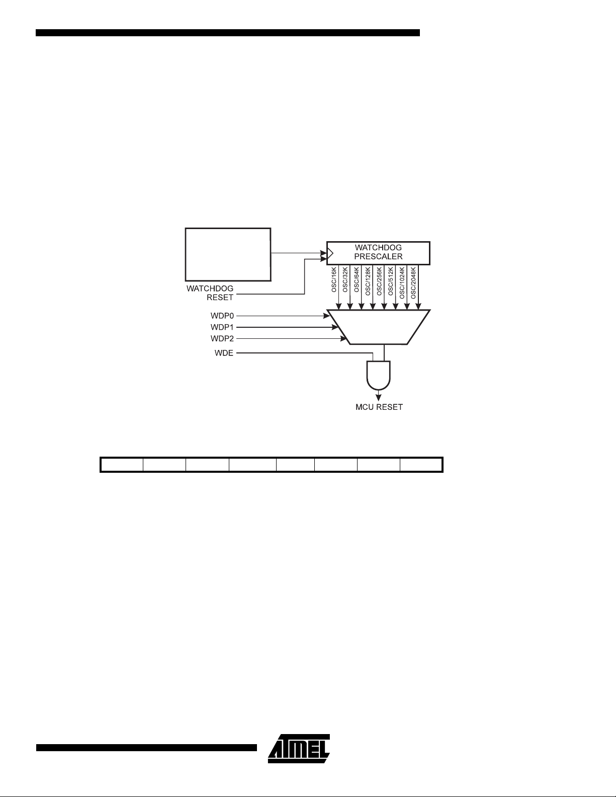
ATmega603/103
Watchdog Timer
The Watchdog Timer is clocked from a separate on-chip os cillator. By controlling the Watc hdog Timer prescaler, the
Watchdog reset interval can be adjusted as shown in Table 22. See characterization data for typical values at other V
levels. The WDR - Watchdog Reset - instruction resets the Watchdog Timer. From the Watchdog is reset, eight different
clock cycle periods can be sel ected to determine the res et period. If the reset period expires without another Watc hdog
reset, the ATmega603/103 resets and executes from the reset vector. For timing details on the Watchdog reset, refer to
page 28.
To prevent unintentional disabling of the watchdog, a special turn-off procedure must be followed when the watchdog is
disabled. Refer to the description of the Watchdog Timer Control Register for details.
Figure 36. Watchdog Timer
Oscillator
CC
1 MHz at V
350 kHz at V
CC
CC
= 5V
= 3V
Watchdog Timer Control Register - WDTCR
Bit 765 43210
$21 ($41) - - - WDTOE WDE WDP2 WDP1 WDP0 WDTCR
Read/Write R R R R/W R/W R/W R/W R/W
Initial value 0 0 0 0 0 0 0 0
Bits 7..5 - Res: Reserved bits
•
These bits are reserved bits in the ATmega603/103 and will always read as zero.
Bit 4 - WDTOE: Watch Dog Turn Off Enable
•
This bit must be set ( one ) whe n t he WDE b it is cleared, Otherwise, the watchdog will n ot be dis ab le d. On ce s et, hard w are
will clear this bit to zero after four clock cycles. Refer to the description of the WDE bit for a watchdog disable procedure.
Bit 3 - WDE: Watch Dog Enable
•
When the WDE is set (one) the Watchdog Timer is enabled, and if the WDE is cleared (zero) the Watchdog Timer function
is disabled. WDE can only be cleared if the WDTOE bit is set (one). To disable an enabled watchdog timer, the following
procedure must be followed:
1. In the same operation, write a logical one to WDTOE and WDE. A logical one must be written to WDE even though
it is set to one before the disable operation starts.
2. Within the next four clock cycles, write a logical 0 to WDE. This disables the watchdog.
Bits 2..0 - WDP2, WDP1, WDP0: Watch Dog Timer Prescaler 2, 1 and 0
•
The WDP2, WDP1 and WDP0 bits determine the Watchdog Timer prescaling when the Watchdog Timer is enabled. The
different prescaling values and their corresponding Time-out Periods are shown in Table 22.
51
Page 52

Table 22. Watch Dog Timer Prescale Select
Number of WDT Oscillator
WDP2 WDP1 WDP0
0 0 0 16K cycles 47 ms 15 ms
0 0 1 32K cycles 94 ms 30 ms
0 1 0 64K cycles 0.19 s 60 ms
0 1 1 128K cycles 0.38 s 0.12 s
1 0 0 256K cycles 0.75 s 0,24 s
1 0 1 512K cycles 1.5 s 0.49 s
1 1 0 1,024K cycles 3.0 s 0.97 s
1 1 1 2,048K cycles 6.0 s 1.9 s
Note: The frequency of the watchdog oscillator is voltage dependent as shown in the Electrical Characteristics section.
The WDR - Watchdog Reset - instruction should always be executed before the Watchdog Timer is enabled. This ensures that
the reset period will be in accordance with the Watchdog Timer prescale settings. If the Watchdog Timer is enabled without
reset, the watchdog timer may not start counting from zero.
cycles
Typical time-out
at Vcc = 3.0V
Typical time-out
at Vcc = 5.0V
EEPROM Read/Write Access
The EEPROM access registers are accessible in the I/O space.
The write access time is in th e r ang e of 2 .5 - 4ms , de pen di ng on the V
ware detect when the next byte can be written. A special EEPROM Ready interrupt can be set to trigger when the
EEPROM is ready to accept new data.
In order to prevent un intent ional E EPROM writes, a s pecific write pro cedur e must be followe d. Refer to the descrip tion of
the EEPROM control register for details on this.
When the EEPROM is written, the CPU is halted for two c lock cycles before th e next instruction is ex ecuted. When it is
read, the CPU is halted for 4 clock cycles.
voltages. A self- ti mi ng fu nc tio n le ts th e us er s oft-
CC
EEPROM Address Register - EEARH, EEARL
Bit 15141312 11 10 9 8
$1F ($3F) - - - - EEAR11 EEAR10 EEAR9 EEAR8 EEARH
$1E ($3E) EEAR7 EEAR6 EEAR5 EEAR4 EEAR3 EEAR2 EEAR1 EEAR0 EEARL
7654 3 2 10
Read/Write R R R R R/W R/W R/W R/W
R/W R/W R/W R/W R/W R/W R/W R/W
Initial value 0 0 0 0 0 0 0 0
0000 0 0 00
The EEPROM Address Re gis ters - EEARH and EEARL sp eci fy the E EP RO M add r ess in the 2K /4K - by te EE P ROM sp ac e.
The EEPROM data bytes are addressed linearly between 0 and 2047/4095. The ATmega603 has an EEPROM address
space of 2K, and the EEAR11 I/O bit is read-only with initial value of 0.
52
ATmega603/103
Page 53
ATmega603/103
EEPROM Data Register - EEDR
Bit 76543210
$1D ($3D) MSB LSB EEDR
Read/Write R/W R/W R/W R/W R/W R/W R/W R/W
Initial value00000000
•
Bits 7..0 - EEDR7..0: EEPROM Data:
For the EEPROM writ e o peration , the E EDR reg ister contai ns th e data to be writ ten to the E EPROM in the ad dress give n
by the EEAR register. For the EEPROM read operation, the EEDR contains the data read out from the EEPROM at the
address given by EEAR.
EEPROM Control Register - EECR
Bit 76543 210
$1C ($3C) - - - - EERIE EEMWE EEWE EERE EECR
Read/Write R R R R R R/W R/W R/W
Initial value 0 0 0 0 0 0 0 0
Bits 7..4 - Res: Reserved bits
•
These bits are reserved bits in the ATmega603/103 and will always be read as zero.
Bit 3 - EERIE: EEPROM Ready Interrupt Enable
•
When the I bit in SREG and EERIE are set (one), the EEPROM Ready Interrupt is enabled. When cleared (zero), the interrupt is disabled. The EEPROM Ready interrupt constantly generates an interrupt request when EEWE is cleared (zero).
Bit 2 - EEMWE: EEPROM Master Write Enable
•
The EEMWE bit determines whether setting EEWE to one causes the EEPROM to be written. When EEMWE is set(one)
setting EEWE will wri te d ata t o the EE PROM at the selected addr es s If E EM WE is zer o, s ett ing EE WE will hav e n o ef fec t.
When EEMWE has been set (one) by softwa re, hardwa re clears the bit to zero after four cloc k cycles. See the des criptio n
of the EEWE bit for a EEPROM write procedure.
Bit 1 - EEWE: EEPROM Write Enable
•
The EEPROM Write Enable Signal EEWE is the write strobe to the EEPROM. When address and data are correctly set up,
the EEWE bit must be set to write the value into the EEPROM. The EEMWE bit must be set when the logical one is written
to EEWE, otherwise no EEP ROM write takes p lace. The following proc edure should be follow ed when writing the
EEPROM (the order of steps 2 and 3 is unessential):
1. Wait until EEWE becomes zero.
2. Write new EEPROM address to EEAR (optional)
3. Write new EEPROM data to EEDR (optional)
4. Write a logical one to the EEMWE bit in EECR
5. Within four clock cycles after setting EEMWE, write a logical one to EEWE.
Caution: An interrupt between step 4 and step 5 will make the write cycle fail, since the EEPROM Master Write Enable will
time-out. If an interrupt routine accessing the EEPROM is interrupting another EEPROM access, the EEAR and EEDR register will be modified, causing the interrupted EEPROM access to fail. It is recommended to have the global interrupt flag
cleared during the 4 last steps to avoid these problems.
When the write access time (typically 2.5 ms at V
(zero) by hardware. The user software can poll this bit and wait for a zero before writing the next byte. When EEWE has
been set, the CPU is halted for two cycles before the next instruction is executed.
Bit 0 - EERE: EEPROM Read Enable
•
The EEPROM Read Enable Signal EERE is the read strobe to the EEPROM. When the correct address is s et up in the
EEAR register, the EERE bit must be set. When the EERE bit is cleared (zero) by hardware, requested data is found in the
EEDR register. The EEPROM read access takes one instruction there is no need to poll the EERE bit. When EERE has
been set, the CPU is halted for four cycles before the next instruction is executed.
= 5V or 4 ms at VCC = 2.7V) has elap sed, th e EEWE bit is cle ared
CC
53
Page 54

The user should poll t he EE WE bi t before sta rting th e read oper ation. If a write oper ation i s in pr ogre ss when new data or
address is written to the EEPROM I/O registers, the write operation will be interrupted, and the result is undefined.
Prevent EEPROM Corruption
During periods of low V
EEPROM to operate properly. These issues are the same as for board level systems using the EEPROM, and the same
design solutions should be applied.
An EEPROM data cor ruptio n can be cau sed b y two si tuation s when the vo ltage is too low. Fi rst, a reg ular write s equenc e
to the EEPROM req uires a minim um vo ltage to opera te corr ectly . Sec ondly, th e CPU it se lf can execute i nstru ctio ns inco rrectly, if the supply voltage for executing instructions is too low.
EEPROM data corruption can easily be avoided by following these design recommendations (one is sufficient):
1. Keep the AVR RESET active (low) during periods of insufficient power supply voltage. This is best done by an external low V
note AVR 180 for design considerations regarding power-on reset and low voltage detection.
2. Keep the AVR core in Power Down Sleep Mode during periods of low V
ing to decode and execute instructions, effectively protecting the EEPROM registers from unintentional writes.
3. Store constants in Flash memory if the ability to change memory contents from software is not required. Flash
memory can not be updated by the CPU, and will not be subject to corruption.
Reset Protection circuit, often referred to as a Brown-Out Detector (BOD). Please refer to application
CC
the EEPROM data c an be c orru pte d b ec ause the supply volta ge is to o l ow for the CPU and the
CC,
. This will prevent the CPU from attempt-
CC
Serial Peripheral Interface - SPI
The Serial Peripheral Interface (SPI) allows high-speed synchronous data transfer between the ATmega603/103 and
peripheral devices or between several AVR devices. The ATmega603/103 SPI features include the following:
• Full-Duplex, 3-Wire Synchronous Data Transfer
• Master or Slave Operation
• LSB First or MSB First Data Transfer
• Four Programmable Bit Rates
• End of Transmission Interrupt Flag
• Write Collision Flag Protection
• Wake-up from Idle Mode (Slave Mode Only)
54
ATmega603/103
Page 55

Figure 37. SPI Block Diagram
ATmega603/103
The interconnection between master and slave CPUs with SPI is shown in Figure 38. The PB1(SCK) pin is the clock output
in the master mode and is th e cl ock in put in the s lave mode . Writi ng to the S PI dat a regis ter of the master CPU s tarts th e
SPI clock generator, and the data written shifts out of the PB2(MOSI) pin and into the PB2 (MOSI) pin of the slave CPU.
After shifting one byte, the SPI clock generator stops, setting the end of transmission flag (SPIF). If the SPI interrupt enable
bit (SPIE) in the SPCR register is set, an interrupt is requested. The Slave Select input, PB0(SS
individual slave SPI device. The two shift registers in the Master and the Slave can be considered as one distributed 16-bit
circular shift register. This is shown in Figure 38. When data is shifted from the master to the slave, data is also shifted in
the opposite direction, simultaneously. This means that during one shift cycle, data in the master and the slave are
interchanged.
), is set low to select an
55
Page 56

Figure 38. SPI Master-Slave Interconnection
MSB LSB
8 BIT SHIFT REGISTER
SPI
CLOCK GENERATOR
MASTER
MISO
MISO
MOSI MOSI
SCK
SCK
SS SS
V
CC
MSB LSB
8 BIT SHIFT REGISTER
SLAVE
The system is single buffered in the transmit direction and double buffered in the receive direction. This means that characters to be transmitted cannot be written to the SPI Data Register before the entire shift cycle is completed. When receiving
data, however, a recei ve d b yte mu st be read from the SP I Data Register before the nex t b yte ha s bee n c om ple tel y sh ifte d
in. Otherwise, the first byte is lost.
When the SPI is enabled, the data direction of the MOSI, MISO, SCK and SS
pins is overridden ac cor d ing to th e fol lo wing
table:
Table 23. SPI Pin Overrides
PIN Direction, Master SPI Direction, Slave SPI
MOSI User Defined Input
MISO Input User Defined
SCK User Defined Input
SS
Note: See “Alternate Functions of Port B” on page 78 for a detailed description and how to define the direction of the user
defined SPI pins.
User Defined Input
SS Pin Functionality
When the SPI is configured as a master (MSTR in SPCR is set), the user can determine the direction of the SS
configured as an output, the pin i s a general output pin which does not affect the SPI s ystem. If SS
input, it must be hold high to ensure Master SPI operation. If the SS
configured as master with the SS
pin defined as an input, the SPI system interprets this as another master selecting the
pin is driven low by peripheral circuitry when the SPI is
is configured as an
pin. If SS is
SPI as a slave and starting to send data to it. To avoid bus contention, the SPI system takes the following actions:
1. The MSTR bit in SPCR is cleared and the SPI system becomes a slave. As a result of the SPI becoming a slave, the
MOSI and SCK pins become inputs.
2. The SPIF flag in SPSR is set, and if the SPI interrupt is enabled and the I-bit in SREG is set, the interrupt routine will
be executed.
Thus, when interrupt-driven SPI transmittal is used in master mode, and there exists a possibility that SS
is driven low, the
interrupt should a lwa ys c he ck that the MSTR bit is s til l se t. O n ce the MS TR b it has b een c lear ed by a sl av e s elec t, i t mus t
be set by the user to re-enable SPI master mode.
When the SPI is configured as a slave, the SS
becomes an output if configured so by the user. All other pins are inputs. When SS
the SPI is passive, whic h m eans tha t it wil l no t rece iv e i nc oming data. Note that the SPI logic will be reset once the SS
is brought high. If the SS
pin is brought high during a transmission, the SPI will stop sending and receiving immediately and
pin is always input. When SS is held low, the SPI is activated and MISO
is driven high, all pins are in puts, and
pin
both data received and data sent must be considered as lost.
56
ATmega603/103
Page 57

ATmega603/103
Data Modes
There are four combinations of SCK phase and polarity with respect to serial data, which are determined by control bits
CPHA and CPOL. The SPI data transfer formats are shown in Figure 39 and Figure 40.
Figure 39. SPI Transfer Format with CPHA = 0 and DORD = 0
SCK CYCLE #
(FOR REFERENCE)
SCK (CPOL=0)
SCK (CPOL=1)
1 2 3 4 5 6 7 8
(FROM MASTER)
MOSI
MISO
(FROM SLAVE)
SS (TO SLAVE)
SAMPLE
* Not defined but normally MSB of character just received
MSB 6 5 4 3 2 1 LSB
MSB
6 5 4 3 2 1 LSB
Figure 40. SPI Transfer Format with CPHA = 1and DORD = 0
SCK CYCLE #
(FOR REFERENCE)
SCK (CPOL=0)
SCK (CPOL=1)
MOSI
(FROM MASTER)
MISO
(FROM SLAVE)
SS (TO SLAVE)
SAMPLE
* Not defined but normally LSB of previously transmitted character.
1
MSB LSB
*
2
3
6
6
5
5
*
4
5
4
4
6
3
3
2
2
78
1
1
LSBMSB
SPI Control Register - SPCR
Bit 76543210
$0D ($2D) SPIE SPE DORD MSTR CPOL CPHA SPR1 SPR0 SPCR
Read/Write R/W R/W R/W R/W R/W R/W R/W R/W
Initial value00000000
Bit 7 - SPIE: SPI Interrupt Enable
•
This bit causes the SPI interrupt to be executed if SPIF bit in the SPSR register is set and the global interrupts are enabled.
Bit 6 - SPE: SPI Enable
•
When the SPE bit is set (one), the SPI is enabled and SS, MOSI, MISO and SCK are connected to pins PB0, PB1, PB2 and
PB3.
Bit 5 - DORD: Data Order
•
When the DORD bit is set (one), the LSB of the data word is transmitted first.
When the DORD bit is cleared (zero), the MSB of the data word is transmitted first.
57
Page 58

•
Bit 4 - MSTR: Master/Slave Select
This bit selects Master SPI mode when set (one), and Slave SPI mode when cleared (zero). If SS is configured as an input
and is driven low while MSTR is se t, MSTR will be cle ared, and SP IF in SPS R will be come set. The user will then have to
set MSTR to re-enable SPI master mode.
Bit 3 - CPOL: Clock Polarity
•
When this bit is s et (one) , SCK is hig h when idle. Wh en CPOL is c leared (zero), SCK i s low when i dle. Re fer to Fig ure 3 9
and Figure 40 for additional information.
Bit 2 - CPHA: Clock Phase
•
Refer to Figure 39 or Figure 40 for the functionality of this bit.
Bits 1,0 - SPR1, SPR0: SPI Clock Rate Select 1 and 0
•
These two bits control the SCK rate of the device configured as a master. SPR1 and SPR0 have no effect on the slave. The
relationship between SCK and the CPU Clock frequency f
Table 24. Rela tio ns hip Betwee n SCK and the Os c illat or Frequenc y
SPR1 SPR0 SCK Frequency
is shown in the following table:
cl
00
01
10
11
Note: Observe that CPU clock frequency can be lower than the XTAL frequency if the XTAL divider is enabled.
fcl / 4
fcl / 16
fcl / 64
fcl / 128
SPI Status Register - SPSR
Bit 76543210
$0E SPIF WCOL - - - - - - SPSR
Read/WriteRRRRRRRR
Initial value00000000
Bit 7 - SPIF: SPI Interrupt Flag
•
When a serial trans fer is complete, the SPIF bit is se t ( one) and an interrupt is ge nerat ed i f SP IE in S PC R is se t (o ne) an d
global interrupts are enabled. SPIF is cleared by hardware when executing the corresponding interrupt handling vector.
Alternatively, the SPIF bit is cl eared by first r eading the SPI s tatus register with S PIF set (one), the n accessing the SPI
Data Register (SPDR).
Bit 6 - WCOL: Write Collision flag
•
The WCOL bit is set if the SPI da ta registe r (SPDR) is written dur ing a dat a transfer . The WCOL bi t (and the SPIF bit) ar e
cleared (zero) by first reading the SPI Status Register with WCOL set (one), and then accessing the SPI Data Register.
Bit 5..0 - Res: Reserved bits
•
These bits are reserved bits in the ATmega603/103 and will always read as zero.
SPI Data Register - SPDR
Bit 76543210
$0F ($2F) MSB LSB SPDR
Read/Write R/W R/W R/W R/W R/W R/W R/W R/W
Initial value
XXXXXXXXUndefined
The SPI Data Register is a read/write register used for data transfer between the register file and the SPI Shift register.
Writing to the register initiates data transmission. Reading the register causes the Shift Register Receive buffer to be read.
58
ATmega603/103
Page 59

ATmega603/103
UART
The ATmega603/103 features a full duplex (separate receive and transmit registers) Universal Asynchronous Receiver and
Transmitter (UART). The main features are:
• Baud rate generator that can generate a large number of baud rates (bps)
• High baud rates at low XTAL frequencies
• 8 or 9 bits data
• Noise filtering
• Overrun detection
• Framing Error detection
• False Start Bit detection
• Three separate interrupts on TX Complete, TX Data Register Empty and RX Complete
Data Transmission
A block schematic of the UART transmitter is shown in Figure 41
Data transmission is initiated by writing the data to be transmitted to the UART I/O Data Register, UDR. Data is transferred
from UDR to the Transmit shift register when:
• A new character has been written to UDR after the stop bit from the previous character has been shifted out. The shift
register is loaded immediately.
• A new character has been written to UDR before the stop bit from the previous character has been shifted out. The shift
register is loaded when the stop bit of the character currently being transmitted has been shifted out.
If the 10(11)-bit Transmitter shift register is empty, data is transferred from UDR to the shift register. At this time the UDRE
(UART Data Register Empty) bit in the UART Status Register, USR, is set. When this bit is set (one), the UART is ready to
receive the next character. Writing to UDR clears UDRE. At the same time as the data is transferred from UDR to the
10(11)-bit shift register, bit 0 of the shift register is cleared (start bit) and bit 9 or 10 is set (stop bit). If 9 bit da ta word is
selected (the CHR9 bit in the UART Control Regi ster, UCR is set), t he TX B8 bit i n UCR is transferred to bit 9 in the Transmit shift register.
.
59
Page 60

Figure 41. UART Transmitter
DATA BUS
XTAL
CONTROL LOGIC
BAUD RATE
GENERATOR
BAUD x 16
STORE UDR
SHIFT ENABLE
IDLE
/16
BAUD
RXEN
TXEN
CHR9
RXB8
UART CONTROL
REGISTER (UCR)
RXCIE
TXCIE
UDRIE
DATA BUS
UART I/O DATA
REGISTER (UDR)
10(11)-BIT TX
SHIFT REGISTER
TXCTXC
TXB8
RXC
UART STATUS
REGISTER (USR)
TXC
IRQ
UDRE
FE
UDRE
PIN CONTROL
LOGIC
1
TXD
OR
UDRE
IRQ
On the Baud Rate clock follo wing the transf er opera tion to the shift r egister, the start bit is shifte d out on the TXD pin, fol lowed by the data, L SB first. When the sto p bit has b een shif ted out, th e shift r egister is loaded i f any new da ta has been
written to the UDR during the transmission. During loading, UDRE is set. If there is no new data in the UDR register to send
when the stop bit is shi fted out, the UDRE f lag wil l remai n set. In this case, a fter the stop b it has been pr esent on TX D for
one bit length, the TX Complete Flag, TXC, in USR is set.
The TXEN bit in UCR enables the UART transmitter when set (one). When this bit is cleared (zero), the PE1 pin can be
used for general I/O. When TXEN is set, the UART Transmitter will be connected to PE1, which is forced to be an output
pin regardless of the setting of the DDE1 bit in DDRE.
60
ATmega603/103
Page 61

Data Reception
Figure 42. UART Receiver
XTAL
RXD
BAUD RATE
GENERATOR
PIN CONTROL
LOGIC
DATA BUS
BAUD X 16 BAUD
DATA RECOVERY
/16
STORE UDR
LOGIC
ATmega603/103
UART I/O DATA
REGISTER (UDR)
10(11)-BIT RX
SHIFT REGISTER
RXB8
TXB8
TXEN
CHR9
RXEN
UART CONTROL
REGISTER (UCR)
UDRIE
DATA BUS
RXCIE
TXCIE
UDRE
RXC
TXC
FE
DOR
UART STATUS
REGISTER (USR)
RXC
RXC
IRQ
The receiver front-end logic samples the signal on the RXD pin at a frequency 16 times the baud rate. While the line is idle,
one single sample of logical zero will be interpreted as the falling edge of a start bit, and the start bit detection sequence is
initiated. Let sample 1 denote the first zero-sample. Following the 1 to 0-transition, the receiver samples the RXD pin at
sample 8, 9, and 10. If two or more of these thre e sampl es are found to be logical ones, the st art bit is reje cted as a no ise
spike and the receiver starts looking for the next 1 to 0-transition.
If however, a valid start bit is detected, sampling of the data bits following the start bit is performed. These bits are also
sampled at samples 8, 9, an d 10. The logic al val ue found in at least two of th e thre e sam ples is taken as the bit valu e. Al l
bits are shifted into the transmitter shift register as they are sampled. Sampling of an incoming character is shown in Figure
43.
Figure 43. Sampling Received Data
RXD
START BIT D0 D1 D2 D3 D4 D5 D6 D7 STOP BIT
RECEIVER
SAMPLING
61
Page 62

When the stop bit e nte rs the rece iver, t he maj orit y of the thr ee sam ple s mu st be one to acc ept th e stop bit. If two or m ore
samples are logical z er os , the Fram ing Error (FE) flag in the UAR T Statu s Re gi ste r (US R ) is set when th e r ec eived byte is
transferred to UDR. Before reading the UDR register, the user should always check the FE bit to detect Framing Errors. FE
is cleared when UDR is read.
Whether or not a valid stop bit is detected at the end of a character reception cycle, the data is transferred to UDR and the
RXC flag in USR is set. UDR is in fact two physically separate registers, one for transmitted data and one for received data.
When UDR is read, the Receive Data register is accessed, and when UDR is written, the Transmit Data register is
accessed. If 9 bit d ata word is select ed (the CHR9 bit in th e UART Contr ol Regist er, UCR is set ), the RXB 8 bit in UCR is
loaded with bit 9 in the Transmit shift register when data is transferred to UDR.
If, after having received a character, the UDR register has not been accessed since the last receive, the OverRun (OR) flag
in USR is set. This means that the new data transferred to the shift register could not be transferred to UDR and is lost. The
OR bit is buffered, and is available when the valid data byte in UDR ha s been read . The user sh ould al ways check the OR
after reading from the UDR register in order to detect any overruns if the baud rate is high or CPU load is high.
When the RXEN bit in the UCR register is cleared (zero), the receiver is disabled. This means that the PE0 pin can be used
as a general I/O pin. When RXEN is set, the UART Receiver will be connected to PE0, which is forced to be an input pin
regardless of the setting o f the DD E0 bi t in DDRE. W hen P E0 is f orced to i nput by th e UART, t he PO RTE0 bit c an stil l be
used to control the pull-up resistor on the pin.
When the CHR9 bit in the UCR register is set, transmitted and received characters are 9-bit long plus start and stop bits.
The 9th data bit to be transmitt ed is the TXB8 bi t in UCR reg ister. This b it must be set to th e wanted v alue befor e a transmission is initated by writing to the UDR register. The 9th
UART Control
UART I/O Data Register - UDR
Bit 76543210
$0C ($2C) MSB LSB UDR
Read/Write R/W R/W R/W R/W R/W R/W R/W R/W
Initial value00000000
The UDR register is actually two physi cally separate registers sharing the same I/O address. Wh en writi ng to the reg ister,
the UART Transmit Data register is written. When reading from UDR, the UART Receive Data register is read.
UART Status Register - USR
Bit 76543210
$0B ($2B) RXC TXC UDRE FE OR - - - USR
Read/Write R R/W R R R R R R
Initial value00100000
The USR register is a read-only register providing information on the UART Status.
Bit 7 - RXC: UART Receive Complete
•
This bit is set (one) when a received character is transferred from the Receiver Shift register to UDR. The bit is set regard-
less of any detected framing errors. When the RXCIE bit in UCR is set, the UART Receive Complete interrupt will be
executed when RXC is set(one). RXC is cleared by reading UDR. Wh en interrupt -driven da ta recept ion is used, the UART
Receive Complete Interrupt routine must read UDR in order to clear RXC, otherwise a new interrupt will occur once the
interrupt routine terminates.
Bit 6 - TXC: UART Transmit Complete
•
This bit is set (one) when the entire character (including the stop bit) in the Transmit Shift register has been shifted out and
no new data has been written to the UDR. This flag is especially useful in half-duplex communi cations interfaces, where a
transmitting application must enter r eceive mode and free th e communications bus immediately after compl eting the
transmission.
62
ATmega603/103
Page 63

ATmega603/103
When the TXCIE bit in UCR is set, setting of TXC causes the UART Transmit Complete interrupt to be executed. TXC is
cleared by hardware when executing the corresponding interrupt handling vector. Alternatively, the TXC bit is cleared
(zero) by writing a logical one to the bit.
•
Bit 5 - UDRE: UART Data Register Empty
This bit is set (one) when a character written to UDR is transferred to the Transmit shift register. Setting of this bit indicates
that the transmitter is ready to receive a new character for transmission.
When the UDRIE bit in UCR is set, the UART Transmit Complete interrupt to be executed as long as UDRE is set. UDRE is
cleared by writing UDR. When interrupt-driven data transmittal is used, the UART Data Register Empty Interrupt routine
must write UDR in order to clear UDRE, otherwise a new interrupt will occur once the interrupt routine terminates.
UDRE is set (one) during reset to indicate that the transmitter is ready.
Bit 4 - FE: Framing Error
•
This bit is set if a Framing Error condition is detected, i.e. when the stop bit of an incoming character is zero.
The FE bit is cleared when the stop bit of received data is one.
Bit 3 - OR: OverRun
•
This bit is set if an Overr un condit ion is d etected, i. e. when a character already pres ent in th e UDR registe r is n ot read
before the next character is transferred from the Receive r Shift register . The OR bit is buffer ed, which means tha t it is will
be set once the valid data still in UDRE is read.
The OR bit is cleared (zero) when data is received and transferred to UDR.
Bits 2..0 - Res: Reserved bits
•
These bits are reserved bits in the ATmega603/103 and will always read as zero.
UART Control Register - UCR
Bit 76543210
$0A ($2A) RXCIE TXCIE UDRIE RXEN TXEN CHR9 RXB8 TXB8 UCR
Read/Write R/W R/W R/W R/W R/W R/W R W
Initial value00000010
Bit 7 - RXCIE: RX Complete Interrupt Enable
•
When this bit is set (one), a setting of the RXC bit in USR will cause the Receive Complete interrupt routine to be executed
provided that global interrupts are enabled.
Bit 6 - TXCIE: TX Complete Interrupt Enable
•
When this bit is set (one), a setting of the TXC bit in USR will cause the Transmit Complete interrupt routine to be executed
provided that global interrupts are enabled.
Bit 5 - UDRIE: UART Data Register Empty Interrupt Enable
•
When this bit is set (one), a setting of the UDRE bit in USR will cause the UART Data Register Empty interrupt routine to be
executed provided that global interrupts are enabled.
Bit 4 - RXEN: Receiver Enable
•
This bit enables the UART receiver when set (one). When the receiver is disabled, the TXC, OR and FE status flags cannot
become set. If these flags are set, turning off RXEN does not cause them to be cleared.
Bit 3 - TXEN: Transmitter Enable
•
This bit enables the UART transmitter when set (one). When disabling the transmitter while transmitting a character, the
transmitter is not disabled before the character in the shift regi ster plus any fol lowing character in UDR has been completely transmitted.
Bit 2 - CHR9: 9 Bit Characters
•
When this bit is set (one) transmitted and received characters are 9 bit long plus start and stop bits. The 9th bit is read and
written by using the RXB8 and TXB8 bits in UCR, respectively. The 9th data bit can be used as an extra stop bit or a parity
bit.
Bit 1 - RXB8: Receive Data Bit 8
•
When CHR9 is set (one), RXB8 is the 9th data bit of the received character.
63
Page 64

•
Bit 0 - TXB8: Transmit Data Bit 8
When CHR9 is set (one), TXB8 is the 9th data bit in the character to be transmitted.
Baud Rate Generator
The baud rate generator is a frequency divider which generates baud rates according to the following equation:
f
BAUD
CK
------------------------------------- -=
16 UBRR 1+
()
• BAUD = Baud Rate
= CPU Clock frequency
•f
CK
• UBRR = Contents of the UART Baud Rate register, UBRR (0 - 255)
For standard crystal frequencies, the most commonly used baud rates c an be generated by using the UBRR settings in
Table 25. Observe that CPU c lock fr equency can be l ower than th e XTAL frequency if the XTAL divider is enabled. UBRR
values which yiel d an actua l baud rate di ffering l ess than 2% from the tar get baud r ate, are bol ded in the table. Howe ver,
using baud rates that have more than 1% error is not recommended. High error ratings give less noise resistance.
Table 25. UBRR Settings at Various CPU Frequencies
Baud Rate
2400
4800
9600
14400
19200
28800
38400
57600
76800
115200
Baud Rate
2400
4800
9600
14400
19200
28800
38400
57600
76800
115200
1MHz
UBRR=
UBRR=
UBRR= 6 7 .5 UB RR=
UBRR= 3 7 .8 UB RR=
UBRR= 2 7 .8 UB RR=
UBRR= 1 7 .8 UB RR=
UBRR= 1 22.9 UB RR=
UBRR= 0 7 .8 UB RR=
UBRR= 0 22.9 UB RR= 1 33.3 UBRR= 1 22.9 UB RR=
UBRR= 0 84.3 UB RR=
3.2768 MHz
UBRR=
UBRR=
UBRR=
UBRR=
UBRR= 1 0 3.1 UB RR=
UBRR=
UBRR= 4 6 .3 UB RR=
UBRR= 3 12.5 UB RR=
UBRR= 2 12.5 UB RR=
UBRR= 1 12.5 UB RR=
%Error
25 0.2
12 0.2
%Error
84 0.4
42 0.8
20 1.6
13 1.6
61.6
1.8432 MHz
UBRR=
UBRR=
3.6864 MHz
UBRR=
UBRR=
UBRR=
UBRR=
UBRR=
%Error
47 0.0
23 0.0
11 0.0
70.0
50.0
30.0
20.0
10.0
00.0
%Error
95 0.0
47 0.0
23 0.0
15 0.0
11 0.0
70.0
50.0
30.0
20.0
10.0
2MHz
UBRR=
UBRR=
UBRR=
UBRR= 8 3 .7 UB RR= 10 3.1
UBRR= 6 7 .5 UB RR=
UBRR= 3 7 .8 UB RR= 4 6.3
UBRR= 2 7 .8 UB RR=
UBRR= 1 7 .8 UB RR= 2 12.5
UBRR= 0 7 .8 UB RR= 0 25.0
4MHz
UBRR=
UBRR=
UBRR=
UBRR= 1 6 2.1 UB RR=
UBRR=
UBRR= 8 3 .7 UB RR=
UBRR= 6 7 .5 UB RR= 7 6.7
UBRR= 3 7 .8 UB RR=
UBRR= 2 7 .8 UB RR= 3 6.7
UBRR= 1 7 .8 UB RR= 2 20.0
%Error
51 0.2
25 0.2
12 0.2
%Error
103 0.2
51 0.2
25 0.2
12 0.2
2.4576 MHz
UBRR=
UBRR=
UBRR=
4.608 MHz
UBRR=
UBRR=
UBRR=
UBRR=
%Error
63 0.0
31 0.0
15 0.0
70.0
30.0
10.0
%Error
119 0.0
59 0.0
29 0.0
19 0.0
14 0.0
90.0
40.0
64
Baud Rate
2400
4800
9600
14400
19200
28800
38400
57600
76800
115200
7.3728 MHz
UBRR=
UBRR=
UBRR=
UBRR=
UBRR=
UBRR=
UBRR=
UBRR=
UBRR=
UBRR=
%Error
191 0.0
95 0.0
47 0.0
31 0.0
23 0.0
15 0.0
11 0.0
70.0
50.0
30.0
ATmega603/103
8MHz
UBRR=
UBRR=
UBRR=
UBRR=
UBRR=
UBRR= 1 6 2.1 UB RR=
UBRR=
UBRR= 8 3 .7 UB RR=
UBRR= 6 7 .5 UB RR= 7 6.7 UB RR=
UBRR= 3 7 .8 UB RR=
%Error
207 0.2
103 0.2
51 0.2
34 0.8
25 0.2
12 0.2
9.216 MHz
UBRR=
UBRR=
UBRR=
UBRR=
UBRR=
UBRR=
%Error
239 0.0
119 0.0
59 0.0
39 0.0
29 0.0
19 0.0
14 0.0
90.0
40.0
11.059 MHz
UBRR= 287 UBRR=
UBRR=
UBRR=
UBRR=
UBRR=
UBRR=
UBRR=
UBRR=
%Error
143 0.0
71 0.0
47 0.0
35 0.0
23 0.0
17 0.0
11 0.0
80.0
50.0
Page 65
ATmega603/103
UART Baud Rate Register - UBRR
Bit 76543210
$09 ($29) MSB LSB UBRR
Read/Write R/W R/W R/W R/W R/W R/W R/W R/W
Initial value00000000
The UBRR is an 8-bit read/write register which specifies the UART Baud Rate according to the description on the previous
page.
Analog Comparator
The analog comparator compares the input values on the positive input PE2 (AC+) and negative input PE3 (AC-). When
the voltage on the positive input PE2 (AC+) is higher than the voltage on the negative input PE3 (AC-), the Analog Comparator Output, ACO is set (one) . The output of the compara tor can be set to trigger the Timer /Counter1 Input Captur e
function. In addition, the comparator can trigger a separate interrupt, exclusive to the Analog Comparator. The user can
select Interrupt trigg ering on compar ator o utput ris e, fall, or toggle . A blo ck diagram of th e compar ator and it s sur roundin g
logic is shown in Figure 44.
Figure 44. Analog Comparator Block Diagram
VCC
ACD
PE2
(AC+)
PE3
(AC-)
+
-
INTERRUPT
SELECT
ACIS1 ACIS0
ACIE
ACIC
ACO
ANALOG
COMPARATOR
IRQ
ACI
TO T/C1 CAPTURE
TRIGGER MUX
Analog Comparator Control and Status Register - ACSR
Bit 76543210
$08 ($28) ACD - ACO ACI ACIE ACIC ACIS1 ACIS0 ACSR
Read/Write R/W R R R/W R/W R/W R/W R/W
Initial value00000000
Bit 7 - ACD: Analog Comparator Disable
•
When this bit is set( one ), th e p ower to the analog comparato r is sw it ched off. This bit can be s et at any t ime to tu rn off the
analog comparato r. Thi s will red uce pow er c onsu mptio n in active and idle mode . Whe n ch ang ing t he AC D bit, the A nalo g
Comparator Interrupt mus t be disa bled by cl earing th e ACIE bi t in ACS R. Other wise an interr upt can o ccur when the bi t is
changed.
Bit 6 - Res: Reserved bit
•
This bit is a reserved bit in the ATmega603/103 and will always read as zero.
Bit 5 - ACO: Analog Comparator Output
•
ACO is directly connected to the comparator output.
65
Page 66

•
Bit 4 - ACI: Analog Comparator Interrupt Flag
This bit is set (one) when a comparator output event triggers the interrupt mode defined by ACI1 and ACI0. The Analog
Comparator Interrupt routine is executed if the ACIE bit is set (one) and the I-bit in SREG is set (one). ACI is cleared by
hardware when executing the corresponding interrupt handling vector. Alternatively, ACI is cleared by writing a logic one to
the flag. Observe however, that if another bit in this register is modified using the SBI or CBI instruction, ACI will be cleared
if it has become set before the operation.
Bit 3 - ACIE: Analog Comparator Interrupt Enable
•
When the ACIE bit is set (one) and the I-bit in the Status Register is set (one), the analog comparator interrupt is activated.
When cleared (zero), the interrupt is disabled.
Bit 2 - ACIC: Analog Comparator Input Capture enable
•
When set (one), this bit enables the Input Capture function in Timer/Counter1 to be triggered by the analog comparator.
The comparator output is in this case directly connected to the Input Capture front-end logic, making the comparator utilize
the noise canceler and edge select features of the Timer/Counter1 Input Capture interrupt. When cleared (zero), no connection between the analog comparator and the Input Capture function is giv en. To make the comparator trigger the
Timer/Counter1 Input Capture interrupt, the TICIE1 bit in the Timer Interrupt Mask Register (TIMSK) must be set (one).
Bits 1,0 - ACIS1, ACIS0: Analog Comparator Interrupt Mode Select
•
These bits determine which comparator events that trigger the Analog Comparator interrupt. The different settings are
shown in Table 26.
Table 26. ACIS1/ACIS0 Settings
ACIS1 ACIS0 Interrupt Mode
0 0 Comparator Interrupt on Output Toggle
01Reserved
1 0 Comparator Interrupt on Falling Output Edge
1 1 Comparator Interrupt on Rising Output Edge
When changing the ACIS1/ ACIS0 bits, The Anal og Com parator Interrup t must be dis abled by clea ring its Interr upt En able
bit in the ACSR register. Otherwise an interrupt can occur when the bits are changed.
Caution: Using the SBI or CBI instruction on other bits than ACI in this register, will write a one back into ACI if it is read as
set, thus clearing the flag.
Analog to Digital Converter
Feature list:
• 10-bit Resolution
• ±2 LSB absolute accuracy
• 0.5 LSB Integral Non-Linearity
• 70 - 280 µs conversi on time
• Up to 14 kSPS
• 8 Multiplexed Input Channels
• Interrupt on ADC conversion complete.
• Sleep Mode Noise Canceler
The ATmega603/103 features a 10-bit successive approximation ADC. The ADC is connected to an 8-channel Analog Mul-
tiplexer which allows each pin of Port F to be used as an input for the ADC. The ADC contains a Sample and Hold Amplifier
which ensures that the input voltag e to the ADC is held at a constant lev el dur ing conversion. A bloc k di agram of the ADC
is shown in Figure 45.
The ADC has two separate analog supply voltage pins, AV
age on AV
must not differ more t han ± 0.3 V from VCC. See the section “ADC Noise C ancel ing Tec hnique s” o n page 71
CC
on how to connect these pins.
and AGND. AGND must be connect ed to GND, and the volt-
CC
66
ATmega603/103
Page 67

ATmega603/103
An external reference voltage must be applied to the AREF pin. This voltage must be in the range AGND - AV
Figure 45. Analog to Digital Converter Block Schematic
ADC CONVERSION
COMPLETE IRQ
External
Reference
Voltage
Analog
Inputs
8-BIT DATA BUS
8-
CHANNEL
MUX
ADC MULTIPLEXER
SELECT (ADMUX)
-
+
SAMPLE & HOLD
COMPARATOR
MUX2
MUX1
ADC CTRL & STATUS
MUX0
ADIE
ADIF
REGISTER (ADCSR)
ADIF
ADIE
ADSC
ADEN
ADPS1
ADPS2
CONVERSION LOGIC10-BIT DAC
90
ADC DATA REGISTER
(ADCH/ADCL)
ADPS0
CC
.
Operation
The ADC operates in Single Conversion mode, and each conversion will have to be initiated by the user.
The ADC is enabled by writing a logical one to the ADC Enable bit, ADEN in ADCSR. The first conversion that is started
after enabling the A DC, wi ll be prec ed ed by a d umm y co nv er sion to initialize the A DC. To the user, the only diffe renc e w il l
be that this conversion takes 13 more ADC clock pulses than a normal conversion. (See Figure 48.)
A conversion is started by writing a logical one to the ADC Start Conversion bit, ADSC. This bit will stay high as long as the
conversion is in pr ogre ss an d be set to z ero b y ha rdwa re whe n the con vers ion is co mplet ed. I f a d iffer ent data chan nel is
selected while a co nversion is in progress, th e ADC will f inish the cur rent conversion be fore performi ng the channe l
change.
As the ADC generates a 10-bit result, two data registers, ADCH and ADCL, must be read to get the result when the conversion is complete . S pec ial data protection log ic i s us ed to en su re th at t he co nten ts of the data registers bel ong to th e s am e
result when they are read. This mechanism works as follows:
When reading data, ADCL must be read first. Once ADCL is read, ADC access to data registers is blocked. This means
that if ADCL has been read, an d a conv ersion c omple tes before ADCH is read, none of the regis ters are updated and the
result from the conversion is lost. When ADCH is read, ADC access to the ADCH and ADCL registers is re-enabled.
The ADC has its own interrupt, ADIF, which can be triggered when a conversion completes. When ADC access to the data
registers is prohibited between reading of ADCL and ADCH, the interrupt will trigger even if the result is lost.
67
Page 68
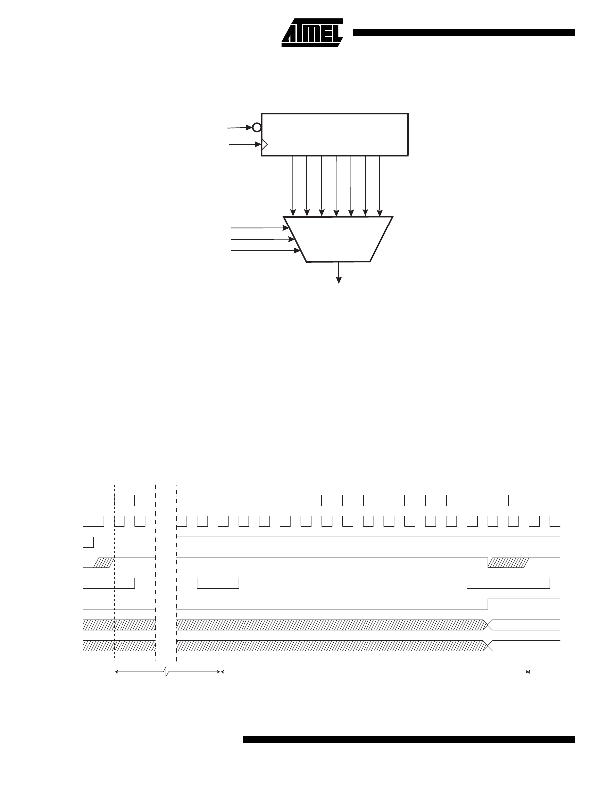
Prescaling
Figure 46. ADC Prescaler
ADEN
CK
ADPS0
ADPS1
ADPS2
Reset
7-BIT ADC PRESCALER
CK/2
CK/4
ADC CLOCK SOURCE
CK/8
CK/32
CK/16
CK/64
CK/128
The ADC contains a prescaler, which divides the system clock to an acceptable ADC clock frequency. The ADC accepts
input clock frequencies in the range 50 - 200 kHz. Applying a higher input frequency will result in a poorer accuracy, see
“ADC DC Characteristics” on page 72.
The ADPS0 - ADPS2 bits in A DCSR are used to g enerate a pr oper ADC cl ock input fre quency from any XTAL fre quency
above 100 kHz. The prescaler starts counting from the moment the ADC is switched on by setting the ADEN bit in ADCSR.
The prescaler keeps running for as long as the ADEN bit is set, and is continuously reset when ADEN is low.
When initiating a conversion by setting the ADSC bit in ADCSR, the conversion starts at the following falling edge of the
ADC clock cycle. The actual sample-and-hold takes place one ADC clock cycle after the start of the conversion. The result
is ready and written to the ADC Result Register after 13 cycles. The ADC needs 2 more clock cycles before a new conversion can be started. If ADSC is set high in this period, the ADC will start the new conversion immediately. For a summary of
conversion times, see Table 27.
Figure 47. ADC timing diagram, first conversion
Cycle number
ADC clock
ADEN
ADSC
Hold strobe
ADIF
ADCH
ADCL
68
1 21213 14 15 16 17 18 19 20 21 22 23 24 25 26 27 28 1 2
Dummy Conversion Actual Conversion
ATmega603/103
MSB of result
LSB of result
Second
Conversion
Page 69
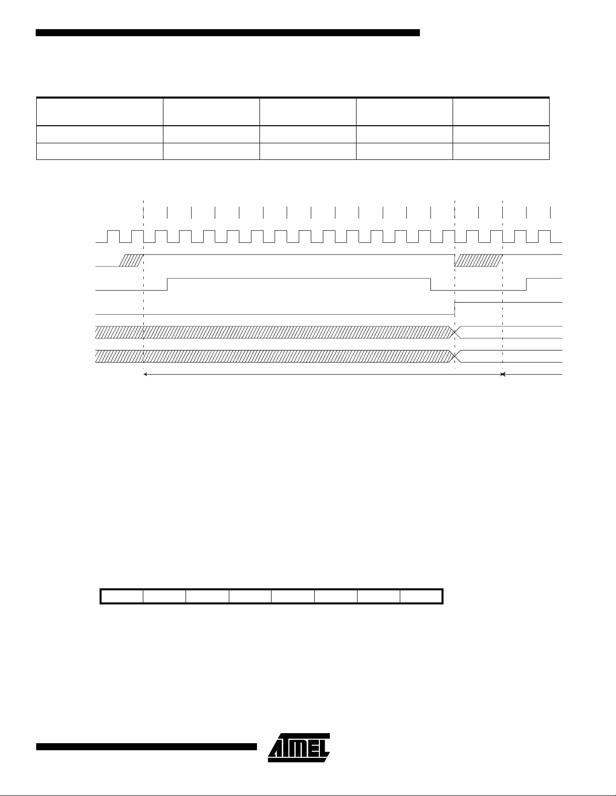
Table 27. ADC Conversion Time
ATmega603/103
Condition Sample Cycle
Number
1st Conversion 14 26 28 140 - 560
Single Conversion 1 13 15 75 - 300
Result Ready
(cycle number)
Total Conversion
Time (cycles)
Total Conversion
Time (µs)
Figure 48. ADC Timing Diagram
Cycle number
ADC clock
ADSC
Hold strobe
ADIF
ADCH
ADCL
1 2 3 4 5 6 7 8 9 10 11 12 13
One Conversion Next Conversion
14 15 12
MSB of result
LSB of result
ADC Noise Canceler Function
The ADC features a nois e canc el er th at e nabl es c onv ers ion du ring idl e m ode to r ed uc e no ise i ndu ce d fr om the CP U co r e.
To make use of this feature, the following procedure should be used:
1. Turn off the ADC by clearing ADEN.
2. Turn on the ADC and simultaneously start a conversion by setting ADEN and ADSC. This starts a dummy
conversion that will be followed by a valid conversion.
3. Within 14 ADC clock cycles, enter idle mo de.
4. If no other interrupts occur before the ADC conversion completes, the ADC interrupt will wake up the MCU and
execute the ADC conversion complete interrupt routine.
ADC Multiplexer Select Register - ADMUX
Bit 76543210
$07 ($27) - - - - - MUX2 MUX1 MUX0 ADMUX
Read/Write R R R R R R/W R/W R/W
Initial value00000000
Bits 7..3 - Res: Reserved Bits
•
These bits are reserved bits in the ATmega603/103 and always read as zero.
Bits 2..0 - MUX2..MUX0: Analog Channel Select Bits 2-0
•
The value of these three bits selects which analog input 7-0 is connected to the ADC.
69
Page 70

ADC Control and Status Register - ADCSR
Bit 76543210
$06 ($26) ADEN ADSC - ADIF ADIE ADPS2 ADPS1 ADPS0 ADCSR
Read/Write R/W R/W R R/W R/W R/W R/W R/W
Initial value00000000
•
Bit 7 - ADEN: ADC Enable
Writing a logical ‘1’ to this bit enables the ADC. By clearing this bit to zero, the ADC is turned off. Turning the ADC off while
a conversion is in progress, will terminate this conversion.
Bit 6 - ADSC: ADC Start Conversion
•
A logical ‘1’ must be written to this bit to start each conversion. The first time ADSC has been written after the ADC has
been enabled, or if ADSC is written at the same time as the ADC is enabled, a dummy conversion will precede the initiated
conversion. This dummy conversion performs initialization of the ADC.
ADSC remains high during the conversion. ADSC goes low after the conversion is complete, but before the result is written
to the ADC Da ta Regi st ers. This allo ws a ne w conv er sion to be i nitia te d be for e th e cur ren t co nver sion is compl ete . Th e ne w
conversion will the n star t imme diatel y after the cu rren t conv ersion c omple tes. W hen a dum my co nver sion p recedes a rea l
conversion, ADSC will stay high until the real conversion completes.
Writing a zero to this bit has no effect.
Bit 5 - Res: Reserved Bit
•
This bit is reserved in the ATmega603/103. Warning: When writing ADCSR, a logical “0” must be written to this bit.
Bit 4 -ADIF: ADC Interrupt Flag
•
This bit is set (one) when an ADC conversion is complete and the the result is written to the ADC Data Registers are
updated. The ADC Conversion Complete Interr upt is execute d if the ADIE bit and the I-bit in SREG are se t (one). ADIF is
cleared by hardware when executing the corresponding interrupt handling vector. Alternatively, ADIF is cleared by writing a
logical one to the flag. Bew are that if doing a read-mo dify- write on ADCSR, a pendin g inter rupt ca n be dis abled . This als o
applies if the SBI and CBI instructions are used.
Bit 3 - ADIE: ADC Interrupt Enable
•
When this bit is set (one) and the I-bit in SREG is set (one), the ADC Conversion Complete Interrupt is activated.
Bits 2..0 - ADPS2..ADPS0: ADC Prescaler Select Bits
•
These bits determine the division factor between the XTAL frequency and the input clock to the ADC.
Table 28. ADC Prescaler Selections
ADPS2 ADPS1 ADPS0 Division Factor
000 Invalid
001 2
010 4
011 8
100 16
101 32
110 64
111 128
70
ATmega603/103
Page 71
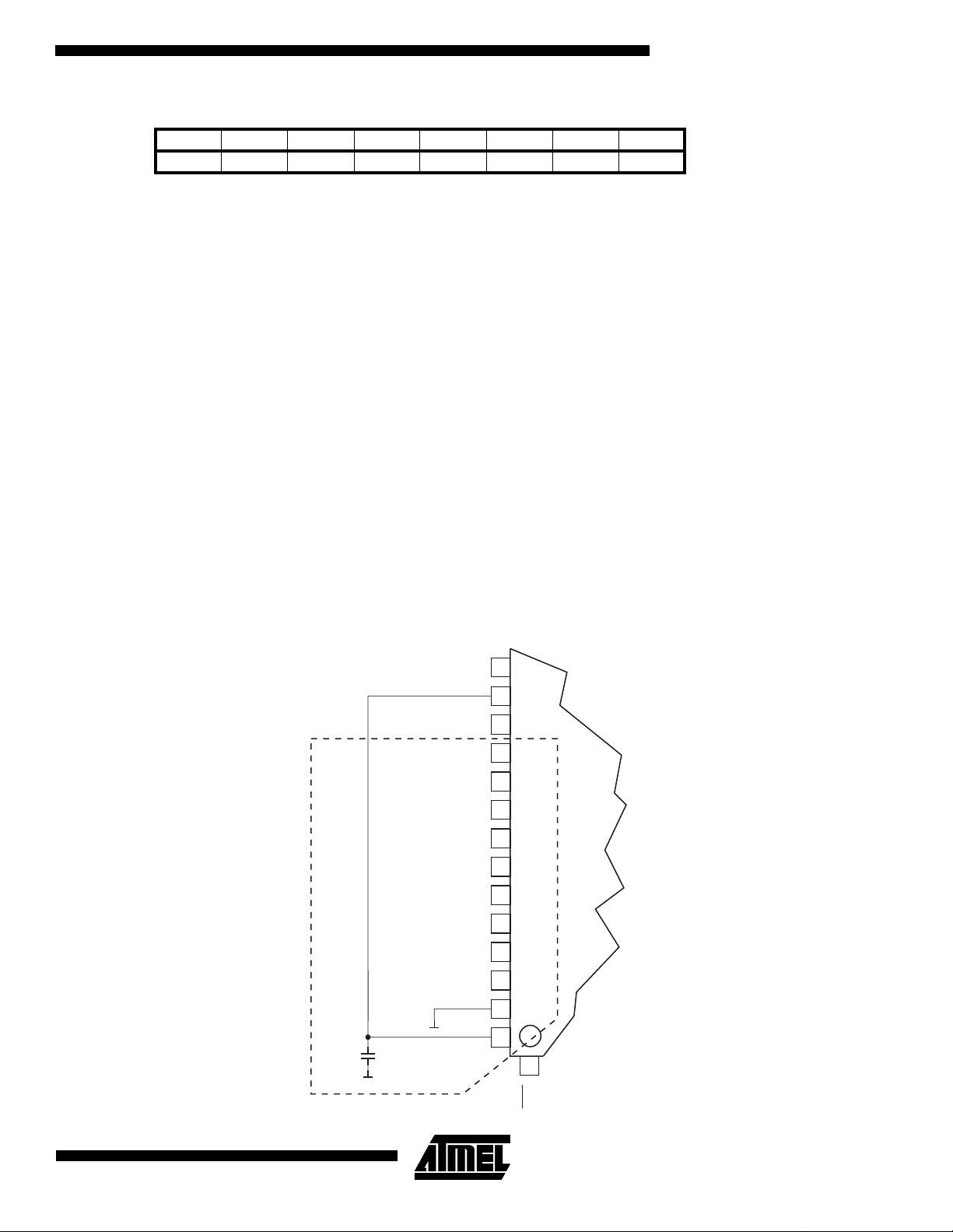
ATmega603/103
ADC Data Register - ADCL and ADCH
Bit 151413121110 9 8
$05 ($25) - - - - - - ADC9 ADC8 ADCH
$04 ($24) ADC7 ADC6 ADC5 ADC4 ADC3 ADC2 ADC1 ADC0 ADCL
76543210
Read/WriteRRRRRRRR
RRRRRRRR
Initial value00000000
00000000
When an ADC conversion is complete, the result is found in these two registers. It is essential that both registers are read,
and that ADCL is read before ADCH.
ADC Noise Canceling Techniques
Digital circuitry inside and outside the ATmega603/103 generates EMI which might affect the accuracy of analog measurements. If conversion accuracy is critical, the noise level can be reduced by applying the following techniques:
1. The analog part of the ATmega603/103 and all analog components in the application should have a separate analog ground plane on the PCB. This ground plane is connected to the digital ground plane via a single point on the
PCB.
2. Keep analog signal paths as short as possible. Make sure analog tracks run over the analog ground plane, and keep
them well away from high-speed switching digital tracks.
3. The AV
4. Use the ADC noise canceler function to reduce induced noise from the CPU.
5. If some Port F pins are used as digital inputs, it is essential that these do not switch while a conversion is in
progress.
pin on the ATmega603/103 should have its own decoupling capacitor as shown in Figure 49.
CC
Figure 49. ADC Power Connections
10nF
Analog Ground Plane
(AD0) PA0
VCC
GND
(ADC7) PF7
(ADC6) PF6
(ADC5) PF5
(ADC4) PF4
(ADC3) PF3
(ADC2) PF2
(ADC1) PF1
(ADC0) PF0
AREF
AGND
AVCC
51
52
53
54
55
56
57
58
59
ATmega603/103
60
6161
6262
6363
6464
1
PEN
71
Page 72

ADC DC Characteristics
TA=-40°C to 85°C
Symbol Parameter Condition Min Typ Max Units
Resolution 10 Bits
Absolute accuracy
VREF = 4V, V
ADC clock = 200 kHz
CC
= 4V
12LSB
Absolute accuracy
Absolute accuracy
Integral Non-Linearity VREF > 2V 0.5 LSB
Differential Non-Linearity VREF > 2V 0.5 LSB
Zero Error (Offset) 1 LSB
Conversion Time 70 280
Clock Frequency 50 200 kHz
AV
CC
V
REF
R
REF
R
AIN
Notes: 1. Minimum for AVCC is 2.7V.
Analog Supply Voltage VCC–0.3
Reference Voltage AGND AV
Reference Input Resistance 6 10 13 kΩ
Analog Input Resistan ce 100 MΩ
2. Maximum for AV
is 6.0V.
CC
VREF = 4V, V
ADC clock = 1 MHz
VREF = 4V, V
ADC clock = 2 MHz
CC
CC
= 4V
= 4V
4LSB
16 LSB
µs
(1)
VCC+0.3
CC
(2)
V
V
Interface to external SRAM
The interface to the SRAM consists of:
• Port A: Multiplexed low-order address bus and data bus
• Port C: High-order address bus
• The ALE-pin: Address latch enable
• The RD
The external data SRAM is ena bl ed b y sett ing the SRE - Externa l S RA M enabl e bi t of the MCUCR - M CU cont rol reg ister,
and will override th e setting of th e data directi on register DDR A. When the SR E bit is clear ed (zero), th e external dat a
SRAM is disabled, and the normal pin and data direction settings are used. When SRE is cleared (zero), the address space
above the internal SRAM boundary is not mapped into the internal SRAM, as in AVR parts not having interface to the
external SRAM.
When ALE goes from high to low, there is a valid address on Port A. ALE is low during a data transfer. RD
active when accessing the external SRAM only.
When the external SRAM is enabled, the ALE signal may have short pulses when accessing the internal RAM, but the ALE
signal is stable when accessing the external SRAM.
Figure 50 sketches how to connect an external SRAM to the AVR using 8 latches which are transparent when G is high.
Default, the external SRAM access is a three-cycle scheme as depicted in Figure 51. When one extra wait state is needed
in the access cycl e, se t the S RW bit (one ) in the MCU CR reg ister. Th e resul ting ac cess sche me is shown in Figur e 52. In
both cases, note that Port A is data bus in one cycle only. As soon as the data access finishes, Port A becomes a low order
address bus again.
and WR-pin: Read and write strobes.
and WR are
72
ATmega603/103
Page 73

ATmega603/103
For details in the timing for the SRAM interface, please refer to Figure 78, Table 46, Table 47, Table 48, and Table 49 in
section “DC Characteris tic s ” on page 105.
Figure 50. External SRAM connected to the AVR
D[7:0]
Port A
ALE
AVR
Port C
RD
WR
DQ
G
Figure 51. External SRAM Access Cycle without wait states
T1 T2 T3
System Clock Ø
ALE
Address [15..8]
Prev. Address
A[7:0]
SRAM
A[15:8]
RD
WR
Address
Data / Address [7..0]
WR
Data / Address [7..0]
RD
Prev. Address
Prev. Address
Address
Address
Data
Data
Address
WriteRead
Address
73
Page 74

Figure 52. External SRAM Access Cycle with wait state
T1 T2 T3 T4
System Clock Ø
ALE
Address [15..8]
Data / Address [7..0]
Prev. Address
Prev. Address
Address
Address
Data
Addr.
WriteRead
WR
Data / Address [7..0]
Prev. Address
Address
Data
Addr.
RD
I/O-Ports
All AVR ports h ave true Read-Modify-Write fun ctionality when used as ge ner al digital I/O ports. Thi s mea ns th at the direction of one port pin can be changed without unintentionally changing the direction of any other pin with the SBI and CBI
instructions. The same applies for changing drive value (if configured as output) or enabling/disabling of pull-up resistors (if
configured as input).
Port A
Port A is an 8-bit bi-directional I/O port with internal pull-ups.
Three I/O memory address locations are allocated for Port A, one each for the Data Register - PORTA, $1B($3B), Data
Direction Register - DDRA, $1A($3A) and the Port A Input Pins - PINA, $19($39). The Port A Input Pins address is read
only, while the Data Register and the Data Direction Register are read/write.
All port pins have indiv idually selecta ble pull-up resistors. T he Port A output buffers can sink 20mA and thu s drive LED
displays directly. When pins PA0 to PA7 are used as i nputs and are externally pulled low, they will sourc e current if the
internal pull-up resistors are activated.
The Port A pins have alternate functions related to the optional external data SRAM. Port A can be configured to be the
multiplexed low-order address/data bus during accesses to the byte.
When Port A is set to the alternate function by the SRE - External SRAM Enable - bit in the MCUCR - MCU Control Register, the alternate settings override the data direction register.
74
ATmega603/103
Page 75

ATmega603/103
Port A Data Register - PORTA
Bit 76543210
$1B ($3B) PORTA7 PORTA6 PORTA5 PORTA4 PORTA3 PORTA2 PORTA1 PORTA0 PORTA
Read/Write R/W R/W R/W R/W R/W R/W R/W R/W
Initial value00000000
Port A Data Direction Register - DDRA
Bit 76543210
$1A ($3A) DDA7 DDA6 DDA5 DDA4 DDA3 DDA2 DDA1 DDA0 DDRA
Read/Write R/W R/W R/W R/W R/W R/W R/W R/W
Initial value00000000
Port A Input Pins Address - PINA
Bit 76543210
$19 ($39) PINA7 PINA6 PINA5 PINA4 PINA3 PINA2 PINA1 PINA0 PINA
Read/WriteRRRRRRRR
Initial value Hi-Z Hi-Z Hi-Z Hi-Z Hi-Z Hi-Z Hi-Z Hi-Z
The Port A Input Pins address - PINA - is not a register, and this address enables access to the physical value on each Port
A pin. When reading PORTA the Port A Data Latch is read, and when reading PINA, the logical values present on the pins
are read.
Port A as General Digital I/O
All 8 pins in Port A have equal functionality when used as digital I/O pins.
PAn, General I/O pin: The DDAn bit in the DDRA registe r selects the direction of t his pi n, i f DDAn is set (one ), PA n is con-
figured as an output pi n. I f DDA n is c lea red ( zer o) , PA n i s co nfi gured as an i nput pi n. If P O RTAn is set (o ne) when the pin
configured as an input pin, the MOS pull up resistor is activated. To switch the pull up resistor off, PORTAn has to be
cleared (zero) or the pin has to be configured as an output pin. The port pins are tri-stated when a reset condition becomes
active, even if the clock is not running.
Table 29. DDAn Effects on Port A Pins
DDAn PORTAn I/O Pull up Comment
0 0 Input No Tri-state (Hi-Z)
0 1 Input Yes PAn will source current if ext. pulled low.
1 0 Output No Push-Pull Zero Output
1 1 Output No Push-Pull One Output
Note: n: 7,6...0, pin number
Port A Schematics
Note that all port pins are synchronized. The synchronization latch is however, not shown in the figure.
75
Page 76

Figure 53. Port A Schematic Diagrams (Pins PA0 - PA7)
MOS
PULLUP
PAn
An
WRITE PORTA
WP:
WRITE DDRA
WD:
READ PORTA LATCH
RL:
READ PORTA PIN
RP:
READ DDRA
RD:
EXT. SRAM ENABLE
SRE:
ADDRESS
A:
DATA
D:
WRITE
W:
READ
R:
0-7
n:
RD
RESET
R
D
Q
DDAn
C
WD
RESET
R
Q
D
PORTAn
C
RL
R
SRE
W
Dn
WP
RP
SRE
R
W
An
DATA BUS
Dn
Port B
Port B is an 8-bit bi-directional I/O port with internal pull-ups.
Three I/O memory address locations a re allocated for Po rt B, one each for the Data Register - PORTB, $18( $38), Data
Direction Register - DDRB, $17($37) and the Port B Input Pins - PINB, $16($36). The Port B Input Pins address is read
only, while the Data Register and the Data Direction Register are read/write.
All port pins have individually selectable pull-up resistors. The Port B output buffers can sink 20mA and thus drive LED displays directly. When pins PB0 to PB7 are used as inputs and are externally pulled low, they will sour ce current if the
internal pull-up resistors are activated.
76
ATmega603/103
Page 77

The Port B pins with alternate functions are shown in the following table:
Table 30. Port B Pins Alternate Functions
Port Pin Alternate Functions
ATmega603/103
PB0 SS
PB1 SCK (SPI Bus Serial Clock)
PB2 MOSI (SPI Bus Master Output/Slave Input)
PB3 MISO (SPI Bus Master Input/Slave Output)
PB4 OC0/PWM0 (Output Compare and PWM Output for Timer/Counter0)
PB5 OC1A/PWM1A (Output Compare and PWM Output A for Timer/Counter1)
PB6 OC1B/PWM1B (Output Compare and PWM Output B for Timer/Counter1)
PB7 OC2/PWM2 (Output Compare and PWM Output for Timer/Counter2
(SPI Slave Select input)
When the pins are used for the al terna te fu nction the DDRB and PORTB regi ster have to be set a ccording to th e al terna te
function description.
Port B Data Register - PORTB
Bit 76543210
$18 ($38) PORTB7 PORTB6 PORTB5 PORTB4 PORTB3 PORTB2 PORTB1 PORTB0 PORTB
Read/Write R/W R/W R/W R/W R/W R/W R/W R/W
Initial value00000000
Port B Data Direction Register - DDRB
Bit 76543210
$17 ($37) DDB7 DDB6 DDB5 DDB4 DDB3 DDB2 DDB1 DDB0 DDRB
Read/Write R/W R/W R/W R/W R/W R/W R/W R/W
Initial value00000000
Port B Input Pins Address - PINB
Bit 76543210
$16 ($36) PINB7 PINB6 PINB5 PINB4 PINB3 PINB2 PINB1 PINB0 PINB
Read/WriteRRRRRRRR
Initial value Hi-Z Hi-Z Hi-Z Hi-Z Hi-Z Hi-Z Hi-Z Hi-Z
The Port B Input Pins address - PINB - is not a register, and this address enables access to the physical value on each Port
B pin. When reading PORTB, the Port B Data Latch is read, and when reading PINB, the logical values present on the pins
are read.
Port B as General Digital I/O
All 8 pins in port B have equal functionality when used as digital I/O pins.
PBn, General I/O pin: The DDBn bit in the DDRB registe r selects the direction of t his pi n, i f DDBn is set (one ), PB n is con-
figured as an output pi n. I f DDB n is c lea red ( zer o) , PB n i s co nfi gured as an i nput pi n. If P O RTBn is set (o ne) when the pin
configured as an input pi n, the MOS pul l up resist or is activa ted. To switc h the pull up resistor off, th e PORTBn ha s to be
cleared (zero) or the pin has to be configured as an output pin. The port pins are tri-stated when a reset condition becomes
active, even if the clock is not running.
77
Page 78

Table 31. DDBn Effects on Port B Pins
DDBn PORTBn I/O Pull up Comment
0 0 Input No Tri-state (Hi-Z)
0 1 Input Yes PBn will source current if ext. pulled low
1 0 Output No Push-Pull Zero Output
1 1 Output No Push-Pull One Output
Note: n: 7,6...0, pin number
Alternate Functions of Port B
The alternate pin configuration is as follows:
OC2/PWM2, Bit 7
•
OC2/PWM2, Output Compare output for Timer/Counter2 or PWM output when Timer/Counter2 is in PWM Mode. The pin
has to be configured as an output to serve this function.
OC1B/PWM1B, Bit 6
•
OC1B/PWM1B, Output Compare output B for Timer/Counter1 or PWM output B when Timer/Counter1 is in PWM Mode.
The pin has to be configured as an output to serve this function.
OC1A/PWM1A, Bit 5
•
OC1A/PWM1A, Output Compare output A for Timer/Counter1 or PWM output A when Timer/Counter1 is in PWM Mode.
The pin has to be configured as an output to serve this function.
OC0/PWM0, Bit 4
•
OC0/PWM0, Output Compare output for Timer/Counter0 or PWM output when Timer/Counter0 is in PWM Mode. The pin
has to be configured as an output to serve this function.
MISO - Port B, Bit 3
•
MISO: Master data input, slave data output pin for SPI channel. When the SPI is enabled as a master, this pin is configured
as an input regardless of the setting of DDB3. When the SPI is enabled as a slave, the data direction of this pin is controlled
by DDB3. When the pin is forced to be an input, the pull-up can still be controlled by the PORTB3 bit. See the description of
the SPI port for further details.
MOSI - Port B, Bit 2
•
MOSI: SPI Master data output, slave data input for SPI channel. When the SPI is enabled as a slave, this pin is configured
as an input regardless of the setting of DDB2. When the SPI is enabled as a master, the data direction of this pin is controlled by DDB2. When the pin is forced to be an input, the pull-up can still be controlled by the PORTB2 bit. See the
description of the SPI port for further details.
SCK - Port B, Bit 1
•
SCK: Master clock outpu t, sl av e cl oc k in put pi n for SP I cha nne l. Wh en the SPI is en abl ed as a sla ve, this pin is conf igu red
as an input regardless of the setting of DDB1. When the SPI is enabled as a master, the data direction of this pin is controlled by DDB1. When the pin is forced to be an input, the pull-up can still be controlled by the PORTB1 bit. See the
description of the SPI port for further details.
SS - Port B, Bit 0
•
SS: Slave port selec t inp ut. W hen t he SP I is enabled as a slave, this pin is c onf igu re d as an in put reg ar dle ss of th e se ttin g
of DDB0. As a slave, the SPI is activated when this pin is driven low. When the SPI is enabled as a master, the data direction of this pin is controlled by DDB 0. When the pin is forc ed to be an input, the pull- up can still be controlled by the
PORTB0 bit. See the description of the SPI port for further details.
78
ATmega603/103
Page 79

ATmega603/103
Port B Schematics
Note that all port pins are synchronized. The synchronization latches are however, not shown in the figures.
Figure 54. Port B Schematic Diagram (Pin PB0)
Figure 55. Port B Schematic Diagram (Pin PB1)
79
Page 80

Figure 56. Port B Schematic Diagram (Pin PB2)
Figure 57. Port B Schematic Diagram (Pin PB3)
80
ATmega603/103
Page 81

Figure 58. Port B Schematic Diagram (Pin PB4)
MOS
PULLUP
PB4
ATmega603/103
RD
RESET
R
D
Q
DDB4
C
WD
RESET
R
Q
D
PORTB4
C
RL
RP
WP
DATA BUS
WRITE PORTB
WP:
WRITE DDRB
WD:
READ PORTB LATCH
RL:
READ PORTB PIN
RP:
READ DDRB
RD:
Figure 59. Port B Schematic Diagram (Pins PB5 and PB6)
MOS
PULLUP
PBn
MODE SELECT
RL
RP
OUTPUT
RD
RESET
Q
DDBn
WD
RESET
Q
PORTBn
WP
R
D
C
R
D
C
COM01
COM01
COMP. MATCH 0
DATA BUS
WRITE PORTB
WP:
WRITE DDRB
WD:
READ PORTB LATCH
RL:
READ PORTB PIN
RP:
READ DDRB
RD:
5, 6
n:
A, B
X:
OUTPUT
MODE SELECT
COM1X0
COM1X1
COMP. MATCH 1X
81
Page 82
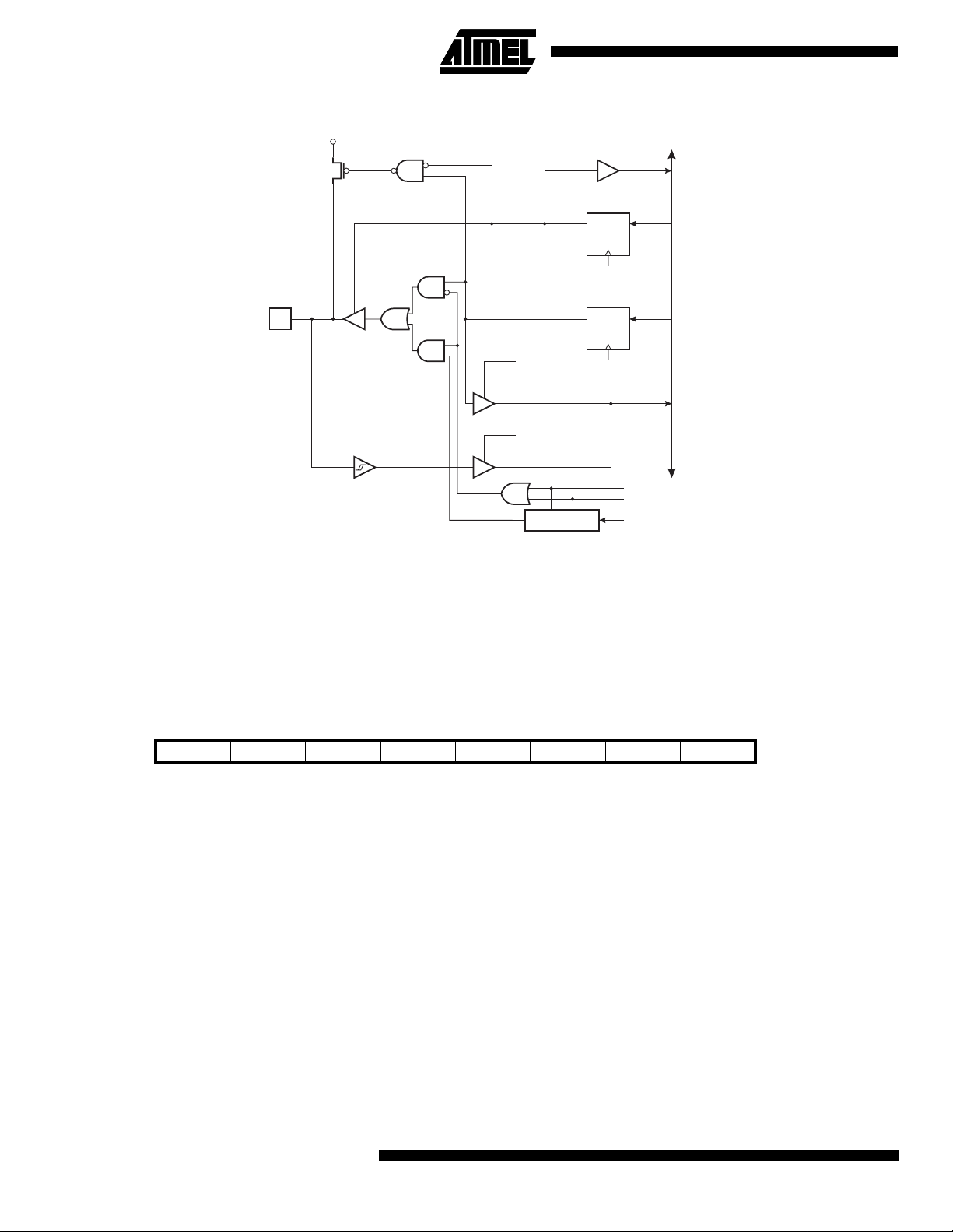
Figure 60. Port B Schematic Diagram (Pin PB7)
MOS
PULLUP
PB7
RD
RESET
R
D
Q
DDB7
C
WD
RESET
R
Q
D
PORTB7
C
RL
RP
WP
DATA BUS
WRITE PORTB
WP:
WRITE DDRB
WD:
READ PORTB LATCH
RL:
READ PORTB PIN
RP:
READ DDRB
RD:
OUTPUT
MODE SELECT
COM20
COM21
COMP. MATCH 2
Port C
PORT C is an 8-bit Output port.
The Port C pins hav e altern ate fun ction s relat ed to th e opti onal exter nal da ta SRA M. Wh en us ing th e devic e with externa l
SRAM, Port C outputs the high-order address byte during accesses to external data memory. When a reset condition
becomes active, the port pins are not tristated, but the pins will assume their initial value after two stable clock cycles.
The Port C Data Register - PORTC
Bit 76543210
$15 ($35) PORTC7 PORTC6 PORTC5 PORTC4 PORTC3 PORTC2 PORTC1 PORTC0 PORTC
Read/Write R/W R/W R/W R/W R/W R/W R/W R/W
Initial value00000000
82
ATmega603/103
Page 83
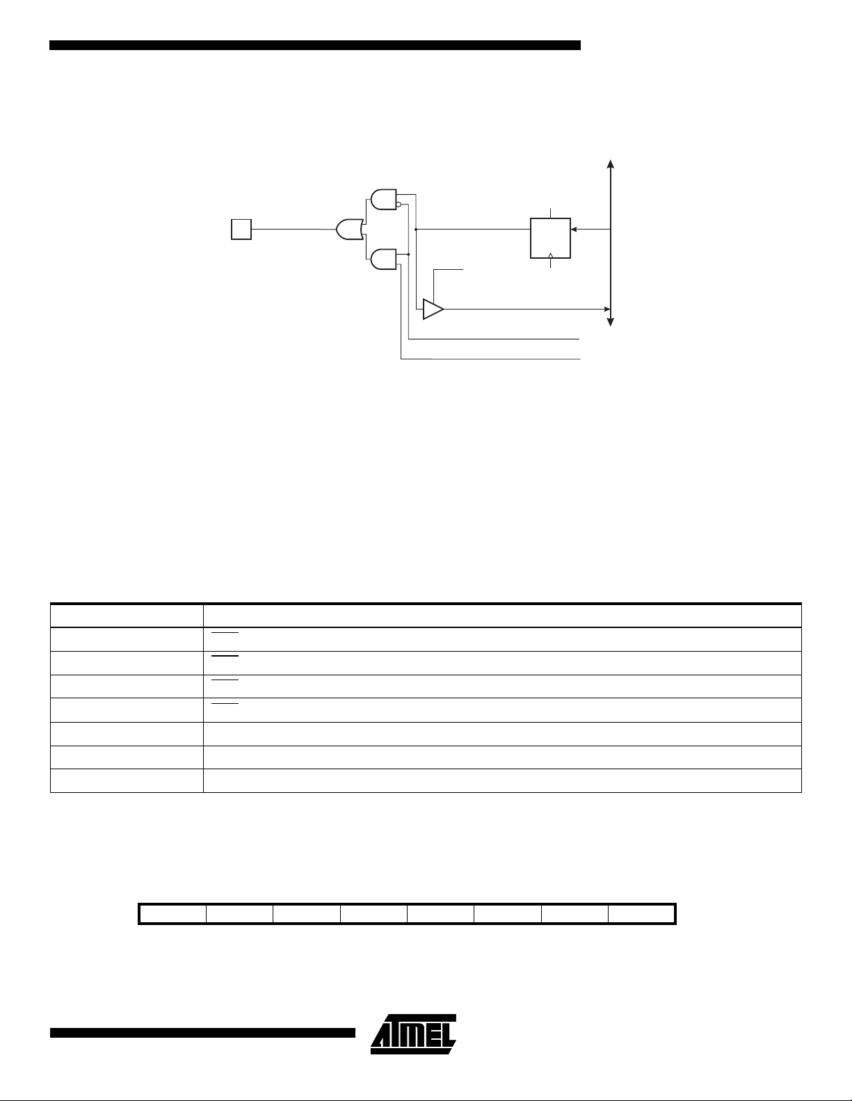
ATmega603/103
US
Port C Schematics
Figure 61. Port C Schematic Diagram (Pins PC0 - PC7)
RESET
R
Q
PCn
WRITE PORTC
WP:
READ PORTC LATCH
RL:
SRAM ADDRESS
A:
EXTERNAL SRAM ENABLE
SRE:
0-7
n:
RL
PORTCn
C
WP
D
Port D
Port D is an 8 bit bi-directional I/O port with internal pull-up resistors.
Three I/O memory address locations are allocated for the Port D, one each for the Data Register - PORTD, $12($32), Data
Direction Register - DDRD, $11($31) and the Port D Input Pins - PIND, $10($30). The Port D Input Pins address is read
only, while the Data Register and the Data Direction Register are read/write.
The Port D output buffers can sink 20 mA. As inputs, Port D pins that are externally pulled low will source current if the pullup resistors are activated.
Some Port D pins have alternate functions as shown in the following table:
DATA B
SRE
An
Table 32. Port D Pins Alternate Functions
Port Pin Alternate Function
PD0 INT0 (External Interrupt0 Input)
PD1 INT1
PD2 INT2
(External Interrupt1 Input)
(External Interrupt2 Input)
PD3 INT3 (External Interrupt3 Input)
PD4 IC1 (Timer/Counter1 Input Capture Trigger)
PD6 T1 (Timer/Counter1 Clock Input)
PD7 T2 (Timer/Counter2 Clock Input)
When the pins are used for the alternate function the DDRD and PORTD register has to be set according to the alt ernate
function description.
Port D Data Register - PORTD
Bit 76543210
$12 PORTD7 PORTD6 PORTD5 PORTD4 PORTD3 PORTD2 PORTD1 PORTD0 PORTD
Read/Write R/W R/W R/W R/W R/W R/W R/W R/W
Initial value00000000
83
Page 84
Port D Data Direction Register - DDRD
Bit 76543210
$11 DDD7 DDD6 DDD5 DDD4 DDD3 DDD2 DDD1 DDD0 DDRD
Read/Write R/W R/W R/W R/W R/W R/W R/W R/W
Initial value00000000
Port D Input Pins Address - PIND
Bit 76543210
$10 PIND7 PIND6 PIND5 PIND4 PIND3 PIND2 PIND1 PIND0 PIND
Read/WriteRRRRRRRR
Initial value Hi-Z Hi-Z Hi-Z Hi-Z Hi-Z Hi-Z Hi-Z Hi-Z
The Port D Input Pins address - PIND - is not a register, and this address enables access to the physical value on each
Port D pin. When reading PORTD, the Port D Data Latch is read, and when reading PIND, the logical values present on the
pins are read.
Port D as general digital I/O
PDn, General I/O pin: The DDDn bit in the DDRD register selects the direction of this pin. If DDDn is set (one), PDn is configured as an outpu t pin. If DDDn is c leared (zero), PDn is con figur ed as an inpu t pin. If PDn is s et (one ) when conf igured
as an input pin t he MO S pu ll up resi stor i s ac tivated. To swi tch the pu ll up resi stor off th e PDn has to be clear ed ( zero) or
the pin has to be configured as an output pin.The port pins are tri-stated when a reset condition becomes active, even if the
clock is not running.
Table 33. DDDn Bits on Port D Pins
DDDn PORTDn I/O Pull up Comment
0 0 Input No Tri-state (Hi-Z)
0 1 Input Yes PDn wi ll source curr ent if ext. pulled low.
1 0 Output No Push-Pull Zero Output
1 1 Output No Push-Pull One Output
Note: n: 7,6...0, pin number
Alternate Functions of Port D
.. INT3 - Port D, Bits 0..3
INT0
External Interrupt sources 0 - 3. The PD0 - PD3 pins can serve as external active low interrupt sources to the MCU. The
internal pull up MOS resistors can be activated as described above. See the interrupt description for further details, and
how to enable the sources.
IC1 - Port D, Bit 4
IC1 - Input Capture pin for Timer/Counter1. When a positive or negative (selectable) edge is applied to this pin, the contents of Timer/Counter1 is transferred to the Timer/Counter1 Input Capture Register. The pin has to be configured as an
input to serve th is f unction. See the Tim er/Co unter1 d escri ption on ho w to o perat e this functi on. The inter nal pull up M OS
resistor can be activated as described above.
T1 - Port D, Bit 6
T1, Timer/Counter1 counter source. See the timer description for further details.
T2 - Port D, Bit 7
T2, Timer/Counter2 counter source. See the timer description for further details.
84
ATmega603/103
Page 85
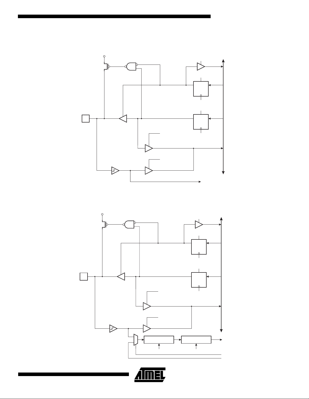
ATmega603/103
Port D Schematics
Note that all port pins are synchronized. The synchronization latches are however, not shown in the figures.
Figure 62. Port D Schematic Diagram (Pins PD0, PD1, PD2 and PD3)
RD
MOS
PULLUP
RESET
R
D
Q
DDDn
C
WD
RESET
PDn
R
D
Q
PORTDn
C
RL
RP
WP
DATA BUS
WRITE PORTD
WP:
WRITE DDRD
WD:
READ PORTD LATCH
RL:
READ PORTD PIN
RP:
READ DDRD
RD:
0, 1, 2, 3
n:
Figure 63. Port D Schematic Diagram (Pin PD4)
MOS
PULLUP
PD4
INTn
RD
RESET
R
D
Q
DDD4
C
WD
RESET
R
D
Q
PORTD4
C
RL
RP
WP
DATA BUS
WRITE PORTD
WP:
WRITE DDRD
WD:
READ PORTD LATCH
RL:
READ PORTD PIN
RP:
READ DDRD
RD:
COMPARATOR IC ENABLE
ACIC:
COMPARATOR OUTPUT
ACO:
0
NOISE CANCELER EDGE SELECT ICF1
1
ICNC1 ICES1
ACIC
ACO
85
Page 86
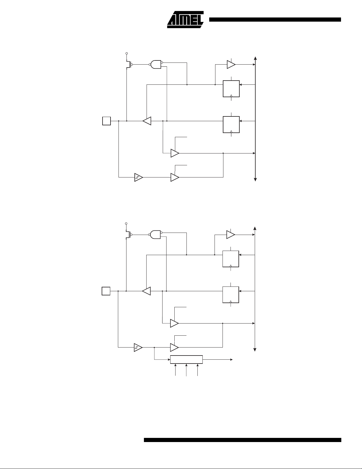
Figure 64. Port D Schematic Diagram (Pin PD5)
MOS
PULLUP
PD5
WP:
WRITE PORTD
WD:
WRITE DDRD
RL:
READ PORTD LATCH
RP:
READ PORTD PIN
RD:
READ DDRD
Figure 65. Port D Schematic Diagram (Pins PD6 and PD7)
MOS
PULLUP
PDn
RD
RESET
R
D
Q
DDD5
C
WD
RESET
R
D
Q
PORTD5
C
RL
RP
RL
WP
RD
RESET
Q
DDDn
WD
RESET
Q
PORTDn
WP
R
D
C
R
D
C
DATA BUS
DATA BUS
86
WRITE PORTD
WP:
WRITE DDRD
WD:
READ PORTD LATCH
RL:
READ PORTD PIN
RP:
READ DDRD
RD:
6, 7
n:
1, 2
m:
ATmega603/103
RP
SENSE CONTROL
CSm2
CSm1
CSm0
TIMERm CLOCK
SOURCE MUX
Page 87
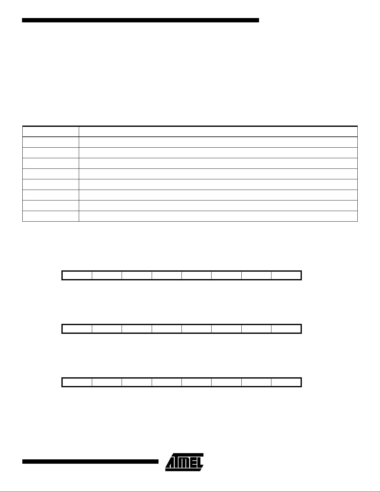
ATmega603/103
Port E
Port E is an 8-bit bi-directional I/O port with internal pull-up resistors.
Three I/O memory address locations are allocated for the Port E, one each for the Data Register - PORTE, $03($23), Data
Direction Register - DDRE, $02($22) and the Port E Input Pins - PINE, $01($21). The Port E Input Pins address is read
only, while the Data Register and the Data Direction Register are read/write.
The Port E output buffers can sink 20 mA. As inputs, Port E pins that are externally pulled low will source current if the pullup resistors are activated.
All Port E pins have alternate functions as shown in the following table:
Table 34. Port E Pins Alternate Functions
Port Pin Alternate Function
PE0 PDI/RXD (Programming Data Input or UART Receive Pin)
PE1 PDO/TXD (Programming Data Output or UART Transmit Pin)
PE2 AC+ (Analog Comparator Positive Input)
PE3 AC- (Analog Comparator Negative Input)
PE4 INT4 (External Interrupt4 Input)
PE5 INT5 (External Interrupt5 Input)
PE6 INT6 (External Interrupt6 Input)
PE7 INT7 (External Interrupt7 Input)
When the pins are used for the altern ate function th e DDRE and POR TE register has to be set accordi ng to the alte rnate
function description.
Port E Data Register - PORTE
Bit 76543210
$03 ($23) PORTE7 PORTE6 PORTE5 PORTE4 PORTE3 PORTE2 PORTE1 PORTE0 PORTE
Read/Write R/W R/W R/W R/W R/W R/W R/W R/W
Initial value00000000
Port E Data Direction Register - DDRE
Bit 76543210
$02 ($22) DDE7 DDE6 DDE5 DDE4 DDE3 DDE2 DDE1 DDE0 DDRE
Read/Write R/W R/W R/W R/W R/W R/W R/W R/W
Initial value00000000
Port E Input Pins Address - PINE
Bit 76543210
$01 ($21) PINE7 PINE6 PINE5 PINE4 PINE3 PINE2 PINE1 PINE0 PINE
Read/WriteRRRRRRRR
Initial value Hi-Z Hi-Z Hi-Z Hi-Z Hi-Z Hi-Z Hi-Z Hi-Z
The Port E Input Pins address - PINE - is not a register, and this address enables access to the physical value on each Port
E pin. When reading PORTE, the Port E Data Latch is read, and when reading PINE, the logical values present on the pins
are read.
87
Page 88

Port E as general digital I/O
PEn, General I/O pin: The DDEn bit in the DDRE regi ste r selects the di recti on o f this pin. If DDE n is set (one), PE n i s configured as an output pin. If DDEn is cleared (zero), PEn is configured as an input pin. If PEn is set (one) when configured as
an input pin, the MOS pull up res istor is activ ate d. To s witc h the pul l up res istor off the PE n ha s to be cl eared (zer o) or the
pin has to be configured as an output pin.The port pins are tri-stated when a reset condition becomes active, even if the
clock is not running.
Table 35. DDEn Bits on Port E Pins
DDEn PORTEn I/O Pull up Comment
0 0 Input No Tri-state (Hi-Z)
0 1 Input Yes PDn will source current if ext. pulled low.
1 0 Output No Push-Pull Zero Output
1 1 Output No Push-Pull One Output
Note: n: 7,6...0, pin number
Alternate Functions OF Port E
PDI/RXD - Port E, Bit 0
PDI, Serial Programming Data Input. During Serial Program Downloading, this pin is used as data input line for the
ATmega603/103.
RXD, UART Receive Pin. Receive Data (Data input pin for the UART). When the UART receiver is enabled this pin is configured as an input regardless of the value of DDRD0. When the UART forces this pin to be an input, a logical one in
PORTD0 will turn on the internal pull-up.
PDO/TXD - Port E, Bit 1
PDO, Serial Programming Data Output. During Serial Program Downloadi ng, this pin is used as data output line for the
ATmega603/103.
TXD, UART Transmit Pin.
AC+ - Port E, Bit 2
AC+ - Analog Comparator Positive Input. This pin is directly connected to the positive input of the analog comparator.
AC- - Port E, Bit 3
AC- - Analog Comparator Negative Input. This pin is directly connected to the negative input of the analog comparator.
INT4 .. INT7 - Port E, Bit 4-7
INT4 .. INT7 - External Interrupt sources 4 - 7: The PE4 - PE7 pins can serve as external interrupt sources to the MCU.
Interrupts can be tr igger ed by low l evel o r posit ive or nega tive e dge on these p ins. The i nternal p ull u p MOS res istors can
be activated as described above. See the interrupt description for further details, and how to enable the sources.
Port E Schemati cs
Note that all port pins are synchronized. The synchronization latches are however, not shown in the figures.
88
ATmega603/103
Page 89

Figure 66. Port E Schematic Diagram, Pin PE0
ATmega603/103
Figure 67. Port E Schematic Diagram (Pin PE1)
89
Page 90

Figure 68. Port E Schematic Diagram (Pin PE2)
MOS
PULLUP
PE2
RD
RESET
D
Q
DDE2
C
WD
RESET
D
Q
PORTE2
C
RL
RP
WP
DATA BUS
WP:
WRITE PORTE
WD:
WRITE DDRE
RL:
READ PORTE LATCH
RP:
READ PORTE PIN
RD:
READ DDRE
Figure 69. Port E Schematic Diagram (Pin PE3)
MOS
PULLUP
PE3
TO COMPARATOR
RD
RESET
D
Q
DDE3
C
WD
RESET
D
Q
PORTE3
C
RL
RP
WP
AC+
DATA BUS
90
WP:
WRITE PORTE
WD:
WRITE DDRE
RL:
READ PORTE LATCH
RP:
READ PORTE PIN
RD:
READ DDRE
ATmega603/103
TO COMPARATOR
AC-
Page 91

Figure 70. Port E Schematic Diagram (Pins PE4, PE5, PE6 and PE7)
MOS
PULLUP
PEn
RL
RP
WRITE PORTE
WP:
WRITE DDRE
WD:
READ PORTE LATCH
RL:
READ PORTE PIN
RP:
READ DDRE
RD:
4, 5, 6, 7
n:
SENSE CONTROL INTn
ISCn1 ISCn0
RD
RESET
Q
DDEn
WD
RESET
Q
PORTEn
WP
ATmega603/103
R
D
C
R
D
C
DATA BUS
Port F
Port F is an 8-bit input port.
One I/O memory location is allocated for Port F, the Port F Input Pins - PINF, $00 ($20).
All Port F pins are connected to the analog multiplexer which further is connected to the A/D converter. The digital input
function of Port F can be used together wi th the A/D converter, allowi ng the user to use s ome pins of Port F and digital
inputs and other as analog inputs, at the same time.
Port F Input Pins Address - PINF
Bit 76543210
$00 ($20) PINF7 PINF6 PINF5 PINF4 PINF3 PINF2 PINF1 PINF0 PINF
Read/WriteRRRRRRRR
Initial value Hi-Z Hi-Z Hi-Z Hi-Z Hi-Z Hi-Z Hi-Z Hi-Z
The Port F Input Pins address - PINF - is not a register, and this address enables access to the physical value on each Port
F pin.
91
Page 92

Figure 71. Port F Schematic Diagra m (Pins PF7 - PF0)
US
PFn
RP
DATA B
RP:n:READ PORTF PIN
0 - 7
TO ADC MUX
AINn
Memory Programming
Program and Data Memory Lock Bits
The ATmega603/103 MCU provide s two Lock bits which can be left unprogrammed (‘1’) or can be programmed (‘0’) to
obtain the additional features listed in Table 36. The Lock bits can only be erased to ‘1’ with the Chip Erase command..
Table 36. Lock Bit Protection Modes
Memory Lock Bits Protection Type
Mode LB1 LB2
1 1 1 No memory lock features enabled.
2 0 1 Further programming of the Flash and EEPROM is disabled.
3 0 0 Same as mode 2, and verify is also disabled.
Note: 1. In Parallel mode, programming of the Fuse bits are also disabled. Program the Fuse bits before programming the Lock bits.
Fuse Bits
The ATmega603/103 has four Fuse bits, SPIEN, SUT1..0, and EESAVE.
• When the SPIEN Fuse is programmed (‘0’), Serial Program and Data Downloading is enabled. Default value is
programmed (‘0’). The SPIEN Fuse is not accessible in serial programming mode.
• When EESAVE is programmed, the EEPROM memory is preserved through the Chip Erase cycle. Default value is
unprogrammed (‘1’). The EESAVE Fuse bit can not be programmed if any of the Lock bits are programmed.
• SUT1..0 Fuses: Determine the MCU start-up time. See Table 6 on page 26 for further details. Default value is unprogrammed (‘11’), which gives a nominal start up time of 16 ms.
The status of the Fuse bits is not affected by Chip Erase.
(1)
92
ATmega603/103
Page 93

ATmega603/103
Signature Bytes
All Atmel microcontrollers have a three-byte signature code which identifies the device. This code can be read in both serial
and parallel mode. The three bytes reside in a separate address space.
For the ATmega603 they are:
1. $000: $1E (indicates manufactured by Atmel)
2. $001: $96 (indicates 64 Kb Flash memory)
3. $002: $01 (indicates ATmega603 when signature byte $001 is $96)
For the ATmega103 they are:
1. $000: $1E (indicates manufactured by Atmel)
2. $001: $97 (indicates 128 Kb Flash memory)
3. $002: $01 (indicates ATmega103 when signature byte $001 is $97)
Programming the Flash and EEPROM
Atmel’s ATmega603/103 offers 64K/128K bytes of in-system reprogrammable Flash memory and 2K/4K bytes of EEPROM
Data memory.
The ATmega603/103 is shipped with the on-chip Flash Program and EEPROM Data memory arrays in the erased state
(i.e. contents = $FF) and ready to be programmed. This device supports a High-Voltage (12V) Parallel programming mode
and a Low-Voltage Ser ial pro grammin g mo de. The + 12V supp lied i s used fo r progr ammi ng enab le onl y, and no c urrent of
significance is dr awn by thi s pin. The serial programmi ng mod e p ro vides a co nv eni ent way to dow nlo ad p r ogram and data
into the ATmega603/103 inside the user’s system.
The Flash Program memory array on the ATmega603/103 is organized as 256/512 pages of 256 bytes each. When programming the Fla sh, the program dat a is latched into a pag e buffer. This allow s one page of program data to be
programmed simultaneously in either programming mode.
The EEPROM Data memory array on the ATmega603/103 is programmed byte-by-byte in either programming mode. An
auto-erase cycle is provided within the self-timed EEPROM write instruction in the serial programming mode.
During programming, the supply voltage must be in accordance with Table 37
Table 37. Supply voltage during programming
Part Serial programming Parallel programming
ATmega103/603 4.0 - 5.0 V 4.0 - 5.0 V
ATmega103L/603L 3.4 - 3.6 V 3.4 - 5.0 V
Parallel Programming
This section describes how to paral lel program and verify Flash Prog ram memory, EEPR OM Data mem ory, Lock bits and
Fuse bits in the ATmega603/103. Pulses are assumed to be at least 500 ns unless otherwise noted.
Signal Names
In this section, so me pins of th e ATmega6 03/103 ar e refere nced by signal nam es describ ing thei r funct ion durin g paralle l
programming, see Figure 72 and Table 38. Pins not described in Table 38 are referenced by pin names.
The XA1/XA0 pins determine the ac tion ex ecuted when the XTAL 1 pin is given a positive pulse. The bi t coding are shown
in Table 39.
When pulsing WR
ent bits are assigned functions as shown in Table 40.
or OE, the command l oaded de termines the actio n exec uted. The Co mmand i s a byte whe re the di ffer-
93
Page 94

Figure 72. Parallel Programming
ATmega603(L),
ATmega103(L)
RDY/BSY
OE
WR
BS1
XA0
XA1
PAGEL
.
PD1
PD2
PD3
PD4
PD5
PD6
PA0
RESET+12V
PD7
XTAL1
GND
Table 38. Pin Name Mapping
Signal Name in Programming Mode Pin Name I/O Function
RDY/BSY PD1 O 0: Device is busy programming, 1: Device is ready for new command
+5V
VCC
PB7 - PB0 DATA
OE
WR
PD2 I Output Enable (Active low)
PD3 I Write Pulse (Active low)
BS1 PD4 I Byte Select 1 (‘0’ selects low byte, ‘1’ selects high byte)
XA0 PD5 I XTAL Action Bit 0
XA1 PD6 I XTAL Action Bit 1
BS2 PD7 I Byte Select 2 (Always low)
PAGEL PA0 I Program Memory Page Load
DATA PB7-0 I/O Bidirectional Data bus (Output when OE
Table 39. XA1 and XA0 Coding
XA1 XA0 Action when XTAL1 is Pulsed
0 0 Load Flash or EEPROM Address (High or low address byte determined by BS1)
0 1 Load Data (High or Low data byte for Flash determined by BS1)
1 0 Load Command
1 1 No Action, Idle
is low)
94
ATmega603/103
Page 95

Table 40. Command Byte Bit Coding
Command Byte Command Executed
1000 0000 Chip Erase
0100 0000 Write Fuse Bits
0010 0000 Write Lock Bits
0001 0000 Write Flash
0001 0001 Write EEPROM
0000 1000 Read Signature Bytes
0000 0100 Read Lock and Fuse Bits
0000 0010 Read Flash
0000 0011 Read EEPROM
Enter Programming Mode
The following algorithm puts the device in parallel programming mode:
1. Apply supply voltage according to Table 37, between V
2. Set RESET
3. Apply 11.5 - 12.5V to RESET
and BS1 pins to ‘0’ and wait at least 100 ns.
. Any activity on BS1 within 100 ns after +12V has been applied to RESET, will cause
and GND.
CC
the device to fail entering programming mode.
ATmega603/103
Chip Erase
The Chip Erase will erase the Flas h and EEP ROM me mories , and Lock bi ts. The Loc k bits are not reset un til the prog ram
memory has been completely erased. The Fuse bits are not changed. A chip erase must be performed before the Flash or
EEPROM is reprogrammed.
Load Command “Chip Erase”
1. Set XA1, XA0 to ‘10’. This enables command loading.
2. Set BS1 to ‘0’.
3. Set DATA to ‘1000 0000’. This is the command for Chip erase.
4. Give XTAL1 a positive pulse. This loads the command.
5. Give WR
a t
WLWH_CE
not generate any activity on the RDY/BSY
wide negative pulse to execute Chip Erase. See Table 41 for t
pin.
WLWH_CE
value. Chip Erase does
Table 41. Minimum WR pulse width for chip erase
Symbol 3.2V 3.6V 4.0V 5.0V
t
WLWH_CE
56 ms 43 ms 35 ms 22 ms
95
Page 96

Programming The Flash
The Flash is organized as 256/512 pages of 256 bytes each. When programming the Flash, the program data is latched
into a page buffer. This allows one page of program data to be programmed simultaneously. The following procedure
describes how to program the entire Flash memory:
A: Load Command “Write Flash”
1. Set XA1, XA0 to ‘10’. This enables command loading.
2. Set BS1 to ‘0’
3. Set DATA to ‘0001 0000’. This is the command for Write Flash.
4. Give XTAL1 a positive pulse. This loads the command.
B: Load Address Low Byte
1. Set XA1, XA0 to ‘00’. This enables address loading.
2. Set BS1 to ‘0’. This selects low address.
3. Set DATA = Address low byte ($00 - $FF)
4. Give XTAL1 a positive pulse. This loads the address low byte.
C: Load Data Low Byte
1. Set BS1 to ‘0’. This selects low data.
2. Set XA1, XA0 to ‘01’. This enables data loading.
3. Set DATA = Data low byte ($00 - $FF)
4. Give XTAL1 a positive pulse. This loads the data byte.
D: Latch Data Low byte
Give PAGEL a positive pulse, This latches the data low byte.
(See Figure 73 for signal waveforms.)
E: Load Data High Byte
1. Set BS1 to ‘1’. This selects high data.
2. Set XA1, XA0 to ‘01’. This enables data loading.
3. Set DATA = Data high byte ($00 - $FF)
4. Give XTAL1 a positive pulse. This loads the data high byte.
F: Latch Data High Byte
Give PAGEL a positive pulse. This latches the data high byte.
G: Repeat B through F 128 times to fill the page buffer
H: Load Address High Byte
1. Set XA1, XA0 to ‘00’. This enables address loading.
2. Set BS1 to ‘1’. This selects high address.
3. Set DATA = Address high byte ($00-$7F/$FF).
4. Give XTAL1 a positive pulse. This loads the address high byte.
I: Program Page
1. Give WR
2. Wait until RDY/BSY
(See Figure 74 for signal waveforms.)
J: End Page Programming
1. Set XA1, XA0 to ‘10’. This enables command loading.
2. Set DATA = ‘0000 0000’. This is the command for No Operation.
3. Give XTAL1 a positive pulse. This loads the command and the internal write signals are reset.
a negative pulse. This starts programming of the entire page of data. RDY/BSY goes low.
goes high.
96
ATmega603/103
Page 97
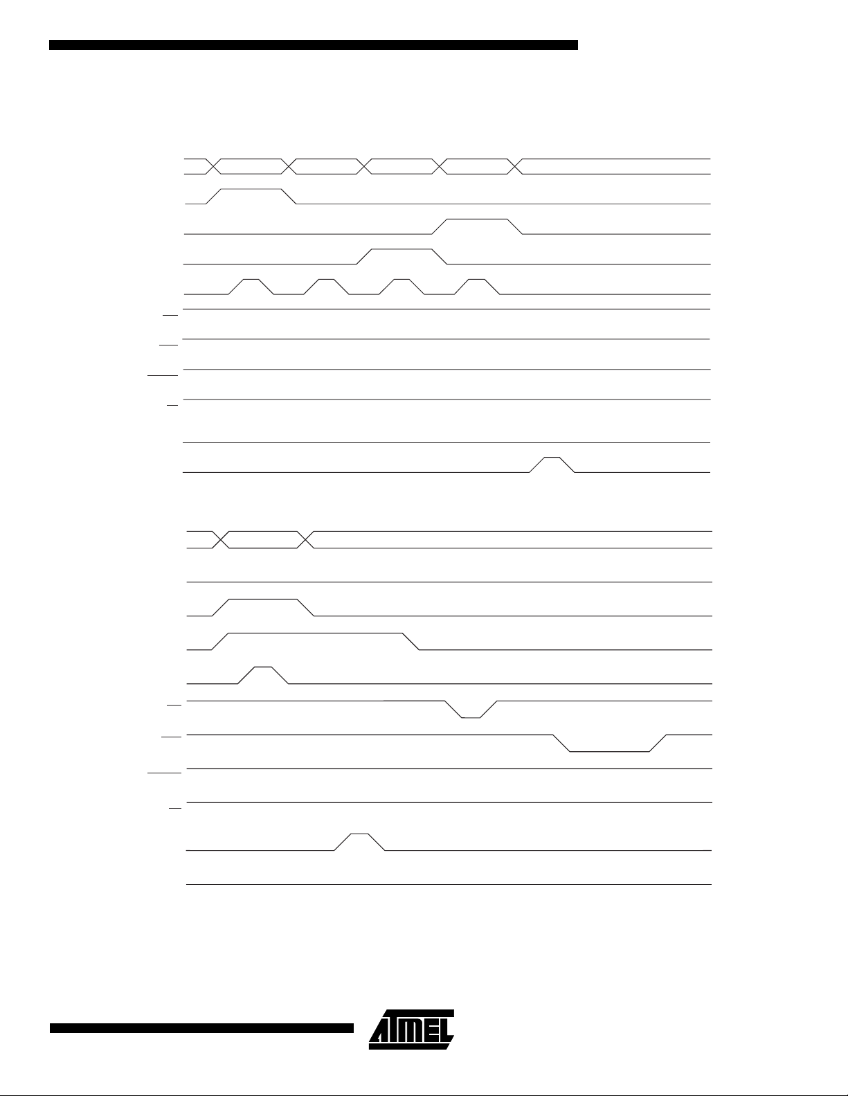
K: Repeat A through J 256/512 times or until all data have been programmed.
Figure 73. Programming the Flash waveforms
$10 ADDR. LOW ADDR. HIGH DATA LOWDATA
XA1
XA2
BS1
XTAL1
WR
RDY/BSY
+12V
RESET
OE
BS2
ATmega603/103
PAGEL
Figure 74. Programming the Flash waveforms (continued)
DATA
XA1
XA0
BS1
XTAL1
WR
RDY/BSY
RESET
OE
PAGEL
DATA HIGH
+12V
BS2
97
Page 98

Programming The EEPROM
The programming algor ithm for th e EEPRO M data mem ory is a s follows ( refer to P rogramming the Flash for details on
Command, Address and Data loading):
1. A: Load Command ‘0001 0001’.
2. H: Load Address High Byte ($00-$07/$0F)
3. B: Load Address Low Byte ($00 - $FF)
4. E: Load Data Low Byte ($00 - $FF)
L: Write Data Low Byte
1. Set BS to ‘0’. This selects low data.
2. Give WR
3. Wait until RDY/BSY
a negative pulse. This starts programming of the data byte. RDY/BSY goes low.
goes high to program the next byte.
(See Figure 75 for signal waveforms.)
The loaded command and address are retained in the device during programming. For efficient programming, the following
should be considered.
• The command needs only be loaded once when writing or reading multiple memory locations.
• Address high byte needs only be loaded before programming a new 256 word page in the EEPROM.
• Skip writing the data value $FF, that is the contents of the entire EEPROM after a Chip Erase.
These considerations also applies to Flash, EEPROM and Signature bytes reading.
Figure 75. Programming the EEPROM waveforms
XA1
XA2
BS1
XTAL1
WR
RDY/BSY
RESET
OE
BS2
PAGEL
$11 ADDR. HIGH ADDR. LOW DATA LOWDATA
+12V
98
ATmega603/103
Page 99

ATmega603/103
Readin g Th e Fl a sh
The algorithm for reading the Flash memory is as fo llows (refer to Programming the Flash for details on Command and
Address loading):
1. A: Load Command ‘0000 0010’.
2. H: Load Address High Byte ($00-$7F/$FF)
3. B: Load Address Low Byte ($00 - $FF)
4. Set OE
5. Set BS to ‘1’. The Flash word high byte can now be read at DATA
6. Set OE
Reading The EEPROM
The algorithm for reading the EEPROM memory is as follows (refer to Programming the Flash for details on Command and
Address loading):
1. A: Load Command ‘0000 0011’.
2. H: Load Address High Byte ($00-$07/$0F)
3. B: Load Address ($00 - $FF)
4. Set OE
5. Set OE
to ‘0’, and BS1 to ‘0’. The Flash word low byte can now be read at DATA
to ‘1’.
to ‘0’, and BS1 to ‘0’. The EEPROM Data byte can now be read at DATA
to ‘1’.
Programming The Fuse Bits
The algorithm for programming the Fuse bits is as follows (refer to Programming the Flash for details on Command and
Data loading):
1. A: Load Command ‘0100 0000’.
2. C: Load Data Low Byte. Bit n = ‘0’ programs and bit n = ‘1’ erases the Fuse bit.
Bit 5 = SPIEN Fuse bit
Bit 3 = EESAVE Fuse bit
Bit 2 = always ‘1’
Bit 1 = SUT1 Fuse bit
Bit 0 = SUT0 Fuse bit
Bit 7, 6,4,2 = ‘1’. These bits are reserved and should be left unprogrammed (‘1’).
3. Give WR
the Fuse bits does not generate any activity on the RDY/BSY
Programming the Lock Bits
The algorithm for programming the Lock bits is as follows (refer to Programming the Flash for details on Command and
Data loading):
1. A: Load Command ‘0010 0000’.
2. D: Load Data Low Byte. Bit n = ‘0’ programs the Lock bit.
Bit 2 = Lock Bit2
Bit 1 = Lock Bit1
Bit 7-3,0 = ‘1’. These bits are reserved and should be left unprogrammed (‘1’).
3. L: Write Data Low Byte.
The Lock bits can only be cleared by executing Chip Erase.
a t
WLWH_PFB
wide negative pulse to execute the programming, t
pin.
WLWH_PFB
is found in Table 42. Programming
99
Page 100

Reading the Fuse and Lock Bits
The algorithm for reading the Fuse and Lock bits is as follows (refer to Programming the Flash for details on Command
loading):
1. A: Load Command ‘0000 0100’.
2. Set OE
to ‘0’, and BS to ‘0’. The status of the Fuse bits can now be read at DATA (‘0’ means programmed).
Bit 5 = SPIEN Fuse bit
Bit 3 = EESAVE Fuse bit
Bit 1 = SUT1 Fuse bit
Bit 0 = SUT0 Fuse bit
Set OE
to ‘0’, and BS to ‘1’. The status of the Lock bits can now be read at DATA (‘0’ means programmed).
Bit 2 = Lock Bit2
Bit 1 = Lock Bit1
3. Set OE
to ‘1’.
Reading the Signature Bytes
The algorithm for reading the Signature bytes is as follows (refer to Programming the Flash for details on Command and
Address loading):
1. A: Load Command ‘0000 1000’.
2. C: Load Address Low Byte ($00 - $02).
Set OE
3. Set OE
to ‘0’, and BS to ‘0’. The selected Signature byte can now be read at DATA.
to ‘1’.
Parallel Programming Characteristics
Figure 76. Parallel Programming Timing
XTAL1
t
Data & Contol
(DATA, XA0/1, BS1)
PAGEL
WR
RDY/BSY
OE
DATA
DVXH
t
BVXH
t
XHXL
t
PHPL
t
XLWL
t
XLDX
t
PLBX
t
PLWL
t
XLOL
t
BVWL
t
WLWH
t
OLDV
t
WHRL
t
RHBX
t
WLRH
t
OHDZ
Write
Read
100
ATmega603/103
 Loading...