

Page 1
Features
• 3.0V to 3.6V Operating Range
• Advanced, High-speed, Electrically-erasable Programmable Logic Device
– Superset of 22V10
– Enhanced Logic Flexibility
– Architecturally Compatible with ATV750B and ATV750 Software and Hardware
• D- or T-type Flip-flop
• Product Term or Direct Input Pin Clocking
• 15 ns Maximum Pin-to-pin Delay with 3V Operation
• Highest Density Programmable Logic Available in 24-pin Package
– Advanced Electrically-erasable Technology
– Reprogrammable
– 100% Tested
• Increased Logic Flexibility
– 42 Array Inputs, 20 Sum Terms and 20 Flip-flops
• Enhanced Output Logic Flexibility
– All 20 Flip-flops Feed Back Internally
– 10 Flip-flops are also Available as Outputs
• Programmable Pin-keeper Circuits
• Dual-in-line and Surface Mount Package in Standard Pinouts
• Commercial and Industrial Temperature Ranges
• 20-year Data Retention
• 2000V ESD Protection
• 1000 Erase/Write Cycles
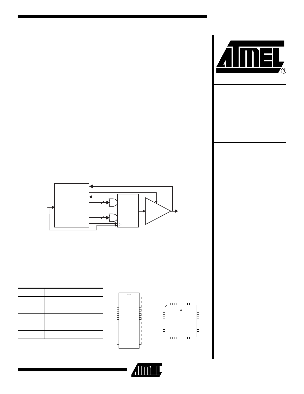
Block Diagram
High-speed
Complex
Programmable
Logic Device
ATF750LVC
(OE PRODUCT TERMS)
12
INPUT
PINS
PROGRAMMABLE
INTERCONNECT
AND
COMBINATORIAL
LOGIC ARRAY
4TO8
PRODUCT
TERMS
(CLOCK PIN)
LOGIC
OPTION
(UP T0 20
FLIP-FLOPS)
OUTPUT
OPTION
10
I/O
PINS
Description
The Atmel “750” architecture is twice as powerful as most other 24-pin programmable
logic devices. Increased product terms, sum terms, flip-flops and output logic configurations translate into more usable gates. High-speed logic and uniform, predictable
delays guarantee fast in-system performance. The ATF750LVC is a high-performance
(continued)
Pin Configurations
Pin Name Function
CLK Clock
IN Logic Inputs
I/O Bi-directional Buffers
GND Ground
VCC 3V Supply
Note: For PLCC, pins 1, 8, 15, and 22
can be left unconnected. For
superior performance, connect
VCC to pin 1 and GND to pins
8, 15, and 22.
DIP/SOIC/TSSOP
CLK/IN
GND
1
2
IN
3
IN
4
IN
5
IN
6
IN
7
IN
8
IN
9
IN
10
IN
11
IN
12
24
23
22
21
20
19
18
17
16
15
14
13
VCC
I/O
I/O
I/O
I/O
I/O
I/O
I/O
I/O
I/O
I/O
IN
GND *
IN
IN
IN
IN
IN
IN
PLCC
ININCLK/IN
VCC *
432
5
6
7
8
9
10
11
1
12131415161718
IN
IN
GND
GND *
VCC
I/O
282726
IN
I/O
I/O
I/O
25
I/O
24
I/O
23
GND *
22
I/O
21
I/O
20
I/O
19
I/O
Rev. 1447D–03/01
1
Page 2
CMOS (electrically-erasable) complex programmable logic
device (CPLD) that utilizes Atmel’s proven electrically-erasable technology.
Each of the ATF750LVC’s 22 logic pins can be used as an
input. Ten of these can be used as inputs, outputs or bidirectional I/O pins. Each flip-flop is individually configurable as either D- or T-type. Each flip-flop output is fed
back into the array independently. This allows burying of all
the sum terms and flip-flops.
There are 171 total product terms available. There are two
sum terms per output, providing added flexibility. A variable
format is used to assign between four to eight product
Absolute Maximum Ratings*
Temperature Under Bias.................................. -40°C to +85°C
Storage Temperature ..................................... -65°C to +150°C
Voltage on Any Pin with
Respect to Ground .........................................-2.0V to +4.6V
Voltage on Input Pins
with Respect to Ground
During Programming.....................................-2.0V to +14.0V
Programming Voltage with
Respect to Ground .......................................-2.0V to +14.0V
(1)
(1)
(1)
terms per sum term. Much more logic can be replaced by
this device than by any other 24-pin PLD. With 20 sum
terms and flip-flops, complex state machines are easily
implemented with logic to spare.
Product terms provide individual clocks and asynchronous
resets for each flip-flop. Each flip-flop may also be individually configured to have direct input pin controlled clocking.
Each output has its own enable product term. One product
term provides a common synchronous preset for all flipflops. Register preload functions are provided to simplify
testing. All registers automatically reset upon power-up.
*NOTICE: Stresses beyond those listed under “Absolute
Maximum Ratings” may cause permanent damage to the device. This is a stress rating only and
functional operation of the device at these or any
other conditions beyond those indicated in the
operational sections of this specification is not
implied. Exposure to absolute maximum rating
conditions for extended periods may affect device
reliability.
Note: 1. Minimum voltage is -0.6V DC, which may under-
shoot to -2.0V for pulses of less than 20 ns.
Maximum output pin voltage is V
which may overshoot to 4.6V for pulses of less
than 20 ns.
+ 0.75V DC,
CC
DC and AC Operating Conditions
3.3V Operation Commercial Industrial
Operating Temperature (Ambient) 0°C - 70°C -40°C - +85°C
V
Power Supply 3.0 - 3.6V 3.0 -=3.6V
CC
2
ATF750LVC
Page 3
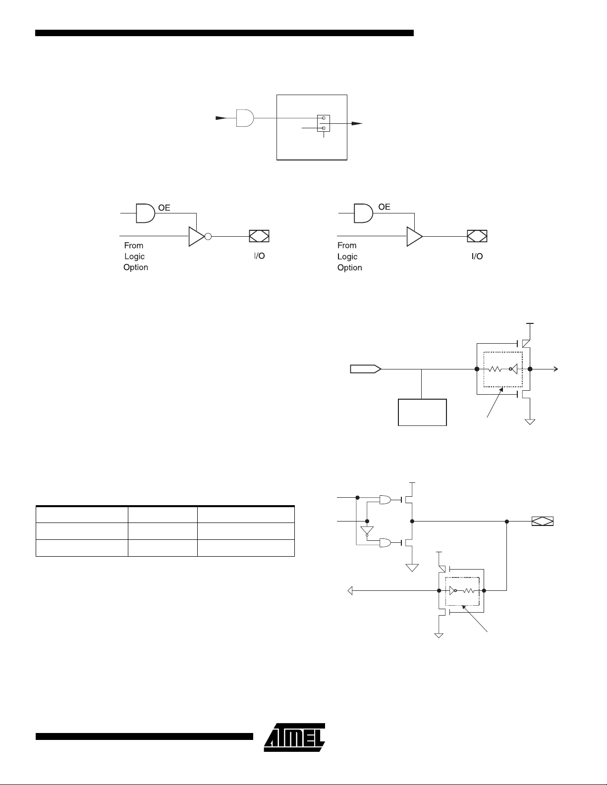
Clock Mux
Output Options
CLOCK
PRODUCT
TERM
CKi
CLK
PIN
ATF750LVC
CKMUX
TO
LOGIC
CELL
SELECT
Bus-friendly Pin-keeper Input and I/Os
All input and I/O pins on the ATF750LVC(L) have programmable “pin-keeper” circuits. If activated, when any pin is
driven high or low and then subsequently left floating, it will
stay at that previous high or low level.
This circuitry prevents unused input and I/O lines from
floating to intermediate voltage levels, which cause unnecessary power consumption and system noise. The keeper
circuits eliminate the need for external pull-up resistors and
eliminate their DC power consumption.
Enabling or disabling of the pin-keeper circuits is controlled
by the device type chosen in the logic compiler device
selection menu. Please refer to the software compiler table
for more details. Once the pin-keeper circuits are disabled,
normal termination procedures are required for unused
inputs and I/Os.
Table 1. Software Compiler Mode Selection
Synario Wincupl Pin-keeper Circuit
ATF750LVC V750C Disabled
ATF750LVC (PPK) V750CPPK Enabled
Input Diagram
INPUT
I/O Diagram
OE
DATA
ESD
PROTECTION
CIRCUIT
V
CC
V
CC
100K
PROGRAMMABLE
OPTION
V
CC
I/O
100K
PROGRAMMABLE
OPTION
3
Page 4
DC Characteristics
Symbol Parameter Condition Min Typ Max Units
I
LI
I
LO
I
CC
Input Load Current VIN = -0.1V to VCC + 1V 10 µA
Output Leakage
Current
Power Supply
Current, Standby
= -0.1V to VCC + 0.1V 10 µA
V
OUT
= Max,
V
CC
= Max,
V
IN
Outputs Open
C-15
Com. 65 90 mA
Ind. 70 100 mA
(1)(2)
I
OS
V
IL
V
IH
V
OL
V
OH
Output Short
Circuit Current
V
= 0.5V -120 mA
OUT
Input Low Voltage 3.0 ≤ VCC ≤ 3.6V -0.6 0.8 V
Input High Voltage 2.0 V
I
= 16 mA Com., Ind. 0.5 V
Output Low
Vol ta ge
Output High
Vol ta ge
VIN = VIH or VIL,
= Min
V
CC
VIN = VIH or VIL,
= Min
V
CC
OL
I
= 12 mA Mil. 0.5 V
OL
I
= 24 mA Com. 0.8 V
OL
= -2.0 mA 2.4 V
I
OH
+ 0.75 V
CC
Notes: 1. Not more than one output at a time should be shorted. Duration of short circuit test should not exceed 30 sec.
2. This test is performed at initial characterisation only.
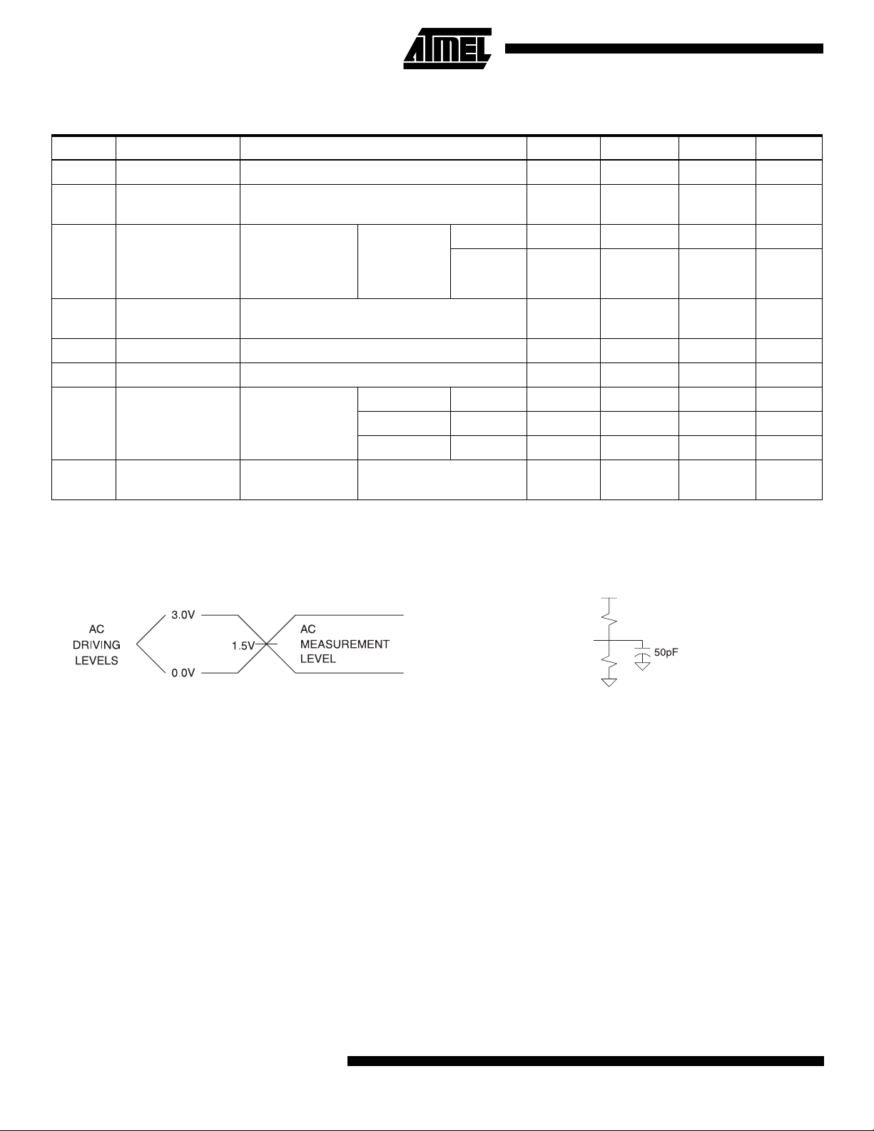
Input Test Waveforms and Measurement Levels
Output Test Load
VCC
316 Ω
348 Ω
tR, tF < 3 ns (10% to 90%)
4
ATF750LVC
Page 5
ATF750LVC
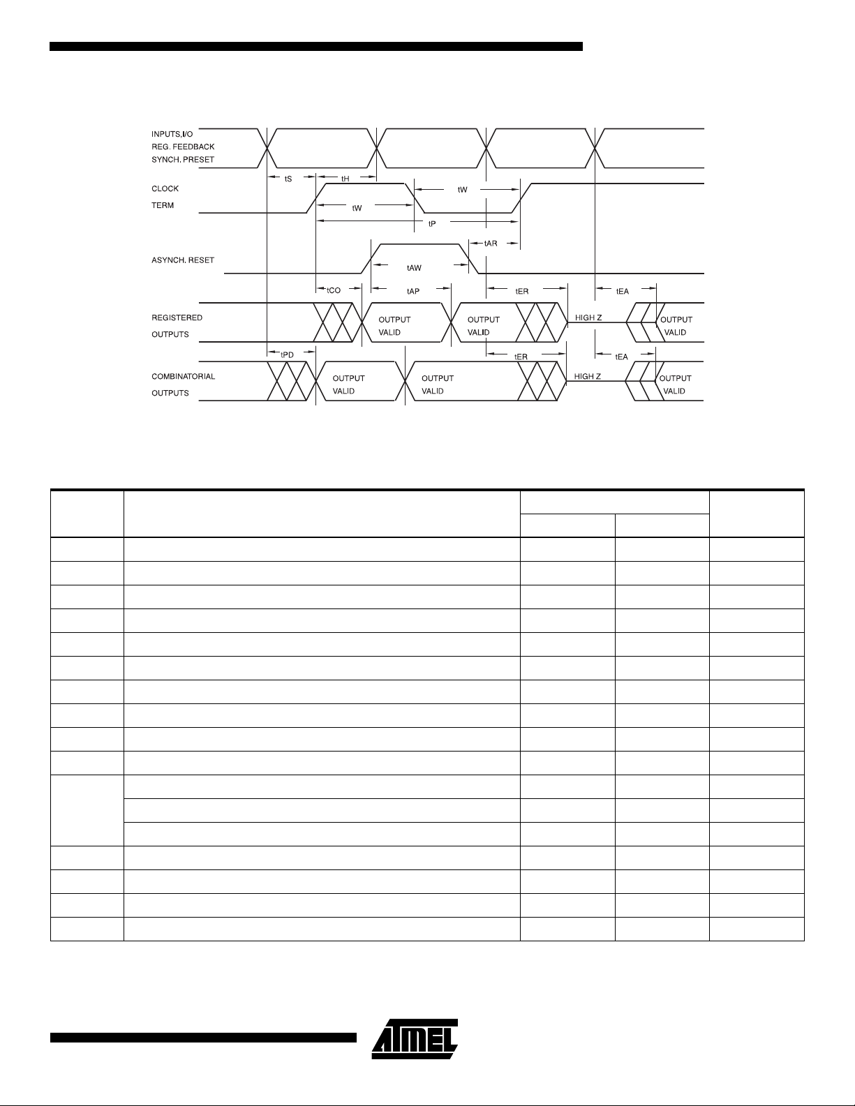
AC Waveforms, Product Term Clock
(1)
Note: 1. Timing measurement reference is 1.5V. Input AC driving levels are 0.0V and 3.0V, unless otherwise specified.
AC Characteristics, Product Term Clock
(1)
-15
Symbol Parameter
UnitsMin Max
t
PD
t
EA
t
ER
t
CO
t
CF
t
S
t
SF
t
H
t
P
t
W
Input or Feedback to Non-registered Output 15 ns
Input to Output Enable 15 ns
Input to Output Disable 15 ns
Clock to Output 5 12 ns
Clock to Feedback 5 9 ns
Input Setup Time 8 ns
Feedback Setup Time 7 ns
Hold Time 5 ns
Clock Period 14 ns
Clock Width 7 ns
External Feedback 1/(tS + tCO)50MHz
f
MAX
t
AW
t
AR
t
AP
t
SP
Internal Feedback 1/(tSF + tCF)62MHz
No Feedback 1/(t
) 71 MHz
P
Asynchronous Reset Width 15 ns
Asynchronous Reset Recovery Time 15 ns
Asynchronous Reset to Registered Output Reset 15 ns
Setup Time, Synchronous Preset 8 ns
Note: 1. See ordering information for valid part numbers.
5
Page 6
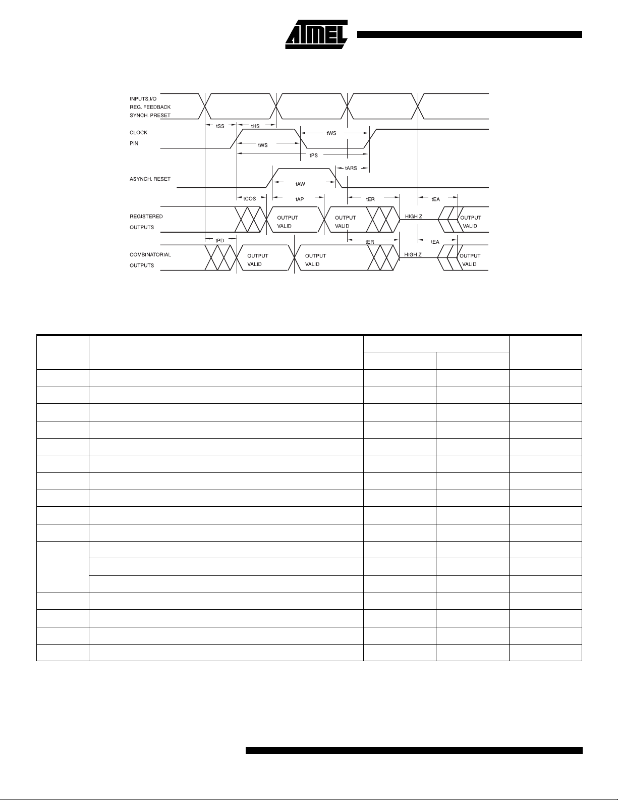
AC Waveforms, Input Pin Clock
(1)
Notes: 1. Timing measurement reference is 1.5V. Input AC driving levels are 0.0V and 3.0V, unless otherwise specified.
AC Characteristics, Input Pin Clock
-15
Symbol Parameter
UnitsMin Max
t
PD
t
EA
t
ER
t
COS
t
CFS
t
SS
t
SFS
t
HS
t
PS
t
WS
f
MAXS
t
AW
t
ARS
t
AP
t
SPS
Input or Feedback to Non-registered Output 15 ns
Input to Output Enable 15 ns
Input to Output Disable 15 ns
Clock to Output 0 10 ns
Clock to Feedback 0 5.5 ns
Input Setup Time 8 ns
Feedback Setup Time 7 ns
Hold Time 0 ns
Clock Period 12 ns
Clock Width 6 ns
External Feedback 1/(tSS + t
Internal Feedback 1/(t
No Feedback 1/(t
SFS
) 83 MHz
PS
)55MHz
COS
+ t
)80MHz
CFS
Asynchronous Reset Width 15 ns
Asynchronous Reset Recovery Time 15 ns
Asynchronous Reset to Registered Output Reset 15 ns
Setup Time, Synchronous Preset 11 ns
6
ATF750LVC
Page 7

Functional Logic Diagram ATF750LVC, Upper Half
ATF750LVC
7
Page 8

Functional Logic Diagram ATF750LVC, Lower Half
8
ATF750LVC
Page 9

ATF750LVC
Using the ATF750LVC’s Many Advanced Features
The ATF750LVC’s advanced flexibility packs more usable
gates into 24-pins than any other logic device. The
ATF750LVCs start with the popular 22V10 architecture,
and add several enhanced features:
• Selectable D- and T-type Registers
Each ATF750LVC flip-flop can be individually configured
as either D- or T-type. Using the T-type configuration, JK
and SR flip-flops are also easily created. These options
allow more efficient product term usage.
• Selectable Asynchronous Clocks
Each of the ATF750LVC’s flip-flops may be clocked by
its own clock product term or directly from Pin 1 (SMD
Lead 2). This removes the constraint that all registers
must use the same clock. Buried state machines,
counters and registers can all coexist in one device while
running on separate clocks. Individual flip-flop clock
source selection further allows mixing higher
performance pin clocking and flexible product term
clocking within one design.
• A Full Bank of Ten More Registers
The ATF750LVC provides two flip-flops per output logic
cell for a total of 20. Each register has its own sum term,
its own reset term and its own clock term.
• Independent I/O Pin and Feedback Paths
Each I/O pin on the ATF750LVC has a dedicated input
path. Each of the 20 registers has its own feedback
terms into the array as well. This feature, combined with
individual product terms for each I/O’s output enable,
facilitates true bi-directional I/O design.
Synchronous Preset and Asynchronous Reset
One synchronous preset line is provided for all 20 registers
in the ATF750LVC. The appropriate input signals to cause
the internal clocks to go to a high state must be received
during a synchronous preset. Appropriate setup and hold
times must be met, as shown in the switching waveform
diagram.
An individual asynchronous reset line is provided for each
of the 20 flip-flops. Both master and slave halves of the flipflops are reset when the input signals received force the
internal resets high.
Security Fuse Usage
A single fuse is provided to prevent unauthorized copying
of the ATF750LVC fuse patterns. Once the security fuse
is programmed, all fuses will appear programmed during
verify.
The security fuse should be programmed last, as its effect
is immediate.
9
Page 10

OUTPUT SOURCE CURRENT
VS SUPPLY VOLTAGE (V
0.0
-1.0
-2.0
-3.0
-4.0
(mA)
OH
I
-5.0
-6.0
-7.0
-8.0
3.00 3.25 3.30 3.50 3.60
SUPPLY VOLTAGE (V)
= 2.4V, TA = 25°C)
OH
OUTPUT SINK CURRENT
VS SUPPLY VOLTAGE (V
24.0
23.0
22.0
21.0
20.0
(mA)
OL
I
19.0
18.0
17.0
16.0
3.00 3.25 3.30 3.50 3.60
SUPPLY VOLTAGE (V)
= 0.5V, TA = 25°C)
OL
INPUT CURRENT VS
INPUT VOLTAGE (V
15.0
10.0
5.0
0.0
-5.0
INPUT CURRENT (µA)
-10.0
0.0 0.5 1.0 1.5 2.0 2.5 3.0 3.5 4.0
INPUT VOLTAGE (V)
= 3.3V, TA = 25°C)
CC
SUPPLY CURRENT
VS SUPPLY VOLTAGE (T
70.0
60.0
)
50.0
(mA
CC
I
40.0
= 25°C)
A
INPUT CLAMP CURRENT VS
INPUT VOLT AGE ( V
0.0
-10.0
-20.0
-30.0
-40.0
-50.0
INPUT CURRENT (mA)
-60.0
-70.0
0.0 -0.2 -0.4 -0.6 -0.8 -1.0
INPUT VOLTAGE (V)
= 3.3V, TA = 25°C)
CC
30.0
3.0 3.3 3.6
SUPPLY VOLTAGE (V)
10
ATF750LVC
Page 11

ATF750LVC
OUTPUT SOURCE CURRENT VS
OUTPUT VOLTAGE (V
0.0
-10.0
-20.0
-30.0
(mA)
-40.0
OH
I
-50.0
-60.0
-70.0
0.0 0.5 1.0 1.5 2.0 2.5 3.0 3.3
= 3.3V, TA = 25°C)
CC
(V)
V
OH
SUPPLY CURRENT VS INPUT FREQUENCY
(V
= 5.00V, TA = 25°C)
CC
80
40
(mA)
CC
I
OUTPUT SOURCE SINK CURRENT VS
OUTPUT VOLTAGE (V
80.0
70.0
60.0
50.0
40.0
(mA)
OL
I
30.0
20.0
10.0
0.0
0.0 0.5 1.0 1.5 2.0 2.5 3.0 3.3
= 3.3V, TA = 25°C)
CC
(V)
V
OL
0
0 5 10 15 20 50 75 100
FREQUENCY (MHz)
11
Page 12

ATF750LVC Ordering Information
Ext.
t
PD
(ns)
t
COS
(ns)
f
MAXS
(MHz) Ordering Code Package Operation Range
15 10 55 ATF750LVC-15JC
ATF750LVC-15PC
ATF750LVC-15SC
ATF750LVC-15XC
ATF750LVC-15JI
ATF750LVC-15PI
ATF750LVC-15SI
ATF750LVC-15X
Note: 1. Special order only; TSSOP package requires special thermal management.
(1)
(1)
I
28J
24P3
24S
24X
28J
24P3
24S
24X
Commercial
(0°C to 70°C)
(1)
Industrial
(-40°C to 85°C)
(1)
Using “C” Product for Industrial
Because the VCC conditions are the same for commercial and industrial for 3.3V products, and there is only 15°C difference
at the high end of the temperature range, there is very little risk in using “C” devices for industrial applications. Just de-rate
I
by 15%.
CC
Package Type
28J 28-Lead, Plastic J-leaded Chip Carrier (PLCC)
24P3 24-lead, 0.300’ Wide, Plastic Dual Inline Package (PDIP)
24S 24-lead, 0.300” Wide, Plastic Gull Wing Small Outline (SOIC)
24X* 24-lead, 0.173” Wide, Thin Shrink Small Outline (TSSOP)
12
ATF750LVC
Page 13

Packaging Information
ATF750LVC
28J, 28-lead, Plastic J-leaded Chip Carrier (PLCC)
Dimensions in Inches and (Millimeters)
JEDEC STANDARD MS-018 AB
.045(1.14) X 45°
.032(.813)
.026(.660)
.050(1.27) TYP
PIN NO. 1
IDENTIFY
.045(1.14) X 30° - 45°
.456(11.6)
SQ
.450(11.4)
.495(12.6)
.485(12.3)
.300(7.62) REF SQ
.022(.559) X 45° MAX (3X)
SQ
.012(.305)
.008(.203)
.430(10.9)
.390(9.91)
.021(.533)
.013(.330)
.043(1.09)
.020(.508)
.120(3.05)
.090(2.29)
.180(4.57)
.165(4.19)
SQ
24P3, 24-lead, 0.300" Wide, Plastic Dual Inline
Package (PDIP)
Dimensions in Inches and (Millimeters)
JEDEC STANDARD MS-001 AF
1.27(32.3)
SEATING
PLANE
.200(5.06)
MAX
.151(3.84)
.125(3.18)
.110(2.79)
.090(2.29)
.012(.305)
.008(.203)
1.25(31.7)
1.100(27.94) REF
PIN
1
.065(1.65)
.040(1.02)
.325(8.26)
.300(7.62)
0
REF
15
.400(10.2) MAX
.090(2.29)
.005(.127)
.070(1.78)
.020(.508)
.023(.584)
.014(.356)
.266(6.76)
.250(6.35)
MAX
MIN
24S, 24-lead, 0.300" Wide, Plastic Gull Wing Small
Outline (SOIC)
Dimensions in Inches and (Millimeters)
.020(.508)
.013(.330)
PIN 1 ID
.616(15.6)
.598(15.2)
0
REF
8
.299(7.60)
.291(7.39)
.050(1.27) BSC
.012(.305)
.003(.076)
.050(1.27)
.015(.381)
.420(10.7)
.393(9.98)
.105(2.67)
.092(2.34)
.013(.330)
.009(.229)
24X, 24-lead, 0.173" Wide, Thin Shrink Small Outline
(TSSOP)
Dimensions in Millimeters and (Inches)*
*Controlling dimension: millimeters
13
Page 14

Atmel Headquarters Atmel Operations
Corporate Headquarters
2325 Orchard Parkway
San Jose, CA 95131
TEL (408) 441-0311
FAX (408) 487-2600
Europe
Atmel U.K., Ltd.
Coliseum Business Centre
Riverside Way
Camberley, Surrey GU15 3YL
England
TEL (44) 1276-686-677
FAX (44) 1276-686-697
Asia
Atmel Asia, Ltd.
Room 1219
Chinachem Golden Plaza
77 Mody Road Tsimhatsui
East Kowloon
Hong Kong
TEL (852) 2721-9778
FAX (852) 2722-1369
Japan
Atmel Japan K.K.
9F, Tonetsu Shinkawa Bldg.
1-24-8 Shinkawa
Chuo-ku, Tokyo 104-0033
Japan
TEL (81) 3-3523-3551
FAX (81) 3-3523-7581
Atmel Colorado Springs
1150 E. Cheyenne Mtn. Blvd.
Colorado Springs, CO 80906
TEL (719) 576-3300
FAX (719) 540-1759
Atmel Rousset
Zone Industrielle
13106 Rousset Cedex
France
TEL (33) 4-4253-6000
FAX (33) 4-4253-6001
Atmel Smart Card ICs
Scottish Enterprise Technology Park
East Kilbride, Scotland G75
0QR
TEL (44) 1355-803-000
FAX (44) 1355-242-743
Atmel Grenoble
Avenue de Rochepleine
BP 123
38521 Saint-Egreve Cedex
France
TEL (33) 4-7658-3000
FAX (33) 4-7658-3480
Fax-on-Demand
North America:
1-(800) 292-8635
International:
1-(408) 441-0732
e-mail
literature@atmel.com
Web Site
http://www.atmel.com
BBS
1-(408) 436-4309
© Atmel Corporation 2001.
Atmel Corporation makes no warranty for the use of its products, other than those expressly contained in the Company’s standard warranty which is detailed in Atmel’s Terms and Conditions located on the Company’s web site. The Company assumes no responsibility for
any errors which may appear in this document, reserves the right to change devices or specifications detailed herein at any time without
notice, and does not make any commitment to update the information contained herein. No licenses to patents or other intellectual property of Atmel are granted by the Company in connection with the sale of Atmel products, expressly or by implication. Atmel’s products are
not authorized for use as critical components in life support devices or systems.
Marks bearing ® and/or ™ are registered trademarks and trademarks of Atmel Corporation.
Terms and product names in this document may be trademarks of others.
Printed on recycled paper.
1447D–03/01/xM
 Loading...