

Page 1
Features
• High-performance, High-density, Electrically-erasable Programmable Logic Device
• Fully Connected Logic Array with 416 Product Terms
• 10 ns Maximum Pin-to-pin Delay for 5V Operation
• Low-power Edge-sensing “L” Option with <1 mA Standby Current
• 24 Flexible Output Macrocells
– 48 Flip-flops – Two per Macrocell
–72 Sum Terms
– All Flip-flops, I/O Pins Feed in Independently
• D- or T-type Flip-flops
• Product Term or Direct Input Pin Clocking
• Registered or Combinatorial Internal Feedback
• Backward Compatible with ATV2500B/BQL and ATV2500H/L Software
• Advanced Electrically-erasable Technology
– Reprogrammable
– 100% Tested
• 44-lead Surface Mount Package
ATF2500C
CPLD Family
Datasheet
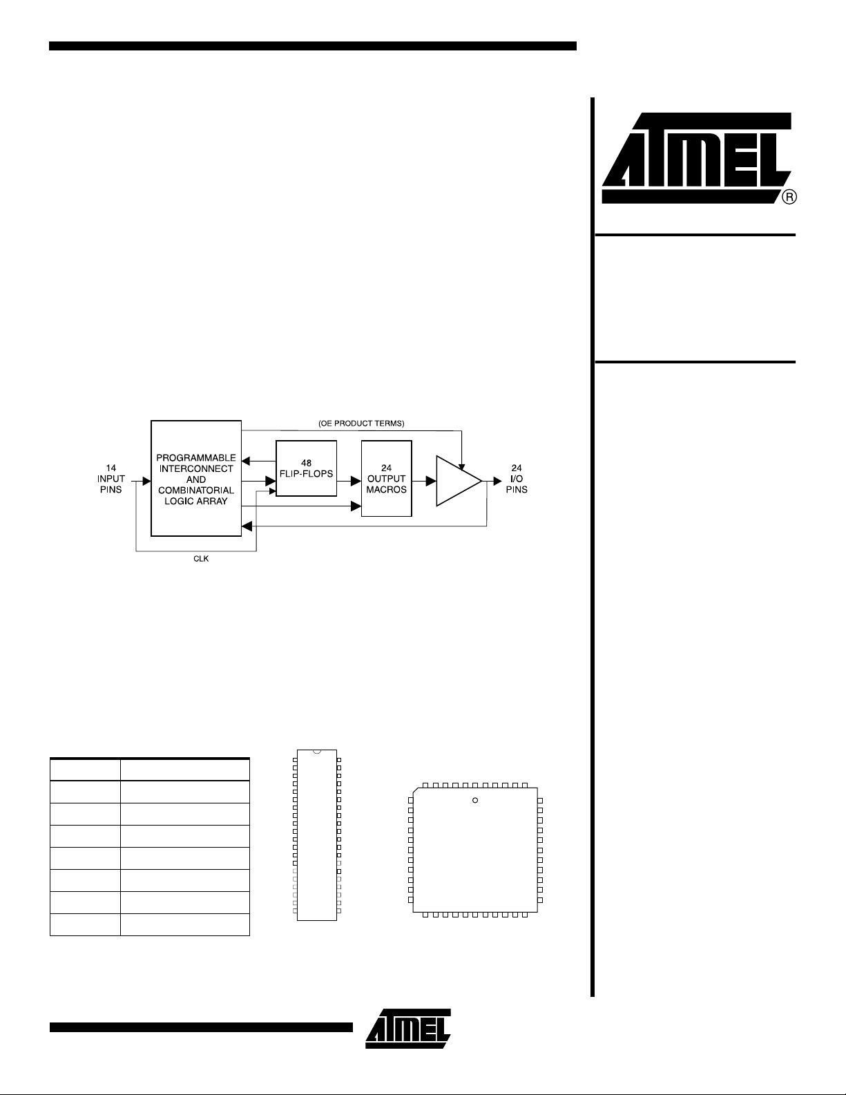
Block Diagram
Description
The ATF2500C is the highest-density PLD available in a 44-pin package. With its fully
connected logic array and flexible macrocell structure, high gate utilization is easily
obtainable. The ATF2500C is a high-performance CMOS (electrically-erasable) programmable logic device (PLD) that utilizes Atmel’s proven electrically-erasable
technology.
Pin Configurations
Pin Name Function
IN Logic Inputs
CLK/IN Pin Clock and Input
I/O Bi-directional Buffers
I/O 0,2,4... “Even” I/O Buffers
I/O 1,3,5... “Odd” I/O Buffers
GND Ground
VCC +5V Supply
VCC
I/O17
I/O16
I/O15
I/O14
I/O13
I/O12
DIP
1
IN
IN
IN
I/O0
I/O1
I/O2
I/O3
I/O4
I/O5
IN
IN
IN
IN
40
2
3
4
5
6
7
8
9
10
11
12
13
14
15
16
17
18
19
20
IN
39
IN
38
IN
37
IN
36
I/O6
35
I/O7
34
I/O8
33
I/O9
32
I/O10
31
I/O11
30
GND
29
I/O23
28
I/O22
27
I/O21
26
I/O20
25
I/O19
24
I/O18
23
IN
22
IN
21
IN
PLCC/LCC/JLCC
I/O1
I/O0
65432
7
I/O2
8
I/O3
9
I/O4
10
I/O5
11
VCC
12
VCC
13
I/O17
14
I/O16
15
I/O15
16
I/O14
17
I/O13
1819202122232425262728
INININININININ
I/O12
GNDININ
CLK/INININININ
1
4443424140
IN
I/O18
I/O6
39
38
37
36
35
34
33
32
31
30
29
I/O19
I/O7
I/O8
I/O9
I/O10
I/O11
GND
GND
I/O23
I/O22
I/O21
I/O20
ATF2500C
ATF2500CL
ATF2500CQ
ATF2500CQL
Preliminary
Note: For ATF2500CQ and ATF2500CQL
(PLCC/LCC/JLCC packages) pin 4 and pin 26
GND connections are not required.
Rev. 0777G–12/01
1
Page 2

The ATF2500C is organized around a single universal array. All pins and feedback terms are
always available to every macrocell. Each of the 38 logic pins are array inputs, as are the outputs of each flip-flop.
In the ATF2500C, four product terms are input to each sum term. Furthermore, each macrocell’s three sum terms can be combined to provide up to 12 product terms per sum term with
no performance penalty. Each flip-flop is individually selectable to be either D- or T-type, providing further logic compaction. Also, 24 of the flip-flops may be bypassed to provide internal
combinatorial feedback to the logic array.
Product terms provide individual clocks and asynchronous resets for each flip-flop. The flipflops may also be individually configured to have direct input pin clocking. Each output has its
own enable product term. Eight synchronous preset product terms serve local groups of either
four or eight flip-flops. Register preload functions are provided to simplify testing. All registers
automatically reset upon power-up.
The Atmel-unique “L” low-power feature is an edge-sensing option that is now field programmable for the ATF2500C family. The “L” feature utilizes Atmel-patented Input Transition
Detection (ITD) circuitry and is activated by selecting the “L” option from the program menu.
Using the ATF2500C Family’s Many Advanced Features
The ATF2500Cs advanced flexibility packs more usable gates into 44 leads than other PLDs.
Some of the ATF2500Cs key features are:
• Fully Connected Logic Array – Each array input is always available to every product
term. This makes logic placement a breeze.
• Selectable D- and T-Type Registers – Each ATF2500C flip-flop can be individually
configured as either D- or T-type. Using the T-type configuration, JK and SR flip-flops are
also easily created. These options allow more efficient product term usage.
• Buried Combinatorial Feedback – Each macrocell’s Q2 register may be bypassed to
feed its input (D/T2) directly back to the logic array. This provides further logic expansion
capability without using precious pin resources.
• Selectable Synchronous/Asynchronous Clocking – Each of the ATF2500Cs flip-flops
has a dedicated clock product term. This removes the constraint that all registers use the
same clock. Buried state machines, counters and registers can all coexist in one device
while running on separate clocks. Individual flip-flop clock source selection further allows
mixing higher performance pin clocking and flexible product term clocking within one
design.
• A Total of 48 Registers – The ATF2500C provides two flip-flops per macrocell – a total of
48. Each register has its own clock and reset terms, as well as its own sum term.
• Independent I/O Pin and Feedback Paths – Each I/O pin on the ATF2500C has a
dedicated input path. Each of the 48 registers has its own feedback term into the array as
well. These features, combined with individual product terms for each I/O’s output enable,
facilitate true bi-directional I/O design.
• Combinable Sum Terms – Each output macrocell’s three sum terms may be combined
into a single term. This provides a fan in of up to 12 product terms per sum term with no
speed penalty.
2
ATF2500C Family
0777G–12/01
Page 3
ATF2500C Family
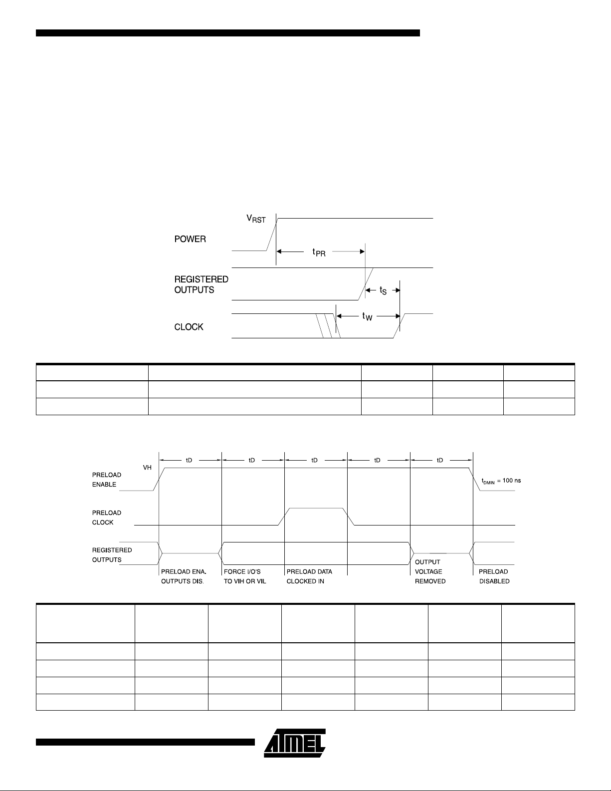
Power-up Reset The registers in the ATF2500Cs are designed to reset during power-up. At a point delayed
slightly from V
crossing V
CC
depend on the polarity of the output buffer.
, all registers will be reset to the low state. The output state will
RST
This feature is critical for state as nature of reset and the uncertainty of how V
actually rises
CC
in the system, the following conditions are required:
1. The V
rise must be monotonic,
CC
2. After reset occurs, all input and feedback setup times must be met before driving the
clock pin or terms high, and
3. The clock pin, and any signals from which clock terms are derived, must remain stable
during t
Parameter Description Typ Max Units
t
PR
V
RST
Power-up Reset Time 600 1000 ns
Power-up Reset Voltage 3.8 4.5 V
PR
.
Level Forced on
Odd I/O Pin during
PRELOAD Cycle
V
IH/VIL
V
IH/VIL
V
IH/VIL
VIH/V
IL
0777G–12/01
Q Select Pin
State
Even/Odd
Select
Even Q1 State
after Cycle
Even Q2 State
after Cycle
Odd Q1 State
after Cycle
Odd Q2 State
after Cycle
Low Low High/Low X X X
High Low X High/Low X X
Low High X X High/Low X
High High X X X High/Low
3
Page 4

Preload and Observability of Registered Outputs
The ATF2500Cs registers are provided with circuitry to allow loading of each register asynchronously with either a high or a low. This feature will simplify testing since any state can be
forced into the registers to control test sequencing. A V
appropriate register high; a V
tion bit settings.
The PRELOAD state is entered by placing an 10.25V to 10.75V signal on SMP lead 42. When
the preload clock SMP lead 23 is pulsed high, the data on the I/O pins is placed into the 12
registers chosen by the Q select and even/odd select pins.
Register 2 observability mode is entered by placing an 10.25V to 10.75V signal on pin/lead 2.
In this mode, the contents of the buried register bank will appear on the associated outputs
when the OE control signals are active.
will force it low, independent of the polarity or other configura-
IL
level on the odd I/O pins will force the
IH
Programming Software Support
Security Fuse Usage
Input and I/O Pull-ups
All family members of the ATF2500C can be designed with Atmel-Synario™ and Atmel-Win-
™
CUPL
Additionally, the ATF2500C may be programmed to perform the ATV2500H/Ls functional subset (no T-type flip-flops, pin clocking or D/T2 feedback) using the ATV2500H/L JEDEC file. In
this case, the ATF2500C becomes a direct replacement or speed upgrade for the
ATV2500H/L. The ATF2500CQ/CQL are direct replacements for the ATV2500BQ/BQL and
the AT2500H/L, including the lack of extra grounds on P4 and P26.
A single fuse is provided to prevent unauthorized copying of ATF2500C fuse patterns. Once
programmed, the outputs will read programmed during verify.
The security fuse should be programmed last, as its effect is immediate.
The security fuse also inhibits Preload and Q2 observability.
All ATF2500C family members have programmable internal input and I/O pinkeeper circuits.
The default condition, including when using the AT2500CQ/CQL family to replace the
AT2500BQ/BQL or AT2500H/L, is that the pinkeepers are not activated.
When pinkeepers are active, inputs or I/Os not being driven externally will maintain their last
driven state. This ensures that all logic array inputs and device outputs are known states.
Pinkeepers are relatively weak active circuits that can be easily overridden by TTL-compatible
drivers (see input and I/O diagrams below).
. ProChip™ designer support will be available Q102.
4
ATF2500C Family
0777G–12/01
Page 5
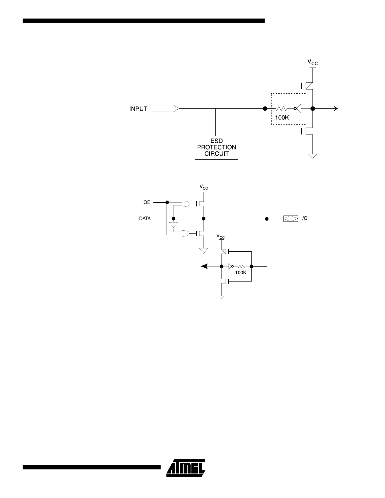
Input Diagram
I/O Diagram
ATF2500C Family
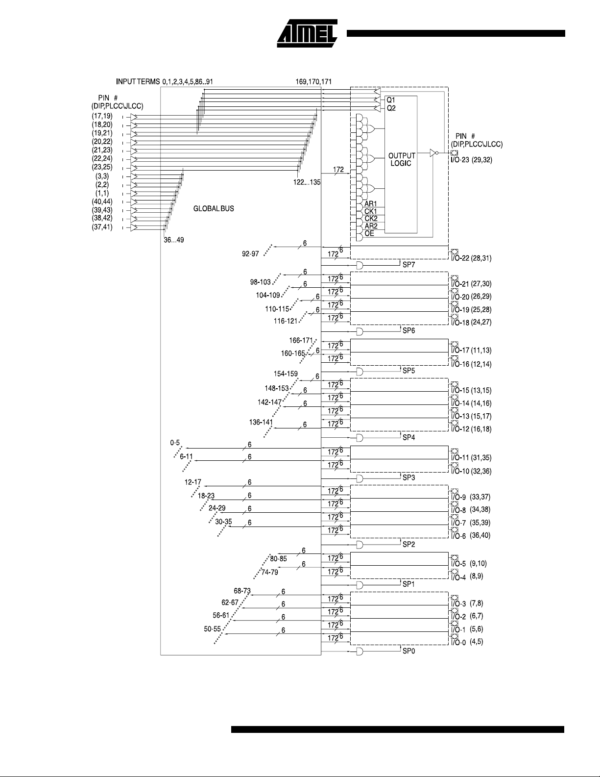
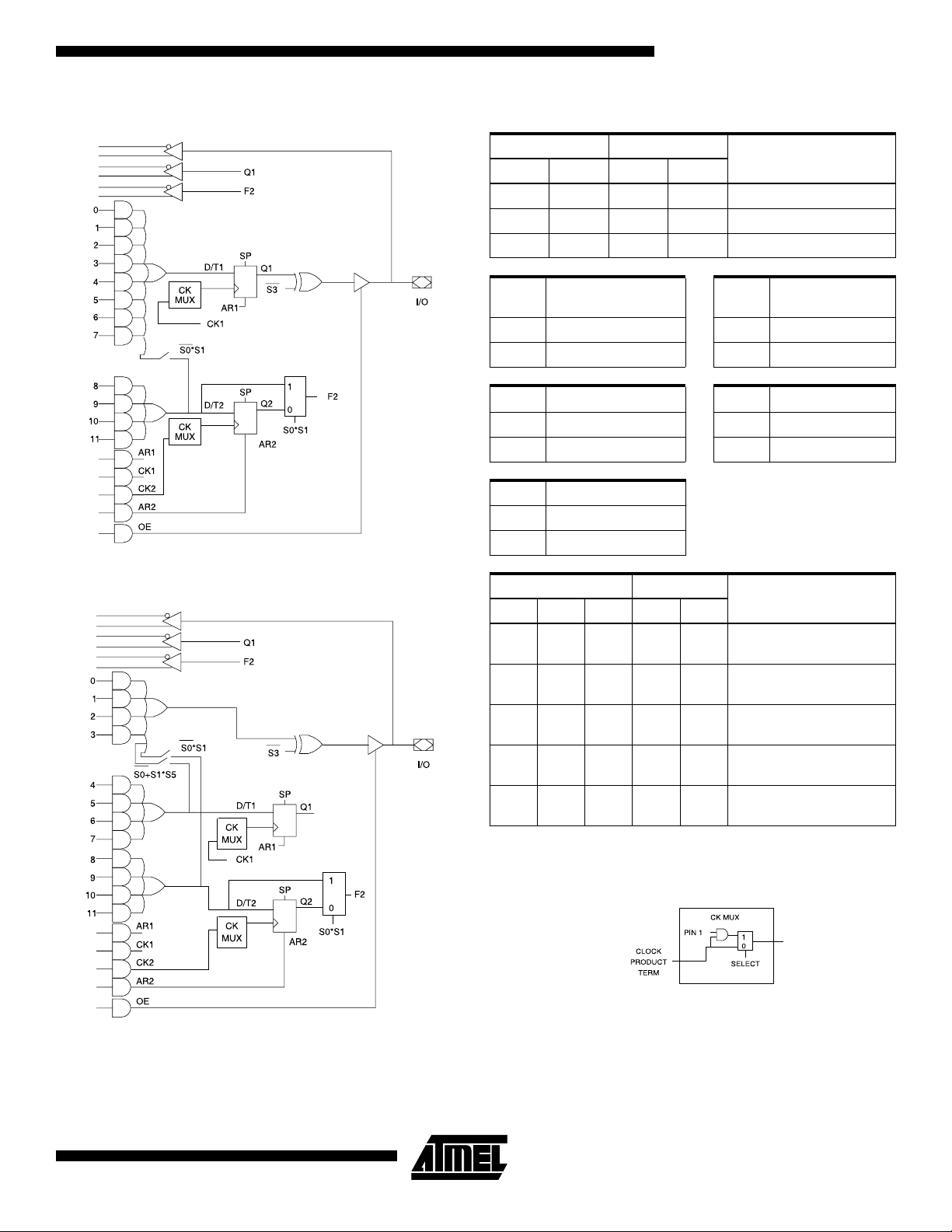
Functional Logic Diagram Description
INPUT
The ATF2500C functional logic diagram describes the interconnections between the input,
feedback pins and logic cells. All interconnections are routed through the single global bus.
The ATF2500Cs are straightforward and uniform PLDs. The 24 macrocells are numbered 0
through 23. Each macrocell contains 17 AND gates. All AND gates have 172 inputs. The five
lower product terms provide AR1, CK1, CK2, AR2, and OE. These are: one asynchronous
reset and clock per flip-flop, and an output enable. The top 12 product terms are grouped into
three sum terms, which are used as shown in the macrocell diagrams.
Eight synchronous preset terms are distributed in a 2/4 pattern. The first four macrocells share
Preset 0, the next two share Preset 1, and so on, ending with the last two macrocells sharing
Preset 7.
The 14 dedicated inputs and their complements use the numbered positions in the global bus
as shown. Each macrocell provides six inputs to the global bus: (left to right) feedback F2
true and false, flip-flop Q1 true and false, and the pin true and false. The positions occupied by
these signals in the global bus are the six numbers in the bus diagram next to each macrocell.
Note: 1. Either the flip-flop input (D/T2) or output (Q2) may be fed back in the ATF2500Cs.
(1)
0777G–12/01
5
Page 6
Functional Logic Diagram ATV2500C
Notes: 1. Pin 4 and Pin 26 are “ground” connections and are not required for PLCC, LCC and JLCC versions of ATF2500CQ or
ATF2500CQL, making them compatible with ATV2500H and ATV2500L as well as ATV2500BQ and ATV2500BQL pinouts.
2. For DIP package, VCC = P10 and GND = P30. For, PLCC, LCC and JLCC packages, VCC = P11 and P12, GND1 = P33 and
P34, and GND2 = P4, P26 (See Note 1, above).
6
ATF2500C Family
0777G–12/01
Page 7
ATF2500C Family
Output Logic, Registered
(1)
S2 = 0 Terms in
Output ConfigurationS1 S0 D/T1 D/T2
0084Registered (Q1); Q2 FB
(1)
10124
1184Registered (Q1); D/T2 FB
Output
S3
Configuration S6 Q1 CLOCK
0 Active Low 0 CK1
1 Active High 1 CK1 • PIN1
S4 Register 1 Type S7
0D 0CK2
1T 1CK2 • PIN1
S5 Register 2 Type
0D
1T
Registered (Q1); Q2 FB
Q2 CLOCK
Output Logic, Combinatiorial
(1)
S2 = 1 Terms in
Output ConfigurationS5 S1 S0 D/T1 D/T2
X004
X0144
X104
1114
01144
(1)
(1)
(1)
Combinatorial (8 Terms);
4
Q2 FB
Combinatorial (4 Terms);
Q2 FB
Combinatorial (12 Terms);
(1)
4
Q2 FB
Combinatorial (8 Terms);
4
D/T2 FB
Combinatorial (4 Terms);
D/T2 FB
Note: 1. These four terms are shared with D/T1.
Clock Option
Note: 1. These diagrams show equivalent logic functions, not
necessarily the actual circuit implementation.
0777G–12/01
7
Page 8
Absolute Maximum Ratings*
Temperature Under Bias................................ -55°C to +125°C
Storage Temperature ..................................... -65°C to +150°C
Junction Temperature .............................................150°C Max
Voltage on Any Pin with
Respect to Ground .........................................-2.0V to +7.0V
Voltage on Input Pins
with Respect to Ground
During Programming.....................................-2.0V to +14.0V
Programming Voltage with
Respect to Ground .......................................-2.0V to +14.0V
DC and AC Operating Conditions
Commercial Industrial Military
*NOTICE: Stresses beyond those listed under “Absolute
Maximum Ratings” may cause permanent damage to the device. This is a stress rating only and
functional operation of the device at these or any
other conditions beyond those indicated in the
operational sections of this specification is not
(1)
Note: 1. Minimum voltage is -0.6V DC which may under-
(1)
(1)
implied. Exposure to absolute maximum rating
conditions for extended periods may affect device
reliability.
shoot to -2.0V for pulses of less than 20 ns.
Maximum output pin voltage is V
which may overshoot to +7.0V for pulses of less
than 20 ns.
+ 0.75V DC
CC
Operating Temperature
V
Power Supply 5V ± 5% 5V ± 10% 5V ± 10%
CC
0°C - 70°C
(Ambient)
-40°C - 85°C
(Ambient)
Pin Capacitance
f = 1 MHz, T = 25°C
C
IN
C
OUT
Note: 1. Typical values for nominal supply voltage. This parameter is only sampled and is not 100% tested.
(1)
Typ Max Units Conditions
46pFV
812pFV
= 0V
IN
OUT
= 0V
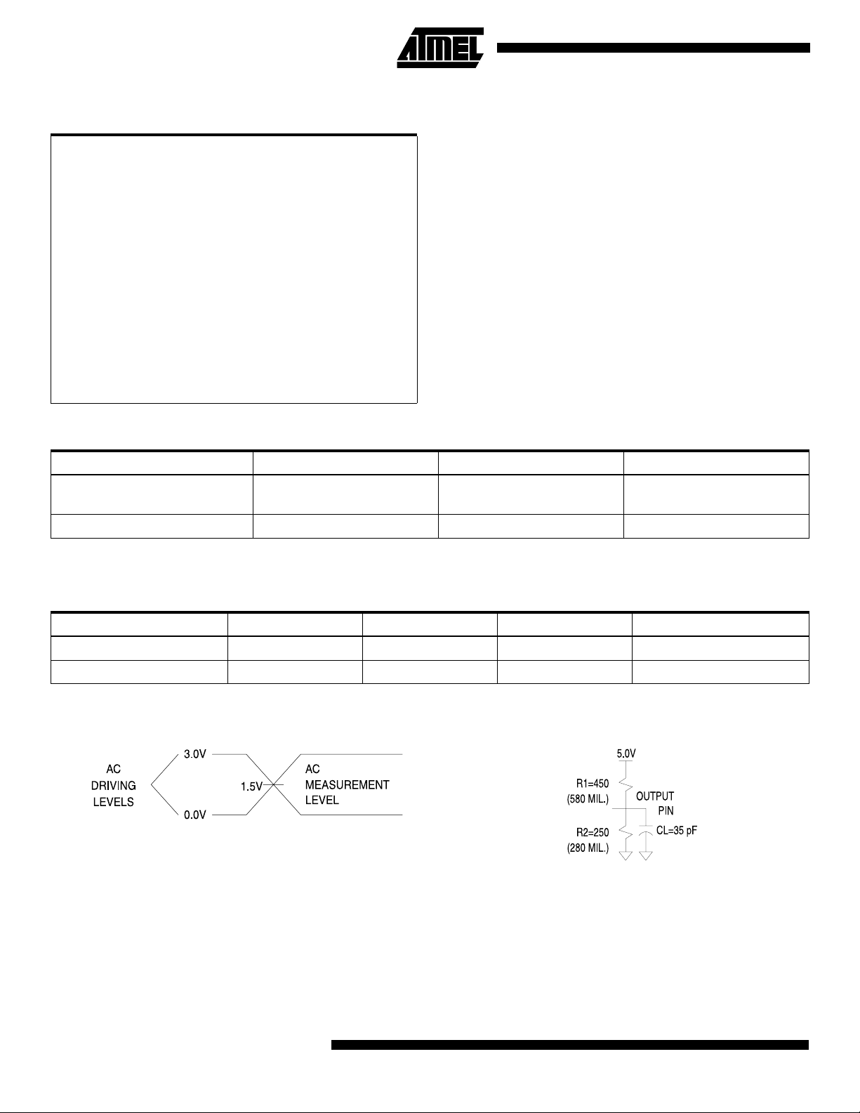
Test Waveforms and Measurement Levels Output Test Load
-55°C - 125°C
(Case)
8
ATF2500C Family
0777G–12/01
Page 9
ATF2500C Family
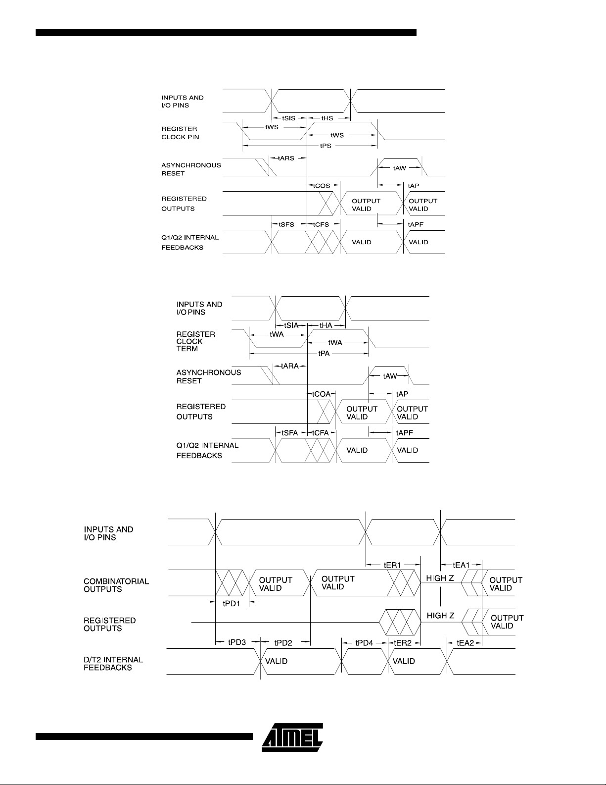
AC Waveforms
AC Waveforms
(1)
Input Pin Clock
(1)
Product Term Clock
(1)
AC Waveforms
Note: 1. Timing measurement reference is 1.5V. Input AC driving levels are 0.0V and 3.0V, unless otherwise specified.
0777G–12/01
Combinatorial Outputs and Feedback
9
Page 10
ATF2500C DC Characteristics
Symbol Parameter Condition Min Typ Max Units
I
IL
I
LO
I
CC
Input Load Current VIN = -0.1V to VCC + 1V 10 µA
Output Leakage
Current
Power Supply
Current Standby
= -0.1V to VCC + 0.1V
V
OUT
= MAX,
V
CC
V
= GND or
IN
f = 0 MHz,
V
CC
ATF2500C
Outputs Open
I
OS
V
IL
V
IH
V
OL
V
OH
Output Short
Circuit Current
Input Low Voltage MIN ≤ VCC ≤ MAX -0.6 0.8 V
Input High Voltage 2.0 VCC + 0.75 V
Output Low
Volt age
Output High
Volt age
= 0.5V
V
OUT
VIN = VIH or VIL,
V
= 4.5V
CC
= MIN
V
CC
I
= 8 mA Com., Ind. 0.5 V
OL
IOL = 6 mA Mil. 0.5 V
I
= -100 µA VCC - 0.3 V
OH
I
= -4.0 mA 2.4
OH
Note: 1. See ICC versus frequency characterization curves.
ATF2500C AC Characteristics
Symbol Parameter
Com.
Ind., Mil.
10 µA
110 190 mA
110 210 mA
-120 mA
-10 -15
UnitsMinMaxMinMax
t
t
t
t
t
t
t
t
t
t
t
PD1
PD2
PD3
PD4
EA1
ER1
EA2
ER2
AW
AP
APF
Input to Non-registered Output 10 15 ns
Feedback to Non-registered Output 10 15 ns
Input to Non-registered Feedback 6 11 ns
Feedback to Non-registered Feedback 6 11 ns
Input to Output Enable 10 15 ns
Input to Output Disable 10 15 ns
Feedback to Output Enable 10 15 ns
Feedback to Output Disable 10 15 ns
Asynchronous Reset Width 4 8 ns
Asynchronous Reset to Registered Output 13 18 ns
Asynchronous Reset to Registered Feedback 10 15 ns
10
ATF2500C
0777G–12/01
Page 11
ATF2500C Register AC Characteristics, Input Pin Clock
-10 -15
Symbol Parameter
t
COS
t
CFS
t
SIS
t
SFS
t
HS
t
WS
t
PS
Clock to Output 5.5 10 ns
Clock to Feedback 0 2 0 5 ns
Input Setup Time 2 9 ns
Feedback Setup Time 2 9 ns
Hold Time 0 0 ns
Clock Width 3 6 ns
Clock Period 8 12 ns
External Feedback 1/(t
F
MAXS
Internal Feedback 1/(t
No Feedback 1/(tPS)11083MHz
SIS
SFS
+ t
)7552MHz
COS
+ t
)10071MHz
CFS
Min Max Min Max
ATF2500C
Units
t
ARS
Asynchronous Reset/Preset Recovery Time 5 12 ns
ATF2500C Register AC Characteristics, Product Term Clock
-10 -15
Symbol Parameter
t
COA
t
CFA
t
SIA
t
SFA
t
HA
t
WA
t
PA
F
t
ARA
MAXA
Clock to Output 10 15 ns
Clock to Feedback 2 5 5 12 ns
Input Setup Time 2 5 ns
Feedback Setup Time 2 5 ns
Hold Time 1 5 ns
Clock Width 3 7.5 ns
Clock Period 9 15 ns
External Feedback 1/(t
Internal Feedback 1/(t
No Feedback 1/(t
PS
+ t
SIA
SFA
)75.550MHz
COA
+ t
)10058MHz
CFA
)10066MHz
Asynchronous Reset/Preset Recovery Time 2 8 ns
UnitsMin Max Min Max
0777G–12/01
11
Page 12
STAND-BY ICC VS.
4.5
SUPPLY VOLTAGE (T
4.0
3.5
3.0
2.5
(µA)
2.0
CC
I
1.5
1.0
0.5
0.0
4.5 4.8 5.0 5.3 5.5
TBD
SUPPLY VOLTAGE (V)
= 25°C)
A
NORMALIZED ICC VS. TE MP
1.4
1.2
1.0
0.8
0.6
NORMALIZED Icc
0.4
-40.0 0.0 25.0 75.0
TBD
TEMPERATURE (C)
SUPPLY CURRENT VS.
140.000
120.000
100.000
80.000
(mA)
CC
60.000
I
40.000
20.000
INPUT FREQUENCY (V
0.000
0.0 0.5 2. 5 5.0 7. 5 10. 0 25.0 37.5 50. 0
FREQUENCY (MHz)
= 5.0V, TA = 25°C)
CC
TBD
OUTPUT SOURCE CURRENT VS.
0
SUPPLY VOLTAGE (V
-10
-20
(mA)
-30
OH
I
-40
TBD
-50
4.0 4.5 5.0 5.5 6.0
SUPPLY VOLTAGE (V)
= 2.4V)
OH
SUPPLY CURRENT VS.
1.000
INPUT FREQUENCY (V
0.800
0.600
(mA)
0.400
CC
I
0.200
0.000
0.0 0.5 2.5 5.0 7.5 10.0 25.0 37.5 50.0
FREQUENCY (MHz)
= 5.0V, TA = 25°C)
CC
TBD
OUTPUT SOURCE CURRENT VS.
OUTP UT VOL TAGE (V
0.0
-10.0
-20.0
-30.0
-40.0
(mA)
-50.0
OH
I
-60.0
-70.0
-80.0
-90.0
0.00 0.50 1. 00 1.50 2. 00 2.50 3.00 3. 50 4.00 4. 50 5 .00
= 5.0V, TA = 25°C)
CC
TBD
V
(V)
OH
OUTPUT SINK CURRENT VS.
1
1
1
0
Iol (mA)
0
0
4.0 4.5 5.0 5. 5 6.0
12
SUPPLY VOLTAGE (V
TBD
SUPPLY VOLTAGE (V)
ATF2500C
= 0.5V)
OL
OUTPUT SINK CURRENT VS.
140.0
120.0
100.0
80.0
(mA)
60.0
OL
I
40.0
20.0
0.0
0.0 0.5 1.0 1.5 2.0 2.5 3.0 3.5 4.0 4.5 5.0
OUTPUT VOLTAGE (V
SUPPLY VOLTAGE (V)
= 5.0V, TA = 25°C)
CC
TBD
0777G–12/01
Page 13

ATF2500C
INPUT CLAMP CURRENT VS.
INPUT VOLTAGE (V
0
-20
-40
-60
INPUT
-80
-100
CURRENT (mA)
-120
0.0 -0.2 -0.4 -0.6 -0.8 -1.0
1.2
PD
1.1
1.0
0.9
NORMALIZED T
0.8
4.5 4.8 5.0 5.3 5.5
INPUT VOLTAGE (V )
NORMALIZED TPD VS. VCC
SUPPLY VOLTAGE (V)
= 5.0V, TA = 35°C)
CC
TBD
TBD
INPUT CURRENT VS.
INPUT VOLTAGE (V
1
1
1
(uA)
0
0
INPUT CURRENT
0
0.01.02.03.04.05.06.0
1.1
PD
1.0
0.9
NORMALIZED T
0.8
-40.0 0.0 25.0 75.0
INPUT VOLTAGE (V)
NORMALIZED TPD VS . TEMP
TEMPERATURE (C)
= 5.0V, TA = 25°C)
CC
TBD
TBD
1.3
CO
1.2
1.1
1.0
0.9
NORMALIZED T
0.8
4.5 4.8 5.0 5.3 5.5
1.2
PD
1.1
1.0
0.9
NORMALIZED T
0.8
4.5 4.8 5.0 5.3 5.5
NORMALIZED TCO VS. VCC
TBD
SUPPLY VOLTAGE (V)
NORMALIZED TPD VS. VCC
TBD
SUPPLY VOLTAGE (V)
1.1
CO
1.0
TBD
0.9
NORMALIZED T
0.8
-40.0 0.0 25.0 75.0
TEM PERAT URE (V )
NORMALIZED TSU VS. TEMP
1.2
CO
1.1
NORMALIZED TCO VS. TEMP
1.0
0.9
NORMALIZED T
0.8
-40.0 0.0 25.0 75.0
TBD
TEMP ERATURE (C)
0777G–12/01
13
Page 14

DELTA TPD VS.
8
6
(ns)
4
PD
2
DELTA T
0
-2
0 50 100 150 200 250 300
OUTPUT LOADING
TBD
OUTPUT LOADING (PF)
DELTA TCO VS.
1.00
0.90
0.80
0.70
(ns)
0.60
CO
0.50
0.40
0.30
0.20
DELTA T
0.10
0.00
50 100 150 200 250 300
OUTPUT LOADING
TBD
NUMBER OF OUTPUTS LOADING
DELTA TPD VS . # OF OU TPU T S WIT CHIN G
0.0
-0.1
(ns)
PD
-0.2
-0.3
DELTA T
-0.4
-0.5
1.02.03.04.05.06.07.08.09.010.0
NUMBER OF OUTPUTS SWITCHING
TBD
DELTA TCO VS. # OF OUTPUT SWITCHING
0.0
-0.1
(ns)
PD
-0.2
-0.3
DELTA T
-0.4
-0.5
1.0 2. 0 3.0 4. 0 5. 0 6.0 7. 0 8.0 9.0 10.0
NUMBER OF OUTPUTS SWITCHING
TBD
14
ATF2500C
0777G–12/01
Page 15

ATF2500CL
ATF2500CL DC Characteristics
Symbol Parameter Condition Min Typ Max Units
I
IL
I
LO
I
CC
Input Load Current VIN = -0.1V to VCC + 1V 10 µA
Output Leakage
Current
Power Su pply
Current Standby
= -0.1V to VCC + 0.1V
V
OUT
= MAX,
V
CC
V
= GND or
IN
f = 0 MHz,
V
CC
ATF2500CL
Outputs Open
I
OS
V
IL
V
IH
V
OL
V
OH
Output Short
Circuit Current
Input Low Voltage MIN ≤ VCC ≤ MAX -0.6 0.8 V
Input High Voltage 2.0 VCC + 0.75 V
Output Low Voltage
Output High
Vol tage
= 0.5V
V
OUT
VIN = VIH or VIL,
V
= 4.5V
CC
= MIN
V
CC
I
= 8 mA Com., Ind. 0.5 V
OL
IOL = 6 mA Mil. 0.5 V
I
= -100 µA VCC - 0.3 V
OH
I
= -4.0 mA 2.4
OH
Note: 1. See ICC versus frequency characterization curves.
ATF2500CL AC Characteristics
Symbol Parameter
Com.
Ind., Mil.
10 µA
25 mA
210 mA
-120 mA
-20
UnitsMin Max
t
t
t
t
t
t
t
t
t
t
t
PD1
PD2
PD3
PD4
EA1
ER1
EA2
ER2
AW
AP
APF
Input to Non-registered Output 20 ns
Feedback to Non-registered Output 20 ns
Input to Non-registered Feedback 15 ns
Feedback to Non-registered Feedback 15 ns
Input to Output Enable 20 ns
Input to Output Disable 20 ns
Feedback to Output Enable 20 ns
Feedback to Output Disable 20 ns
Asynchronous Reset Width 12 ns
Asynchronous Reset to Registered Output 22 ns
Asynchronous Reset to Registered Feedback 19 ns
0777G–12/01
15
Page 16

ATF2500CL Register AC Characteristics, Input Pin Clock
Symbol Parameter
t
COS
t
CFS
t
SIS
t
SFS
t
HS
t
WS
t
PS
Clock to Output 11 ns
Clock to Feedback 0 6 ns
Input Setup Time 14 ns
Feedback Setup Time 14 ns
Hold Time 0 ns
Clock Width 7 ns
Clock Period 14 ns
External Feedback 1/(t
F
MAXS
Internal Feedback 1/(t
No Feedback 1/(tPS) 71 MHz
SIS
SFS
+ t
)40MHz
COS
+ t
)50MHz
CFS
Min Max
-20
Units
t
ARS
Asynchronous Reset/Preset Recovery Time 15 ns
ATF2500CL Register AC Characteristics, Product Term Clock
Symbol Parameter
t
COA
t
CFA
t
SIA
t
SFA
t
HA
t
WA
t
PA
Clock to Output 20 ns
Clock to Feedback 10 16 ns
Input Setup Time 10 ns
Feedback Setup Time 8 ns
Hold Time 10 ns
Clock Width 11 ns
Clock Period 22 ns
External Feedback 1/(t
F
MAXA
Internal Feedback 1/(t
No Feedback 1/(t
t
ARA
Asynchronous Reset/Preset Recovery Time 12 ns
+ t
SIA
SFA
) 45 MHz
PS
)33MHz
COA
+ t
)38MHz
CFA
Min Max
-20
Units
16
ATF2500CL
0777G–12/01
Page 17

ATF2500CL
STAND-BY ICC VS.
4.5
4.0
3.5
3.0
2.5
(µA)
2.0
CC
I
1.5
1.0
0.5
0.0
4.5 4.8 5.0 5. 3 5.5
SUPPLY VOLTAGE (T
TBD
SUPPLY VOLTAGE (V)
= 25°C)
A
SUPPLY CURRENT VS.
140.000
120.000
100.000
80.000
(mA)
60.000
CC
I
40.000
20.000
INPUT FREQUENCY (V
0.000
0.0 0.5 2. 5 5.0 7. 5 10.0 25. 0 37.5 50.0
FREQUENCY (MHz)
= 5.0V, TA = 25°C)
CC
TBD
NORMALIZED ICC VS. TEMP
1.4
1.2
1.0
0.8
0.6
NORMALIZED Icc
TBD
0.4
-40.0 0.0 25.0 75.0
TEM PE RAT URE (C)
SUPPLY CURRENT VS.
1.000
INPUT FREQUENCY (V
0.800
0.600
(mA)
0.400
CC
I
0.200
0.000
0.0 0.5 2.5 5.0 7. 5 10. 0 25.0 37.5 50.0
FRE QUE NCY (M Hz)
= 5.0V, TA = 25°C)
CC
TBD
OUTPUT SOURCE CURRENT VS.
0
SUPPLY VOLTAGE (V
-10
-20
(mA)
-30
OH
I
-40
TBD
-50
4.0 4.5 5.0 5.5 6.0
SUPPLY VOLTAGE (V)
= 2.4V)
OH
OUTPUT SINK CURRENT VS.
1
SUPPLY VOLTAGE (V
1
1
0
Iol (mA)
0
TBD
0
4.04.55.05.56.0
SUPPLY VOLTAGE (V)
= 0.5V)
OL
OUTPUT SOURCE CURRENT VS.
OUTPUT VOLTAGE (V
0.0
-10.0
-20.0
-30.0
-40.0
(mA)
-50.0
OH
I
-60.0
-70.0
-80.0
-90.0
0.00 0. 50 1.00 1.50 2.00 2. 50 3. 00 3.50 4.00 4. 50 5.00
= 5.0V, TA = 25°C)
CC
TBD
V
(V)
OH
OUTPUT SINK CURRENT VS.
140.0
120.0
100.0
80.0
(mA)
60.0
OL
I
40.0
20.0
0.0
0.0 0.5 1.0 1.5 2.0 2.5 3.0 3.5 4.0 4.5 5.0
OUTPUT VOLTAGE (V
SUPPLY VOLTAGE (V)
= 5.0V, TA = 25°C)
CC
TBD
0777G–12/01
17
Page 18

INPUT CLAMP CURRENT VS.
INPUT VOLTAGE (V
0
-20
-40
-60
INPUT
-80
-100
CURRENT (mA)
-120
0.0 -0.2 -0.4 -0.6 -0.8 -1.0
INPUT VOLTAGE (V )
= 5.0V, TA = 35°C)
CC
TBD
INPUT CURRENT VS.
INPUT VOLTAGE (V
1
1
1
(uA)
0
0
INPUT CURRENT
0
0.0 1.0 2. 0 3. 0 4.0 5. 0 6.0
INPUT VOLTAGE (V )
= 5.0V, TA = 25°C)
CC
TBD
1.2
PD
1.1
1.0
0.9
NORMALIZED T
0.8
4.5 4.8 5.0 5.3 5.5
1.3
CO
1.2
1.1
1.0
0.9
NORMALIZED T
0.8
4.5 4.8 5.0 5.3 5.5
NORMALIZED TPD VS. VCC
TBD
SUPPLY VOLTAGE (V)
NORMALIZED TCO VS. VCC
TBD
SUPPLY VOLTAGE (V)
1.1
CO
1.0
TBD
0.9
NORMALIZED T
0.8
-40.0 0.0 25.0 75.0
TEM P ERAT URE (V )
NORMALIZED TSU VS. TEMP
1.2
CO
1.1
NORMALIZED TCO VS. TEMP
1.0
0.9
NORMALIZED T
0.8
-40.0 0.0 25.0 75.0
TBD
TEMP ERATURE (C)
1.2
NORMALIZED TSU VS. VCC
SU
1.1
1.0
0.9
NORMALIZED T
0.8
4.5 4. 8 5.0 5.3 5. 5
18
ATF2500CL
SUPPLY VOLTAGE (V)
TBD
1.2
NORMALIZED TSU VS. TEMP
CO
1.1
1.0
0.9
NORMALIZED T
0.8
-40.0 0. 0 25.0 75.0
TBD
TEMP ERATURE (C)
0777G–12/01
Page 19

ATF2500CL
DELTA TPD VS.
8
6
(ns)
4
PD
2
DELTA T
0
-2
0 50 100 150 200 250 300
OUTPUT LOADING
TBD
OUTPUT LOADING (PF)
DELTA TPD VS. # OF OUTPUT S WITC HING
0.0
-0.1
(ns)
-0.2
PD
-0.3
-0.4
DELTA T
-0.5
1.02.03.04.05.06.07.08.09.010.0
NUMBER OF OUTPUTS SWITCHING
TBD
DELTA TCO VS.
1.00
0.90
0.80
0.70
(ns)
0.60
CO
0.50
0.40
0.30
0.20
DELTA T
0.10
0.00
50 100 150 200 250 300
DELTA TCO VS. # OF OUTPUT SWITCHING
0.0
-0.1
(ns)
-0.2
PD
-0.3
DELTA T
-0.4
-0.5
1.0 2. 0 3.0 4.0 5.0 6.0 7.0 8.0 9.0 10.0
OUTPUT LOADING
TBD
NUMBER OF OUTPUTS LOADING
TBD
NUMBER OF OUTPUTS SWITCHING
0777G–12/01
19
Page 20

ATF2500CQ DC Characteristics
Symbol Parameter Condition Min Typ Max Units
I
IL
I
LO
I
CC
Input Load Current VIN = -0.1V to VCC + 1V 10 µA
Output Leakage
Current
Power Su pply
Current Standby
= -0.1V to VCC + 0.1V
V
OUT
= MAX,
V
CC
= GND or
V
IN
f = 0 MHz,
V
CC
Outputs Open
ATF2500CQ
Com. 30 70 mA
30 85 mA
Ind., Mil.
10 µA
I
OS
V
IL
V
IH
V
OL
V
OH
Output Short
Circuit Current
V
OUT
= 0.5V
Input Low Voltage MIN ≤ VCC ≤ MAX -0.6 0.8 V
Input High Voltage 2.0 VCC + 0.75 V
I
= 8 mA Com., Ind. 0.5 V
Output Low
Vol tage
Output High
Vol tage
VIN = VIH or VIL,
V
= 4.5V
CC
= MIN
V
CC
OL
IOL = 6 mA Mil. 0.5 V
I
= -100 µA VCC - 0.3 V
OH
I
= -4.0 mA 2.4
OH
Note: 1. See ICC versus frequency characterization curves.
ATF2500CQ AC Characteristics
Symbol Parameter
t
t
t
t
t
t
t
t
t
t
t
PD1
PD2
PD3
PD4
EA1
ER1
EA2
ER2
AW
AP
APF
Input to Non-registered Output 20 ns
Feedback to Non-registered Output 20 ns
Input to Non-registered Feedback 15 ns
Feedback to Non-registered Feedback 15 ns
Input to Output Enable 20 ns
Input to Output Disable 20 ns
Feedback to Output Enable 20 ns
Feedback to Output Disable 20 ns
Asynchronous Reset Width 12 ns
Asynchronous Reset to Registered Output 22 ns
Asynchronous Reset to Registered Feedback 19 ns
-120 mA
-20
UnitsMin Max
20
ATF2500CQ
0777G–12/01
Page 21

ATF2500CQ Register AC Characteristics, Input Pin Clock
Symbol Parameter
ATF2500CQ
-20
UnitsMin Max
t
COS
t
CFS
t
SIS
t
SFS
t
HS
t
WS
t
PS
F
t
ARS
MAXS
Clock to Output 11 ns
Clock to Feedback 0 6 ns
Input Setup Time 14 ns
Feedback Setup Time 14 ns
Hold Time 0 ns
Clock Width 7 ns
Clock Period 14 ns
External Feedback 1/(t
Internal Feedback 1/(t
No Feedback 1/(t
PS
+ t
SIS
SFS
)40MHz
COS
+ t
)50MHz
CFS
)71MHz
Asynchronous Reset/Preset Recovery Time 15 ns
ATF2500CQ Register AC Characteristics, Product Term Clock
-20
Symbol Parameter
t
COA
t
CFA
t
SIA
t
SFA
t
HA
t
WA
t
PA
F
t
ARA
MAXA
Clock to Output 20 ns
Clock to Feedback 10 16 ns
Input Setup Time 10 ns
Feedback Setup Time 8 ns
Hold Time 10 ns
Clock Width 11 ns
Clock Period 22 ns
External Feedback 1/(t
Internal Feedback 1/(t
No Feedback 1/(t
PS
+ t
SIA
SFA
)33MHz
COA
+ t
)38MHz
CFA
)45MHz
Asynchronous Reset/Preset Recovery Time 12 ns
UnitsMin Max
0777G–12/01
21
Page 22

STAND-BY ICC VS.
4.5
SUPPLY VOLTAGE (T
4.0
3.5
3.0
2.5
(µA)
2.0
CC
I
1.5
1.0
0.5
0.0
4.5 4.8 5.0 5.3 5.5
TBD
SUPPLY VOLTAGE (V)
= 25°C)
A
NORMALIZED ICC VS. TEMP
1.4
1.2
1.0
0.8
0.6
NORMALIZED Icc
0.4
-40.0 0.0 25.0 75.0
TBD
TEM PE RAT URE (C)
SUPPLY CURRENT VS.
140.000
120.000
100.000
80.000
(mA)
60.000
CC
I
40.000
20.000
0.000
INPUT FREQUENCY (V
0.0 0.5 2.5 5.0 7.5 10.0 25.0 37.5 50.0
FRE QUENCY (M Hz)
= 5.0V, TA = 25°C)
CC
TBD
OUTPUT SOURCE CURRENT VS.
0
-10
-20
(mA)
-30
OH
I
-40
-50
4.0 4.5 5.0 5.5 6.0
SUPPLY VOLTAGE (V
TBD
SUPPLY VOLTAGE (V)
= 2.4V)
OH
SUPPLY CURRENT VS.
1.000
0.800
0.600
(mA)
0.400
CC
I
0.200
0.000
INPUT FREQUENCY (V
0.0 0.5 2.5 5.0 7. 5 10. 0 25.0 37.5 50.0
FRE QUE NCY (M Hz)
= 5.0V, TA = 25°C)
CC
TBD
OUTPUT SOURCE CURRENT VS.
OUTPUT VOLTAGE (V
0.0
-10.0
-20.0
-30.0
-40.0
(mA)
-50.0
OH
I
-60.0
-70.0
-80.0
-90.0
0.00 0.50 1.00 1.50 2.00 2.50 3.00 3. 50 4.00 4. 50 5.00
= 5.0V , TA = 25°C)
CC
TBD
V
(V)
OH
OUTPUT SINK CURRENT VS.
1
1
1
0
Iol (mA)
0
0
4.04.55.05.56.0
22
SUPPLY VOLTAGE (V
TBD
SUPPLY VOLTAGE (V)
ATF2500CQ
= 0.5V)
OL
OUTPUT SINK CURRENT VS.
140.0
120.0
100.0
80.0
(mA)
60.0
OL
I
40.0
20.0
0.0
0.0 0.5 1.0 1.5 2.0 2.5 3.0 3.5 4.0 4.5 5.0
OUTPUT VOLTAGE (V
SUPPLY VOLTAGE (V)
= 5.0V, TA = 25°C)
CC
TBD
0777G–12/01
Page 23

ATF2500CQ
INPUT CLAMP CURRENT VS.
INPUT VOLTAGE (V
0
-20
-40
-60
INPUT
-80
-100
CURRENT (mA)
-120
0.0 -0.2 -0.4 -0.6 -0.8 -1.0
1.2
PD
1.1
1.0
0.9
NORMALIZED T
0.8
4.5 4.8 5.0 5.3 5.5
INPUT VOLTAGE (V )
NORMALIZED TPD VS. VCC
SUPPLY VOLTAGE (V)
= 5.0V, TA = 35°C)
CC
TBD
TBD
INPUT CURRENT VS.
INPUT VOLTAGE (V
1
1
1
(uA)
0
0
INPUT CURRENT
0
0.0 1.0 2. 0 3.0 4.0 5.0 6.0
INPUT VOLTAGE (V)
= 5.0V, TA = 25°C)
CC
TBD
NORMALIZED TCO VS. TEMP
1.1
CO
1.0
TBD
0.9
NORMALIZED T
0.8
-40.0 0. 0 25.0 75.0
TEM PERAT URE (V )
1.3
CO
1.2
1.1
1.0
0.9
NORMALIZED T
0.8
4.5 4.8 5.0 5.3 5.5
NORMALIZED TCO VS. VCC
TBD
SUPPLY VOLTAGE (V)
NORMALIZED TSU VS. VCC
1.2
SU
1.1
1.0
0.9
NORMALIZED T
0.8
4.5 4. 8 5.0 5.3 5. 5
SUPPLY VOLTAGE (V)
TBD
1.1
CO
1.0
TBD
0.9
NORMALIZED T
0.8
-40.0 0.0 25.0 75.0
TEMPERATURE (V )
NORMALIZED TSU VS. TEMP
1.2
CO
1.1
NORMALIZED TCO VS. TEMP
1.0
0.9
NORMALIZED T
0.8
-40.0 0.0 25.0 75.0
TBD
TEMP ERATURE (C)
0777G–12/01
23
Page 24

DELTA TPD VS.
8
6
(ns)
4
PD
2
DELTA T
0
-2
0 50 100 150 200 250 300
OUTPUT LOADING
TBD
OUTPUT LOADING (PF)
DELTA TCO VS.
1.00
0.90
0.80
0.70
(ns)
0.60
CO
0.50
0.40
0.30
0.20
DELTA T
0.10
0.00
50 100 150 200 250 300
OUTPUT LOADING
TBD
NUMBER OF OUTPUTS LOADING
DELTA TPD VS. # OF OUTPUT SWITCHING
0.0
-0.1
(ns)
-0.2
PD
-0.3
-0.4
DELTA T
-0.5
1.0 2.0 3. 0 4.0 5.0 6.0 7.0 8.0 9.0 10.0
NUMBER OF OUTPUTS SWITCHING
TBD
DELTA TCO VS. # OF OUTPUT SWITCHING
0.0
-0.1
(ns)
-0.2
PD
-0.3
DELTA T
-0.4
TBD
-0.5
1.0 2.0 3.0 4.0 5.0 6.0 7. 0 8.0 9. 0 10.0
NUMBER OF OUTPUTS SWITCHING
24
ATF2500CQ
0777G–12/01
Page 25

ATF2500CQL
ATF2500CQL DC Characteristics
Symbol Parameter Condition Min Typ Max Units
I
IL
I
LO
I
CC
Input Load Current VIN = -0.1V to VCC + 1V 10 µA
Output Leakage
Current
Power Supply
Current Standby
= -0.1V to VCC + 0.1V 10 µA
V
OUT
V
= MAX,
CC
= GND or
V
IN
V
f = 0 MHz,
CC
Outputs Open
ATF2500CQL
Com. 2 4 mA
Ind., Mil. 2 5 mA
I
OS
V
IL
V
IH
V
OL
V
OH
Output Short
Circuit Current
Input Low Voltage MIN ≤ VCC ≤ MAX -0.6 0.8 V
Input High Voltage 2.0 VCC + 0.75 V
Output Low
Volt age
Output High
Volt age
= 0.5V -120 mA
V
OUT
VIN = VIH or VIL,
= 4.5V
V
CC
= MIN
V
CC
ATF2500CQL AC Characteristics
Symbol Parameter
t
t
t
t
t
t
t
t
t
t
t
PD1
PD2
PD3
PD4
EA1
ER1
EA2
ER2
AW
AP
APF
Input to Non-registered Output 25 ns
Feedback to Non-registered Output 25 ns
Input to Non-registered Feedback 18 ns
Feedback to Non-registered Feedback 18 ns
Input to Output Enable 25 ns
Input to Output Disable 25 ns
Feedback to Output Enable 25 ns
Feedback to Output Disable 25 ns
Asynchronous Reset Width 15 ns
Asynchronous Reset to Registered Output 28 ns
Asynchronous Reset to Registered Feedback 25 ns
IOL = 8 mA Com., Ind. 0.5 V
I
= 6 mA Mil. 0.5 V
OL
I
= -100 µA VCC - 0.3 V
OH
I
= -4.0 mA 2.4
OH
-25
UnitsMin Max
0777G–12/01
25
Page 26

ATF2500CQL Register AC Characteristics, Input Pin Clock
Symbol Parameter
-25
UnitsMin Max
t
COS
t
CFS
t
SIS
t
SFS
t
HS
t
WS
t
PS
F
t
ARS
MAXS
Clock to Output 12 ns
Clock to Feedback 0 7 ns
Input Setup Time 20 ns
Feedback Setup Time 20 ns
Hold Time 0ns
Clock Width 8ns
Clock Period 146 ns
External Feedback 1/(t
Internal Feedback 1/(t
No Feedback 1/(t
PS
+ t
SIS
SFS
)31MHz
COS
+ t
)37MHz
CFS
) 62 MHz
Asynchronous Reset/Preset Recovery Time 20 ns
ATF2500CQL Register AC Characteristics, Product Term Clock
Symbol Parameter
t
COA
t
CFA
t
SIA
t
SFA
t
HA
t
WA
t
PA
F
t
ARA
MAXA
Clock to Output 22 ns
Clock to Feedback 12 18 ns
Input Setup Time 15 ns
Feedback Setup Time 10 ns
Hold Time 12 ns
Clock Width 14 ns
Clock Period 28 ns
External Feedback 1/(t
Internal Feedback 1/(t
No Feedback 1/(t
PS
+ t
SIA
SFA
)27MHz
COA
+ t
)36MHz
CFA
) 36 MHz
Asynchronous Reset/Preset Recovery Time 15 ns
-25
UnitsMin Max
26
ATF2500CQL
0777G–12/01
Page 27

ATF2500CQL
(
)
STAND-BY ICC VS.
4.5
SUPPLY VOLTAGE (T
4.0
3.5
3.0
2.5
(µA)
2.0
CC
I
1.5
1.0
0.5
0.0
4.5 4.8 5.0 5.3 5.5
TBD
SUPPLY VOLTAGE (V)
= 25°C)
A
SUPPLY CURRENT VS.
140.000
120.000
100.000
80.000
(mA)
60.000
CC
I
40.000
20.000
0.000
INPUT FREQUENCY (V
0.0 0.5 2.5 5. 0 7.5 10.0 25. 0 37.5 50.0
FREQUENCY
= 5.0V, TA = 25°C)
CC
TBD
MHz
NORMALIZED ICC VS. TE MP
1.4
1.2
1.0
0.8
0.6
NORMALIZED Icc
0.4
-40.0 0.0 25.0 75.0
TBD
TEMPERATURE (C)
SUPPLY CURRENT VS.
1.000
0.800
0.600
(mA)
0.400
CC
I
0.200
0.000
INPUT FREQUENCY (V
0.0 0.5 2.5 5.0 7.5 10.0 25.0 37.5 50.0
FREQUENCY (MHz)
= 5.0V, TA = 25°C)
CC
TBD
OUTPUT SOURCE CURRENT VS.
0
-10
-20
(mA)
-30
OH
I
-40
-50
4.0 4.5 5.0 5.5 6.0
SUPPLY VOLTAGE (V
TBD
SUPPLY VOLTAGE (V)
= 2.4V)
OH
OUTPUT SINK CURRENT VS.
1
1
1
0
Iol (mA)
0
0
4.0 4.5 5. 0 5.5 6.0
SUPPLY VOLTAGE (V
TBD
SUPPLY VOLTAGE (V)
= 0.5V)
OL
OUTPUT SOURCE CURRENT VS.
0.0
-10.0
-20.0
-30.0
-40.0
(mA)
-50.0
OH
I
-60.0
-70.0
-80.0
-90.0
OUTP UT VOL TAGE (V
0.00 0.50 1. 00 1.50 2. 00 2.50 3.00 3.50 4.00 4. 50 5.00
= 5.0V, TA = 25°C)
CC
TBD
(V)
V
OH
OUTPUT SINK CURRENT VS.
140.0
120.0
100.0
80.0
(mA)
60.0
OL
I
40.0
20.0
0.0
0.0 0.5 1.0 1.5 2.0 2.5 3.0 3.5 4.0 4.5 5.0
OUTPUT VOLTAGE (V
SUPPLY VOLTAGE (V)
= 5.0V, TA = 25°C)
CC
TBD
0777G–12/01
27
Page 28

INPUT CLAMP CURRENT VS.
INPUT VOLTAGE (V
0
-20
-40
-60
-80
INPUT
-100
CURRENT (mA)
-120
0.0 -0.2 -0.4 -0.6 -0.8 -1.0
INPUT VOLTAGE (V )
= 5.0V, TA = 35°C)
CC
TBD
INPUT CURRENT VS.
INPUT VOLTAGE (V
1
1
1
(uA)
0
0
INPUT CURRENT
0
0.0 1.0 2.0 3.0 4.0 5. 0 6.0
INPUT VOLTAGE (V)
= 5.0V, TA = 25°C)
CC
TBD
1.2
PD
1.1
1.0
0.9
NORMALIZED T
0.8
4.5 4.8 5.0 5. 3 5.5
1.3
CO
1.2
1.1
1.0
0.9
NORMALIZED T
0.8
4.5 4.8 5.0 5. 3 5.5
NORMALIZED TPD VS. VCC
TBD
SUPPLY VOLTAGE (V)
NORMALIZED TCO VS. VCC
TBD
SUPPLY VOLTAGE (V)
1.1
PD
1.0
0.9
NORMALIZED T
0.8
-40.0 0.0 25.0 75. 0
NORMALIZED TPD VS. TEMP
TBD
TE MP ERAT URE (C)
NORMALIZED TCO VS. TEMP
1.1
CO
1.0
TBD
0.9
NORMALIZED T
0.8
-40.0 0.0 25.0 75.0
TEMPERATURE (V)
1.2
NORMALIZED TSU VS. VCC
SU
1.1
1.0
0.9
NORMALIZED T
0.8
4.5 4. 8 5.0 5.3 5. 5
28
ATF2500CQL
SUPPLY VOLTAGE (V)
TBD
1.2
NORMALIZED TSU VS. TEMP
CO
1.1
1.0
0.9
NORMALIZED T
0.8
-40.0 0.0 25.0 75.0
TBD
TEMPERAT URE ( C)
0777G–12/01
Page 29

ATF2500CQL
DELTA TPD VS.
8
6
(ns)
4
PD
2
DELTA T
0
-2
0 50 100 150 200 250 300
OUTPUT LOADING
TBD
OUTPUT LOADING (PF)
DELTA TPD VS. # OF OUTPUT SWITCHING
0.0
-0.1
(ns)
-0.2
PD
-0.3
-0.4
DELTA T
-0.5
1.0 2.0 3. 0 4.0 5.0 6.0 7.0 8.0 9.0 10.0
NUMBER OF OUTPUTS SWITCHING
TBD
DELTA TCO VS.
1.00
0.90
0.80
0.70
(ns)
0.60
CO
0.50
0.40
0.30
0.20
DELTA T
0.10
0.00
50 100 150 200 250 300
OUTPUT LOADING
TBD
NUMBER OF OUTPUTS LOADING
DELTA TCO VS. # OF OUTPUT SWITCHING
1.0
0.8
(ns)
0.6
CO
0.4
0.2
DELTA T
0.0
1.02.03.04.05.06.07.08.09.010.0
NUMBER OF OUTPUTS SWITCHI NG
TBD
0777G–12/01
29
Page 30

Ordering Information
t
PD
(ns)
120 5.5 75 ATF2500C-10JC 44J Commercial
15 10 52 ATF2500C-15JC 44J Commercial
20 11 40 ATF2500CL-20JC 44J Commercial
t
COS
(ns)
Ext. f
MAXS
(MHz) Ordering Code Package Operation Range
(0°C to 70°C)
ATF2500C-15JI 44J Industrial
(-40°C to 85°C)
ATF2500C-15KM/883
ATF2500C-15NM/883
5962 - 0152201M4X
5962 - 0152201M3X
ATF2500CL-20JI 44J Industrial
ATF2500CL-20KM/883
ATF2500CL-20NM/883
44K
44L
44K
44L
44K
44L
Military/883C
(-55°C to 125°C)
Class B, Fully Compliant
Military/883C
(-55°C to 125°C)
Class B, Fully Compliant
(0°C to 70°C)
(-40°C to 85°C)
Military/883C
(-55°C to 125°C)
Class B, Fully Compliant
5962 - 0152202M4X
5962 - 0152202M3X
20 11 40 ATF2500CQ-20JC
ATF2500CQ-20PC
ATF2500CQ-20JI
ATF2500CQ-20PI
ATF2500CQ-20GM/883
ATF2500CQ-20KM/883
ATF2500CQ-20NM/883
5962 - 0152203M2X
5962 - 0152203M4X
5962 - 0152203M3X
44K
44L
44J
40P6
44J
40P6
40D6
44K
44L
40D6
44K
44L
Military/883C
(-55°C to 125°C)
Class B, Fully Compliant
Commercial
(0°C to 70°C)
Industrial
(-40°C to 85°C)
Military/883C
(-55°C to 125°C)
Class B, Fully Compliant
Military/883C
(-55°C to 125°C)
Class B, Fully Compliant
30
ATF2500CQL
0777G–12/01
Page 31

Ordering Information (Continued)
ATF2500CQL
t
PD
(ns)
25 12 31 ATF2500CQL-25JC
Note: *SMD numbers are TBD.
t
COS
(ns)
Ext. f
MAXS
(MHz) Ordering Code Package Operation Range
ATF2500CQL-25PC
ATF2500CQL-25JI
ATF2500CQL-25PI
ATF2500CQL-25GM/883
ATF2500CQL-25KM/883
ATF2500CQL-25NM/883
5962 - 0152204M2X
5962 - 0152204M4X
5962 - 0152204M3X
44J
40P6
44J
40P6
40D6
44K
44L
40D6
44K
44L
Commercial
(0°C to 70°C)
Industrial
(-40°C to 85°C)
Military/883C
(-55°C to 125°C)
Class B. Fully Compliant
Military/883C
(-55°C to 125°C)
Class B, Fully Compliant
Using “C” Product for Industrial
To use commercial product for Industrial temperature ranges, down-grade one speed grade from the “I” to the “C” device
(7 ns “C” = 10 ns “I”) and derate power by 30%.
Package Type
40D6 40-pin, 0.600" Wide, Ceramic, Dual Inline Package (Cerdip)
44J 44-lead, Plastic J-leaded Chip Carrier OTP (PLCC)
44K 44-lead, Ceramic J-leaded Chip Carrier (JLCC)
40P6 40-pin, 0.600" Wide, Plastic, Dual Inline Package OTP (PDIP)
44L 44-pad, Ceramic Leadless Chip Carrier (LCC)
0777G–12/01
31
Page 32

Packaging Information
40D6 – Cerdip
Dimension in Millimeters and (Inches)
Controlling dimension: Inches
MIL-STD-1835 D-5 CONFIG A (Glass Sealed)
5.72(0.225)
MAX
53.09(2.090)
51.82(2.040)
48.26(1.900) REF
PIN
1
15.49(0.610)
12.95(0.510)
0.127(0.005)MIN
SEATING
PLANE
5.08(0.200)
3.18(0.125)
2.54(0.100)BSC
0.46(0.018)
0.20(0.008)
2325 Orchard Parkway
R
San Jose, CA 95131
1.78(0.070)
0.38(0.015)
1.65(0.065)
1.14(0.045)
15.70(0.620)
15.00(0.590)
0º~ 15º REF
17.80(0.700) MAX
TITLE
40D6, 40-lead (0.600" Wide), Non-windowed, Ceramic Dual Inline
Package (Cerdip)
0.66(0.026)
0.36(0.014)
DRAWING NO.
40D6
04/11/01
REV.
A
32
ATF2500CQL
0777G–12/01
Page 33

44J – PLCC
1.14(0.045) X 45˚
PIN NO. 1
IDENTIFIER
1.14(0.045) X 45˚
0.51(0.020)MAX
0.318(0.0125)
0.191(0.0075)
A2
ATF2500CQL
B
E1 E
e
D1
D
45˚ MAX (3X)
Notes: 1. This package conforms to JEDEC reference MS-018, Variation AC.
2. Dimensions D1 and E1 do not include mold protrusion.
Allowable protrusion is .010"(0.254 mm) per side. Dimension D1
and E1 include mold mismatch and are measured at the extreme
material condition at the upper or lower parting line.
3. Lead coplanarity is 0.004" (0.102 mm) maximum.
B1
A1
A
COMMON DIMENSIONS
(Unit of Measure = mm)
SYMBOL
A 4.191 – 4.572
A1 2.286 – 3.048
A2 0.508 – –
D 17.399 – 17.653
D1 16.510 – 16.662 Note 2
E 17.399 – 17.653
E1 16.510 – 16.662 Note 2
D2/E2 14.986 – 16.002
B 0.660 – 0.813
B1 0.330 – 0.533
e 1.270 TYP
MIN
NOM
MAX
D2/E2
NOTE
R
0777G–12/01
2325 Orchard Parkway
San Jose, CA 95131
TITLE
44J, 44-lead, Plastic J-leaded Chip Carrier (PLCC)
DRAWING NO.
44J
10/04/01
REV.
B
33
Page 34

44K – JLCC
1.14 X 45˚
b
e
D1
D2
D
0.89 X 45˚
C
E1
E
b1
E2
A2
A1
0.20
C
A
c
SEATING PLANE
COMMON DIMENSIONS
(Unit of Measure = mm)
.025(.635) RADIUS MAX (3X)
Note : Refer to MIL-STD-1835C-J1
2325 Orchard Parkway
R
San Jose, CA 95131
SYMBOL MIN NOM MAX NOTE
A
A1
A2
D
D2
E
E1
E2
b
b1
c
e
3.93 4.36 4.57
2.28 2.66 3.04
0.89 - 1.14
17.40 17.52 17.65
16.38 16.63 16.89D1
15.00 15.50 16.00
17.40 17.52 17.65
16.38 16.63 16.89
15.00 15.50 16.00
0.66 0.73 0.81
0.43 - 0.58
0.15 - 0.30
TITLE
44K, 44-lead, Non-windowed, Ceramic J-leaded Chip Carrier (JLCC)
1.27 TY
P
DRAWING NO.
44K
09/18/01
REV.
A
34
ATF2500CQL
0777G–12/01
Page 35

40P6 – PDIP
PIN
1
E1
A1
B
REF
E
B1
C
L
SEATING PLANE
A
ATF2500CQL
D
e
0º ~ 15º
eB
Notes: 1. This package conforms to JEDEC reference MS-011, Variation AC.
2. Dimensions D and E1 do not include mold Flash or Protrusion.
Mold Flash or Protrusion shall not exceed 0.25 mm (0.010").
TITLE
2325 Orchard Parkway
R
San Jose, CA 95131
40P6, 40-lead (0.600"/15.24 mm Wide) Plastic Dual
Inline Package (PDIP)
COMMON DIMENSIONS
(Unit of Measure = mm)
SYMBOL
A ––4.826
A1 0.381 ––
D 52.070 – 52.578 Note 2
E 15.240 – 15.875
E1 13.462 – 13.970 Note 2
B 0.356 – 0.559
B1 1.041 – 1.651
L 3.048 – 3.556
C 0.203 – 0.381
eB 15.494 – 17.526
e 2.540 TYP
MIN
NOM
MAX
DRAWING NO.
40P6
NOTE
09/28/01
REV.
B
0777G–12/01
35
Page 36

44L – LCC
Dimensions in Millimeters and (Inches)
Controlling dimension: Inches
MIL-STD-1835 C-5
16.81(0.662)
16.26(0.640)
16.81(0.662)
16.26(0.640)
PIN 1
2.74(0.108)
2.16(0.085)
2.03(0.080)
1.40(0.055)
12.70(0.500) BSC
2325 Orchard Parkway
R
San Jose, CA 95131
2.41(0.095)
1.91(0.075)
1.27(0.050) TYP
1.40(0.055)
1.14(0.045)
12.70(0.500) BSC
INDEX CORNER
0.635(0.025)
0.381(0.015)
0.305(0.012)
0.178(0.007)
0.737(0.029)
0.533(0.021)
1.02(0.040) X 45˚
2.16(0.085)
1.65(0.065)
X 45˚
RADIUS
TITLE
44L, 44-pad (0.600" Wide), Non-windowed, Ceramic Lid, Leadless
Chip Carrier (LCC)
DRAWING NO.
44L
04/11/01
REV.
A
36
ATF2500CQL
0777G–12/01
Page 37

Atmel Headquarters Atmel Operations
Corporate Headquarters
2325 Orchard Parkway
San Jose, CA 95131
TEL (408) 441-0311
FAX (408) 487-2600
Europe
Atmel SarL
Route des Arsenaux 41
Casa Postale 80
CH-1705 Fribourg
Switzerland
TEL (41) 26-426-5555
FAX (41) 26-426-5500
Asia
Atmel Asia, Ltd.
Room 1219
Chinachem Golden Plaza
77 Mody Road Tsimhatsui
East Kowloon
Hong Kong
TEL (852) 2721-9778
FAX (852) 2722-1369
Japan
Atmel Japan K.K.
9F, Tonetsu Shinkawa Bldg.
1-24-8 Shinkawa
Chuo-ku, Tokyo 104-0033
Japan
TEL (81) 3-3523-3551
FAX (81) 3-3523-7581
Memory
Atmel Corporate
2325 Orchard Parkway
San Jose, CA 95131
TEL (408) 436-4270
FAX (408) 436-4314
Microcontrollers
Atmel Corporate
2325 Orchard Parkway
San Jose, CA 95131
TEL (408) 436-4270
FAX (408) 436-4314
Atmel Nantes
La Chantrerie
BP 70602
44306 Nantes Cedex 3, France
TEL (33) 2-40-18-18-50
FAX (33) 2-40-28-19-60
ASIC/ASSP/Smart Cards
Atmel Rousset
Zone Industrielle
13106 Rousset Cedex, France
TEL (33) 4-42-53-64-21
FAX (33) 4-42-53-62-88
Atmel Colorado Springs
1150 East Cheyenne Mtn. Blvd.
Colorado Springs, CO 80906
TEL (719) 576-3300
FAX (719) 540-1759
RF/Automotive
Atmel Heilbronn
Theresienstrasse 2
Postfach 3535
74025 Heilbronn, Germany
TEL (49) 71-31-67-0
FAX (49) 71-31-67-2340
Atmel Colorado Springs
1150 East Cheyenne Mtn. Blvd.
Colorado Springs, CO 80906
TEL (719) 576-3300
FAX (719) 540-1759
Biometrics/Imaging/Hi-Rel MPU/
High Speed Converters/RF Datacom
Atmel Grenoble
Avenue de Rochepleine
BP 123
38521 Saint-Egreve Cedex, France
TEL (33) 4-76-58-32-43
FAX (33) 4-76-58-33-20
Atmel Smart Card ICs
Scottish Enterprise Technology Park
Maxwell Building
East Kilbride G75 0QR, Scotland
TEL (44) 1355-803-015
FAX (44) 1355-242-743
e-mail
literature@atmel.com
Web Site
http://www.atmel.com
© Atmel Corporation 2001.
Atmel Corporation makes no warranty for the use of its products, other than those expressly contained in the Company’s standard warranty
which is detailed in Atmel’s Terms and Conditions located on the Company’s web site. The Company assumes no responsibility for any errors
which may appear in this document, reserves the right to change devices or specifications detailed herein at any time without notice, and does
not make any commitment to update the information contained herein. No licenses to patents or other intellectual property of Atmel are granted
by the Company in connection with the sale of Atmel products, expressly or by implication. Atmel’s products are not authorized for use as critical
components in life support devices or systems.
AT ME L® is the registered trademark of Atmel.
Other terms and product names may be the trademarks of others.
Printed on recycled paper.
0777G–12/01/0M
 Loading...