

Page 1
Features
• Industry-standard Architecture
– Low-cost, Easy-to-use Software Tools
• High-speed, Electrically Erasable Programmable Logic Devices
– 5 ns Maximum Pin-to-pin Delay
• CMOS- and TTL-compatible Inputs and Outputs
– Latch Feature Holds Inputs to Previous Logic States
• Pin-controlled Standby Power (10 µA Typical)
• Advanced Flash Technology
– Reprogrammable
– 100% Tested
• High-reliability CMOS Process
– 20-year Data Retention
– 100 Erase/Write Cycles
– 2,000V ESD Protection
– 200 mA Latch-up Immunity
• Dual Inline and Surface Mount Packages in Standard Pinouts
• PCI-compliant
• True Input Transition Detection “Z” and “QZ” Version
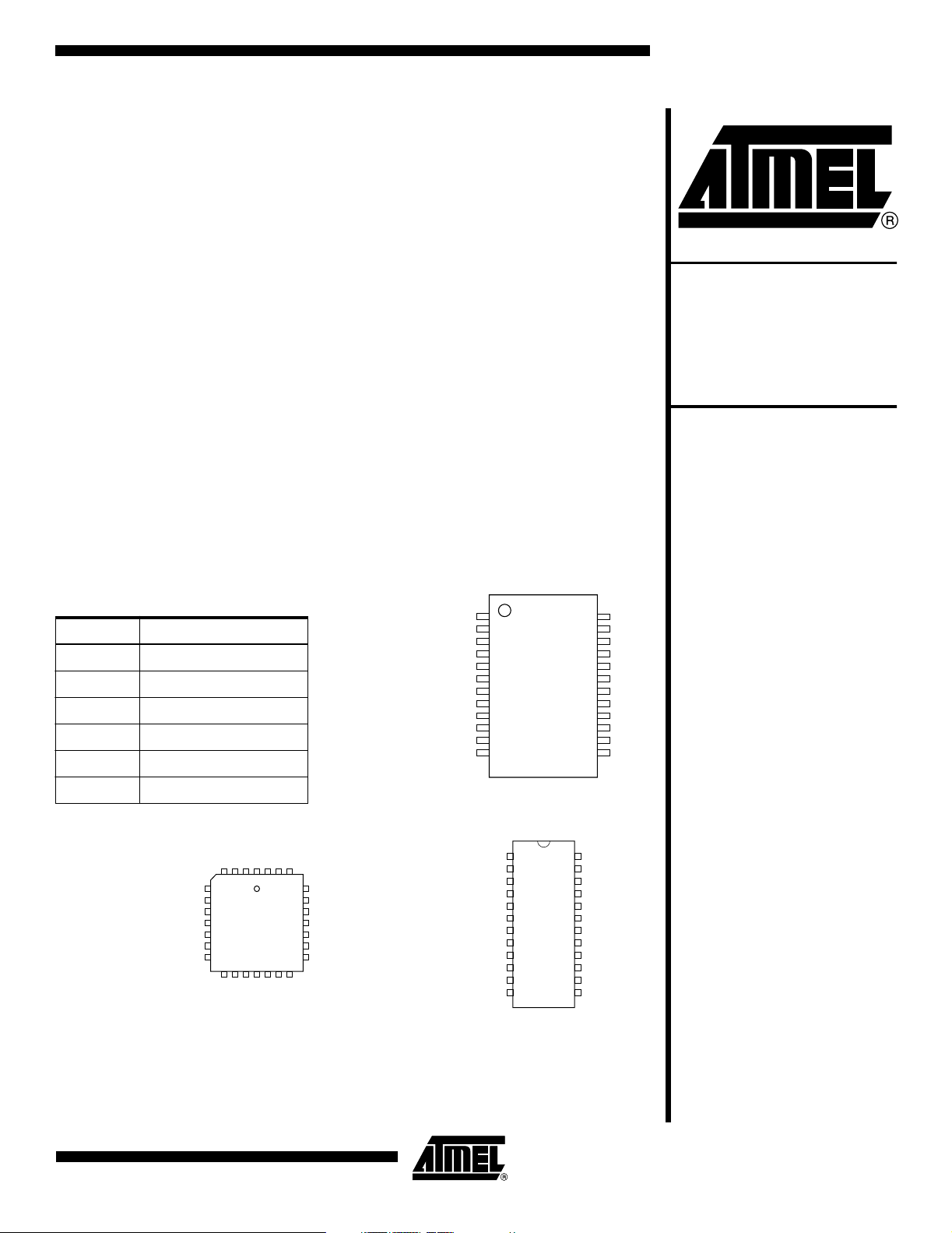
Pin Configurations
All Pinouts Top View
Pin Name Function
CLK Clock
IN Logic Inputs
I/O Bi-directional Buffers
GND Ground
VCC +5V Supply
CLK/IN
IN/PD
GND
IN
IN
IN
IN
IN
IN
IN
IN
IN
1
2
3
4
5
6
7
8
9
10
11
12
TSSOP
Highperformance
EE PLD
ATF22V10C
ATF22V10CQ
See separate datasheet
for ATF22V10CZ and
ATF22V10CQZ options.
24
VCC
23
I/O
22
I/O
21
I/O
20
I/O
19
I/O
18
I/O
17
I/O
16
I/O
15
I/O
14
I/O
13
IN
PD Power-down
PLCC
ININCLK/IN
VCC*
VCC
I/O
I/O
432
1
282726
IN/PD
GND*
IN
IN
IN
IN
IN
5
6
7
8
9
10
11
12131415161718
IN
IN
GND
GND*
I/O
25
I/O
24
I/O
23
GND*
22
I/O
21
I/O
20
I/O
19
IN
I/O
I/O
Note: For all PLCCs (except “-5”), pins 1, 8, 15 and 22 can be
left unconnected. However, if they are connected, superior performance will be achieved.
CLK/IN
IN/PD
GND
DIP/SOIC
1
2
IN
3
IN
4
5
IN
6
IN
7
IN
8
IN
9
IN
10
IN
11
IN
12
24
VCC
23
I/O
22
I/O
21
I/O
20
I/O
19
I/O
18
I/O
17
I/O
16
I/O
15
I/O
14
I/O
13
IN
Rev. 0735P–PLD–01/0 2
1
Page 2
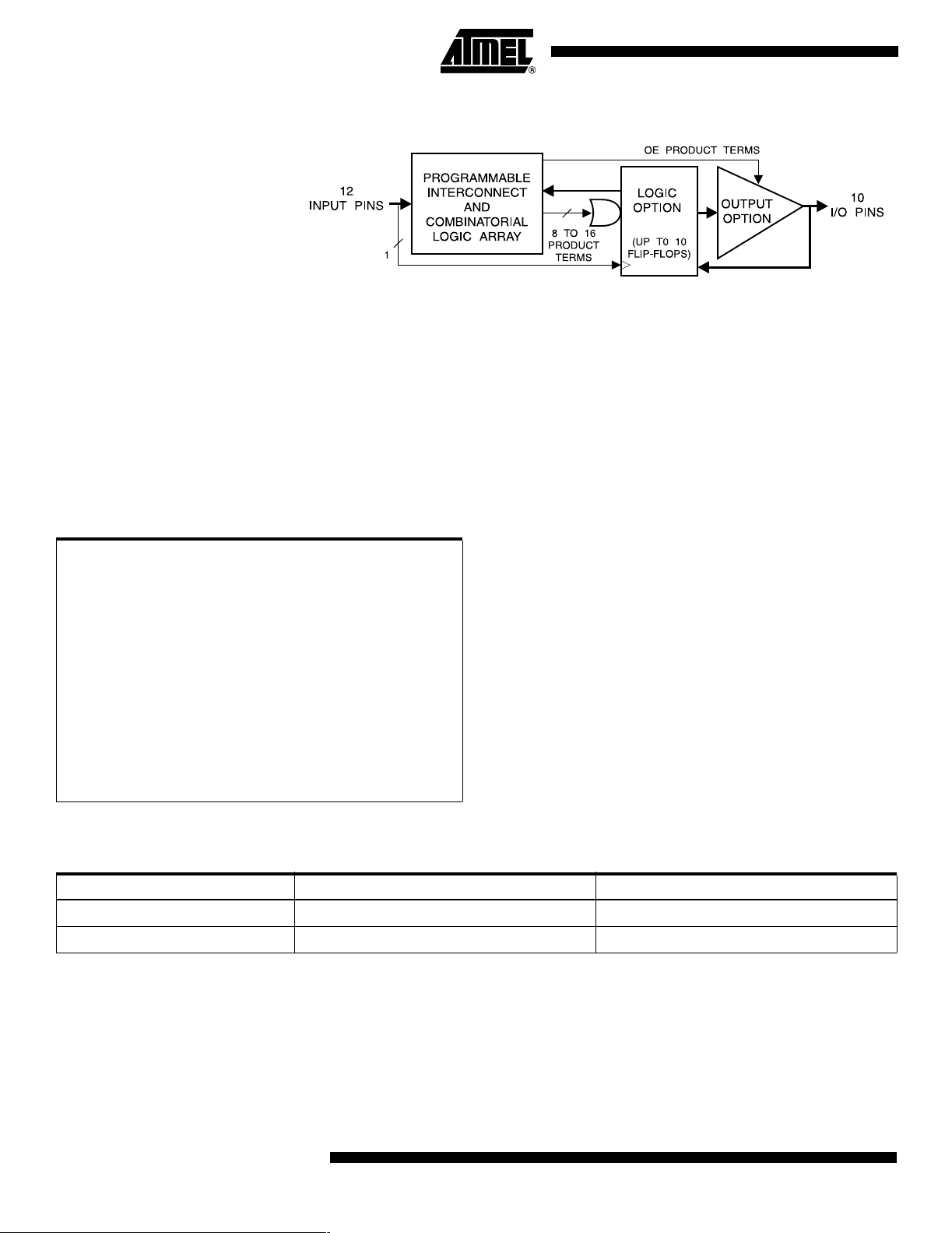
Logic Diagram
Description
The ATF22V10C is a high-performance CMOS (electrically erasable) programmable
logic device (PLD) that utilizes Atmel’s proven electrically erasable Flash memory technology. Speeds down to 5 ns and power dissipation as low as 100 µA are offered. All
speed ranges are specified over the full 5V ± 10% range for industrial temperature
ranges, and 5V ± 5% for commercial temperature ranges.
Several low-power options allow selection of the best solution for various types of
power-limited applications. Each of these options significantly reduces total system
power and enhances system reliability.
Absolute Maximum Ratings*
Temperature under Bias .................................. -40°Cto+85°C
Storage Temperature ..................................... -65°Cto+150°C
Voltage on Any Pin with
Respect to Ground .........................................-2.0V to +7.0V
Voltage on Input Pins
with Respect to Ground
during Programming ..................................... -2.0V to +14.0V
Programming Voltage with
Respect to Ground .......................................-2.0V to +14.0V
*NOTICE: Stresses beyond those listed under “Absolute
Maximum Ratings” may cause permanent damage to the device. This is a stress rating only and
functional operation of the device at these or any
(1)
(1)
Note: 1. Minimum voltage is -0.6V DC, which may under-
(1)
other conditions beyond those indicated in the
operational sections of this specification is not
implied. Exposure to absolute maximum rating
conditions for extended periods may affect device
reliability.
shoot to -2.0V for pulses of less than 20 ns.
Maximum output pin voltage is V
which may overshoot to 7.0V for pulses of less
than 20 ns.
+ 0.75V DC,
CC
DC and AC Operating Conditions
Commercial Industrial
Operating Temperature (Ambient) 0°C-70°C-40°C-85°C
V
Power Supply 5V ±5% 5V ± 10%
CC
2
ATF22V10C(Q)
0735P–PLD–01/02
Page 3
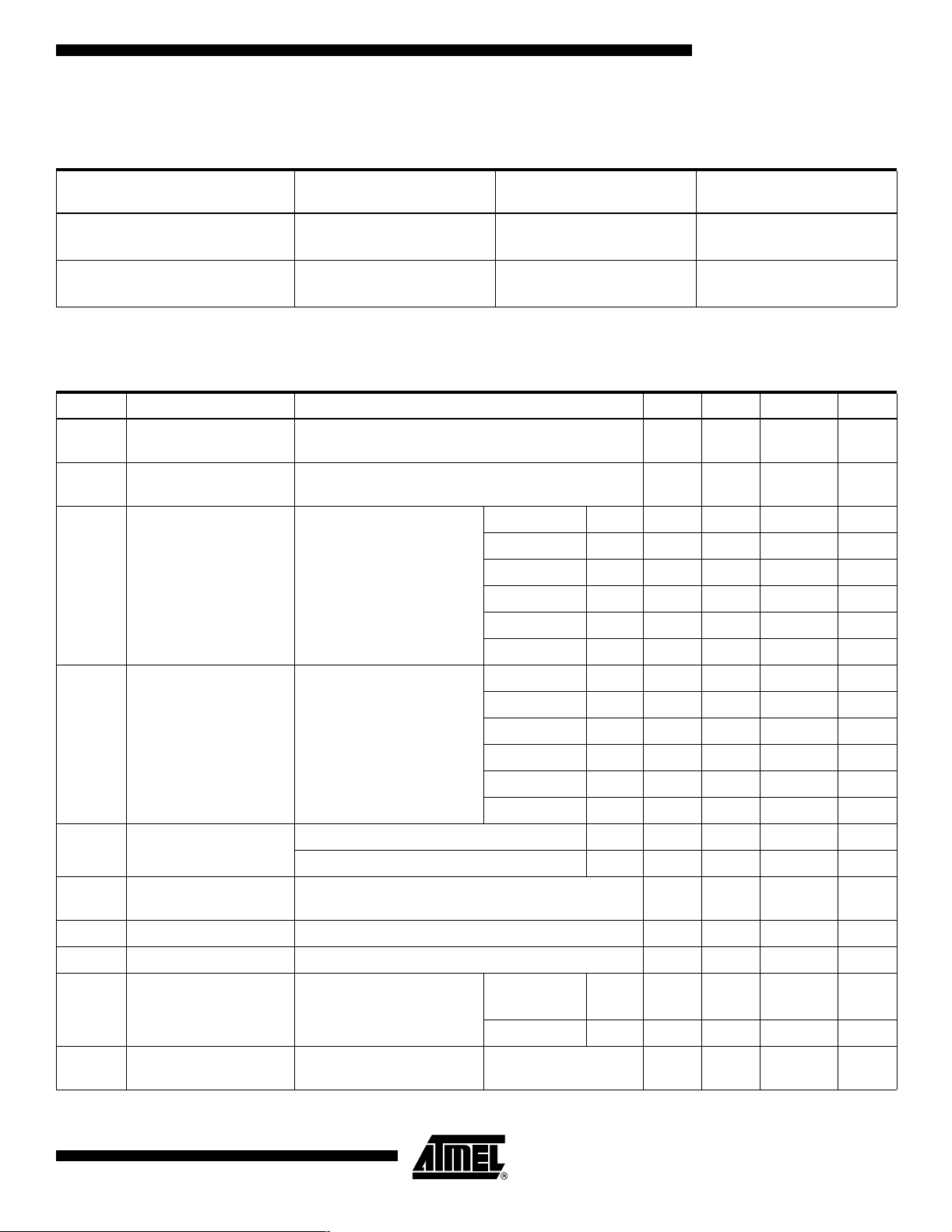
Compiler Mode Selection
PAL Mode
(5828 Fuses)
GAL Mode
(5892 Fuses)
ATF22V10C(Q)
Power-down Mode
(5893 Fuses)
(1)
Synario ATF22V10C (DIP)
ATF22V10C (PLCC)
WINCUPL P22V10
P22V10LCC
ATTF22V10C DIP (UES)
ATF22C10C PLCC (UES)
G22V10
G22V10LCC
ATF22V10C DIP (PWD)
ATF22V10C PLCC (PWD)
G22V10CP
G22V10CPLCC
Note: 1. These device types will create a JEDEC file which when programmed in ATF22V10C devices will enable the power-down
mode feature. All other device types have the feature disabled.
DC Characteristics
Symbol Parameter Condition Min Typ Max Units
I
IL
I
IH
I
CC
Input or I/O Low
Leakage Current
Input or I/O High
Leakage Current
Power Supply Current,
Standby
0 ≤ V
≤ VIL(Max) -35.0 -10.0 µA
IN
3.5 ≤ V
≤ V
IN
CC
C-5, 7, 10 Com. 85.0 130.0 mA
C-10 Ind. 90.0 140.0 mA
V
=Max,
CC
V
=Max,
IN
Outputs Open
C-15 Com. 65.0 90.0 mA
C-15 Ind. 65.0 115.0 mA
CQ-15 Com. 35.0 55.0 mA
CQ-15 Ind. 35.0 70.0 mA
C-5, 7, 10 Com. 150.0 mA
10.0 µA
C-10 Ind. 160.0 mA
I
CC2
Clocked Power Supply
Current
VCC= Max, Outputs Open,
f=15MHz
C-15 Com. 70.0 90.0 mA
C-15 Ind. 70.0 90.0 mA
CQ-15 Com. 40.0 60.0 mA
CQ-15 Ind. 40.0 80.0 mA
V
= Max Com. 10.0 100.0 µA
I
PD
(1)
I
OS
V
IL
V
IH
V
OL
V
OH
Power Supply Current,
PD Mode
Output Short Circuit
Current
Input Low Voltage -0.5 0.8 V
Input High Voltage 2.0 VCC+0.75 V
Output Low Voltage
Output High Voltage
CC
V
= 0, Max Ind. 10.0 100.0 µA
IN
V
= 0.5V -130.0 mA
OUT
V
IN=VIH
V
CC
V
IN=VIH
V
CC
=Min
=Min
or VIL,
or VIL,
I
=16mA
OL
=12mA Mil. 0.5 V
I
OL
=-4.0mA 2.4 V
I
OH
Com.,
Ind.
0.5 V
Note: 1. Not more than one output at a time should be shorted. Duration of short circuit test should not exceed 30 sec.
0735P–PLD–01/02
3
Page 4
AC Waveforms
(1)
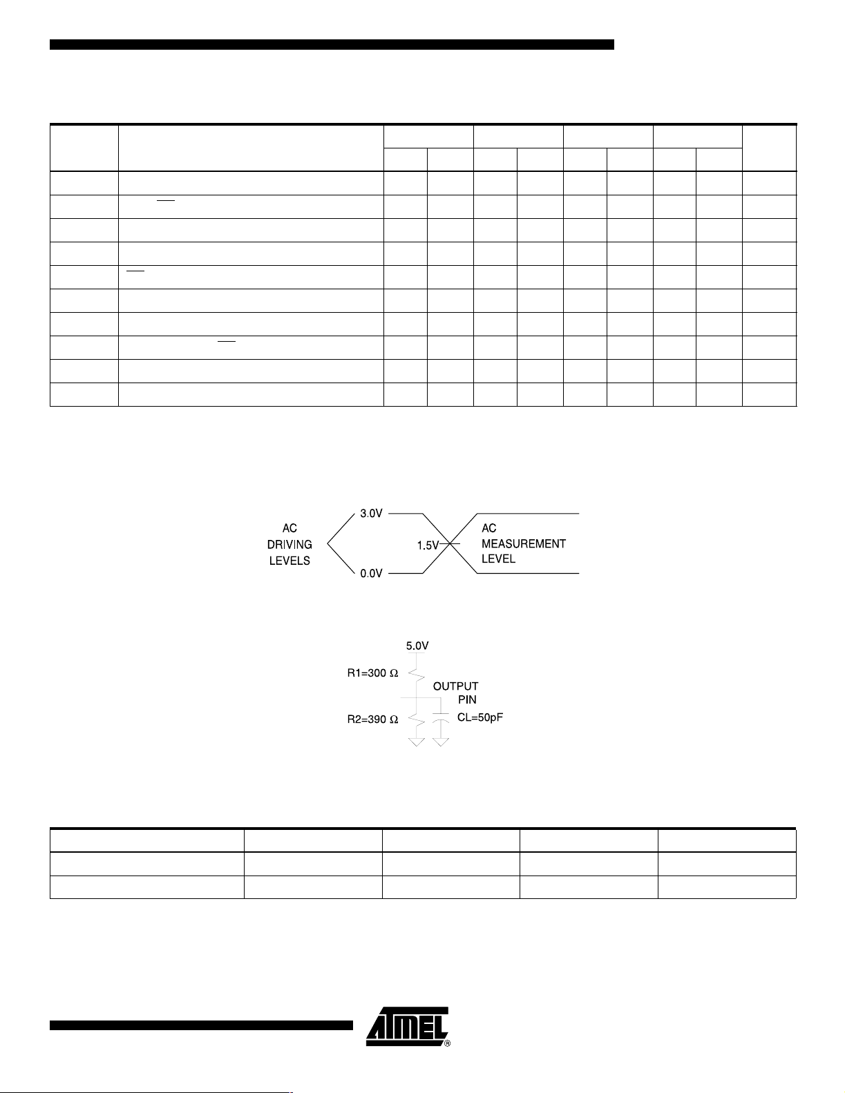
Note: 1. Timing measurement reference is 1.5V. Input AC driving levels are 0.0V and 3.0V, unless otherwise specified.
AC Characteristics
(1)
Symbol Parameter
t
PD
Input or Feedback to Combinatorial
1.0 5.0 3.0 7.5 3.0 10.0 3.0 15.0 ns
Output
t
CO
t
CF
t
S
t
H
Clock to Output 1.0 4.0 2.0 4.5
Clock to Feedback 2.5 2.5 2.5 2.5 ns
Input or Feedback Setup Time 3.0 3.5 4.5 10.0 ns
Hold Time 0 0 0 0 ns
External Feedback 1/(tS+tCO) 142.0 125.0
f
t
t
t
t
MAX
W
EA
ER
AP
Internal Feedback 1/(t
No Feedback 1/(t
WH+tWL
) 166.0 142.0 117.0 80.0 MHz
S+tCF
) 166.0 166.0 125.0 83.3 MHz
Clock Width (tWLand tWH) 3.0 3.0 3.0 6.0 ns
Input or I/O to Output Enable 2.0 6.0 3.0 7.5 3.0 10.0 3.0 15.0 ns
Input or I/O to Output Disable 2.0 5.0 3.0 7.5 3.0 9.0 3.0 15.0 ns
Input or I/O to Asynchronous Reset of
3.0 7.0 3.0 10.0 3.0 12.0 3.0 20.0 ns
Register
t
t
t
t
AW
AR
SP
SPR
Asynchronous Reset Width 5.5 7.0 8.0 15.0 ns
Asynchronous Reset Recovery Time 4.0 5.0 6.0 10.0 ns
Setup Time, Synchronous Preset 4.0 4.5 6.0 10.0 ns
Synchronous Preset to Clock
4.0 5.0 8.0 10.0 ns
Recovery Time
Notes: 1. See ordering information for valid part numbers.
2. 5.5 ns for DIP package devices.
3. 111 MHz for DIP package devices.
-5 -7 -10 -15
(2)
(3)
2.0 6.5 2.0 8.0 ns
90.0 55.5 MHz
UnitsMin Max Min Max Min Max Min Max
4
ATF22V10C(Q)
0735P–PLD–01/02
Page 5
ATF22V10C(Q)
Power-down AC Characteristics
(1)(2)(3)
-5 -7 -10 -15
Symbol Parameter
t
IVDH
t
GVDH
t
CVDH
t
DHIX
t
DHGX
t
DHCX
t
DLIV
t
DLGV
t
DLCV
t
DLOV
Valid Input before PD High 5.0 7.5 10.0 15.0 ns
Valid OE before PD High 0 0 0 0 ns
Valid Clock before PD High 0 0 0 ns
Input Don’t Care after PD High 5.0 7.0 10.0 15.0 ns
OE Don’t Care after PD High 5.0 7.0 10.0 15.0 ns
Clock Don’t Care after PD High 5.0 7.0 10.0 15.0 ns
PD Low to Valid Input 5.0 7.5 10.0 15.0 ns
PD Low to Valid OE 15.0 20.0 25.0 30.0 ns
PD Low to Valid Clock 15.0 20.0 25.0 30.0 ns
PD Low to Valid Output 20.0 25.0 30.0 35.0 ns
Notes: 1. Output data is latched and held.
2. High-Z outputs remain high-Z.
3. Clock and input transitions are ignored.
Input Test Waveforms and Measurement Levels
UnitsMin Max Min Max Min Max Min Max
Commercial Output Test Loads
Pin Capacitance
f=1MHz,T=25°C
C
IN
C
OUT
Note: 1. Typical values for nominal supply voltage. This parameter is only sampled and is not 100% tested.
(1)
Typ Max Units Conditions
58pFV
68pFV
IN
OUT
=0V
=0V
0735P–PLD–01/02
5
Page 6
Power-up Reset The registers in the ATF22V10Cs are designed to reset during power-up. At a point
delayed slightly from V
output state will depend on the polarity of the output buffer.
This feature is critical for state machine initialization. However, due to the asynchronous
nature of reset and the uncertainty of how V
conditions are required:
1. The V
rise must be monotonic, and starts below 0.7V,
CC
2. After reset occurs, all input and feedback setup times must be met before driving
the clock pin high, and
3. The clock must remain stable during t
POWER
crossing V
CC
, all registers will be reset to the low state. The
RST
actually rises in the system, the following
CC
.
PR
V
R
ST
t
PR
Preload of Registered Outputs
REGISTERED
OUTP UTS
C
LOCK
The ATF22V10C’s registers are provided with circuitry to allow loading of each register
with either a high or a low. This feature will simplify testing since any state can be forced
into the registers to control test sequencing. A JEDEC file with preload is generated
t
S
t
W
when a source file with vectors is compiled. Once downloaded, the JEDEC file preload
sequence will be done automatically by most of the approved programmers after the
programming.
Electronic Signature Word
There are 64 bits of programmable memory that are always available to the user, even if
the device is secured. These bits can be used for user-specific data.
Parameter Description Typ Max Units
t
PR
V
RST
Power-up Reset Time 600 1,000 ns
Power-up Reset Voltage 3.8 4.5 V
Security Fuse Usage A single fuse is provided to prevent unauthorized copying of the ATF22V10C fuse pat-
terns. Once programmed, fuse verify and preload are inhibited. However, the 64-bit
User Signature remains accessible.
Programming/ Erasing
6
ATF22V10C(Q)
The security fuse should be programmed last, as its effect is immediate.
Programming/erasing is performed using standard PLD programmers. See “CMOS PLD
Programming Hardware & Software Support” for information on software/programming.
0735P–PLD–01/02
Page 7

ATF22V10C(Q)
Input and I/O Pinkeeper Circuits
Input Diagram
The ATF22V10C contains internal input and I/O pin-keeper circuits. These circuits allow
each ATF22V10C pin to hold its previous value even when it is not being driven by an
external source or by the device’s output buffer. This helps to ensure that all logic array
inputs are at known valid logic levels. This reduces system power by preventing pins
from floating to indeterminate levels. By using pin-keeper circuits rather than pull-up
resistors, there is no DC current required to hold the pins in either logic state (high or
low).
These pin-keeper circuits are implemented as weak feedback inverters, as shown in the
Input Diagram below. These keeper circuits can easily be overdriven by standard TTLor CMOS-compatible drivers. The typical overdrive current required is 40 µA.
I/O Diagram
0735P–PLD–01/02
7
Page 8

Power-down Mode The ATF22V10C includes an optional pin-controlled power-down feature. When this
mode is enabled, the PD pin acts as the power-down pin (Pin 4 on the DIP/SOIC packages and Pin 5 on the PLCC package). When the PD pin is high, the device supply
current is reduced to less than 100 mA. During power-down, all output data and internal
logic states are latched and held. Therefore, all registered and combinatorial output data
remain valid. Any outputs that were in an undetermined state at the onset of powerdown will remain at the same state. During power-down, all input signals except the
power-down pin are blocked. Input and I/O hold latches remain active to ensure that
pins do not float to indeterminate levels, further reducing system power. The powerdown pin feature is enabled in the logic design file. Designs using the power-down pin
may not use the PD pin logic array input. However, all other PD pin macrocell resources
may still be used, including the buried feedback and foldback product term array inputs.
PD pin configuration is controlled by the design file, and appears as a separate fuse bit
in the JEDEC file. When the power-down feature is not specified in the design file, the
IN/PD pin will be configured as a regular logic input.
Note: Some programmers list the 22V10 JEDEC compatible 22V10C (no PD used) separately
from the non-22V10 JEDEC compatible 22V10CEX (with PD used).
8
ATF22V10C(Q)
0735P–PLD–01/02
Page 9

Functional Logic Diagram ATF22V10C
ATF22V10C(Q)
0735P–PLD–01/02
9
Page 10

ATF22V10C/CQSUPPLY CURRENT VS.
140.0
SUPPLY VOLTAGE (T
120.0
100.0
80.0
(mA)
60.0
CC
I
40.0
20.0
0.0
4.50 4.75 5. 00 5.25 5.50
SUPPLY VOLTAGE (V)
= 25°C)
A
C-5, -7, -10
C-15
CQ-15
ATF22V10C/CQ NORMALIZED ICCVS.
1.1
CC
1.0
0.9
NORMALIZED I
0.8
-40.0 0.0 25.0 75.0
TEMPERATURE
TE MP ERATURE (°C)
ATF22V10C/CQ SUPPLY CURRENT VS.
INPUT FREQUENCY (V
80.0
40.0
0.0
0.0 10.0 20. 0 50.0
FREQUENCY (MHz)
(mA)
CC
I
120.0
=5V,TA= 25°C)
CC
C-5, 7, 10
C-15
ATF22V10C/CQ OUTPUT SOURCE CURRENT VS.
0.0
SUPPLY VOLTAGE (V
-5.0
-10.0
-15.0
-20.0
-25.0
(mA)
-30.0
OH
I
-35.0
-40.0
-45.0
-50.0
4.0 4.5 5.0 5.5 6.0
SUPPLY VOLTAGE (V)
OH
=2.4V)
CQ-15
ATF22V10C/CQ OUTPUT SOURCE CURRENT VS.
0.0
OUT PU T VOLT A GE (V
-10.0
-20.0
-30.0
-40.0
(mA)
-50.0
OH
I
-60.0
-70.0
-80.0
-90.0
0.00.51.01.52.02.53.03.54.04.55.0
=5V,TA=25°C)
CC
V
(V)
OH
ATF22V10C/CQ OUTPUT SINK CURRENT VS.
140.0
SUPPLY VOLTAGE (V
120.0
100.0
80.0
(mA)
60.0
OL
I
40.0
20.0
0.0
0.0 0.5 1.0 1.5 2.0 2.5 3.0 3.5 4.0 4.5 5.0
SUPPLY VOLTAGE (V)
OL
=0.5V)
10
ATF22V10C/CQ OUTPUT SINK CURRENT VS.
46.0
SUPPLY VOLTAGE (V
45.0
44.0
43.0
42.0
(mA)
41.0
OL
I
40.0
39.0
38.0
37.0
4.0 4. 5 5.0 5.5 6.0
SUPPLY VOLTAGE (V)
OL
=0.5V)
ATF22V10C(Q)
ATF22V10C/CQ INPUT CLAMP CURRENT VS.
0.0
INPUT VOLTAGE (V
-20.0
-40.0
-60.0
-80.0
-100. 0
INPUT CURRENT mA)
-120. 0
0.0 -0.2-0.4 -0.6-0.8-1.0
INPUT VOLTAGE (V)
=5V,TA=35°C)
CC
0735P–PLD–01/02
Page 11

ATF22V10C(Q)
ATF22V10C/CQ NORMALIZED TPDVS. V
1.2
PD
1.1
1.0
0.9
NORMALIZED T
0.8
4.50 4.75 5.00 5. 25 5.50
SUPPLY VOLTAGE (V)
ATF22V10C/CQ NORMALIZED TCOVS. V
1.3
CO
1.2
1.1
1.0
0.9
NORMALIZED T
0.8
4.50 4.75 5.00 5. 25 5.50
SUPPLY VOLTAGE (V)
CC
1.1
CO
1.0
0.9
NORMALIZED T
0.8
-40.0 0.0 25.0 75.0
CC
1.1
CO
1.0
0.9
NORMALIZED T
0.8
-40.0 0.0 25.0 75 .0
ATF22V10C/CQ NORMALIZED TCOVS.
TEMPERATURE
TEMPERATURE (°C)
ATF22V 10C/CQ NORMALIZED TSUVS.
TEMPERATURE
TE MP ERATURE (°C)
ATF22V10C/CQ NORMALIZED TSUVS. V
1.2
SU
1.1
1.0
0.9
NORMALIZED T
0.8
4.50 4.75 5. 00 5. 25 5. 50
SUPPLY VOLTAGE (V)
CC
ATF22V10C/CQNORMALIZED TPDVS.
1.1
PD
1.0
0.9
NORMALIZED T
0.8
-40.0 0.0 25.0 75.0
TEMPERATURE
TEMPERATURE (°C)
ATF22V 10C/CQ DELTA TPDVS.
8.0
6.0
(ns)
4.0
PD
2.0
DELTA T
0.0
-2.0
0 50 100 150 200 250 300
OUTPUT LOADING
OUTPUT LOADING (pF)
ATF22V 10C/CQ DELTA TPDVS.
0.0
-0.1
(ns)
-0.2
PD
-0.3
-0.4
DELTA T
-0.5
1.02.03.04.05.06.07.08.09.010.0
NU MB ER OF OU TPUT S WITCHING
NUMBE R OF OUT PUT S SWI TCHI NG
0735P–PLD–01/02
11
Page 12

ATF22V10C/CQ DELTA TCOVS.
8.0
7.0
6.0
(ns)
5.0
CO
4.0
3.0
2.0
DELTA T
1.0
0.0
50 100 150 200 250 300
OUTPUT LOADING
NUMBE R OF OUT PUT S LOADING
ATF22V 10C/CQ DELTA TCOVS.
0.0
-0.1
-0.2
(ns)
CO
-0.3
-0.4
DELTA T
-0.5
-0.6
1.02.03.04.05.06.07.08.09.010.0
NUMBER OF SWITCHING
NUMBE R OF OUT PUT S SWI TCHI NG
12
ATF22V10C(Q)
0735P–PLD–01/02
Page 13

ATF22V10C(Q)
ATF22V10C(Q) Ordering Information
tPD(ns) tS(ns) tCO(ns) Ordering Code Package Operation Range
5 3 4 ATF22V10C-5JC 28J Commercial
(0°Cto70°C)
7.5 3.5 4.5 ATF22V10C-7JC
ATF22V10C-7PC
ATF22V10C-7SC
ATF22V10C-7XC
ATF22V10C-7JI 28J Industrial
10 4.5 6.5 ATF22V10C-10JC
ATF22V10C-10PC
ATF22V10C-10SC
ATF22V10C-10XC
ATF22V10C-10JI
ATF22V10C-10PI
ATF22V10C-10SI
ATF22V10C-10XI
15 10 8 ATF22V10C-15JC
ATF22V10C-15PC
ATF22V10C-15SC
ATF22V10C-15XC
ATF22V10C-15JI
ATF22V10C-15PI
ATF22V10C-15SI
ATF22V10C-15XI
15 10 8 ATF22V10CQ-15JC
ATF22V10CQ-15PC
ATF22V10CQ-15SC
ATF22V10CQ-15XC
ATF22V10CQ-15JI
ATF22V10CQ-15PI
ATF22V10CQ-15SI
ATF22V10CQ-15XI
28J
24P3
24S
24X
28J
24P3
24S
24X
28J
24P3
24S
24X
28J
24P3
24S
24X
28J
24P3
24S
24X
28J
24P3
24S
24X
28J
24P3
24S
24X
Commercial
(0°Cto70°C)
(-40°Cto85°C)
Commercial
(0°Cto70°C)
Industrial
(-40°Cto85°C)
Commercial
(0°Cto70°C)
Industrial
(-40°Cto85°C)
Commercial
(0°Cto70°C)
Industrial
(-40°Cto85°C)
Using “C” Product for Industrial
To use commercial product for Industrial temperature ranges, down-grade one speed grade from the “I” to the “C” device
(7 ns “C” =10ns“I”) and de-rate power by 30%.
Package Type
28J 28-lead, Plastic J-leaded Chip Carrier (PLCC)
24P3 24-pin, 0.300" Wide, Plastic Dual Inline Package (PDIP)
24S 24-lead, 0.300" Wide, Plastic Gull Wing Small Outline (SOIC)
24X 24-lead, 4.4 mm Wide, Plastic Thin Shrink Small Outline (TSSOP)
0735P–PLD–01/02
13
Page 14

Packaging Information
1.14(0.045) X 45˚
PIN NO. 1
IDENTIFIER
1.14(0.045) X 45˚
0.51(0.020)MAX
0.318(0.0125)
0.191(0.0075)
A2
28J–PLCC
B
E1 E
e
D1
D
45˚ MAX (3X)
Notes: 1. This package conforms to JEDEC reference MS-018, Variation AB.
2. Dimensions D1 and E1 do not include mold protrusion.
Allowable protrusion is .010"(0.254 mm) per side. Dimension D1
and E1 include mold mismatch and are measured at the extreme
material condition at the upper or lower parting line.
3. Lead coplanarity is 0.004" (0.102 mm) maximum.
B1
A1
A
COMMON DIMENSIONS
(Unit of Measure = mm)
SYMBOL
A 4.191 – 4.572
A1 2.286 – 3.048
A2 0.508 – –
D 12.319 – 12.573
D1 11.430 – 11.582 Note 2
E 12.319 – 12.573
E1 11.430 – 11.582 Note 2
D2/E2 9.906 – 10.922
B 0.660 – 0.813
B1 0.330 – 0.533
e 1.270 TYP
MIN
NOM
MAX
D2/E2
NOTE
R
14
ATF22V10C(Q)
2325 Orchard Parkway
San Jose, CA 95131
TITLE
28J, 28-lead, Plastic J-leaded Chip Carrier (PLCC)
DRAWING NO.
28J
0735P–PLD–01/02
10/04/01
REV.
B
Page 15

24P3 – PDIP
PIN
1
E1
A1
B
E
B1
C
L
SEATING PLANE
A
ATF22V10C(Q)
D
e
eC
eB
Notes: 1. This package conforms to JEDEC reference MS-001, Variation AF.
2. Dimensions D and E1 do not include mold Flash or Protrusion.
Mold Flash or Protrusion shall not exceed 0.25 mm (0.010").
TITLE
2325 Orchard Parkway
R
San Jose, CA 95131
24P3, 24-lead (0.300"/7.62 mm Wide) Plastic Dual
Inline Package (PDIP)
COMMON DIMENSIONS
(Unit of Measure = mm)
SYMBOL
A ––5.334
A1 0.381 ––
D 31.623 – 32.131 Note 2
E 7.620 – 8.255
E1 6.096 – 7.112 Note 2
B 0.356 – 0.559
B1 1.270 – 1.551
L 2.921 – 3.810
C 0.203 – 0.356
eB ––10.922
eC 0.000 – 1.524
e 2.540 TYP
MIN
NOM
MAX
DRAWING NO.
24P3
NOTE
09/28/01
REV.
C
0735P–PLD–01/02
15
Page 16

24S – SOIC
Dimensions in Millimeters and (Inches)
Controlling dimension: Inches
JEDEC STANDARD MS-013
0.51 (0.020)
0.33 (0.013)
PIN 1 ID
PIN 1
15.60(0.6141)
15.20(0.5985)
0º ~ 8º
7.60(0.2992)
7.40(0.2914)
1.27(0.050) BSC
0.30(0.0118)
0.10(0.0040)
10.65(0.419)
10.00(0.394)
2.65(0.1043)
2.35(0.0926)
0.32(0.0125)
0.23(0.0091)
16
2325 Orchard Parkway
R
San Jose, CA 95131
TITLE
24S, 24-lead (0.300" body) Plastic Gull Wing Small Outline (SOIC)
ATF22V10C(Q)
1.27(0.050)
0.40(0.016)
04/11/2001
DRAWING NO.
24S
0735P–PLD–01/02
REV.
A
Page 17

24X – TSSOP
Dimensions in Millimeter and (Inches)*
JEDEC STANDARD MO-153 AD
Controlling dimension: millimeters
ATF22V10C(Q)
0.30(0.012)
0.19(0.007)
PIN 1
0º ~ 8º
7.90(0.311)
7.70(0.303)
4.48(0.176)
4.30(0.169)
0.65(0.0256)BSC
0.15(0.006)
0.05(0.002)
6.50(0.256)
6.25(0.246)
1.20(0.047)MAX
0.20(0.008)
0.09(0.004)
2325 Orchard Parkway
R
San Jose, CA 95131
0735P–PLD–01/02
0.75(0.030)
0.45(0.018)
TITLE
24X, 24-lead (4.4 mm body width) Plastic Thin Shrink Small Outline
Package (TSSOP)
04/11/2001
DRAWING NO.
24X
REV.
A
17
Page 18

Atmel Headquarters Atmel Operations
Corporate Headquarters
2325 Orchard Parkway
San Jose, CA 95131
TEL 1(408) 441-0311
FAX 1(408) 487-2600
Europe
Atmel SarL
Route des Arsenaux 41
Casa Postale 80
CH-1705 Fribourg
Switzerland
TEL (41) 26-426-5555
FAX (41) 26-426-5500
Asia
Atmel Asia, Ltd.
Room 1219
Chinachem Golden Plaza
77 Mody Road Tsimhatsui
East Kowloon
Hong Kong
TEL (852) 2721-9778
FAX (852) 2722-1369
Japan
Atmel Japan K.K.
9F, Tonetsu Shinkawa Bldg.
1-24-8 Shinkawa
Chuo-ku, Tokyo 104-0033
Japan
TEL (81) 3-3523-3551
FAX (81) 3-3523-7581
Memory
Atmel Corporate
2325 Orchard Parkway
San Jose, CA 95131
TEL 1(408) 436-4270
FAX 1(408) 436-4314
Microcontrollers
Atmel Corporate
2325 Orchard Parkway
San Jose, CA 95131
TEL 1(408) 436-4270
FAX 1(408) 436-4314
Atmel Nantes
La Chantrerie
BP 70602
44306 Nantes Cedex 3, France
TEL (33) 2-40-18-18-18
FAX (33) 2-40-18-19-60
ASIC/ASSP/Smart Cards
Atmel Rousset
Zone Industrielle
13106 Rousset Cedex, France
TEL (33) 4-42-53-60-00
FAX (33) 4-42-53-60-01
Atmel Colorado Springs
1150 East Cheyenne Mtn. Blvd.
Colorado Springs, CO 80906
TEL 1(719) 576-3300
FAX 1(719) 540-1759
RF/Automotive
Atmel Heilbronn
Theresienstrasse 2
Postfach 3535
74025 Heilbronn, Germany
TEL (49) 71-31-67-0
FAX (49) 71-31-67-2340
Atmel Colorado Springs
1150 East Cheyenne Mtn. Blvd.
Colorado Springs, CO 80906
TEL 1(719) 576-3300
FAX 1(719) 540-1759
Biometrics/Imaging/Hi-Rel MPU/
High Speed Converters/RF Datacom
Atmel Grenoble
Avenue de Rochepleine
BP 123
38521 Saint-Egreve Cedex, France
TEL (33) 4-76-58-30-00
FAX (33) 4-76-58-34-80
Atmel Smart Card ICs
Scottish Enterprise Technology Park
Maxwell Building
East Kilbride G75 0QR, Scotland
TEL (44) 1355-803-000
FAX (44) 1355-242-743
e-mail
literature@atmel.com
Web Site
http://www.atmel.com
© Atmel Corporation 2002.
Atmel Corporation makes no warranty for the use of its products, other than those expressly contained in the Company’s standard warranty
whichisdetailedinAtmel’s Terms and Conditions located on the Company’s web site. The Company assumes no responsibility for any errors
which may appear in this document, reserves the right to change devices or specifications detailed herein at any time without notice, and does
not make any commitment to update the information contained herein. No licenses to patents or other intellectual property of Atmel are granted
by the Company in connection with the sale of Atmel products, expressly or by implication. Atmel’s products are not authorized for use as critical
components in life support devices or systems.
Atmel®is a registered trademark of Atmel.
Terms and product names in this document may be trademarks of others.
Printed on recycled paper.
0735P–PLD–01/02 0M
 Loading...