

Page 1
Features
• 3.0V to 5.5V Operating Range
• Lowest Power in It Class
• Advanced Low-voltage, Zero-power, Electrically Erasable Programmable Logic Device
• “Zero” Standby Power (25 µA Maximum) (Input Transition Detection)
• Low-voltage Equivalent of ATF22V10CZ
• Ideal for Battery Powered Systems
• CMOS- and TTL-compatible Inputs and Outputs
• Inputs are 5V Tolerant
• Latch Feature Hold Inputs to Previous Logic States
• EE Technology
– Reprogrammable
– 100% Tested
• High-reliability CMOS Process
– 20-year Data Retention
– 10,000 Erase/Write Cycles
– 2,000V ESD Protection
– 200 mA Latch-up Immunity
• Commercial and Industrial Temperature Ranges
• Dual Inline and Surface Mount Standard Pinouts
Highperformance
EE PLD
ATF22LV10CZ
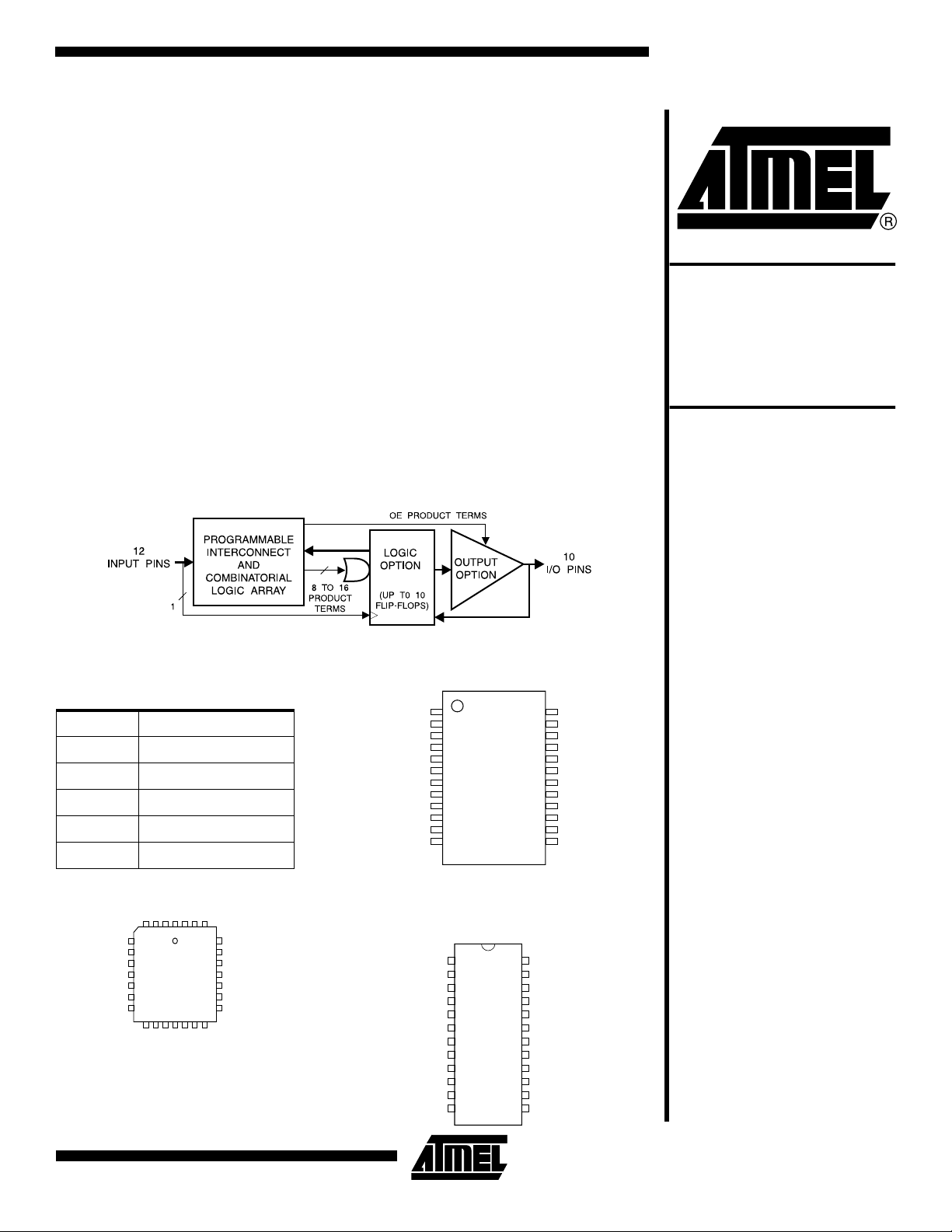
Block Diagram
Pin Configurations
All Pinouts Top View
Pin Name Function
CLK Clock
IN Logic Inputs
I/O Bi-directional Buffers
GND Ground
VCC (3 to 5.5V) Supply
PLCC
ININCLK/IN
VCC*
VCC
I/O
I/O
432
1
282726
GND*
I/O
25
I/O
24
I/O
23
GND*
22
I/O
21
I/O
20
I/O
19
IN
I/O
I/O
5
IN
6
IN
7
IN
8
GND*
9
IN
10
IN
11
IN
12131415161718
IN
IN
GND
Note: For PLCC, pins 1, 8, 15, and
22 can be left unconnected.
For superior performance,
connect VCC to pin 1 and
GND to pins 8, 15, and 22.
TSSOP
1
CLK/IN
GND
2
IN
3
IN
4
IN
5
IN
6
IN
7
IN
8
IN
9
IN
10
IN
11
IN
12
24
VCC
23
I/O
22
I/O
21
I/O
20
I/O
19
I/O
18
I/O
17
I/O
16
I/O
15
I/O
14
I/O
13
IN
Note: TSSOP is the smallest package
of SPLD offering.
DIP/SOIC
CLK/IN
GND
1
2
IN
3
IN
4
IN
5
IN
6
IN
7
IN
8
IN
9
IN
10
IN
11
IN
12
24
VCC
23
I/O
22
I/O
21
I/O
20
I/O
19
I/O
18
I/O
17
I/O
16
I/O
15
I/O
14
I/O
13
IN
ATF22LV10CQZ
Rev. 0779K–04/01
1
Page 2
Description
The ATF22LV10CZ/CQZ is a high-performance CMOS
(electrically erasable) programmable logic device (PLD)
that utilizes Atmel’s proven electrically erasable Flash
memory technology and provides 25 ns speed with standby
current of 25 µA maximum. All speed ranges are specified
over the 3.0V to 5.5V range for industrial and commercial
temperature ranges.
The ATF22LV10CZ/CQZ provides a low-voltage and edgesensing “zero” power CMOS PLD solution with “zero”
standby power (5 µA typical). The ATF22LV10CZ/CQZ
powers down automatically to the zero power mode
through Atmel’s patented Input Transition Detection (ITD)
circuitry when the device is idle. The ATF22LV10CZ/CQZ
is capable of operating at supply voltages down to 3.0V.
Absolute Maximum Ratings*
Temperature under Bias .................................. -40°C to +85°C
Storage Temperature ..................................... -65°C to +150°C
Voltage on Any Pin with
Respect to Ground .........................................-2.0V to +7.0V
Voltage on Input Pins
with Respect to Ground
during Programming .....................................-2.0V to +14.0V
Programming Voltage with
Respect to Ground .......................................-2.0V to +14.0V
(1)
(1)
(1)
Pin “keeper” circuits on input and output pins hold pins to
their previous logic levels when idle, which eliminate static
power consumed by pull-up resistors. The “CQZ” combines
this low high-frequency I
of the “Q” design with the “Z”
CC
feature.
The ATF22LV10CZ/CQZ macrocell incorporates a variable
product term architecture. Each output is allocated from 8
to 16 product terms which allows highly complex logic functions to be realized. Two additional product terms are
included to provide synchronous reset and asynchronous
reset. These additional product terms are common to all 10
registers and are automatically cleared upon power-up.
Register Preload simplifies testing. A security fuse prevents
unauthorized copying of programmed fuse patterns.
*NOTICE: Stresses beyond those listed under “Absolute
Maximum Ratings” may cause permanent damage to the device. This is a stress rating only and
functional operation of the device at these or any
other conditions beyond those indicated in the
operational sections of this specification is not
implied. Exposure to absolute maximum rating
conditions for extended periods may affect device
reliability.
Note: 1. Minimum voltage is -0.6V DC, which may under-
shoot to -2.0V for pulses of less than 20 ns.
Maximum output pin voltage is V
which may overshoot to 7.0V for pulses of less
than 20 ns.
+ 0.75V DC,
CC
DC and AC Operating Conditions
Commercial Industrial
Operating Temperature (Ambient) 0°C - 70°C-40°C - 85°C
V
Power Supply 3.0V - 5.5V 3.0V - 5.5V
CC
2
ATF22LV10C(Q)Z
Page 3
Functional Logic Diagram Description
The Functional Logic Diagram describes the
ATF22LV10CZ/CQZ architecture.
The ATF22LV10CZ/CQZ has 12 inputs and 10 I/O macrocells. Each macrocell can be configured into one of four
output configurations: active high/low or registered/combinatorial. The universal architecture of the
ATF22LV10CZ/CQZ can be programmed to emulate most
24-pin PAL devices.
DC Characteristics
Symbol Parameter Condition
(2)
ATF22LV10C(Q)Z
Unused product terms are automatically disabled by the
compiler to decrease power consumption. A security fuse,
when programmed, protects the contents of the
ATF22LV10CZ/CQZ. Eight bytes (64 fuses) of User Signature are accessible to the user for purposes such as storing
project name, part number, revision or date. The User
Signature is accessible regardless of the state of the
security fuse.
Min Typ Max Units
I
IL
I
IH
Input or I/O Low
Leakage Current
Input or I/O High
Leakage Current
0 ≤ V
≤ V
IN
- 0.2)V ≤ VIN ≤ V
(V
CC
(Max) -10.0 µA
IL
CC
10.0 µA
CZ-25 Com. 50.0 85.0 mA
= Max
V
I
CC
Clocked Power
Supply Current
CC
Outputs Open,
f = 15 MHz
CZ-25 Ind.
CQZ-30 Com.
CQZ-30 Ind.
55.0 90.0 mA
18.0 50.0 mA
19.0 60.0 mA
CZ-25 Com. 3.0 25.0 µA
V
= Max
I
SB
(1)
I
OS
V
IL
V
IH
V
OL
V
OH
V
OH
Power Supply Current,
Standby
Output Short Circuit
Current
Input Low Voltage -0.5 0.8 V
Input High Voltage 2.0 VCC + 0.75 V
Output Low Voltage
Output High Voltage
Output High Voltage IOH = -100 µA VCC - 0.2V V
CC
= Max
V
IN
Outputs Open
= 0.5V -130.0 mA
V
OUT
= VIH or V
V
IN
IL
VCC = Min,
= 16 mA
I
OL
= VIH or V
V
IN
V
CCIO
= -2.0 mA
I
OH
= Min,
IL
CZ-25 Ind.
CQZ-30 Com.
CQZ-30 Ind.
4.0 50.0 µA
3.0 25.0 µA
4.0 50.0 µA
0.5 V
2.4 V
Notes: 1. Not more than one output at a time should be shorted. Duration of short circuit test should not exceed 30 sec.
2. For DC characterization, the test condition of V
= Max corresponds to 3.6V.
CC
3
Page 4
AC Waveforms
REG. FEEDBACK
SYNCH. PRESET
ASYNCH. RESET
INPUTS, I/O
CP
tS
tH
tW tW
tP
tAW
tAR
REGISTERED
OUTPUTS
tPD
COMBINATORIAL
OUTPUTS
AC Characteristics
(1)
Symbol Parameter
t
PD
t
CF
t
CO
t
S
t
H
t
P
t
W
Input or Feedback to Non-registered Output 3.0 25.0 10.0 30.0 ns
Clock to Feedback 13.0 10.0 15.0 ns
Clock to Output 2.0 15.0 4.0 20.0 ns
Input or Feedback Setup Time 15.0 18.0 ns
Input Hold Time 0 0 ns
Clock Period 25.0 30.0 ns
Clock Width 12.5 15.0 ns
External Feedback 1/(tS + tCO)
f
MAX
t
EA
t
ER
t
AP
t
SP
t
AW
t
AR
t
SPR
Internal Feedback 1/(t
No Feedback 1/(t
Input to Output Enable 3.0 25.0 10.0 30.0 ns
Input to Output Disable 3.0 25.0 10.0 30.0 ns
Input or I/O to Asynchronous Reset of Register 3.0 25.0 10.0 3.0 ns
Setup Time, Synchronous Preset 15.0 20.0 ns
Asynchronous Reset Width 25.0 30.0 ns
Asynchronous Reset Recovery Time 25.0 30.0 ns
Synchronous Preset to Clock Recovery Time 15.0 20.0 ns
+ tCF)
S
)
P
Note: 1. See ordering information for valid part numbers.
tAPtCO
VALID
VALID VALID
VALID
33.3
35.7
40.0
tER tEA
OUTPUT
DISABLED
tEAtER
OUTPUT
DISABLED
VALID
VALID
-25 -30
25.0
30.0
33.3
UnitsMin Max Min Max
MHz
MHz
MHz
4
ATF22LV10C(Q)Z
Page 5

ATF22LV10C(Q)Z
Input Test Waveforms and
Output Test Loads
Measurement Levels
Note: Similar competitors devices are specified with slightly
different loads. These load differences may affect output
signals’ delay and slew rate. Atmel devices are tested
with sufficient margins to meet compatible device specification conditions.
Pin Capacitance
f = 1 MHz, T = 25°C
C
IN
C
I/O
Notes: 1. Typical values for nominal supply voltage. This parameter is only sampled and is not 100% tested.
Power-up Reset
The registers in the ATF22LV10CZ/CQZ are designed to
reset during power-up. At a point delayed slightly from V
crossing V
RST
The output state will depend on the polarity of the buffer.
This feature is critical for state machine initialization.
However, due to the asynchronous nature of reset and the
uncertainty of how V
following conditions are required:
1. The V
rise must be monotonic and start
CC
below 0.7V.
2. The clock must remain stable during T
3. After T
, all input and feedback setup times must
PR
be met before driving the clock pin high.
Preload of Register Outputs
The ATF22LV10CZ/CQZ’s registers are provided with circuitry to allow loading of each register with either a high or
a low. This feature will simplify testing since any state can
be forced into the registers to control test sequencing. A
JEDEC file with preload is generated when a source file
with vectors is compiled. Once downloaded, the JEDEC file
preload sequence will be done automatically by most of the
approved programmers after the programming.
(1)
Typ Max Units Conditions
58 pF V
68 pF V
CC
, all registers will be reset to the low state.
actually rises in the system, the
CC
.
PR
Electronic Signature Word
There are 64 bits of programmable memory that are always
available to the user, even if the device is secured. These
bits can be used for user-specific data.
Security Fuse Usage
A single fuse is provided to prevent unauthorized copying
of the ATF22LV10CZ/CQZ fuse patterns. Once programmed, fuse verify and preload are inhibited. However,
the 64-bit User Signature remains accessible.
The security fuse should be programmed last, as its effect
is immediate.
Programming/Erasing
Programming/erasing is performed using standard
PLD programmers. See CMOS PLD Programming
Hardware & Software Support for information on software/
programming.
Parameter Description Typ Max Units
T
PR
V
RST
Power-up
Reset Time
Power-up
Reset Voltage
600 1000 ns
2.3 2.7 V
IN
OUT
= 0V
= 0V
5
Page 6

Input and I/O Pin Keepers
All ATF22LV10CZ/CQZ family members have internal input
and I/O pin-keeper circuits. Therefore, whenever inputs or
I/Os are not being driven externally, they will maintain their
last driven state. This ensures that all logic array inputs and
Input Diagram
device outputs are at known states. These are relatively
weak active circuits that can be easily overridden by TTLcompatible drivers (see input and I/O diagrams below).
V
CC
I/O Diagram
OE
DATA
INPUT
ESD
PROTECTION
CIRCUIT
V
CC
V
CC
100K
I/O
INPUT
100K
6
ATF22LV10C(Q)Z
Page 7

Functional Logic Diagram ATF22LV10CZ/CQZ
ATF22LV10C(Q)Z
7
Page 8

ATF22LV10CZ/CQZ STANDBY CURRENT VS.
3.500
SUPPLY VOLTAGE (T
3.000
2.500
2.000
(µa)
1.500
CC
I
1.000
0.500
0.000
3.00 3.30 3.60
= 25°C )
A
V
(V)
CC
NORMALIZED ICC VS. TEMP
1.2
CC
1.1
1.0
0.9
NORMALIZED I
0.8
-40.0 0.0 25.0 75.0
TEMPERATURE (C)
ATF22LV10CZ SUPPLY CURRENT VS.
INPUT FREQUENCY (V
60.000
50.000
40.000
30.000
(mA)
CC
I
20.000
10.000
0.000
0 0.5 2.5 5 7.5 10 25 37.5 50
Frequency (MHz)
= 3.3V, TA = 25°C)
CC
ATF22LV10CZ/CQZ SOURCE CURRENT VS.
SUPPLY VOLTAGE (V
0.0
-2.0
-4.0
-6.0
Ioh (mA)
-8.0
-10.0
-12.0
3.0 3.2 3.3 3.5 3.6
SUPPLY VO LT AGE (V)
= 2.4V)
OH
ATF22LV10CQZ SUPPLY CURRENT VS.
INPUT FRE QUEN CY (V
25.000
20.000
15.000
(mA)
10.000
CC
I
5.000
0.000
0.0 0. 5 2.5 5 .0 7.5 10. 0 25.0 37.5 50.0
= 3.3V, TA = 25°C)
CC
Frequency (MHz)
ATF22LV10 C/CZ OUTPUT SOURCE CURRENT VS.
0.0
-2.0
-4.0
-6.0
-8.0
IOH (mA)
-10.0
-12.0
-14.0
2.02.22.42.62.83.03.23.3
OUTPUT VOLTAGE ( V
= 3.3V, TA = 25°C)
CC
VOH (V)
ATF22LV10 CZ/CQZ OUTPUT SINK CURRENT VS.
40.0
39.0
38.0
37.0
36.0
(mA)
OL
35.0
I
34.0
33.0
32.0
3.03.23.33.53.6
8
ATF22LV10C(Q)Z
SUPPLY VOLTAGE (V
SUPPLY VOLT AGE (V)
= 0.5V)
OL
ATF22LV10CZ/CQZ OUTPUT SINK CURRENT VS.
100.0
IOL (mA)
OUTPUT VOLTAGE (V
80.0
60.0
40.0
20.0
0.0
0.00 0.50 1.00 1.50 2.00 2. 50 3.00 3.30
= 3.3V, TA = 25°C)
CC
VOL (V)
Page 9

ATF22LV10C(Q)Z
T
T
ATF22LV10CZ/CQZ INPUT CLAMP CURRENT VS.
INPUT VOLTAGE (V
20.0
0.0
-20.0
-40.0
(mA)
-60.0
-80.0
-100.0
INPUT CURREN
-120.0
0.0 -0.2 -0.4 -0.6 -0.8 -1.0
INPUT VOLT AGE (V)
NORMALIZED TPD VS. V
1.2
PD
1.1
1.0
0.9
NORMALIZED T
0.8
3.0 3.2 3.3 3.5 3.6
SUPPLY VOLTAGE (V)
= 3.3V, TA = 25°C)
CC
CC
14.0
12.0
10.0
8.0
6.0
(µA)
4.0
2.0
0.0
INPUT CURREN
-2.0
-4.0
1.2
PD
1.1
1.0
0.9
NORMALIZED T
0.8
-40.0 0.0 25.0 75.0
ATF22LV10 CZ/CQZ INPUT CURRENT VS.
INPUT VOLTAGE (V
0.0 0.5 1. 0 1. 5 2.0 2.5 3.0 3.5 4.0
INPUT VOLTAGE (V)
= 3.3V, TA = 25°C)
CC
NORMALIZED TPD VS. TEMP
TEMPERATURE (C)
1.2
CO
1.1
1.0
0.9
NORMALIZED T
0.8
3.03.23.33.53.6
1.2
SU
1.1
1.0
0.9
NORMALIZED T
0.8
3.03.2 3.33.53.6
NORMALIZED TCO VS. V
SUPPLY VOLTAGE (V)
NORMALIZED TSU VS. V
SUPPLY VOLTAGE (V)
CC
CC
NORMALIZED TCO VS. TEMP
1.2
CO
1.1
1.0
0.9
NORMALIZED T
0.8
-40.0 0. 0 25.0 75.0
TEM P ERAT URE (C)
NORMALIZED TSU VS. TEMP
1.2
CO
1.1
1.0
0.9
NORMALIZED T
0.8
-40.0 0. 0 25.0 75. 0
TEMPERATURE (C)
9
Page 10

22LV10CZ/CQZ DELTA TPD VS.
15.0
10.0
(NS)
PD
5.0
0.0
DELTA T
-5.0
0.00 0.50 1.00 1.50 2.00 2.50 3.00
OUTPUT LOADING
OUTPUT LOADING (PF)
22LV10CZ/CQZ DELTA TCO VS.
15.0
10.0
(NS)
CO
5.0
0.0
DELTA T
-5.0
0.00 0.50 1.00 1.50 2.00 2.50 3.00
OUTPUT LOADING
OUTPUT LOADING (PF)
DELTA TPD VS. # OF OU TPUT SWITCHIN G
0.0
-0.1
-0.2
(ns)
PD
-0.3
-0.4
-0.5
DELTA T
-0.6
-0.7
1.0 2.0 3.0 4.0 5. 0 6. 0 7.0 8.0 9.0 10.0
NUMBER OF OUTPUTS SWITCHING
0.0
DELTA TCO VS. # OF OUTPUT SWITCHING
-0.1
(ns)
-0.1
CO
-0.2
-0.2
DELTA T
-0.3
1.02.0 3.04.0 5.06.0 7.08.0 9.010.0
NUMBER OF OUTPUTS SWITCHING
10
ATF22LV10C(Q)Z
Page 11

ATF22LV10C(Q)Z
Ordering Information
t
(ns) tS (ns) t
PD
25 15 15 ATF22LV10CZ-25JC
Using “C” Product for Industrial
To use commercial product for industrial temperature ranges, simply de-rate ICC by 15% on the “C” device. No speed
de-rating is necessary.
(ns) Ordering Code Package Operation Range
CO
ATF22LV10CZ-25PC
ATF22LV10CZ-25SC
ATF22LV10CZ-25XC
ATF22LV10CZ-25JI
ATF22LV10CZ-25PI
ATF22LV10CZ-25SI
ATF22LV10CZ-25XI
ATF22LV10CQZ-30JC
ATF22LV10CQZ-30PC
ATF22LV10CQZ-30SC
ATF22LV10CQZ-30XC
ATF22LV10CQZ-30JI
ATF22LV10CQZ-30PI
ATF22LV10CQZ-30SI
ATF22LV10CQZ-30XI
28J
24P3
24S
24X
28J
24P3
24S
24X
28J
24P3
24S
24X
28J
24P3
24S
24X
Commercial
(0°C to 70°C)
Industrial
(-40°C to +85°C)
Commercial
(0°C to 70°C)
Industrial
(-40°C to +85°C)
Package Type
28J 28-lead, Plastic J-leaded Chip Carrier (PLCC)
24P3 24-pin, 0.300" Wide, Plastic Dual Inline Package (PDIP)
24S 24-lead, 0.300" Wide, Plastic Gull Wing Small Outline (SOIC)
24X 24-lead, 4.4 mm Wide, Plastic Thin Shrink Small Outline (TSSOP)
11
Page 12

Packaging Information
28J, 28-lead, Plastic J-leaded Chip Carrier (PLCC)
Dimensions in Inches and (Millimeters)
JEDEC STANDARD MS-018 AB
.045(1.14) X 45°
.032(.813)
.026(.660)
.050(1.27) TYP
PIN NO. 1
IDENTIFY
.045(1.14) X 30° - 45°
.456(11.6)
.450(11.4)
.300(7.62) REF SQ
SQ
.495(12.6)
.485(12.3)
.022(.559) X 45° MAX (3X)
SQ
.012(.305)
.008(.203)
.430(10.9)
.390(9.91)
.021(.533)
.013(.330)
.043(1.09)
.020(.508)
.120(3.05)
.090(2.29)
.180(4.57)
.165(4.19)
SQ
24P3, 24-pin, 0.300" Wide, Plastic Dual Inline
Package (PDIP)
Dimensions in Inches and (Millimeters)
JEDEC STANDARD MS-001 AF
1.27(32.3)
.200(5.06)
SEATING
PLANE
1.25(31.7)
1.100(27.94) REF
MAX
.151(3.84)
.125(3.18)
.110(2.79)
.090(2.29)
.012(.305)
.008(.203)
PIN
1
.065(1.65)
.040(1.02)
.325(8.26)
.300(7.62)
0
REF
15
.400(10.2) MAX
.090(2.29)
.005(.127)
.070(1.78)
.020(.508)
.023(.584)
.014(.356)
.266(6.76)
.250(6.35)
MAX
MIN
24S, 24-lead, 0.300" Wide, Plastic Gull Wing Small
Outline (SOIC)
Dimensions in Inches and (Millimeters)
.020(.508)
.013(.330)
PIN 1 ID
.616(15.6)
.598(15.2)
0
REF
8
.299(7.60)
.291(7.39)
.050(1.27) BSC
.012(.305)
.003(.076)
.050(1.27)
.015(.381)
.420(10.7)
.393(9.98)
.105(2.67)
.092(2.34)
.013(.330)
.009(.229)
24X, 24-lead, 4.4 mm Wide, Plastic Thin Shrink
Small Outline (TSSOP)
Dimensions in Millimeters and (Inches)*
*Controlling dimension: millimeters
12
ATF22LV10C(Q)Z
Page 13

Atmel Headquarters Atmel Operations
Corporate Headquarters
2325 Orchard Parkway
San Jose, CA 95131
TEL (408) 441-0311
FAX (408) 487-2600
Europe
Atmel SarL
Route des Arsenaux 41
Casa Postale 80
CH-1705 Fribourg
Switzerland
TEL (41) 26-426-5555
FAX (41) 26-426-5500
Asia
Atmel Asia, Ltd.
Room 1219
Chinachem Golden Plaza
77 Mody Road Tsimhatsui
East Kowloon
Hong Kong
TEL (852) 2721-9778
FAX (852) 2722-1369
Japan
Atmel Japan K.K.
9F, Tonetsu Shinkawa Bldg.
1-24-8 Shinkawa
Chuo-ku, Tokyo 104-0033
Japan
TEL (81) 3-3523-3551
FAX (81) 3-3523-7581
Atmel Colorado Springs
1150 E. Cheyenne Mtn. Blvd.
Colorado Springs, CO 80906
TEL (719) 576-3300
FAX (719) 540-1759
Atmel Rousset
Zone Industrielle
13106 Rousset Cedex
France
TEL (33) 4-4253-6000
FAX (33) 4-4253-6001
Atmel Smart Card ICs
Scottish Enterprise Technology Park
East Kilbride, Scotland G75 0QR
TEL (44) 1355-357-000
FAX (44) 1355-242-743
Atmel Grenoble
Avenue de Rochepleine
BP 123
38521 Saint-Egreve Cedex
France
TEL (33) 4-7658-3000
FAX (33) 4-7658-3480
Fax-on-Demand
North America:
e-mail
literature@atmel.com
1-(800) 292-8635
International:
1-(408) 441-0732
Web Site
http://www.atmel.com
BBS
1-(408) 436-4309
© Atmel Corporation 2001.
Atmel Corporation makes no warranty for the use of its products, other than those expressly contained in the Company’s standard warranty
which is detailed in Atmel’s Terms and Conditions located on the Company’s web site. The Company assumes no responsibility for any errors
which may appear in this document, reserves the right to change devices or specifications detailed herein at any time without notice, and does
not make any commitment to update the information contained herein. No licenses to patents or other intellectual property of Atmel are granted
by the Company in connection with the sale of Atmel products, expressly or by implication. Atmel’s products are not authorized for use as critical
components in life support devices or systems.
Marks bearing ® and/or ™ are registered trademarks and trademarks of Atmel Corporation.
Terms and product names in this document may be trademarks of others.
Printed on recycled paper.
0779K–04/01/xM
 Loading...