

Page 1
Features
• Next Generation Equivalent of ATF20V8B (ATF20V8BQ, ATF22V10BQC)
• Complimentary Easy-to-use Atmel-WinCUPL Design Software
• “Z” Zero Power Compared to “L” Low Power
• Edge-sensing Zero Standby Power (10 µA Typical) (CQZ)
• Pin-controlled Zero Standby Power (10 µA Typical) Option (C, CQ)
• User-controlled Power-down Pin (C, CQ)
• High-speed Electrically Erasable Programmable Logic Devices
– 5 ns Maximum Pin-to-pin Delay (C)
• CMOS and TTL Compatible Inputs and Outputs
– Pin-keeper Feature Holds Inputs and I/Os to Previous Logic States
– PCI Compliant
• High-reliability EE Process
– 20 Year Data Retention
– 100 Erase/Write Cycles
– 2,000V ESD Protection
– 200 mA Latch-up Immunity
• Commercial and Industrial Temperature Ranges
AT20V8C Family
Highperformance
EE PLD
ATF20V8C
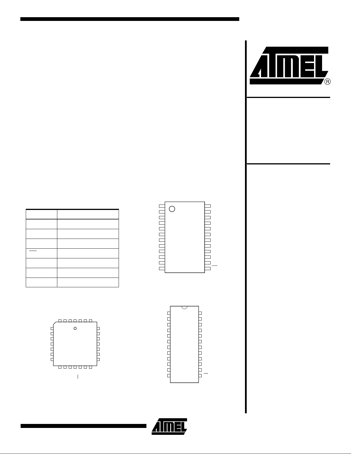
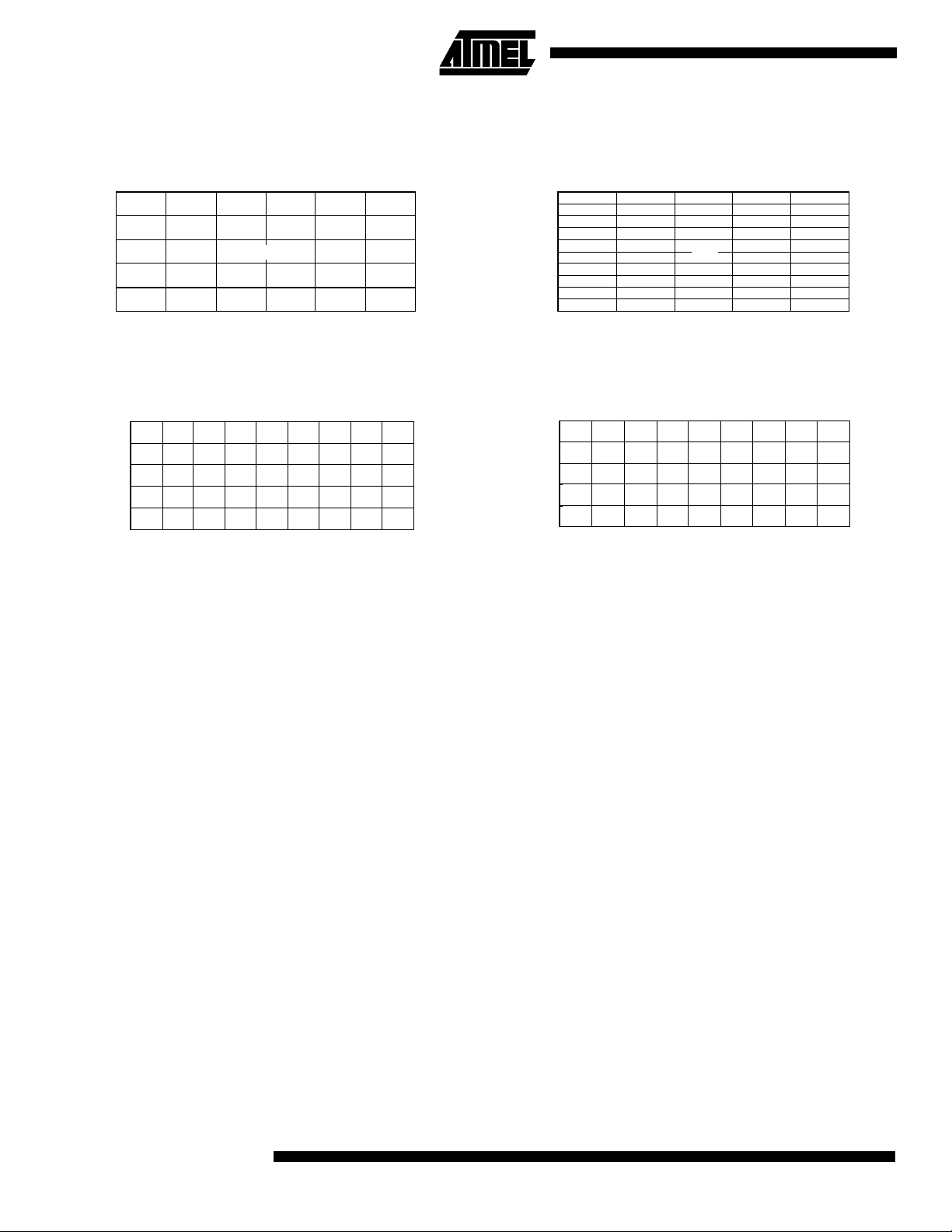
Pin Configurations
All Pinouts Top View
Pin Name Function
CLK Clock
IN Logic Inputs
I/O Bi-directional Buffers
OE
NC No Internal Connection
VCC +5V Supply
PD Power-down
(1)
PD/IN
NC
5
6
IN
7
IN
8
9
IN
10
IN
11
IN
Output Enable
PLCC
ININCLK/INNCVCCINI/O
432
1
282726
12131415161718
IN
IN
GND
NC
IN
OE/IN
25
24
23
22
21
20
19
I/O
I/O
I/O
I/O
NC
I/O
I/O
I/O
CLK/IN
(1)
PD/
GND
IN
IN
IN
IN
IN
IN
IN
IN
IN
IN
CLK/IN
(1)
PD/IN
GND
1
2
3
4
5
6
7
8
9
10
11
12
DIP/SOIC
1
2
IN
3
IN
4
5
IN
6
IN
7
IN
8
IN
9
IN
10
IN
11
IN
12
TSSOP
ATF20V8CQ
VCC
24
IN
23
I/O
22
I/O
21
I/O
20
I/O
19
I/O
18
I/O
17
I/O
16
I/O
15
IN
14
OE/IN
13
24
VCC
23
IN
22
I/O
21
I/O
20
I/O
19
I/O
18
I/O
17
I/O
16
I/O
15
I/O
14
IN
13
OE/IN
ATF20V8CQZ
Note: 1. PD on C and CQ only.
Rev. 0408H–04/01
1
Page 2
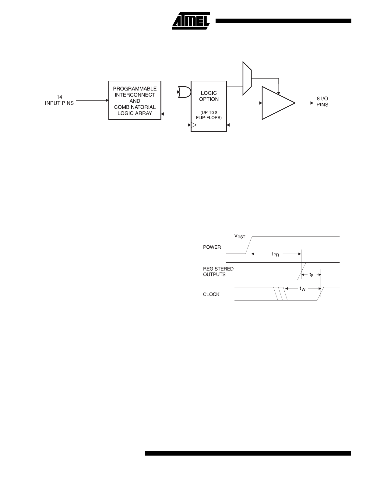
Block Diagram
Description
The ATF20V8C is a high-performance CMOS (electrically
erasable) programmable logic device (PLD) that utilizes
Atmel’s proven electrically erasable technology. Speeds
down to 5 ns and power dissipation as low as 10 µA are
offered. All speed ranges are specified over the full 5V ±
10% range for industrial temperature ranges, and 5V ± 5%
for commercial ranges.
The ATF20V8C(Q) provides a high-speed CMOS PLD
solution with maximum pin-to-pin delay of 5 ns. The
ATF20V8C(Q) also has a user-controlled power-down feature, offering “zero” standby power (10 µA typical). The
user-controlled power-down feature allows the user to
manage total system power to meet specific application
requirements and enhance reliability without sacrificing
speed.
The ATF20V8CQZ provides the zero power CMOS PLD
solution, with “zero” standby power (10 µA typical). The
device powers down automatically through Atmel’s patented Input Transition Detection (ITD) circuitry to the “zero”
standby power mode when all inputs are idle.
Pin “keeper” circuits on input and output pins reduce static
power consumed by pull-ups.
The ATF20V8C(Q)(Z) is the industry-standard 20V8 architecture. Eight outputs are each allocated eight product
terms. Three different modes of operation, configured automatically with software, allow highly complex logic
functions to be realized.
Power-up Reset
uncertainty of how V
lowing conditions are required:
1. The V
2. After reset occurs, all input and feedback setup
times must be met before driving the clock pin high,
and
3. The clock must remain stable during t
rise must be monotonic,
CC
actually rises in the system, the fol-
CC
.
PR
Preload of Registered Outputs
The ATF20V8C registers are provided with circuitry to
allow loading of each register with either a high or a low.
This feature will simplify testing since any state can be
forced into the registers to control test sequencing. A
JEDEC file with preload is generated when a source file
with vectors is compiled. Once downloaded, the JEDEC file
preload sequence will be done automatically by most of the
approved programmers after the programming.
The registers in the ATF20V8Cs are designed to reset during power-up. At a point delayed slightly from V
, all registers will be reset to the low state. As a result,
V
RST
the registered output state will always be high on power-up.
This feature is critical for state machine initialization. However, due to the asynchronous nature of reset and the
2
ATF20V8C Family
crossing
CC
Electronic Signature Word
There are 64 bits of programmable memory that are always
available to the user, even if the device is secured. These
bits can be used for user-specific data.
0408H–04/01
Page 3
ATF20V8C Family
Security Fuse Usage
A single fuse is provided to prevent unauthorized copying
of the ATF20V8C’s fuse patterns. Once programmed, fuse
verify and preload are inhibited. However, the 64-bit User
Signature remains accessible.
The security fuse should be programmed last, as its effect
is immediate.
Programming/Erasing
Programming/erasing is performed using standard PLD
programmers. For further information, see the Configurable
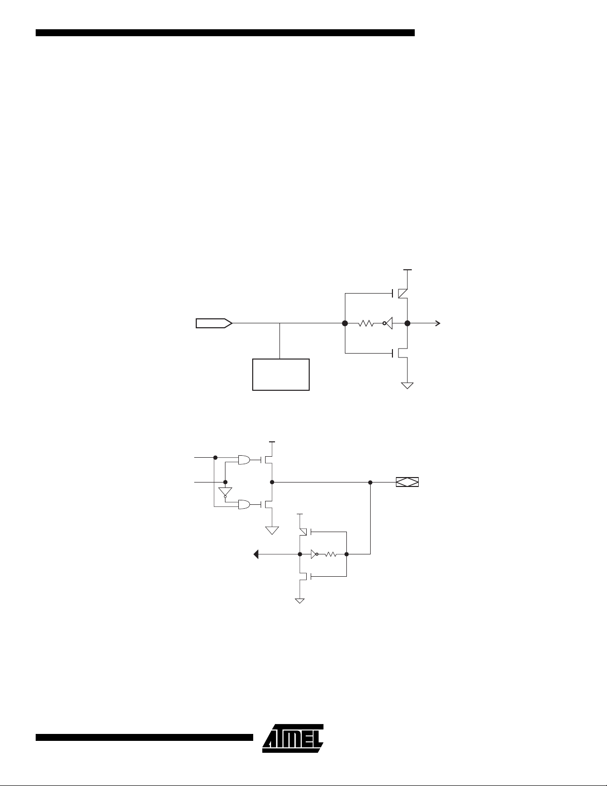
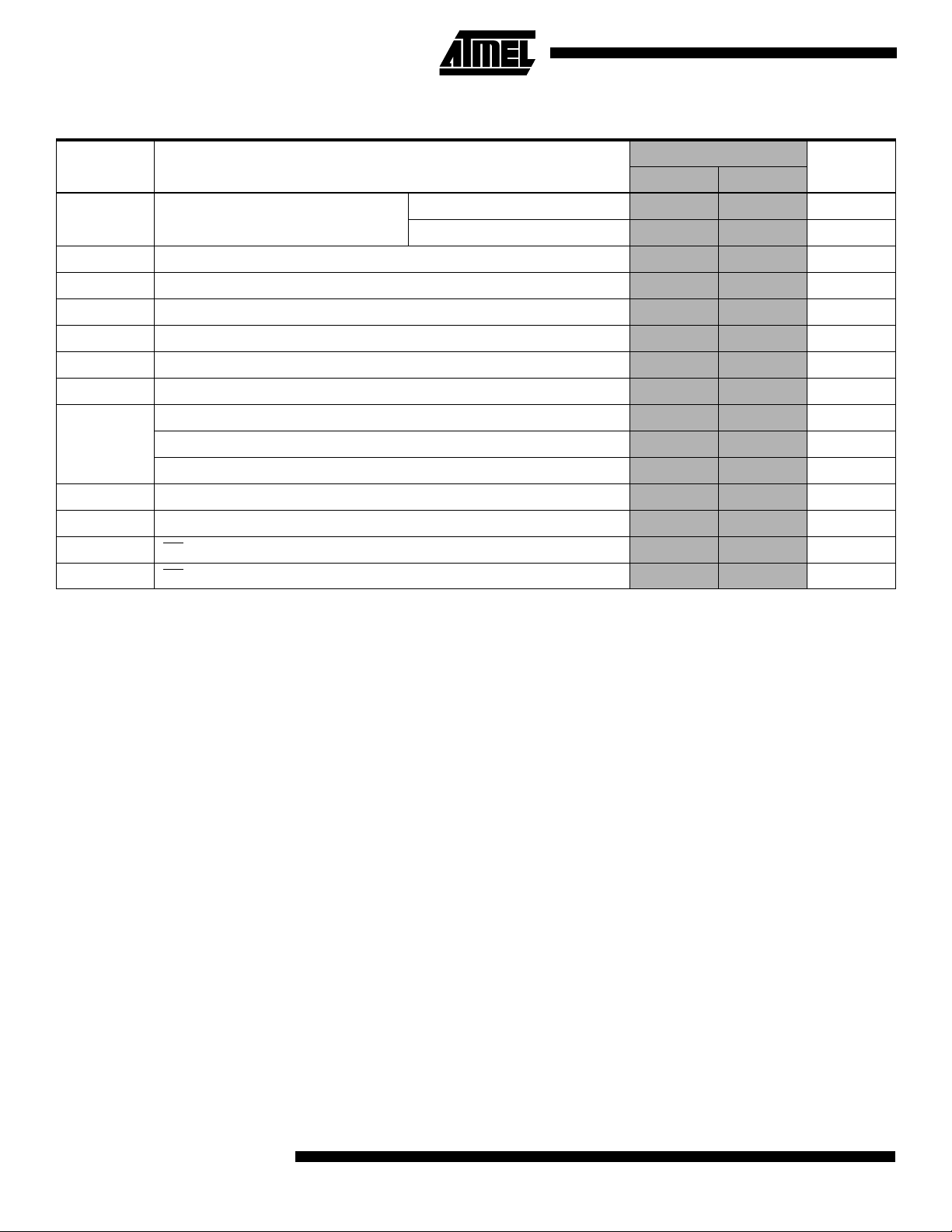
Input Diagram
INPUT
Logic data book section titled, “CMOS PLD Programming
Hardware and Software Support.”
Input and I/O Pull-ups
All ATF20V8C family members have internal input and I/O
“pin-keeper” circuits. Therefore, whenever inputs or I/Os
are not being driven externally, they will maintain their last
driven state. This ensures that all logic array inputs and
device outputs are at known states. These are relatively
weak active circuits that can be easily overridden by TTLcompatible drivers (see input and I/O diagrams below).
V
CC
100K
I/O Diagram
OE
DATA
INPUT
ESD
PROTECTION
CIRCUIT
V
CC
V
CC
I/O
100K
0408H–04/01
3
Page 4

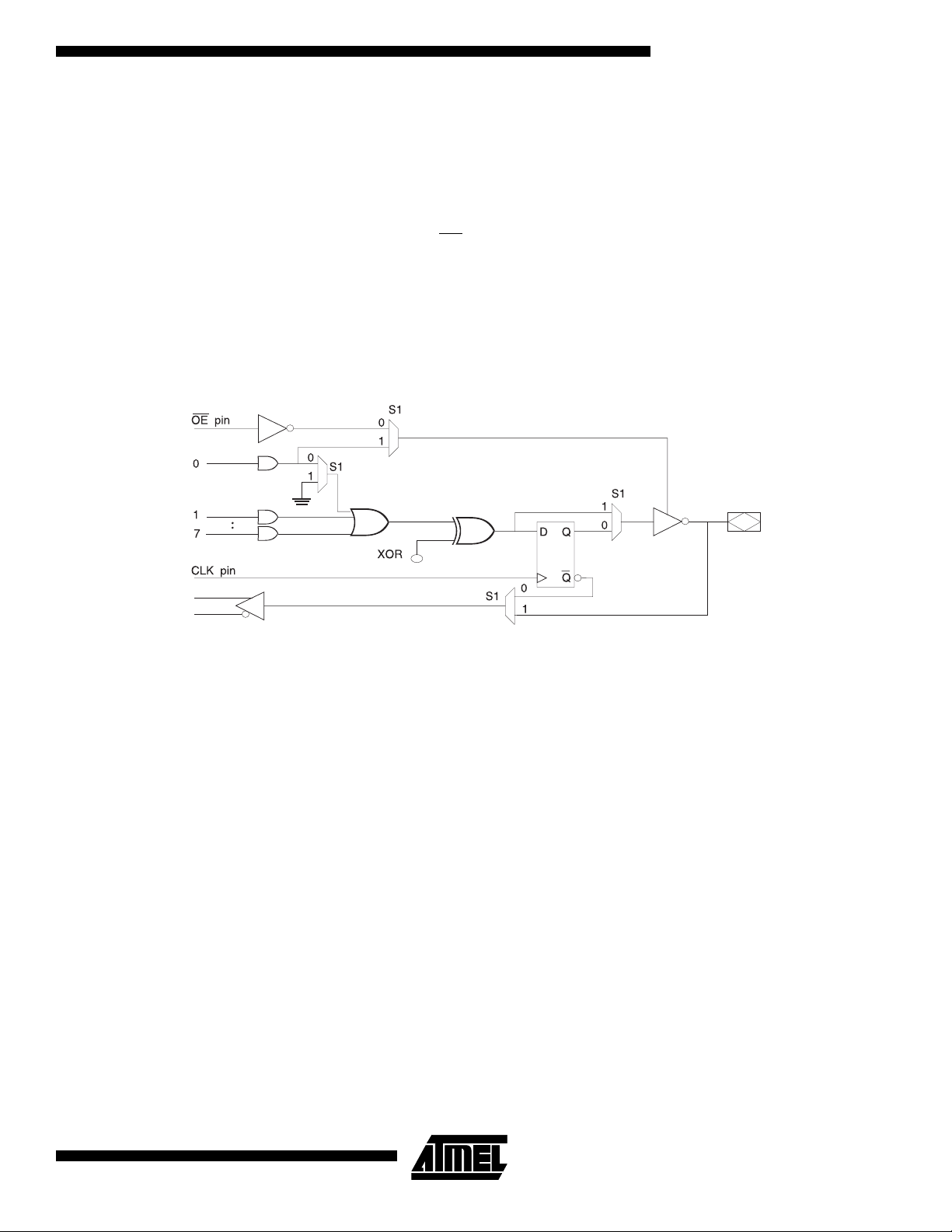
Functional Logic Diagram Description
The logic option and functional diagrams describe the
ATF20V8C architecture. Eight configurable macrocells can
be configured as a registered output, combinatorial I/O,
combinatorial output or dedicated input.
The ATF20V8C’s macrocell can be configured in one of
three different modes. Each mode makes the ATF20V8Cs
look like a different device. The ATF20V8Cs can be a registered output, combinatorial I/O, combinatorial output or
dedicated input. Most PLD compilers can choose the right
mode automatically. The user can also force the selection
by supplying the compiler with a mode selection. The determining factors would be the usage of register versus
combinatorial outputs and dedicated outputs versus output
with output enable control.
The ATF20V8Cs have a user-controlled power-down pin,
which, when active, allows the user to place the device into
operate at high speed. Maximum pin-to-pin delays of 5 ns
are offered. Static power loss due to pull-up resistors is
eliminated by using input and output pin “keeper” circuits
that hold pins to their previous logic levels when idle.
The universal architecture of the ATF20V8Cs can be programmed to emulate many 24-pin PAL devices. The user
can download the subset device JEDEC programming file
to the PLD programmer and the ATF20V8Cs can be configured to act like the chosen device.
Unused product terms are automatically disabled by the
compiler to decrease power consumption. A security fuse,
when programmed, protects the contents the ATF20V8Cs.
Eight bytes (64 fuses) of User Signature are accessible to
the user for purposes such as storing project name, part
number, revision or date. The User Signature is accessible
regardless of the state of the security fuse.
a “zero” standby power-down mode. The device can also
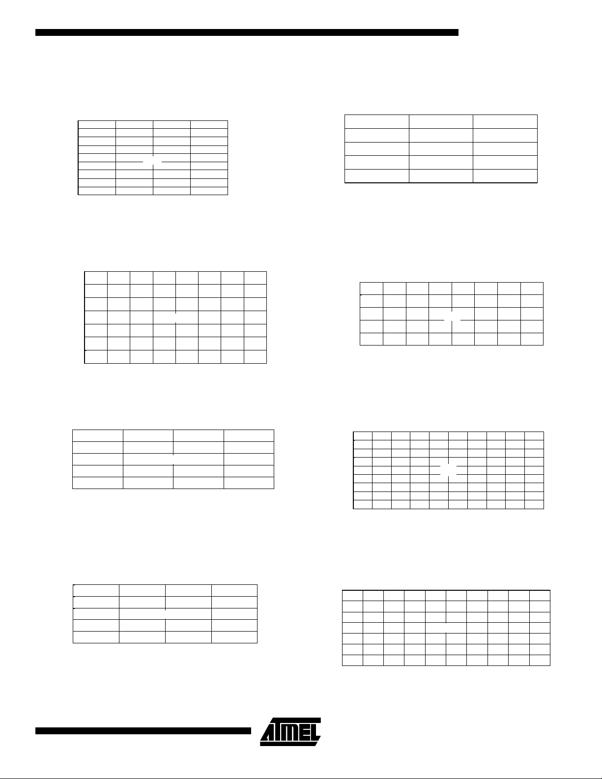
Compiler Mode Selection
Registered Complex Simple Auto Select
ABEL, Atmel-ABEL P20V8R P20V8C P20V8 P20V8
CUPL G20V8MS G20V8MA G20V8 G20V8A
LOG/iC GAL20V8_R
(1)
GAL20V8_C7
(1)
GAL20V8_C8
(1)
GAL20V8
OrCAD-PLD “Registered”“Complex”“Simple” GAL20V8
PLDesigner P20V8 P20V8 P20V8 P20V8
Tango-PLD G20V8 G20V8 G20V8 G20V8
Note: 1. Only applicable for version 3.4 or lower.
4
ATF20V8C Family
0408H–04/01
Page 5
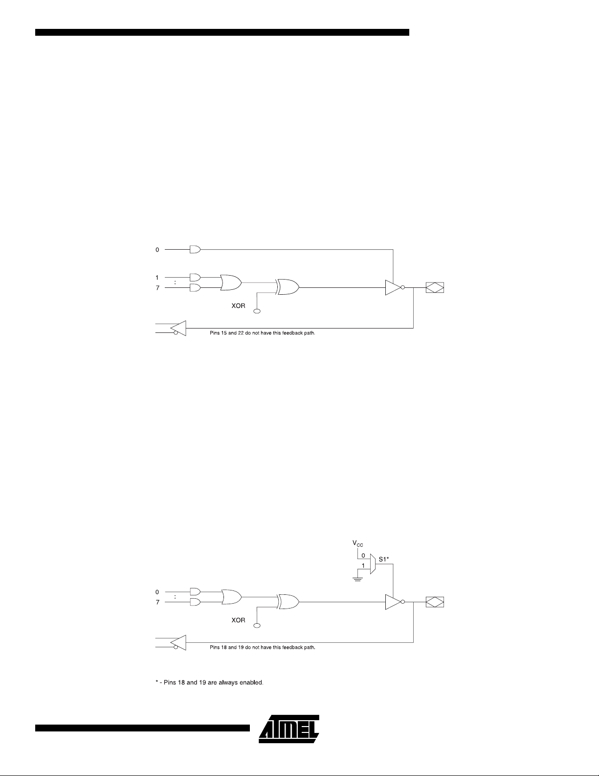
Registered Mode
PAL Device Emulation/PAL Replacement
The registered mode is used if one or more registers are
required. Each macrocell can be configured as either a registered or combinatorial output or I/O, or as an input. For a
registered output or I/O, the output is enabled by the OE
pin, and the register is clocked by the CLK pin. Eight product terms are allocated to the sum term. For a combinatorial output or I/O, the output enable is controlled by a
product term, and seven product terms are allocated to the
Registered Mode Operation
ATF20V8C Family
sum term. When the macrocell is configured as an input,
the output enable is permanently disabled.
Any register usage will make the compiler select this mode.
The following registered devices can be emulated using
this mode:
20R8 20RP8
20R6 20RP6
20R4 20RP4
0408H–04/01
5
Page 6

Registered Mode Logic Diagram
6
ATF20V8C Family
0408H–04/01
Page 7
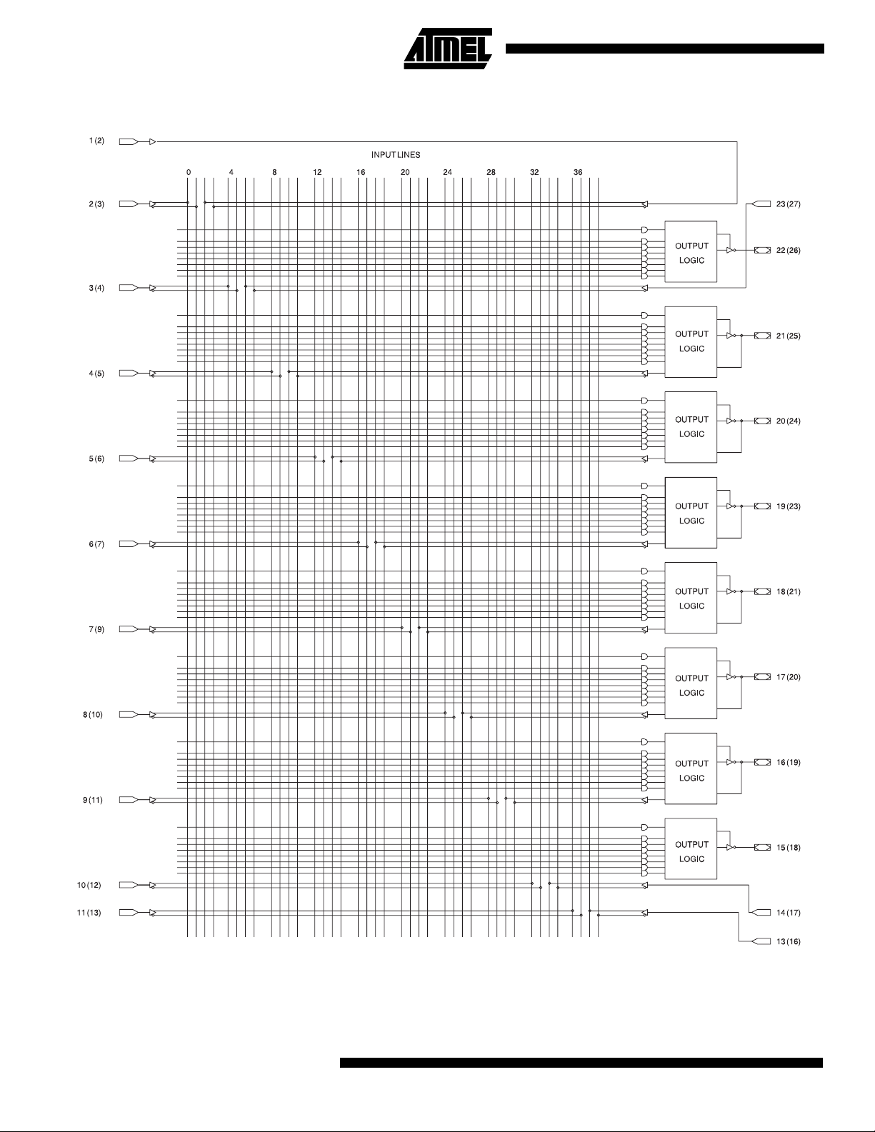
Complex Mode
PAL Device Emulation/PAL Replacement
In the Complex Mode, combinatorial output and I/O functions are possible. Pins 1 and 11 are regular inputs to the
array. Pins 13 through 18 have pin feedback paths back to
the AND-array, which makes full I/O capability possible.
Pins 12 and 19 (outermost macrocells) are outputs only.
They do not have input capability. In this mode, each
macrocell has seven product terms going to the sum term
and one product term enabling the output.
Complex Mode Operation
ATF20V8C Family
Combinatorial applications with an OE requirement will
make the compiler select this mode. The following devices
can be emulated using this mode:
20L8
20H8
20P8
Simple Mode
PAL Device Emulation/PAL Replacement
In the Simple Mode, eight product terms are allocated to
the sum term. Pins 15 and 16 (center macrocells) are permanently configured as combinatorial outputs. Other macrocells can be either inputs or combinatorial outputs with
pin feedback to the AND-array. Pins 1 and 11 are regular
inputs.
Simple Mode Option
The compiler selects this mode when all outputs are combinatorial without OE control. The following simple PALs can
be emulated using this mode:
14L8 14H8 14P8
16L6 18H6 16P6
18L4 18H4 18P4
20L2 20H2 20P2
0408H–04/01
7
Page 8
Complex Mode Logic Diagram
8
ATF20V8C Family
0408H–04/01
Page 9
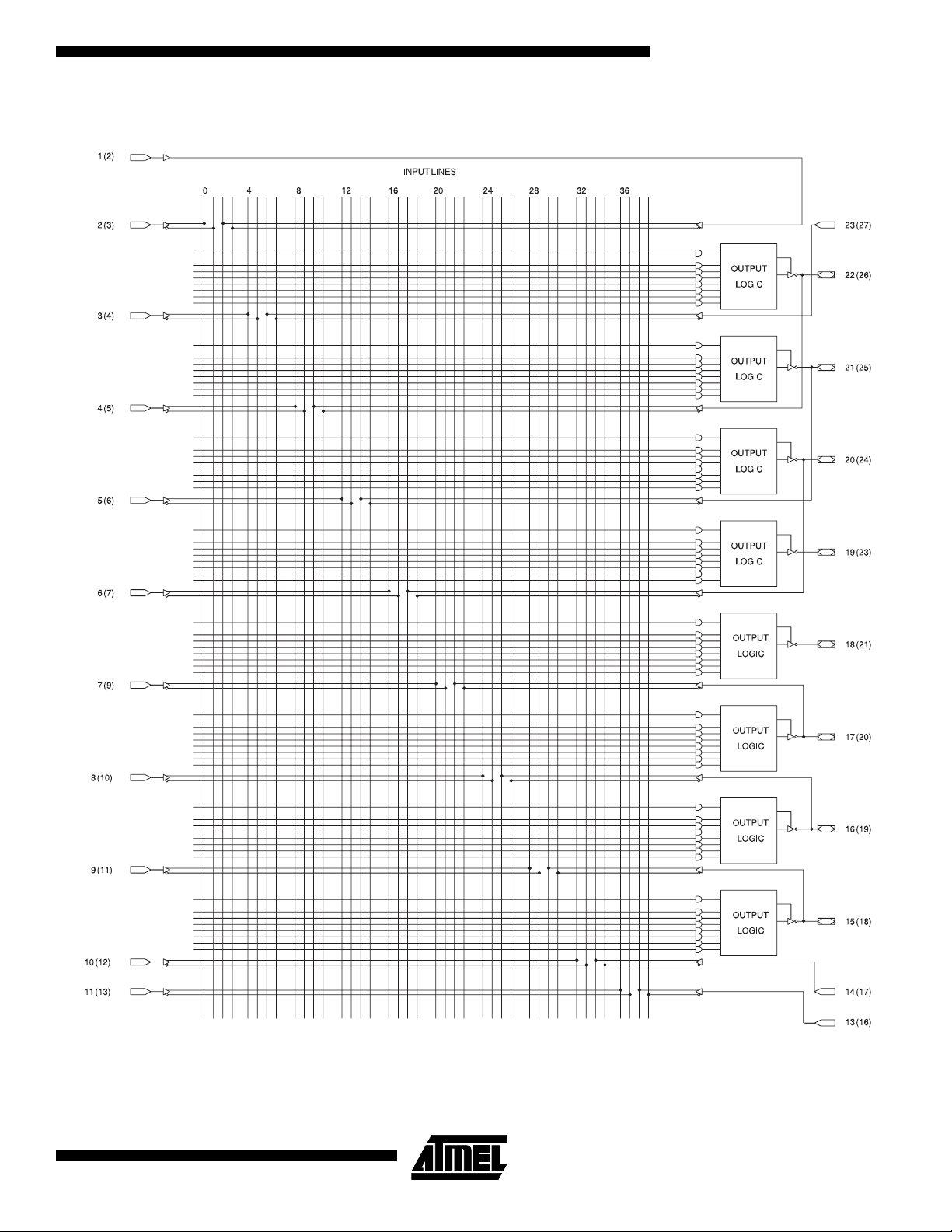
Simple Mode Logic Diagram
ATF20V8C Family
0408H–04/01
9
Page 10

Absolute Maximum Ratings*
Temperature under Bias ................................ -55°C to +125°C
Storage Temperature..................................... -65°C to +150°C
Voltage on Any Pin with
Respect to Ground .........................................-2.0V to +7.0V
Voltage on Input Pins
with Respect to Ground
during Programming .....................................-2.0V to +14.0V
Programming Voltage with
Respect to Ground .......................................-2.0V to +14.0V
(1)
(1)
(1)
*NOTICE: Stresses beyond those listed under “Absolute
Maximum Ratings” may cause permanent damage to the device. This is a stress rating only and
functional operation of the device at these or any
other conditions beyond those indicated in the
operational sections of this specification is not
implied. Exposure to absolute maximum rating
conditions for extended periods may affect device
reliability.
Note: 1. Minimum voltage is -0.6V DC, which may under-
shoot to -2.0V for pulses of less than 20 ns. Maximum output pin voltage is V
+ 0.75V DC, which
CC
may overshoot to 7.0V for pulses of less than
20 ns.
DC and AC Operating Conditions
Commercial Industrial
Operating Temperature (Ambient) 0°C - 70°C-40°C - 85°C
V
Power Supply 5V=± 5% 5V=± 10%
CC
Parameter Description Typ Max Units
t
PR
V
RST
Power-up Reset Time 600 1,000 ns
Power-up Reset Voltage 3.8 4.5 V
10
ATF20V8C Family
0408H–04/01
Page 11

ATF20V8C Family
Input Test Waveforms and
Output Test Loads
Measurement Levels
Commercial
tR, tF < 1.5 ns (10% to 90%)
Pin Capacitance
f = 1 MHz, T = 25°C
C
IN
C
OUT
Note: 1. Typical values for nominal supply voltage. This parameter is only sampled and is not 100% tested.
(1)
Typ Max Units Conditions
58 pF V
68 pF V
IN
OUT
= 0V
= 0V
0408H–04/01
11
Page 12

ATF20V8C DC Characteristics
VCC = 5.0V and TA = 25°C
Symbol Parameter Condition Min Typ Max Units
I
I
I
I
IL
IH
CC
CC2
Input or I/O Low
Leakage Current
Input or I/O High
Leakage Current
Power Su ppl y
Current, Standby
Clocked Power
Supply Current
0 ≤=VIN ≤=VIL (Max) -35 -100 µA
3.5 ≤=VIN ≤=V
CC
10 µA
C-5 Com. 60 90 mA
C-5 Ind. 60 100 mA
C-7 Com. 60 90 mA
V
= Max,
CC
V
= Max,
IN
Outputs Open
C-7 Ind. 60 100 mA
C-10 Com. 60 80 mA
C-10 Ind. 60 90 mA
C-15 Com. 60 80 mA
C-15 Ind. 60 90 mA
C-5 Com. 70 110 mA
C-5 Ind. 70 125 mA
C-7 Com. 70 110 mA
= Max,
V
CC
C-7 Ind. 70 125 mA
Outputs Open,
f = 15 MHz
C-10 Com. 60 90 mA
C-10 Ind. 60 105 mA
C-15 Com. 60 90 mA
C-15 Ind. 60 105 mA
(1)
IOS
Output Short
V
= 0.5V -130 mA
OUT
Circuit Current
V
IL
V
IH
V
OL
V
OH
Input Low Voltage -0.5 0.8 V
Input High Voltage 2.0 VCC + 0.75 V
= VIH or VIL,
V
Output Low Voltage
V
IN
CC
= Min
Output High Voltage VIN = VIH or VIL,
= Min
V
CC
IOL = 24 mA
= 16 mA 0.5 V
I
OL
I
= -4.0 mA 2.4 V
OH
Com.,
Ind.
0.5 V
Notes: 1. Not more than one output at a time should be shorted. Duration of short circuit test should not exceed 30 sec.
2. All values are at V
and TA=25°C.
CC
3. Shaded area indicates preliminary data.
12
ATF20V8C
0408H–04/01
Page 13

ATF20V8C
AC Waveforms
(1)
Note: 1. Timing measurement reference is 1.5V. Input AC driving levels are 0.0V and 3.0V, unless otherwise specified.
ATF20V8C Family AC Characteristics
(1)
C-5 C-7 C-10 C-15
Symbol Parameter
t
PD
Input or Feedback to
Non-registered Output
8 outputs switching
1 output switching 7 10 ns
Min Max Min Max Min Max Min Max
3 5 3 7.5 3 10 3 15 ns
Units
t
CF
t
CO
t
S
t
H
t
P
t
W
Clock to Feedback 3 3 68ns
Clock to Output 2 4 2 5 2 7 2 10 ns
Input or Feedback Setup Time 3 5 7.5 12 ns
Hold Time 0 0 0 0ns
Clock Period 6 8 12 16 ns
Clock Width 3 4 6 8ns
External Feedback 1/(tS + tCO) 143 100 68 45 MHz
f
t
t
t
t
MAX
EA
ER
PZX
PXZ
Internal Feedback 1/(t
No Feedback 1/(t
Input to Output Enable – Product Term 3 6 3 9 3 10 3 15 ns
Input to Output Disable – Product Term 2 6 2 9 2 10 2 15 ns
OE pin to Output Enable 2 5 2 6 2 10 2 15 ns
OE pin to Output Disable 1.5 5 1.5 6 1.5 10 1.5 15 ns
+ tCF) 167 125 74 50 MHz
S
) 7 167 125 83 62 MHz
P
Notes: 1. See ordering information for valid part numbers and speed grades.
2. Shaded area indicates preliminary data.
0408H–04/01
13
Page 14

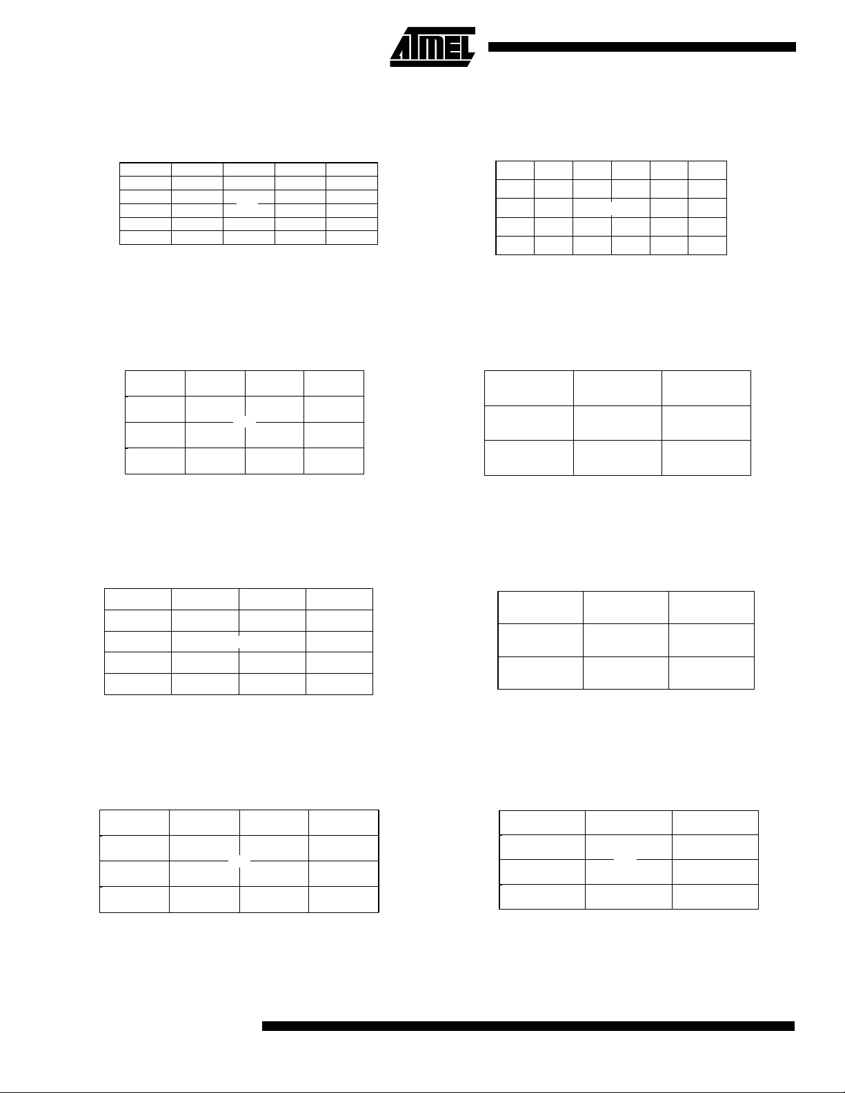
ATF20V8C Characteristic Curves
STAND-BY ICC VS.
4.5
SUPPLY VOLTAGE (T
4.0
3.5
3.0
2.5
(µA)
CC
I
2.0
1.5
TBD
1.0
0.5
0.0
4.5 4.8 5.0 5.3 5.5
SUPPLY VOLTAGE (V)
= 25°C)
A
SUPPLY CURRENT VS.
140.000
120.000
100.000
80.000
(mA)
60.000
CC
I
40.000
20.000
0.000
INPUT FREQUENCY (V
0.0 0. 5 2.5 5. 0 7.5 10.0 25.0 37.5 50.0
FRE QUE NCY (M Hz )
= 5.0V, TA = 25°C)
CC
TBD
NORMALIZED ICC VS. TEMP
1.4
1.2
1.0
0.8
0.6
NORMALIZED Icc
0.4
-40.0 0.0 25.0 75.0
TBD
TEM PERAT URE (C)
SUPPLY CURRENT VS.
1.000
0.800
0.600
(mA)
0.400
CC
I
0.200
0.000
INPUT FREQUENCY (V
0.0 0. 5 2.5 5.0 7.5 10. 0 25.0 37.5 50. 0
FRE QUE NCY (M Hz )
= 5.0V, TA = 25°C)
CC
TBD
OUTPUT SOURCE CURRENT VS.
0
-10
-20
(mA)
-30
OH
I
-40
-50
4.0 4.5 5.0 5.5 6.0
SUPPLY VOLTAGE (V
TBD
SUPPLY VOLTAGE (V)
= 2.4V)
OH
OUTPUT SINK CURRENT VS.
1
1
1
0
Iol (mA)
0
0
4.04.55.05.56.0
SUPPLY VOLTAGE (V
TBD
SUPPLY VOLTAGE (V)
= 0.5V)
OL
OUTPUT SOURCE CURRENT VS.
0.0
-10.0
-20.0
-30.0
-40.0
(mA)
-50.0
OH
I
-60.0
-70.0
-80.0
-90.0
OUTPUT VOLTAGE (V
0.00 0.50 1. 00 1.50 2.00 2.50 3.00 3.50 4. 00 4.50 5.0 0
= 5.0V , TA = 25°C)
CC
TBD
V
(V)
OH
OUTPUT SINK CURRENT VS.
140.0
120.0
100.0
80.0
(mA)
60.0
OL
I
40.0
20.0
0.0
0.0 0.5 1.0 1.5 2.0 2.5 3.0 3.5 4.0 4.5 5.0
OUTPUT VOLTAGE (V
SUPPLY VOLTAGE (V)
= 5.0V, TA = 25°C)
CC
TBD
14
ATF20V8C
0408H–04/01
Page 15
ATF20V8C Characteristic Curves (Continued)
T
ATF20V8C
INPUT CLAMP CURRENT VS.
INPUT VOLTAGE (V
0
-20
-40
-60
(mA)
-80
-100
INPUT CURREN
-120
0.0 -0.2 -0.4 -0.6 -0.8 -1.0
1.2
PD
1.1
1.0
0.9
NORMALIZED T
0.8
4.5 4.8 5.0 5.3 5.5
INPUT VOLTAGE (V)
NORMALIZED TPD VS. VCC
SUPPLY VOLTAGE (V)
= 5.0V, TA = 35°C)
CC
TBD
TBD
INPUT CURRENT VS.
INPUT VOLTAGE (VCC = 5.0V , TA = 25°C)
1
1
1
(uA)
0
0
INPUT CURRENT
0
0.0 1.0 2. 0 3. 0 4.0 5. 0 6.0
1.1
PD
1.0
0.9
NORMALIZED T
0.8
-40.0 0.0 25.0 75.0
NORMALIZED TPD VS. TEMP
TBD
INPUT VOLTAGE (V)
TBD
TEMPERATURE (C)
1.3
CO
1.2
1.1
1.0
0.9
NORMALIZED T
0.8
4.5 4.8 5.0 5.3 5.5
NORMALIZED TCO VS. VCC
TBD
SUPPLY VOLTAGE (V)
NORMALIZED TSU VS. VCC
1.2
SU
1.1
1.0
0.9
NORMALIZED T
0.8
4.5 4.8 5.0 5.3 5.5
SUPPLY VOLTAGE (V)
TBD
1.1
CO
1.0
TBD
0.9
NORMALIZED T
0.8
-40.0 0.0 25.0 75.0
TEM P ERAT URE (V )
NORMALIZED TSU VS. TEMP
1.2
CO
1.1
NORMALIZED TCO VS. TEMP
1.0
0.9
NORMALIZED T
0.8
-40.0 0.0 25.0 75.0
TBD
TEMP ERATURE (C)
15
0408H–04/01
Page 16
ATF20V8C Characteristic Curves (Continued)
DELTA TPD VS.
8
6
(ns)
4
PD
2
DELTA T
0
-2
0 50 100 150 200 250 300
OUTPUT LOADING
TBD
OUTPUT LOADING (PF)
DELTA TPD VS. # OF OUTPUT SWITC HING
0.0
-0.1
(ns)
-0.2
PD
-0.3
-0.4
DELTA T
-0.5
1.0 2.0 3.0 4.0 5.0 6.0 7.0 8.0 9.0 10.0
NUMBER OF OUTPUTS SWITCHING
TBD
DELTA TCO VS.
1.00
0.90
0.80
0.70
(ns)
0.60
CO
0.50
0.40
0.30
0.20
DELTA T
0.10
0.00
50 100 150 200 25 0 300
OUTPUT LOADING
TBD
NUMBER OF OUTPUTS LOADING
DELTA TCO VS. # OF OUTPUT SWITCHING
1.0
0.8
(ns)
0.6
CO
0.4
0.2
DELTA T
0.0
1.02.03.04.05.06.07.08.09.010.0
NUMBER OF OUTPUTS SWITCHING
TBD
16
ATF20V8C
0408H–04/01
Page 17
ATF20V8CQ
ATF20V8CQ DC Characteristics
VCC = 5.0V and TA = 25°C
Symbol Parameter Condition Min Typ Max Units
I
IL
Input or I/O Low
0 ≤=VIN ≤=VIL (Max) -35 -100 µA
Leakage Current
I
IH
Input or I/O High
3.5 ≤=VIN ≤=V
CC
10 µA
Leakage Current
I
CC
Power Su ppl y
Current, Standby
VCC = Max,
V
= Max,
IN
CQ-10, -15 Com. 10 25 µA
Outputs Open
I
CC2
Clocked Power
Supply Current
VCC = Max,
Outputs Open,
CQ-10, 15 Com. 40 55 mA
f = 15 MHz
(1)
IOS
Output Short
V
= 0.5V -130 mA
OUT
Circuit Current
V
IL
V
IH
V
OL
V
OH
Input Low Voltage -0.5 0.8 V
Input High Voltage 2.0 VCC + 0.75 V
Com.,
Ind.
0.5 V
Output Low Voltage
Output High Voltage
= VIH or VIL,
V
IN
= Min
V
CC
= VIH or VIL,
V
IN
= Min
V
CC
IOL = 24 mA
= 16 mA 0.5 V
I
OL
= -4.0 mA 2.4 V
I
OH
Notes: 1. Not more than one output at a time should be shorted. Duration of short circuit test should not exceed 30 sec.
2. Shaded areas indicate preliminary data.
0408H–04/01
17
Page 18
ATF20V8CQ AC Characteristics
(1)
CQ-10
Symbol Parameter
t
PD
t
CF
t
CO
t
S
t
H
t
P
t
W
Input or Feedback to
Non-registered Output
Clock to Feedback 6ns
Clock to Output 2 7ns
Input or Feedback Setup Time 7.5 ns
Hold Time 0 ns
Clock Period 12 ns
Clock Width 6 ns
8 outputs switching
1 output switching
External Feedback 1/(tS + tCO) 68 MHz
f
t
t
t
t
MAX
EA
ER
PZX
PXZ
Internal Feedback 1/(tS + tCF) 74 MHz
No Feedback 1/(t
) 83 MHz
P
Input to Output Enable – Product Term 3 10 ns
Input to Output Disable – Product Term 2 10 ns
OE pin to Output Enable 2 10 ns
OE pin to Output Disable 1.5 10 ns
Notes: 1. See ordering information for valid part numbers and speed grades.
2. All values are at V
=5V and TA=25°C.
CC
3. Shaded areas indicate preliminary data.
Min Max
3 10 ns
Units
ns
18
ATF20V8CQ
0408H–04/01
Page 19
ATF20V8CQ Characteristic Curves
ATF20V8CQ
STAND-BY ICC VS.
4.5
4.0
3.5
3.0
2.5
(µA)
2.0
CC
I
1.5
1.0
0.5
0.0
4.5 4.8 5. 0 5. 3 5. 5
SUPPLY VOLTAGE (T
TBD
SUPPLY VOLTAGE (V)
= 25°C)
A
SUPPLY CURRENT VS.
140.000
120.000
100.000
80.000
(mA)
60.000
CC
I
40.000
20.000
0.000
INPUT FREQUENCY (V
0.0 0. 5 2.5 5. 0 7.5 10.0 25.0 37.5 50.0
FRE QUE NCY (M Hz )
= 5.0V, TA = 25°C)
CC
TBD
NORMALIZED ICC VS. TEMP
1.4
1.2
1.0
0.8
0.6
NORMALIZED Icc
0.4
-40.0 0.0 25.0 75.0
TBD
TEM PERAT URE (C)
SUPPLY CURRENT VS.
1.000
0.800
0.600
(mA)
0.400
CC
I
0.200
0.000
INPUT FREQUENCY (V
0.0 0. 5 2.5 5.0 7.5 10. 0 25.0 37.5 50. 0
FRE QUE NCY (M Hz )
= 5.0V, TA = 25°C)
CC
TBD
OUTPUT SOURCE CURRENT VS.
0
SUPPLY VOLTAGE (V
-10
-20
(mA)
-30
OH
I
-40
TBD
-50
4.04.55.05.56.0
SUPPLY VOLTAGE (V)
= 2.4V )
OH
OUTPUT SINK CURRENT VS.
1
1
1
0
Iol (mA)
0
0
4.04.55.05.56.0
SUPPLY VOLTAGE (V
TBD
SUPPLY VOLTAGE (V)
= 0.5V)
OL
OUTPUT SOURCE CURRENT VS.
0.0
-10.0
-20.0
-30.0
-40.0
(mA)
-50.0
OH
I
-60.0
-70.0
-80.0
-90.0
OUTPUT VOLTAGE (V
0.00 0.50 1. 00 1.50 2. 00 2.50 3.00 3.50 4. 00 4.50 5.00
= 5.0V , TA = 25°C)
CC
TBD
(V)
V
OH
OUTPUT SINK CURRENT VS.
140.0
120.0
100.0
80.0
(mA)
60.0
OL
I
40.0
20.0
0.0
0.0 0.5 1.0 1.5 2.0 2.5 3.0 3.5 4.0 4.5 5.0
OUTPUT VOLTAGE (V
SUPPLY VOLTAGE (V)
= 5.0V, TA = 25°C)
CC
TBD
0408H–04/01
19
Page 20
ATF20V8CQ Characteristic Curves (Continued)
INPUT CLAMP CURRENT VS.
INPUT VOLTAGE (V
0
-20
-40
-60
INPUT
-80
-100
CURRENT (mA)
-120
0.0 -0.2 -0.4 -0.6 -0.8 -1.0
1.2
PD
1.1
1.0
0.9
NORMALIZED T
0.8
4.5 4.8 5.0 5.3 5.5
INPUT VOLTAGE (V)
NORMALIZED TPD VS. VCC
SUPPLY VOLTAGE (V)
= 5.0V, TA = 35°C)
CC
TBD
TBD
INPUT CURRENT VS.
INPUT VOLTAGE (VCC = 5.0V , TA = 25°C)
1
1
1
(uA)
0
0
INPUT CURRENT
0
0.0 1.0 2. 0 3. 0 4.0 5. 0 6.0
1.1
PD
1.0
0.9
NORMALIZED T
0.8
-40.0 0.0 25.0 75.0
NORMALIZED TPD VS. TEMP
TBD
INPUT VOLTAGE (V)
TBD
TEMPERATURE (C)
1.3
CO
1.2
1.1
1.0
0.9
NORMALIZED T
0.8
4.5 4.8 5.0 5.3 5.5
NORMALIZED TCO VS. VCC
TBD
SUPPLY VOLTAGE (V)
NORMALIZED TSU VS. VCC
1.2
SU
1.1
1.0
0.9
NORMALIZED T
0.8
4.5 4.8 5.0 5.3 5.5
SUPPLY VOLTAGE (V)
TBD
1.1
CO
1.0
TBD
0.9
NORMALIZED T
0.8
-40.0 0.0 25.0 75.0
TEM P ERAT URE (V )
NORMALIZED TSU VS. TEMP
1.2
CO
1.1
NORMALIZED TCO VS. TEMP
1.0
0.9
NORMALIZED T
0.8
-40.0 0.0 25.0 75.0
TBD
TEMP ERATURE (C)
20
ATF20V8CQ
0408H–04/01
Page 21
ATF20V8CQ Characteristic Curves (Continued)
ATF20V8CQ
DELTA TPD VS.
8
6
(ns)
4
PD
2
DELTA T
0
-2
0 50 100 150 200 250 300
OUTPUT LOADING
TBD
OUTPUT LOADING (PF)
DELTA TPD VS. # OF OUTPUT SWITC HING
0.0
-0.1
(ns)
-0.2
PD
-0.3
-0.4
DELTA T
-0.5
1.0 2.0 3.0 4.0 5.0 6.0 7.0 8.0 9.0 10.0
NUMBER OF OUTPUTS SWITCHING
TBD
DELTA TCO VS.
1.00
0.90
0.80
0.70
(ns)
0.60
CO
0.50
0.40
0.30
0.20
DELTA T
0.10
0.00
50 100 150 200 25 0 300
OUTPUT LOADING
TBD
NUMBER OF OUTPUTS LOADING
DELTA TCO VS. # OF OUTPUT SWITCHING
1.0
0.8
(ns)
0.6
CO
0.4
0.2
DELTA T
0.0
1.02.03.04.05.06.07.08.09.010.0
NUMBER OF OUTPUTS SWITCHING
TBD
0408H–04/01
21
Page 22
ATF20V8CQZ DC Characteristics
VCC = 5.0V and TA = 25°C
Symbol Parameter Condition Min Typ Max Units
I
IL
Input or I/O Low
0 ≤=VIN ≤=VIL (Max) -35 -100 µA
Leakage Current
I
IH
Input or I/O High
3.5 ≤=VIN ≤=V
CC
10 µA
Leakage Current
V
I
CC
I
CC2
IOS
Power Su ppl y
Current, Standby
Clocked Power
Supply Current
(1)
Output Short
= Max,
CC
V
= Max,
IN
CQZ-15
Outputs Open
VCC = Max,
Outputs Open,
CQZ-15
f = 15 MHz
V
= 0.5V -130 mA
OUT
Com. 10 25 µA
Ind. 10 50 µA
Com. 20 35 mA
Ind. 20 40 mA
Circuit Current
V
IL
V
IH
V
OL
V
OH
Input Low Voltage -0.5 0.8 V
Input High Voltage 2.0 VCC + 0.75 V
Com.,
Ind.
0.5 V
Output Low Voltage
Output High Voltage
= VIH or VIL,
V
IN
= Min
V
CC
= VIH or VIL,
V
IN
= Min
V
CC
IOL = 24 mA
= 16 mA 0.5 V
I
OL
= -4.0 mA 2.4 V
I
OH
Notes: 1. Not more than one output at a time should be shorted. Duration of short circuit test should not exceed 30 sec.
2. All values are at V
=5V and TA=25°C.
CC
3. Shaded areas indicate preliminary data.
22
ATF20V8CQZ
0408H–04/01
Page 23

ATF20V8CQZ
ATF20V8CQZ AC Characteristics
(1)
Symbol Parameter
t
PD
t
CF
t
CO
t
S
t
H
t
P
t
W
Input or Feedback to
Non-registered Output
Clock to Feedback 8ns
Clock to Output 2 10 ns
Input or Feedback Setup Time 12 ns
Hold Time 0 ns
Clock Period 16 ns
Clock Width 8 ns
8 outputs switching
1 output switching
External Feedback 1/(tS + tCO) 45 MHz
f
MAX
Internal Feedback 1/(t
+ tCF) 50 MHz
S
No Feedback 1/(tP) 62 MHz
t
t
t
t
EA
ER
PZX
PXZ
Input to Output Enable – Product Term 3 15 ns
Input to Output Disable – Product Term 2 15 ns
OE pin to Output Enable 2 15 ns
OE pin to Output Disable 1.5 15 ns
Notes: 1. See ordering information for valid part numbers and speed grades.
2. Shaded areas indicate preliminary data.
CQZ-15
Min Max
3 15 ns
10 ns
Units
0408H–04/01
23
Page 24
ATF20V8CQZ Characteristic Curves
STAND-BY ICC VS.
4.5
4.0
3.5
3.0
2.5
(µA)
2.0
CC
I
1.5
1.0
0.5
0.0
4.5 4.8 5. 0 5. 3 5. 5
SUPPLY VOLTAGE (T
TBD
SUPPLY VOLTAGE (V)
= 25°C)
A
SUPPLY CURRENT VS.
140.000
120.000
100.000
80.000
(mA)
60.000
CC
I
40.000
20.000
0.000
INPUT FREQUENCY (V
0.0 0. 5 2.5 5. 0 7.5 10.0 25.0 37.5 50.0
FRE QUE NCY (M Hz )
= 5.0V, TA = 25°C)
CC
TBD
NORMALIZED ICC VS. TEMP
1.4
1.2
1.0
0.8
0.6
NORMALIZED Icc
0.4
-40.0 0.0 25.0 75.0
TBD
TEM PERAT URE (C)
SUPPLY CURRENT VS.
1.000
0.800
0.600
(mA)
0.400
CC
I
0.200
0.000
INPUT FREQUENCY (V
0.0 0. 5 2.5 5.0 7.5 10. 0 25.0 37.5 50. 0
FRE QUE NCY (M Hz )
= 5.0V, TA = 25°C)
CC
TBD
OUTPUT SOURCE CURRENT VS.
0
-10
-20
(mA)
-30
OH
I
-40
-50
4.0 4.5 5.0 5.5 6. 0
SUPPLY VOLTAGE (V
TBD
SUPPLY VOLTAGE (V)
= 2.4V)
OH
OUTPUT SINK CURRENT VS.
1
1
1
0
Iol (mA)
0
0
4.04.55.05.56.0
SUPPLY VOLTAGE (V
TBD
SUPPLY VOLTAGE (V)
= 0.5V)
OL
OUTPUT SOURCE CURRENT VS.
0.0
-10.0
-20.0
-30.0
-40.0
(mA)
-50.0
OH
I
-60.0
-70.0
-80.0
-90.0
OUTPUT VOLTAGE (V
0.00 0.50 1. 00 1.50 2.00 2.50 3.00 3.50 4. 00 4.50 5.0 0
= 5.0V , TA = 25°C)
CC
TBD
V
(V)
OH
OUTPUT SINK CURRENT VS.
140.0
120.0
100.0
80.0
(mA)
60.0
OL
I
40.0
20.0
0.0
0.0 0.5 1.0 1.5 2.0 2.5 3.0 3.5 4.0 4.5 5.0
OUTPUT VOLTAGE (V
SUPPLY VOLTAGE (V)
= 5.0V, TA = 25°C)
CC
TBD
24
ATF20V8CQZ
0408H–04/01
Page 25
ATF20V8CQZ-15 Characteristic Curves (Continued)
ATF20V8CQZ
INPUT CLAMP CURRENT VS.
INPUT VOLTAGE (V
0
-20
-40
-60
INPUT
-80
-100
CURRENT (mA)
-120
0.0 -0.2 -0.4 -0.6 -0.8 -1.0
1.2
PD
1.1
1.0
0.9
NORMALIZED T
0.8
4.5 4.8 5.0 5.3 5.5
INPUT VOLTAGE (V)
NORMALIZED TPD VS. VCC
SUPPLY VOLTAGE (V)
= 5.0V, TA = 35°C)
CC
TBD
TBD
INPUT CURRENT VS.
INPUT VOLTAGE (V
1
1
1
(uA)
0
0
INPUT CURRENT
0
0.0 1.0 2.0 3.0 4.0 5.0 6.0
1.1
PD
1.0
0.9
NORMALIZED T
0.8
-40.0 0.0 25.0 75.0
INPUT VOLTAGE (V)
NORMALIZED TPD VS. TEMP
TEMPERATURE (C)
= 5.0V , TA = 25°C)
CC
TBD
TBD
1.3
CO
1.2
1.1
1.0
0.9
NORMALIZED T
0.8
4.5 4.8 5.0 5.3 5.5
NORMALIZED TCO VS. VCC
TBD
SUPPLY VOLTAGE (V)
NORMALIZED TSU VS. VCC
1.2
SU
1.1
1.0
0.9
NORMALIZED T
0.8
4.5 4.8 5.0 5.3 5.5
SUPPLY VOLTAGE (V)
TBD
1.1
CO
1.0
TBD
0.9
NORMALIZED T
0.8
-40.0 0.0 25.0 75.0
TEMP ERAT URE (V)
NORMALIZED TSU VS. TEMP
1.2
CO
1.1
NORMALIZED TCO VS. TEMP
1.0
0.9
NORMALIZED T
0.8
-40.0 0.0 25.0 75.0
TBD
TEMP ERATURE (C)
0408H–04/01
25
Page 26

ATF20V8CQZ-15 Characteristic Curves (Continued)
DELTA TPD VS.
8
6
(ns)
4
PD
2
DELTA T
0
-2
0 50 100 150 200 250 300
OUTPUT LOADING
TBD
OUTPUT LOADING (PF)
DELTA TPD VS. # OF OUTPUT SWITC HING
0.0
-0.1
(ns)
PD
-0.2
-0.3
DELTA T
-0.4
-0.5
1.0 2.0 3.0 4.0 5.0 6.0 7.0 8.0 9.0 10. 0
NUMBER OF OUTPUTS SWITCHING
TBD
DELTA TCO VS.
1.00
0.90
0.80
0.70
(ns)
0.60
CO
0.50
0.40
0.30
0.20
DELTA T
0.10
0.00
50 100 150 200 25 0 300
OUTPUT LOADING
TBD
NUMBER OF OUTPUTS LOADING
DELTA TCO VS. # OF OUTPUT SWITCHING
1.0
0.8
(ns)
0.6
CO
0.4
0.2
DELTA T
0.0
1.02.03.04.05.06.07.08.09.010.0
NUMBER OF OUTPUTS SWITCHING
TBD
26
ATF20V8CQZ
0408H–04/01
Page 27
ATF20V8C Family
ATF20V8C Family Ordering Information
tPD (ns) tS (ns) tCO (ns) Ordering Code Package Operation Range
5 3 4 ATF20V8C-5JC 28J Commercial
(0°C to 70°C)
7.5 3.5 4.5 ATF20V8C-7JC
ATF20V8C-7PC
ATF20V8C-7SC
ATF20V8C-7XC
ATF20V8C-7JI
ATF20V8C-7PI
ATF20V8C-7SI
ATF20V8C-7XI
10 4.5 6.5 ATF20V8C-10JC
ATF20V8C-10PC
ATF20V8C-10SC
ATF20V8C-10XC
ATF20V8C-10JI
ATF20V8C-10PI
ATF20V8C-10SI
ATF20V8C-10XI
15 10 8 ATF20V8C-15JC
ATF20V8C-15PC
ATF20V8C-15SC
ATF20V8C-15XC
ATF20V8C-15JI
ATF20V8C-15PI
ATF20V8C-15SI
ATF20V8C-15XI
28J
24P3
24S
24X
28J
24P3
24S
24X
28J
24P3
24S
24X
28J
24P3
24S
24X
28J
24P3
24S
24X
28J
24P3
24S
24X
Commercial
(0°C to 70°C)
Industrial
(-40°C to 85°C)
Commercial
(0°C to 70°C)
Industrial
(-40°C to 85°C)
Commercial
(0°C to 70°C)
Industrial
(-40°C to 85°C)
10 7.5 7 ATF20V8CQ-10JC
ATF20V8CQ-10PC
ATF20V8CQ-10SC
ATF20V8CQ-10XC
ATF20V8CQ-10JI
ATF20V8CQ-10PI
ATF20V8CQ-10SI
ATF20V8CQ-10XI
15 10 8 ATF20V8CQZ-15JC
ATF20V8CQZ-15PC
ATF20V8CQZ-15SC
ATF20V8CQZ-15XC
ATF20V8CQZ-15JI
ATF20V8CQZ-15PI
ATF20V8CQZ-15SI
ATF20V8CQZ-15XI
Note: 1. Shaded areas indicate preliminary data.
28J
24P3
24S
24X
28J
24P3
24S
24X
28J
24P3
24S
24X
28J
24P3
24S
24X
Commercial
(0°C to 70°C)
Industrial
(-40°C to 85°C)
Commercial
(0°C to 70°C)
Industrial
(-40°C to 85°C)
0408H–04/01
27
Page 28

Using “C” Product for Industrial
To use commercial product for industrial temperature ranges, down-grade one speed grade from the “I” to the “C” device
(7 ns “C” = 10 ns “I”) and de-rate power by 30%.
Package Type
28J 28-lead, Plastic J-leaded Chip Carrier (PLCC)
24P3 24-lead, 0.300" Wide, Plastic Dual Inline Package (PDIP)
24S 24-lead, 0.300" Wide, Plastic Gull Wing Small Outline (SOIC)
24X 24-lead, 4.4 mm Wide, Plastic Thin Shrink Small Outline (TSSOP)
28
ATF20V8C Family
0408H–04/01
Page 29

Packaging Information
ATF20V8C Family
28J, 28-lead, Plastic J-leaded Chip Carrier (PLCC)
Dimensions in Inches and (Millimeters)
JEDEC STANDARD MS-018 AB
.045(1.14) X 45°
.032(.813)
.026(.660)
.050(1.27) TYP
PIN NO. 1
IDENTIFY
.045(1.14) X 30° - 45°
.456(11.6)
SQ
.450(11.4)
.495(12.6)
.485(12.3)
.300(7.62) REF SQ
.022(.559) X 45° MAX (3X)
SQ
.012(.305)
.008(.203)
.430(10.9)
.390(9.91)
.021(.533)
.013(.330)
.043(1.09)
.020(.508)
.120(3.05)
.090(2.29)
.180(4.57)
.165(4.19)
SQ
24P3, 24-lead, 0.300" Wide, Plastic Dual Inline
Package (PDIP)
Dimensions in Inches and (Millimeters)
JEDEC STANDARD MS-001 AF
1.27(32.3)
SEATING
PLANE
.200(5.06)
MAX
.151(3.84)
.125(3.18)
.110(2.79)
.090(2.29)
.012(.305)
.008(.203)
1.25(31.7)
1.100(27.94) REF
PIN
1
.065(1.65)
.040(1.02)
.325(8.26)
.300(7.62)
0
REF
15
.400(10.2) MAX
.090(2.29)
.005(.127)
.070(1.78)
.020(.508)
.023(.584)
.014(.356)
.266(6.76)
.250(6.35)
MAX
MIN
24S, 24-lead, 0.300" Wide, Plastic Gull Wing Small
Outline (SOIC)
Dimensions in Inches and (Millimeters)
.020(.508)
.013(.330)
PIN 1 ID
0
REF
8
.616(15.6)
.598(15.2)
.299(7.60)
.291(7.39)
.050(1.27) BSC
.012(.305)
.003(.076)
.050(1.27)
.015(.381)
.420(10.7)
.393(9.98)
.105(2.67)
.092(2.34)
.013(.330)
.009(.229)
24X, 24-lead, 4.4 mm Wide, Plastic Thin Shrink
Small Outline (TSSOP)
Dimensions in Millimeters and (Inches)
0408H–04/01
29
Page 30

Atmel Headquarters Atmel Operations
Corporate Headquarters
2325 Orchard Parkway
San Jose, CA 95131
TEL (408) 441-0311
FAX (408) 487-2600
Europe
Atmel SarL
Route des Arsenaux 41
Casa Postale 80
CH-1705 Fribourg
Switzerland
TEL (41) 26-426-5555
FAX (41) 26-426-5500
Asia
Atmel Asia, Ltd.
Room 1219
Chinachem Golden Plaza
77 Mody Road Tsimhatsui
East Kowloon
Hong Kong
TEL (852) 2721-9778
FAX (852) 2722-1369
Japan
Atmel Japan K.K.
9F, Tonetsu Shinkawa Bldg.
1-24-8 Shinkawa
Chuo-ku, Tokyo 104-0033
Japan
TEL (81) 3-3523-3551
FAX (81) 3-3523-7581
Atmel Colorado Springs
1150 E. Cheyenne Mtn. Blvd.
Colorado Springs, CO 80906
TEL (719) 576-3300
FAX (719) 540-1759
Atmel Rousset
Zone Industrielle
13106 Rousset Cedex
France
TEL (33) 4-4253-6000
FAX (33) 4-4253-6001
Atmel Smart Card ICs
Scottish Enterprise Technology Park
East Kilbride, Scotland G75 0QR
TEL (44) 1355-357-000
FAX (44) 1355-242-743
Atmel Grenoble
Avenue de Rochepleine
BP 123
38521 Saint-Egreve Cedex
France
TEL (33) 4-7658-3000
FAX (33) 4-7658-3480
Fax-on-Demand
North America:
e-mail
literature@atmel.com
1-(800) 292-8635
International:
1-(408) 441-0732
Web Site
http://www.atmel.com
BBS
1-(408) 436-4309
© Atmel Corporation 2001.
Atmel Corporation makes no warranty for the use of its products, other than those expressly contained in the Company’s standard warranty
which is detailed in Atmel’s Terms and Conditions located on the Company’s web site. The Company assumes no responsibility for any errors
which may appear in this document, reserves the right to change devices or specifications detailed herein at any time without notice, and does
not make any commitment to update the information contained herein. No licenses to patents or other intellectual property of Atmel are granted
by the Company in connection with the sale of Atmel products, expressly or by implication. Atmel’s products are not authorized for use as critical
components in life support devices or systems.
Marks bearing ® and/or ™ are registered trademarks and trademarks of Atmel Corporation.
Terms and product names in this document may be trademarks of others.
Printed on recycled paper.
0408H–04/01/xM
 Loading...