

Page 1
Features
1
2
3
4
5
6
7
8
9
10
20
19
18
17
16
15
14
13
12
11
I/CLK
I1
I2
I3
I4
I5
I6
I7
I8
GND
VCC
I/O
I/O
I/O
I/O
I/O
I/O
I/O
I/O
I9/OE
• Industry-standard Architecture
– Emulates Many 20-pin PALs
– Low-cost Easy-to-use Software Tools
• High-speed Electrically-erasable Programmable Logic Devices
– 12 ns Maximum Pin-to-pin Delay
• Low-power - 25 µA Standby Power
• CMOS and TTL Compatible Inputs and Outputs
– Input and I/O Pin Keeper Circuits
• Advanced Flash Technology
– Reprogrammable
– 100% Tested
• High-reliability CMOS Process
– 20 Year Data Retention
– 100 Erase/Write Cycles
– 2,000V ESD Protection
– 200 mA Latchup Immunity
• Commercial and Industrial Temperature Ranges
• Dual-in-line and Surface Mount Packages in Standard Pinouts
• PCI Compliant
®
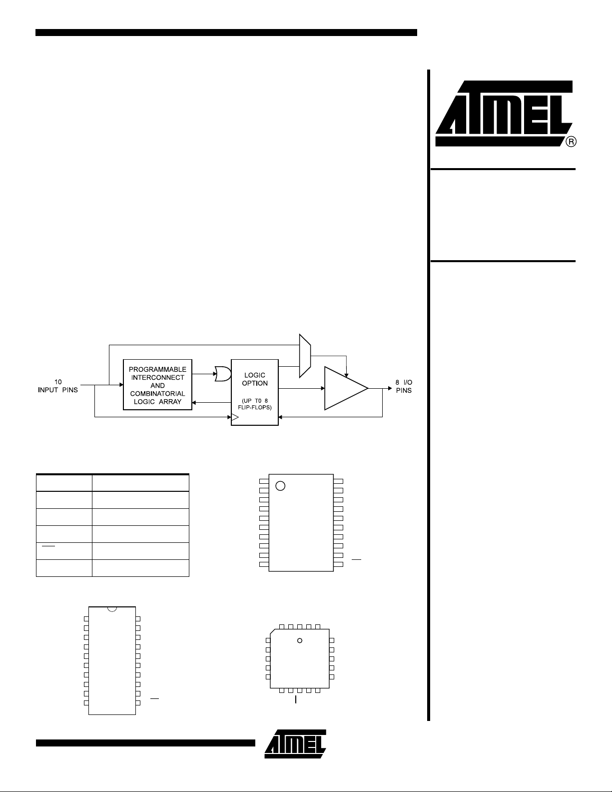
Block Diagram
Highperformance
EE PLD
ATF16V8CZ
Pin Configurations
All Pinouts Top View
Pin Name Function
CLK Clock
I Logic Inputs
I/O Bidirectional Buffers
OE
VCC +5V Supply
Output Enable
DIP/SOIC
I/CLK
GND
TSSOP
1
2
I1
3
I2
4
I3
5
I4
6
I5
7
I6
8
I7
9
I8
10
VCC
20
I/O
19
I/O
18
I/O
17
I/O
16
I/O
15
I/O
14
I/O
13
I/O
12
I9/OE
11
PLCC
I2I1I/CLK
VCC
I/O
321
20
19
18
I/O
17
16
15
14
I/O
I/O
I/O
I/O
I/O
I/O
Rev. 0453F–08/99
I3
I4
I5
I6
I7
4
5
6
7
8
910111213
I8
GND
I9/OE
1
Page 2
Description
The ATF16V8CZ is a high-perform ance EECMOS
Programmable Logic Device which utilizes Atmel’s proven
electrically-erasable Flash memory technology. Speeds
down to 12 ns and a 25 µA edge-sensing power-down
mode are offered. All speed ranges are specified over the
full 5V ± 10% range for industrial temperature ranges; 5V ±
5% for commercial range 5-volt devices.
The ATF16V8CZ incorporates a superset of the generic
architectures, wh ich allows di rect replac ement of th e 16R8
family and most 20-pin combinatorial PLDs. Ei ght outputs
are each allocated eight produc t terms. Three different
Absolute Maximum Ratings*
Temperature Under Bias.................................. -40°C to +85°C
Storage Temperature..................................... -65°C to +150°C
Voltage on Any Pin with
Respect to Ground .........................................-2.0V to +7.0V
Voltage on Input Pins
with Respect to Ground
During Programming.....................................-2.0V to +14.0V
Programming Voltage with
Respect to Ground .......................................-2.0V to +14.0V
(1)
(1)
(1)
modes of operation, configured automatically with software, allow highly complex logic functions to be realized.
The ATF16V8CZ can significantly reduce total system
power, thereby enhancing system reliability and reducing
power supply costs. Wh en al l the inpu ts an d inte rn al nodes
are not switchi ng, su pply cur rent dr ops to les s than 25 µA.
This automatic power-down feature allows for power
savings in slow clock systems and asynchronous applications. Also, the pin keeper circuits eliminate the need for
internal pull-up resistors along with their attendant power
consumption.
*NOTICE: Stresses beyond those listed under “Absolute
Maximum Ratings” may cause permanent damage to the device . This is a s tress rating only and
functional operatio n of the dev ice at th ese or an y
other conditions beyond those indicated in the
operational sections of this specification is not
implied. Exposure to absolute maximum rating
conditions for exten ded periods may af fect device
reliability.
Note: 1. Minimum voltage is -0.6V DC, which may under-
shoot to -2.0V for pulses of less than 20 ns.
Maximum output pin voltage is V
which may overshoot to 7.0V for pulses of less
than 20 ns.
+ 0.75V DC,
CC
DC and AC Operating Conditions
Commercial Industrial
Operating Temperature (Ambient) 0°C - 70°C-40°C - 85°C
V
Power Supply 5V ± 5% 5V ± 10%
CC
2
ATF16V8CZ
Page 3
ATF16V8CZ
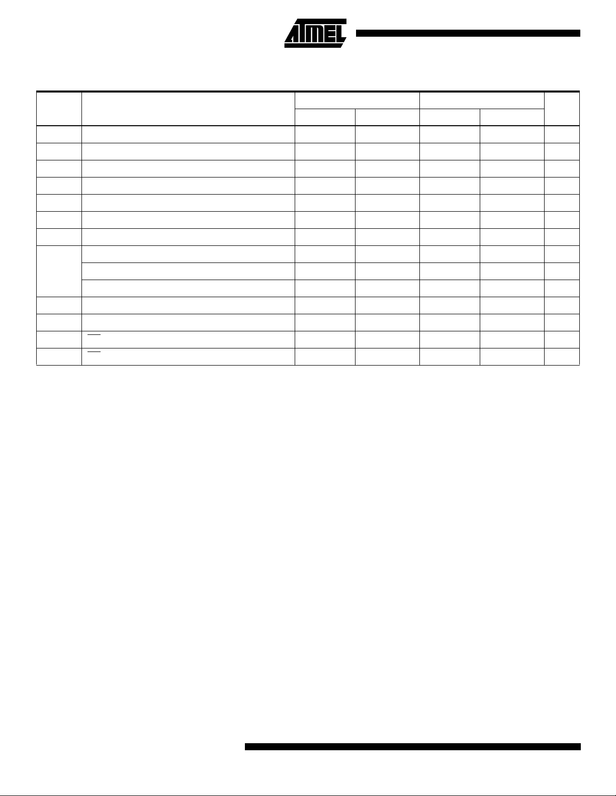
DC Characteristics
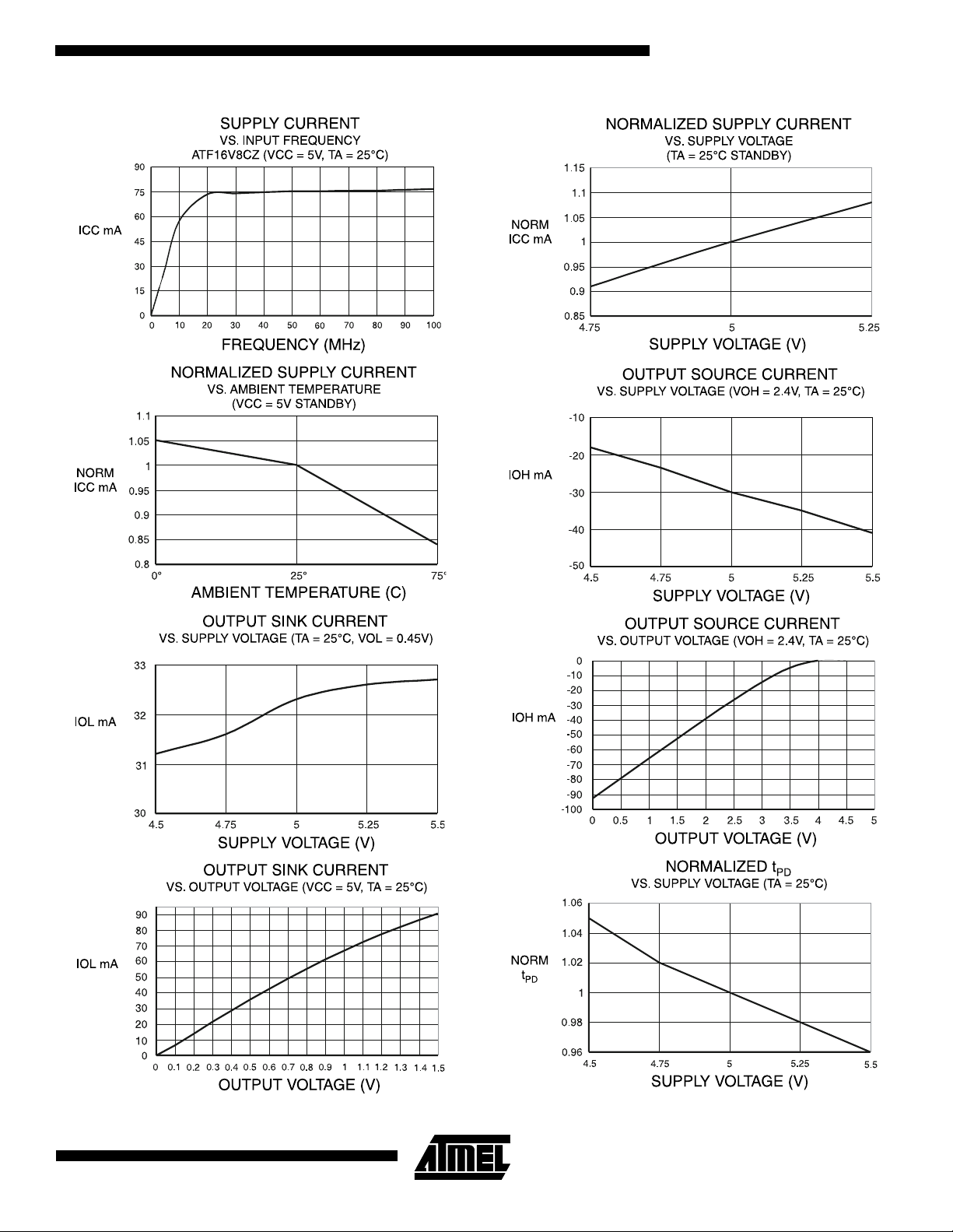
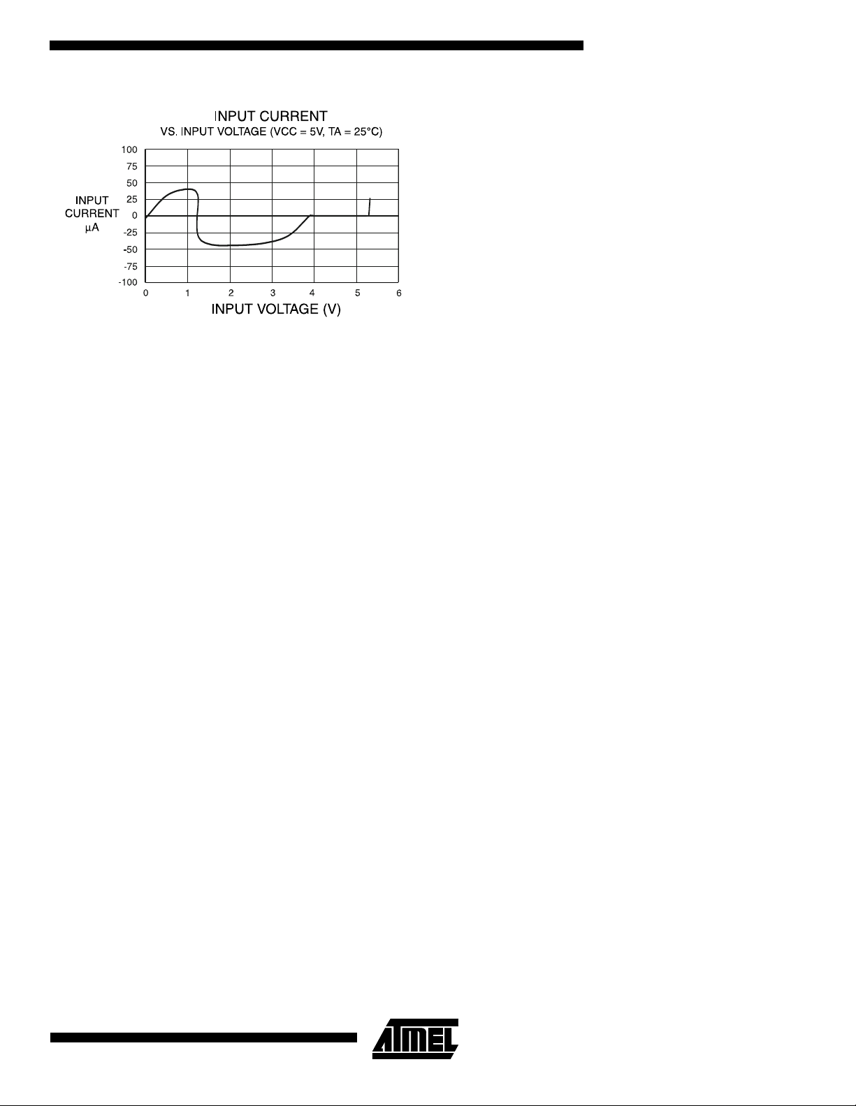
Symbol Parameter Condition Min Typ Max Units
I
IL
I
IH
I
CC1
Input or I/O Low Leakage Current 0 ≤ VIN ≤ VIL(Max) -10 µA
Input or I/O High Leakage Current 3.5 ≤ VIN ≤ V
Power Supply Current
15 MHz, V
V
IN
CC
= 0, VCC, Outputs Open
CC
= Max,
Com 95 mA
Ind. 105 mA
10 µA
(1)
I
CC
I
OS
V
IL
V
IH
V
OL
V
OH
I
OL
I
OH
Power Supply Current,
Standby Mode
Output Short Circuit Current
Input Low Voltage Min < VCC < Max -0.5 0.8 V
Input High Voltage 2.0 VCC+1 V
Output Low Current
Output Hi gh Current
Output Low Current VCC = Min
Output Hi gh Current VCC = Min Com., Ind. 4 mA
MHz, V
= 0, VCC, Outputs Open
V
IN
V
OUT
= 5V; TA = 25°C
V
CC
= Min, All Outputs
V
CC
= -16 mA
I
OL
= Min
V
CC
= -3.2 mA
I
OL
Note: 1. All ICC parameters measured with outputs open.
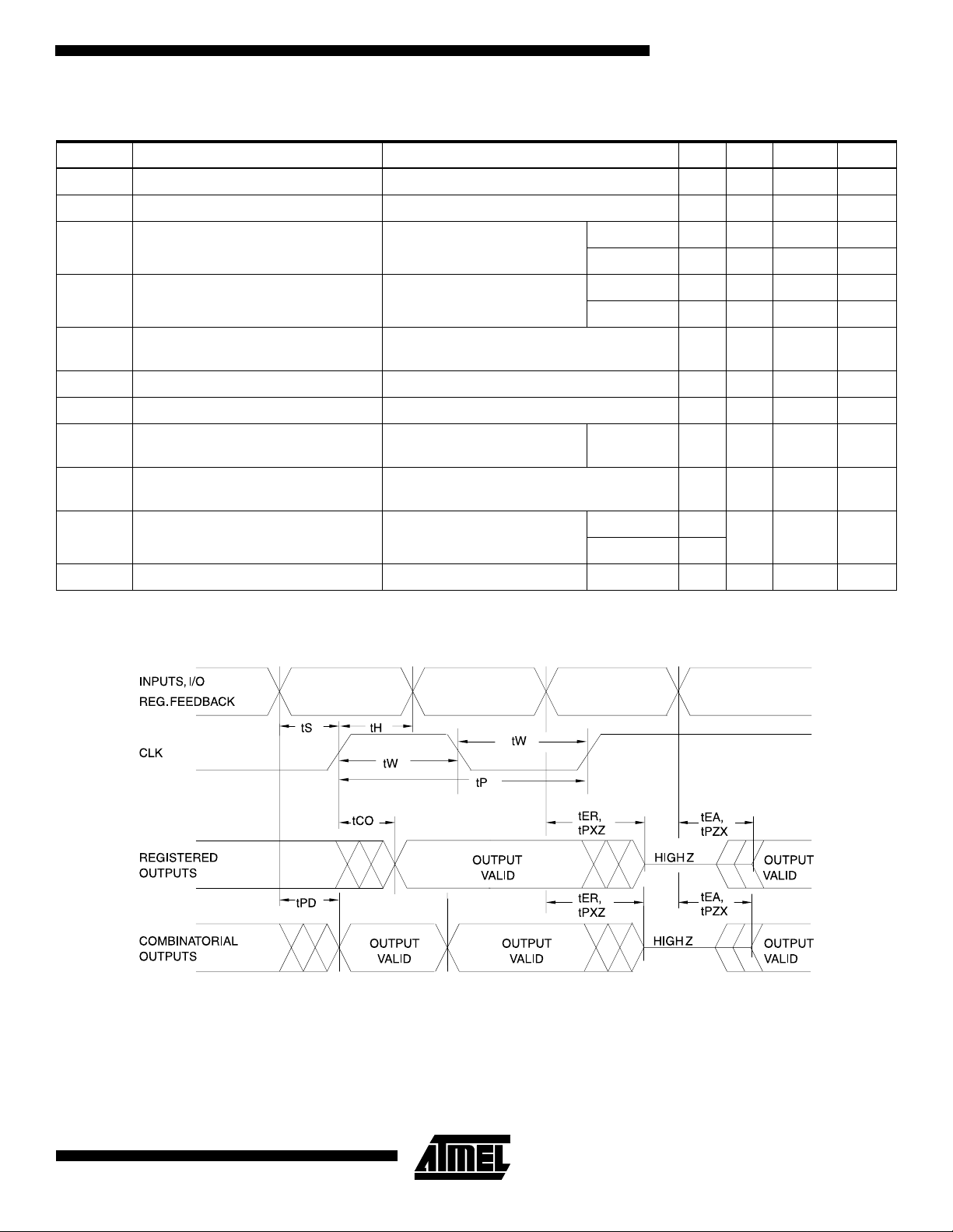
AC Waveforms
(1)
= Max,
CC
= 0.5V;
Com. 5 25
Ind 5 50
µA
µA
-150 mA
Com, Ind. 0.5 V
2.4 V
Com. 24 mA
Ind. 12
Note: 1. Timing measurement reference is 1.5V. Input AC driving levels are 0.0V and 3.0V, unless otherwise specified.
3
Page 4
AC Characteristics
Symbol Parameter
-12 -15
UnitsMin Max Min Max
t
t
t
t
t
t
t
F
t
t
t
t
PD
CF
CO
S
H
P
W
MAX
EA
ER
PZX
PXZ
Input or Feedback to Non-registered Output 3 12 3 15 ns
Clock to Feedback 6 8 ns
Clock to Output 2 8 2 10 ns
Input or Feedback Setup Time 10 12 ns
Input Hold Time 0 0 ns
Clock Period 12 16 ns
Clock Width 6 8 ns
External Feedback 1/(tS + tCO)5545MHz
Internal Feedback 1/(tS + tCF)6250MHz
No Feedback 1/(t
)8362MHz
P
Input to Output Enable – Product Term 3 12 3 15 ns
Input to Output Disable – Product Term 2 15 2 15 ns
OE pin to Output Enable 2 12 2 15 ns
OE pin to Output Disable 1.5 12 1.5 15 ns
4
ATF16V8CZ
Page 5

ATF16V8CZ
Input Test Waveforms and
Output Test Loads
Measurement Levels
tR, tF < 1.5 ns (10% to 90%)
Note: Similar devices are tested with slightly different loads.
These load differences may affect output signals’ delay
and slew rate. Atmel devices are tested with sufficient
margins to mee t compatible devices.
Pin Capacitance
f = 1 MHz, T = 25°C
C
IN
C
OUT
Note: 1. Typical values for nominal supply voltage. This parameter is only sampled and is not 100% tested.
(1)
Typ Max Units Conditions
58 pFV
68 pFV
= 0V
IN
OUT
= 0V
Power-up Reset
The ATF16V8CZ’s registers are designed to reset during
power-up. At a point delayed slightly from V
, all registers will be reset to th e low s tate. As a resul t,
V
RST
the registered output state will always be high on power-up.
This feature is critical for state machine initialization.
However, due to the asynchronous nature of reset and the
uncertainty of how V
actually rises in the system, the
CC
following conditions are required:
1. The V
rise must be monotonic, from below 0.7V,
CC
2. After reset occurs, all input and feedback setup
times must be met before driving the clock term
high, and
3. The signals from which the clock is derived must
remain stable during t
PR
.
crossing
CC
Parameter Description Typ Max Units
t
PR
V
RST
Power-up Reset Time 600 1,000 ns
Power-up Reset Voltage 3.8 4.5 V
5
Page 6
Registered Output Preload
The ATF16V8CZ’s registers are provided with circuitry to
allow loading of each register with either a high or a low.
This feature will simplify testing since an y state can be
forced into the registers to control test sequenc ing. A
JEDEC file with preload is generated whe n a source file
with vectors is compiled. Once downloaded, the JEDEC file
preload sequence will be done automaticall y by approved
programmers.
Security Fuse Usage
A single fuse is provided to pre vent unauthorized copying
of the ATF16V8CZ fuse patterns. Once programmed, fuse
verify and preload are in hibited. Howev er, the 64-bit Us er
Signature remains accessible.
The security fuse should be programmed last, as its effect
is immediate.
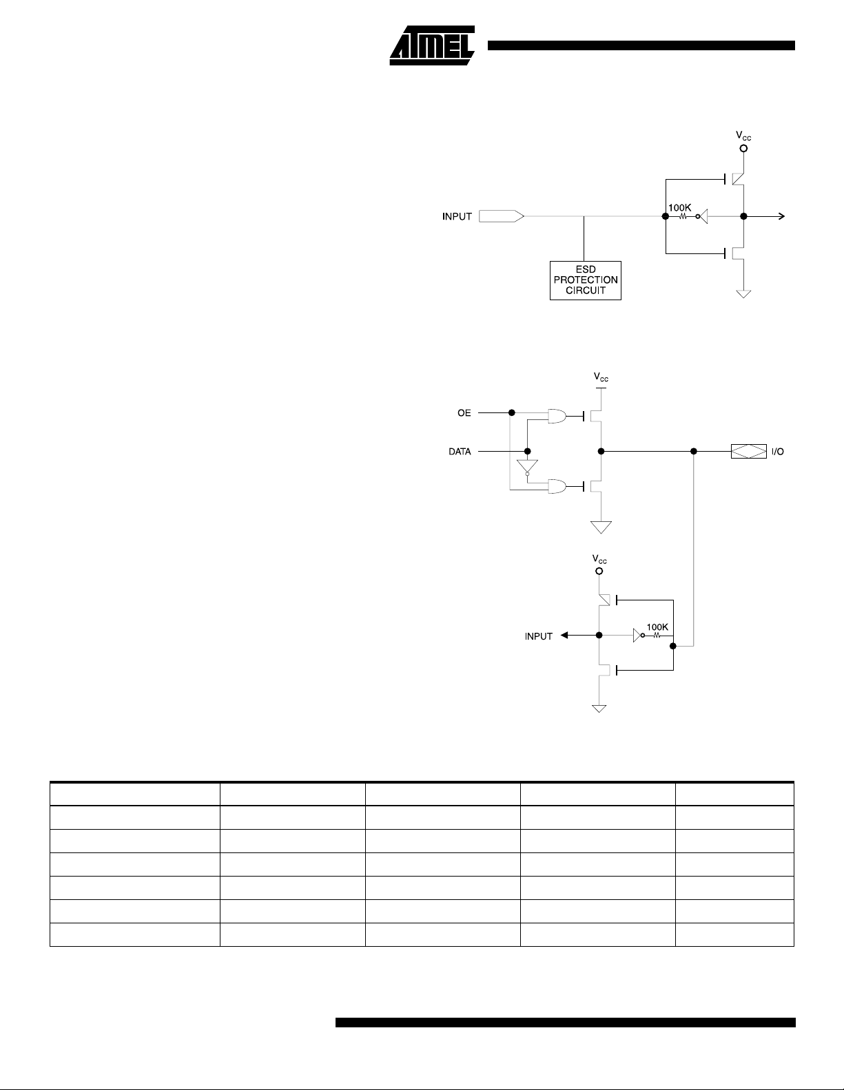
Input and I/O Pin Keeper Circuits
The ATF16V8CZ contains inte rnal i nput and I/O pin kee per
circuits. These circuits allow each ATF16V8CZ pin to hold
its previous value even when it is not being driven by an
external source or by the devi ce's output buffe r. This helps
insure that all logic array inputs are at known, valid logic
levels. This redu ces s ystem power b y preven ting pi ns fro m
floating to indeterminate levels. By using pin keeper circuits
rather than pull-up resistors, there is no DC current
required to hold the pins in either logic state (high or low).
These pin keeper circui ts are implemen ted as weak feedback inverters, as s hown in the Input Di agram below.
These keeper circuits c an ea si ly be over dr iven by standard
TTL- or CMOS-compatible driver s. The typical ove rdrive
current required is 40 µA.
Input Diagram
I/O Diagram
Compiler Mode Selection
Registered Complex Simple Auto Select
ABEL, Atmel-ABEL P16C8R P16V8C P16V8AS P16V8
CUPL G16V8MS G16V8MA G16V8AS G16V8A
LOG/iC GAL16V8_R
OrCAD-PLD “Registered”“Complex”“Simple” GAL16V8A
PLDesigner P16V8R P16V8C P16V8C P16V8A
Tango-PLD G16V8R G16V8C G16V8AS G16V8
Note: 1. Only applicable for version 3.4 or lower.
6
ATF16V8CZ
(1)
GAL16V8_C7
(1)
GAL16V8_C8
(1)
GAL16V8
Page 7
ATF16V8CZ
7
Page 8

8
ATF16V8CZ
Page 9
ATF16V8CZ
9
Page 10

Ordering Information
t
PD
(ns)
12 10 8 ATF16V8CZ-12JC
15 12 10 ATF16V8CZ-15JC
t
S
(ns)
12 10 ATF16V8CZ-15JI
t
CO
(ns) Ordering Code Package Operation Range
ATF16V8CZ-12PC
ATF16V8CZ-12SC
ATF16V8CZ-12XC
ATF16V8CZ-15PC
ATF16V8CZ-15SC
ATF16V8CZ-15XC
ATF16V8CZ-15PI
ATF16V8CZ-15SI
ATF16V8CZ-15XI
20J
20P3
20S
20X
20J
20P3
20S
20X
20J
20P3
20S
20X
Commercial
(0°C to 70°C)
Commercial
(0°C to 70°C)
Industrial
(-40°C to 85°C)
Using “C” Product for Industrial
To use commercial product for Industrial temperature ranges, down-grade one speed grade from the “I” to the “C” device
(7 ns “C” = 10 ns “I”) and de-rate power by 30%.
Package Type
20J 20-lead, Plastic J-leaded Chip Carrier (PLCC)
20P3 20-lead, 0.300" Wide, Plastic Dual Inline Package (PDIP)
20S 20-lead, 0.300" Wide, Plastic Gull-wing Small Outline (SOIC)
20X 20-lead, 4.4 mm Wide, Plastic Thin Shrink Small Outline (TSSOP)
10
ATF16V8CZ
Page 11
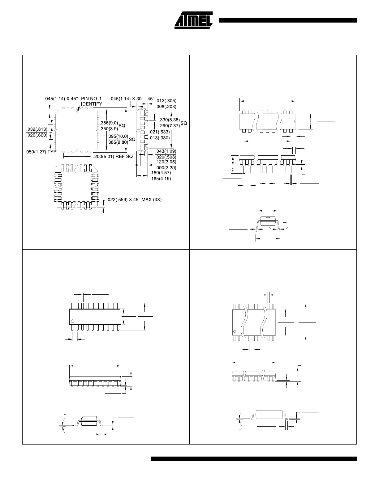
Packaging Information
PIN 1 ID
20J, 20-lead, Plastic J-leaded Chip Carrier (PLCC)
Dimensions in Inches and (Millimeters)
JEDEC STANDARD MS-018 AA
20P3, 20-lead, 0.300" Wide,
Plastic Dual Inline Package (PDIP)
Dimensions in Inches and (Millimeters)
JEDEC STANDARD MS-001 AD
1.060(26.9)
.210(5.33)
SEATING
PLANE
.980(24.9)
.900(22.86) REF
MAX
.150(3.81)
.115(2.92)
.110(2.79)
.090(2.29)
.014(.356)
.008(.203)
PIN
1
.070(1.78)
.045(1.13)
.325(8.26)
.300(7.62)
0
REF
15
.430(10.92) MAX
.022(.559)
.014(.356)
.280(7.11)
.240(6.10)
.090(2.29)
MAX
.005(.127)
MIN
.015(.381) MIN
20S, 20-lead, 0.300" Wide, Plastic Gull-wing Small
Outline (SOIC)
Dimensions in Inches and (Millimeters)
0.020 (0.508)
0.013 (0.330)
0.420 (10.7)
0.299 (7.60)
0.393 (9.98)
0.012 (0.305)
0.003 (0.076)
0.291 (7.39)
0.013 (0.330)
0.009 (0.229)
0.105 (2.67)
0.092 (2.34)
PIN 1
0
8
REF
.050 (1.27) BSC
0.035 (0.889)
0.015 (0.381)
0.513 (13.0)
0.497 (12.6)
20X, 20-lead, 4.4 mm Wide, Plastic Thin Shrink
Small Outline (TSSOP)
Dimensions in Millimeters and (Inches)*
0.30(0.012)
0.18(0.007)
PIN 1 ID
0
REF
8
6.60(.260)
6.40(.252)
0.70(.028)
0.50(.020)
4.48(.176)
4.30(.169)
0.65(.0256) BSC
0.15(.006)
0.05(.002)
6.50(.256)
6.25(.246)
1.10(0.043) MAX
0.18(.007)
0.09(.003)
*Controlling dimension: millimeters
11
ATF16V8CZ
Page 12

Atmel Headquarters Atmel Operations
Corporate Headquarters
2325 Orchard Parkway
San Jose, CA 95131
TEL (408) 441- 0311
FAX (408) 487-2600
Europe
Atmel U.K., Ltd.
Coliseum Business Centre
Riverside Way
Camberley, Surrey GU15 3YL
England
TEL (44) 1276-686-677
FAX (44) 1276-686-697
Asia
Atmel Asia, Ltd.
Room 1219
Chinachem Golden Plaza
77 Mody Road Tsimhatsui
East Kowloon
Hong Kong
TEL (852) 2721- 9778
FAX (852) 2722-1369
Japan
Atmel Japan K.K.
9F, Tonetsu Shinkawa Bldg.
1-24-8 Shinka wa
Chuo-ku, Tokyo 104-0033
Japan
TEL (81) 3-3523-3551
FAX (81) 3-3523-7581
Atmel Colorado Springs
1150 E. Cheyenne Mtn. Blvd.
Colorado Springs, CO 80906
TEL (719) 576-3300
FAX (719) 540-1759
Atmel Rousset
Zone Indus triel le
13106 Rousset Cedex
France
TEL (33) 4-4253-6000
FAX (33) 4-4253-6001
Fax-on-Demand
North America:
1-(800) 292-8635
International:
1-(408) 441-0732
e-mail
literature@atmel.com
Web Site
http://www.atmel.com
BBS
1-(408) 436-4309
© Atmel Corporation 1999.
Atmel Corporation makes no warranty for the use of its products, other than those expressly contained in the Company’s standard warranty which is detailed in Atmel’s Terms and Conditions located on the Company’s web site. The Company assumes no responsibility for
any errors which may appear in this document, reserves the right to change devices or specifications detailed herein at any time without
notice, and does not make any commitment to update the information contained herein. No licenses to patents or other intellectual property of Atmel are granted by the Company in connection with the sale of Atmel products, expressly or by implication. Atmel’s products are
not authorized for use as critical components in life support devices or systems.
Marks bearing ® and/or ™ are regi stered trad emar ks and trad emark s of A tmel C orp oratio n.
Terms and product names in this document may be trademarks of others.
Printed on recycled paper.
0453F–08/99/xM
 Loading...