

Page 1
Features
• Industry-standard Architecture
– Emulates Many 20-pin PALs
– Low-cost Easy-to-use Software Tools
• High-speed Electrically-erasable Programmable Logic Devices
– 5 ns Maximum Pin-to-pin Delay
• Low-power - 100 µA Pin-controlled Power-down Mode Option
• CMOS and TTL Compatible Inputs and Outputs
– I/O Pin Keeper Circuits
• Advanced Flash Technology
– Reprogrammable
– 100% Tested
• High-reliability CMOS Process
– 20 Year Data Retention
– 100 Erase/Write Cycles
– 2,000V ESD Protection
– 200 mA Latchup Immunity
• Commercial and Industrial Temperature Ranges
• Dual-in-line and Surface Mount Packages in Standard Pinouts
• PCI Compliant
®
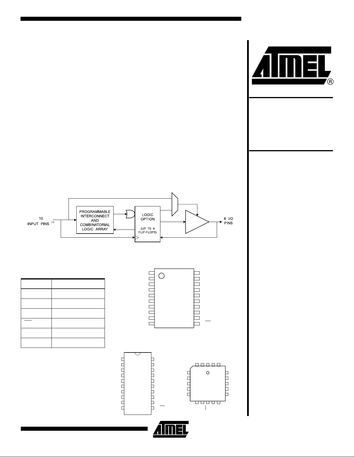
Block Diagram
Highperformance
EE PLD
ATF16V8C
Note: 1. Includes optional PD control pin.
Pin Configurations
All Pinouts Top View
Pin Name Function
CLK Clock
I Logic Inputs
I/O Bidirectional Buffers
OE
VCC +5V Supply
PD Power-down
Output Enable
I/CLK
I1
I2
PD/I3
I4
I5
I6
I7
I8
GND
I/CLK
PD/I3
GND
DIP/SOIC
1
2
3
4
5
6
7
8
9
10
TSSOP
1
2
I1
3
I2
4
5
I4
6
I5
7
I6
8
I7
9
I8
10
VCC
20
I/O
19
I/O
18
I/O
17
I/O
16
I/O
15
I/O
14
I/O
13
I/O
12
I9/OE
11
PLCC
20
VCC
19
I/O
18
I/O
17
I/O
16
I/O
15
I/O
14
I/O
13
I/O
12
I/O
11
I9/OE
PD/I3
I4
I5
I6
I7
I2I1I/CLK
321
4
5
6
7
8
910111213
I8
GND
I9/OE
VCC
20
I/O
I/O
19
18
17
16
15
14
I/O
I/O
I/O
I/O
I/O
I/O
Rev. 0425G–08/99
1
Page 2
Description
The ATF16V8C is a high -perfor manc e EEC MOS Pr ogra mmable Logic Device that utilizes Atmel’s proven electricallyerasable Flash memory technology. Speeds down to 5 ns
and a 100 µA pin-controlled power-down mode option are
offered. All speed ranges are specified over the full 5V ±
10% range for industrial temperature ranges; 5V ± 5% for
commercial range 5-volt devices.
The ATF16V8C incorporates a s uperset of the ge neric
architectures, wh ich allows di rect replac ement of th e 16R8
family and most 20-pin combinatorial PLDs. Ei ght outputs
are each allocated eight produc t terms. Three different
Absolute Maximum Ratings*
Temperature Under Bias.................................. -40°C to +85°C
Storage Temperature..................................... -65°C to +150°C
Voltage on Any Pin with Respect to Ground...-2.0V to +7.0V
Voltage on Input Pins
with Respect to Ground
During Programming.....................................-2.0V to +14.0V
Programming Voltage with
Respect to Ground .......................................-2.0V to +14.0V
(1)
(1)
(1)
modes of operation, configured automatically with software, allow highly complex logic functions to be realized.
The ATF16V8C can significantly reduce total system
power, thereby enhancing system reliability and reducing
power supply costs. When pin 4 is configured as the
power-down control pin, supply current drops to less than
100 µA whenever the pin is high. If the power-down feature
isn't required for a particular application, pin 4 may be used
as a logic input. Also, the pin keeper circuits eliminate the
need for internal pu ll -up r es isto rs a lon g wi th t hei r atte nda nt
power consumption.
*NOTICE: Stresses beyond those listed under “Absolute
Maximum Ratings” may cause permanent damage to the device . This is a s tress rating only and
functional operatio n of the dev ice at th ese or an y
other conditions beyond those indicated in the
operational sections of this specification is not
implied. Exposure to absolute maximum rating
conditions for exten ded periods may af fect device
reliability.
Note: 1. Minimum voltage is -0.6V DC, which may under-
shoot to -2.0V for pulses of less than 20 ns.
Maximum output pin voltage is V
which may overshoot to 7.0V for pulses of less
than 20 ns.
+ 0.75V DC,
CC
DC and AC Operating Conditions
Commercial Industrial
Operating Temperature (Ambient) 0°C - 70°C-40°C - 85°C
V
Power Supply 5V ± 5% 5V ± 10%
CC
2
ATF16V8C
Page 3
ATF16V8C
DC Characteristics
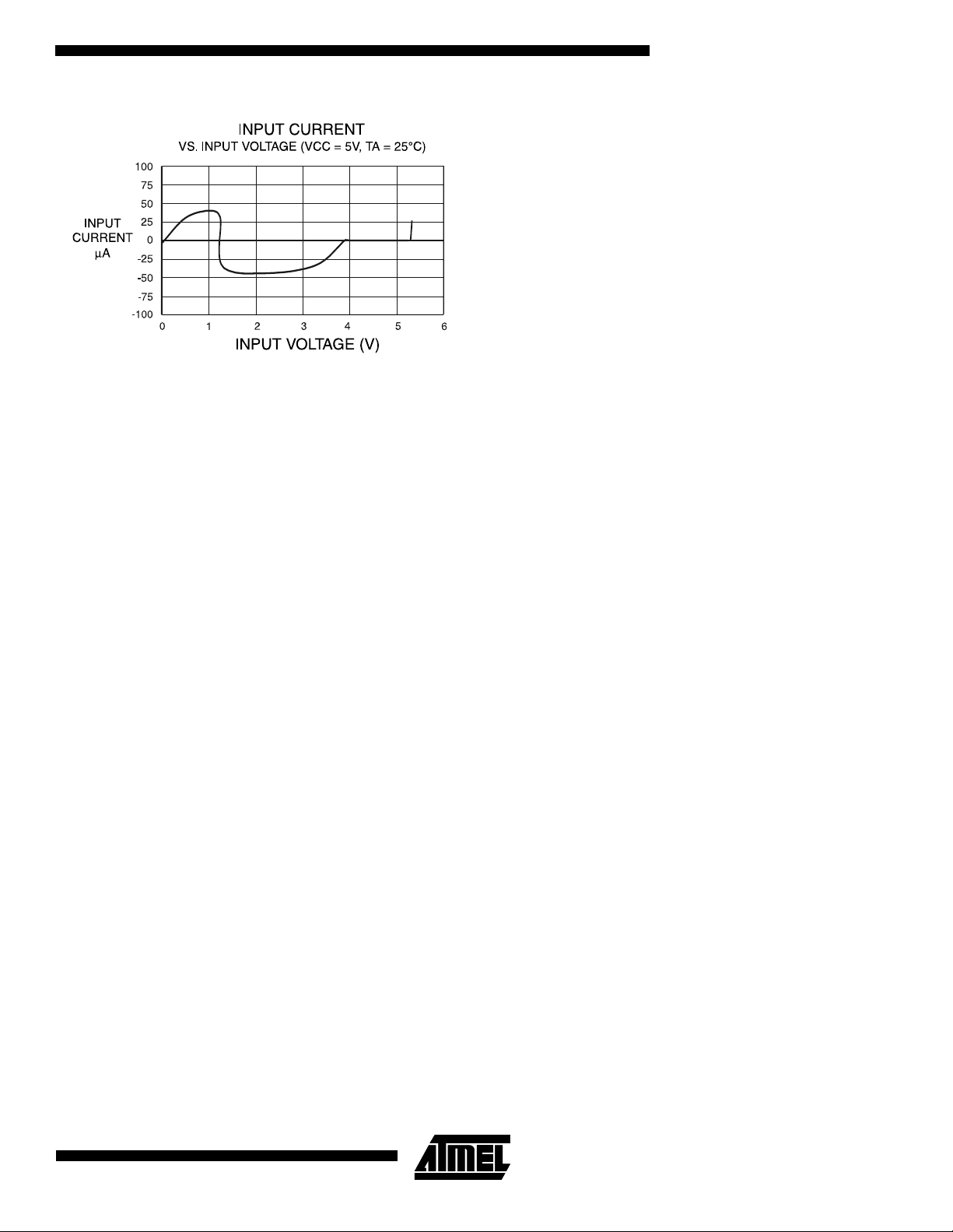
Symbol Parameter Condition Min Typ Max Units
I
I
I
IL
IH
CC1
Input or I/O Low Leakage Current 0 ≤ VIN ≤ VIL (Max) -10.0 µA
Input or I/O High Leakage Current 3.5 ≤ VIN ≤ V
(1)
Power Supply Current, Standby
15 MHz, V
V
= 0, VCC, Outputs Open
IN
CC
= Max,
CC
Com. 115 mA
Ind. 130 mA
10.0 µA
I
PD
I
OS
V
IL
V
IH
V
OL
V
OH
I
OL
I
OH
Power Supply Current,
Power-down Mode
Output Short Circuit Current V
= Max, VIN = 0, V
V
CC
= 0.5V;
OUT
= 5V; TA = 25°C
V
CC
Input Low Voltage Min < VCC < Max -0.5 0.8 V
Input High Voltage 2.0 VCC + 1 V
= Min; All Outputs
V
Output Low Voltage
Output High Voltage
CC
= 24 mA
I
OL
= Min
V
CC
= -4.0 mA
I
OL
Output Low Current VCC = Min
Output High Current VCC = Min Com., Ind. -4.0 mA
Note: 1. All ICC parameters measured with outputs open.
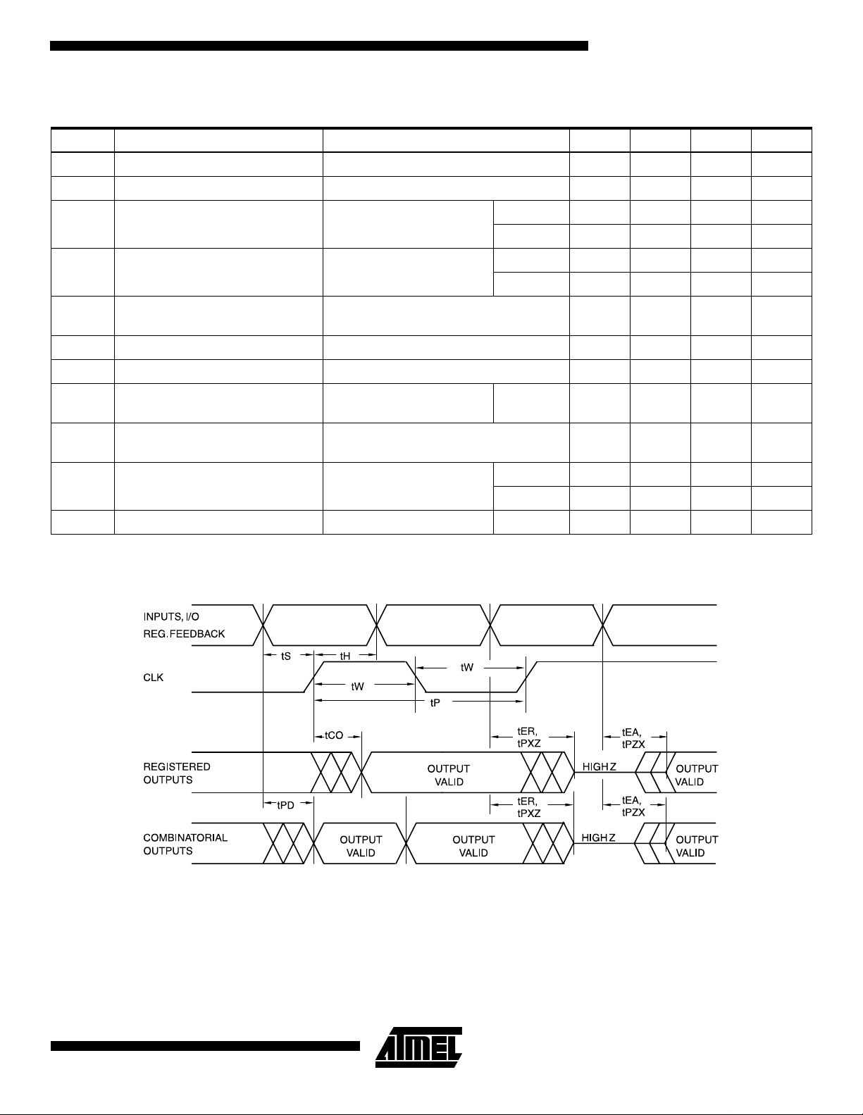
AC Waveforms
CC
Com. 10 100 µA
Ind. 10 105
µA
-150 mA
Com., Ind. 0.5 V
2.4 V
Com. 24.0 mA
Ind. 12.0 mA
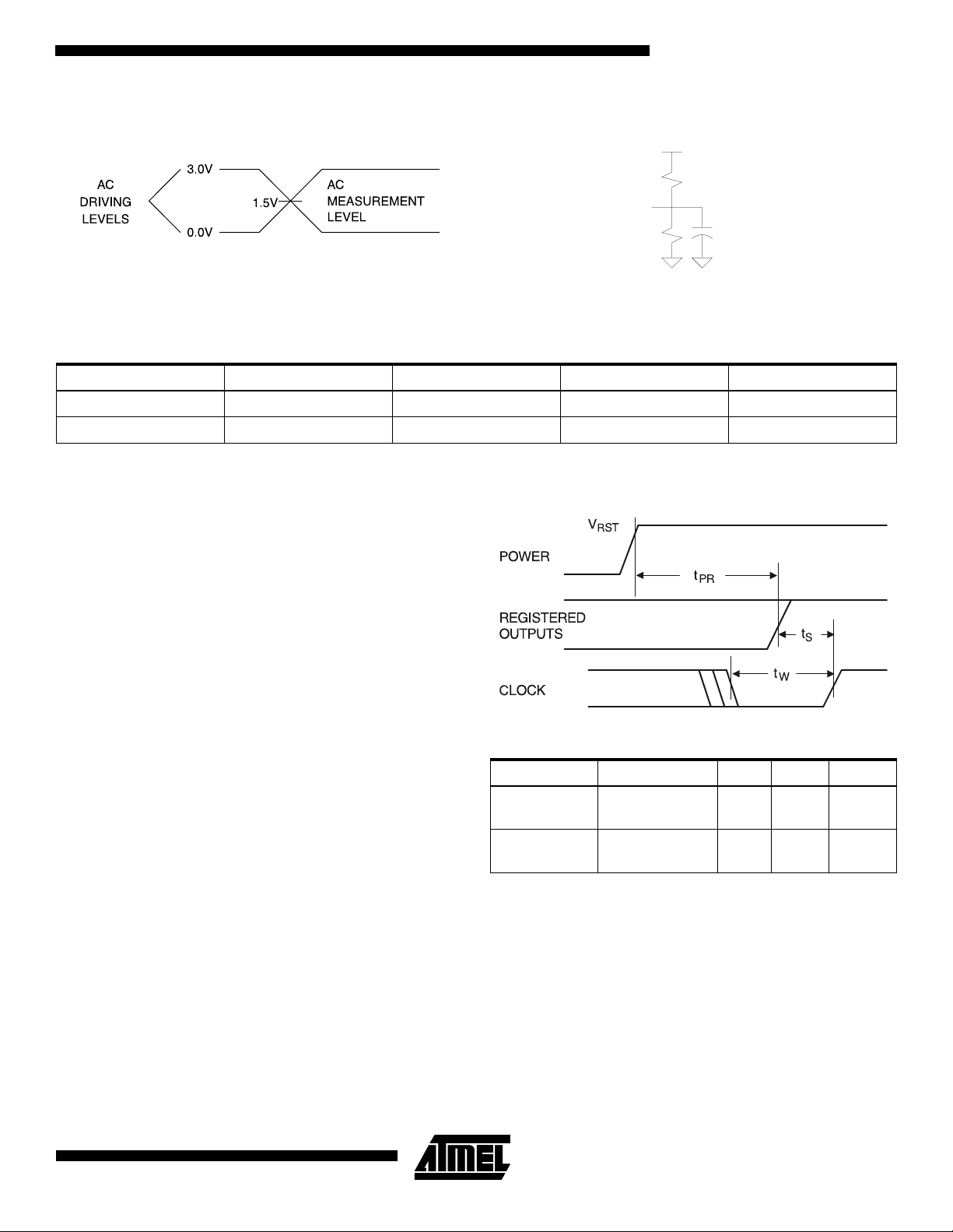
Note: 1. Timing measurement reference is 1.5V. Input AC driving levels are 0.0V and 3.0V, unless otherwise specified.
3
Page 4
AC Characteristics
Symbol Parameter
-5 -7
UnitsMin Max Min Max
t
PD
t
CF
t
CO
t
S
t
H
t
P
t
W
Input or Feedback to Non-Registered Output 1 5 3 7.5 ns
Clock to Feedback 3 3 ns
Clock to Output 1425ns
Input or Feedback Setup Time 3 5 ns
Input Hold Time 0 0 ns
Clock Period 6 8 ns
Clock Width 3 4 ns
External Feedback 1/(tS + tCO) 142 100 MHz
F
t
t
t
t
MAX
EA
ER
PZX
PXZ
Internal Feedback 1/(tS + tCF) 166 125 MHz
No Feedback 1/(t
) 166 125 MHz
P
Input to Output Enable – Product Term2639ns
Input to Output Disable – Product Term2529ns
OE pin to Output Enable 2526ns
OE pin to Output Disable 1.5 5 1.5 6 ns
Power-down AC Characteristics
(1)(2)(3)
-5 -7
Symbol Parameter
t
IVDH
t
GVDH
t
CVDH
t
DHIX
t
DHGX
t
DHCX
t
DLIV
t
DLGV
t
DLCV
t
DLOV
Valid Input Before PD High 5.0 7.5 ns
Valid OE Before PD High 0 0 ns
Valid Clock Before PD High 0 0 ns
Input Don’t Care After PD High 5.0 7.5 ns
OE Don’t Care After PD High 5.0 7.5 ns
Clock Don’t Care After PD High 5.0 7.5 ns
PD Low to Valid Input 5.0 7.5 ns
PD Low to Valid OE 15.0 20.0 ns
PD Low to Valid Clock 15.0 20.0 ns
PD Low to Valid Output 20.0 25.0 ns
Notes: 1. Output data is latched and held.
2. HI-Z outputs remain HI-Z.
3. Clock and input transitions are ignored.
UnitsMin Max Min Max
4
ATF16V8C
Page 5
ATF16V8C
Input Test Waveforms and Measurement Levels:
Output Test Loads:
5.0V
R1 = 200
R2 = 200
OUTPUT
PIN
CL = 50 pF
tR, tF < 1.5 ns (10% to 90%)
Pin Capacitance
(1)
f = 1 MHz, T = 25°C
Typ Max Units Conditions
C
IN
C
OUT
Note: 1. Typical values for nominal supply voltage. This parameter is only sampled and is not 100% tested.
58pFV
68pFV
Power-up Reset
The ATF16V8C ’s registers are designed to reset during
power-up. At a point delayed slightly from V
, all registers will be reset to th e low s tate. As a resul t,
V
RST
the registered output state will always be high on power-up.
This feature is critical for state machine initialization.
However, due to the asynchronous nature of reset and the
uncertainty of how V
actually rises in the system, the
CC
following conditions are required:
1. The V
rise must be monotonic, from below 0.7V,
CC
2. After reset occurs, all input and feedback setup
times must be met before driving the clock term
high, and
3. The signals from which the clock is derived must
remain stable during t
PR
.
crossing
CC
Parameter Description Typ Max Units
t
PR
V
RST
Power-up
Reset Time
Power-up
Reset Voltage
600 1,000 ns
3.8 4.5 V
= 0V
IN
OUT
= 0V
5
Page 6
Power-down Mode
The ATF16V8C includes an optional pin controlled powerdown feature. Dev ice pin 4 may be configur ed as the
power-down pin. When this feature is enabled and the
power-down pin is high, total curren t consumption dr ops to
less than 100 µ A. I n the p ower-do wn mode , all output data
and internal logic states are latched and held. All registered
and combinator ial output da ta remains v alid. Any ou tputs
which were in a HI-Z state at the onset of power-down will
remain at HI-Z. During power-down, all input signals except
the power-down pin are blocked. T he input and I/O pin
keeper circuits remain ac tiv e to in su re that pin s do not floa t
to indeterminate levels. This helps to further reduce system
power.
Selection of the power-down option is specified in the
ATF16V8C logi c de sign f ile. The log ic com pile r wi ll in clud e
this option selection in the otherwise standard 16V8
JEDEC fuse file. When the power-down feature is not specified in the design file, pin 4 is available as a logic input, and
there is no power-down pin. This allows the ATF16V8C to
be programmed using any existing standard 16V8 fuse file.
Note: Some programmers list the JEDEC-compatible 16V8C
(No PD used) separately from the non-JEDEC compatible 16V8CEXT. (EXT for extended features.)
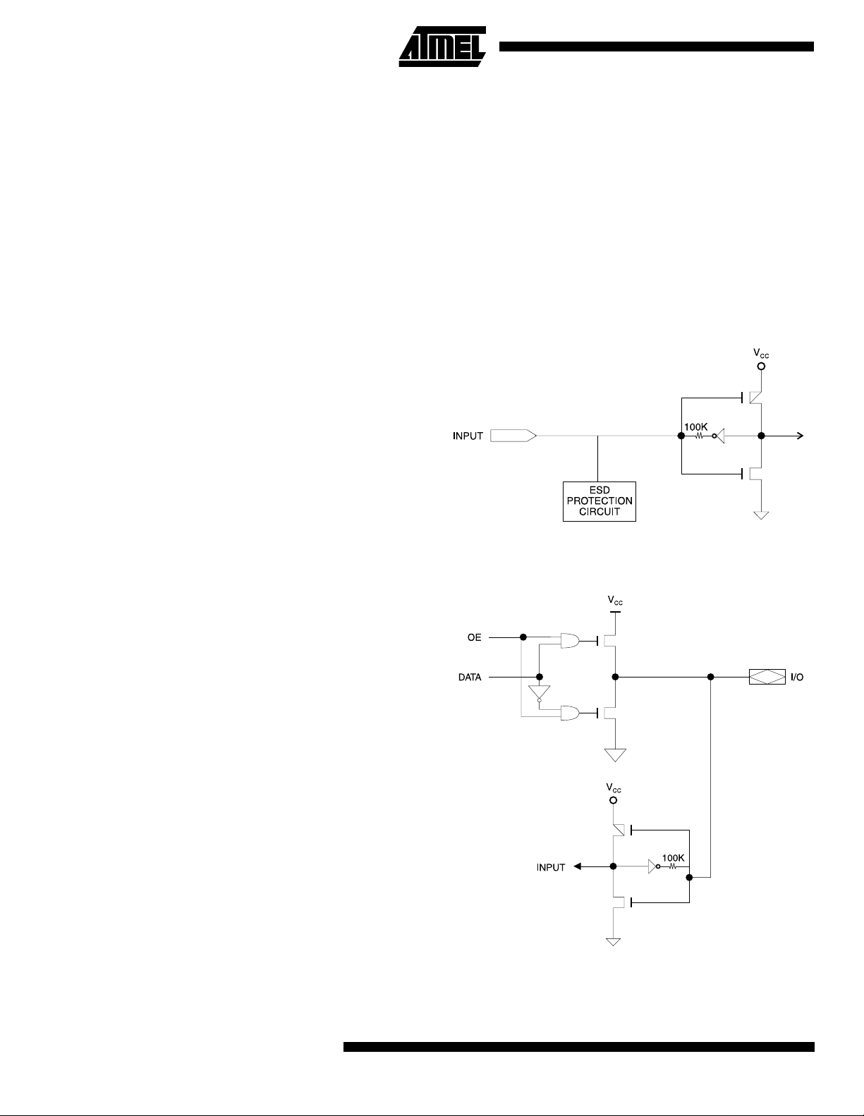
external source or by the device’s output buffer. This helps
insure that all logic array inputs are at known, valid logic
levels. This redu ces s ystem power b y preven ting pi ns fro m
floating to indeterminate levels. By using pin keeper circuits
rather than pull-up resistors, there is no DC current
required to hold the pins in either logic state (high or low).
These pin keeper circuits are implemented a s weak feedback inverters, as shown in the Inp ut Diagram below.
These keeper circuits c an ea si ly be ov er driv en by s tand ard
TTL- or CMOS-compatible driver s. The typical ove rdrive
current required is 40 µA.
Input Diagram
Registered Output Preload
The ATF16V8C’s registers are provided with circuitry to
allow loading of each register with either a high or a low.
This feature will simplify testing since an y state can be
forced into the registers to control test sequenc ing. A
JEDEC file with preload is generated whe n a source file
with vectors is compiled. Once downloaded, the JEDEC file
preload sequence will be done automaticall y by approved
programmers.
Security Fuse Usage
A single fuse is provided to pre vent unauthorized copying
of the ATF16V8C fuse patterns. Once programmed, fuse
verify and preload are in hibited. Howev er, the 64-bit Us er
Signature remains accessible.
The security fuse will be programmed last, as its effect is
immediate.
Input and I/O Pin Keeper Circuits
The ATF16V8C contains internal input and I/O pin keeper
circuits. These circuits allow each ATF16V8C pin to hold its
previous value even when it is not being driven by an
I/O Diagram
6
ATF16V8C
Page 7

Functional Logic Diagram Description
ATF16V8C
The Logic Option and Fu nctional Diagrams des cribe the
ATF16V8C archite cture. Eigh t config urable macr ocells ca n
be configured as a registered output, combinatorial I/O,
combinatorial output, or dedicated input.
The ATF16V8C can be configured in one of three different
modes. Each mode makes the ATF16V8C look like a different device. Most PLD compilers can choose the right mode
automatically. The user can also force the selection by supplying the compile r with a m ode selection. The det er min in g
factors would be the usage of register versus combinatorial
outputs and dedicated o utputs versus ou tputs with outp ut
enable control.
The ATF16V8C univers al archite cture can be progra mmed
subsets can be found in ea ch of the con figurat ion modes
described in the foll owing pages . The user can do wnload
the listed sub set device JEDEC progr amming fil e to the
PLD programmer, and the ATF16V8C can be configured to
act like the chosen device. Check with your programmer
manufacturer for this capability.
Unused product terms are automat ically disab led by the
compiler to decrease power consumption. A Security Fuse,
when programmed, protec ts the con tent of the ATF 16V8 C.
Eight bytes (64 fuses) of User Signature are accessible to
the user for purposes such as storing project name, part
number, revision, or date. The User Signature is accessible
regardless of the state of the Security Fuse.
to emulate many 20-pin PAL devi ces. The se architectu ral
Compiler Mode Selection
Registered Complex Simple Auto Select
ABEL, Atmel-ABEL P16V8R P16V8C P16V8AS P16V8
With PD ENABLE P16V8PDR
CUPL, Atmel-CUPL G16V8MS G16V8MA G16V8AS G16V8A
With PD ENABLE G16V8CPMS G16V8CPMA G16V8CP AS G16V8CP
LOG/iC GAL16V8_R
OrCAD-PLD “Registered”“Complex”“Simple” GAL16V8A
(1)
(2)
P16V8PDC
GAL16V8_C7
(1)
(2)
P16V8PD
GAL16V8_C8
(1)
(2)
P16V8PDS
GAL16V8
(1)
PLDesigner P16V8R P16V8C P16V8C P16V8A
Synario/Atmel-Synario NA NA NA ATF16V8C ALL
With PD ENABLE NA NA NA ATF16V8C (PD) ALL
Tango-PLD G16V8R G16V8C G16V8AS G16V8
Notes: 1. Please call Atmel PLD Hotline at (408) 436-4333 for more informati on.
2. Only applicable for version 3.4 or lower.
(1)
7
Page 8

Macrocell Configuration
Software compilers support the three different OMC modes
as different device types. These device types are l isted in
the table below. Most compilers have the ability to automatically select the device type, gener ally based on the
register usage and output enable (OE
usage on the device for c es the s oft war e to cho os e th e r egistered mode. All combinatorial outputs with OE
by the product term will force the software to choose the
complex mode. The software will choose the simple mode
only when all outputs are ded icated combi natorial witho ut
control. The di fferent devi ce types listed in the tabl e
OE
can be used to override the automatic device selection by
the software. For further details, re fer to the compiler s oftware manuals.
When using compiler software to configure the device, the
user must pay special attentio n to the follow ing rest rictions
in each mode.
In registered mode pin 1 and pin 11 are permanen tly c onfigured as clock and output enable, respectively. These
pins cannot be c onfigu red as de dica ted i nputs in th e re gistered mode.
In compl ex mode pin 1 and pin 11 becom e dedicated
inputs and use the feedback paths of pin 19 and pin 12
respectively. Because of this feedback path usage, pin 19
and pin 12 do not have the feedback option in this mode.
In simple mode all feedback paths of the output pins are
routed via the adjacent pins. In doing so, the two inner most
pins (pins 15 and 16) will not have the feedback option as
these pins are always configured as dedicated combinatorial output.
) usage. Register
controlled
Registered Configuration for
Registered Mode
Notes: 1. Pin 1 controls common CLK for the registered
outputs.
Pin 11 controls common OE for the registered
outputs.
Pin 1 and Pin 11 are permanently configured as
CLK and OE
2. The development software configures all the architecture control bits and checks for proper pin usage
automatically.
(1)(2)
.
Combinatorial Configuration for
Registered Mode
(1)(2)
ATF16V8C Registered Mode
PAL Device Emulation/PAL Replacement
The registered mode is used if one or more registers are
required. Each macrocell can be configured as either a registered or combinat orial output or I/O, or as an input. F or a
registered output or I/O, the output is enabled by the OE
pin, and the regist er is clocked by the CLK pi n. Eight
product terms are allocated to the sum term. For a combinatorial output or I/O, the output enable is controlled by a
product term, and s ev en prod uc t te r ms are al lo ca ted to the
sum term. When the macrocell is configured as an input,
the output enable is permanently disabled.
Any register usage will make the compiler select this mode.
The following r egistered de vices can be emulate d using
this mode:
16R8 16RP8
16R6 16RP6
16R4 16RP4
8
ATF16V8C
Notes: 1. Pin 1 and Pin 11 are permanently configured as CLK
and OE
2. The development software configures all the architecture control bits and checks for proper pin usage
automatically.
.
Page 9

Registered Mode Logic Diagram
ATF16V8C
* Input not available if power-down mode is enabled.
9
Page 10

ATF16V8C Complex Mode
PAL Device Emulation/PAL Replacement
In the Complex Mode, combinatorial output and I/O functions are possible. Pins 1 and 11 are re gular inputs to the
array. Pins 13 thr ough 1 8 hav e pin feedback paths back to
the AND-array, which mak es full I/O capabil ity possible .
Pins 12 and 19 (outermost macrocells) are outputs only.
They do not have input capab ility. In this mode, each
macrocell has seven product terms going to the sum term
and one product term enabling the output.
Complex Mode Option
Combinatorial applications with an OE
make the compiler select this mode. The following devices
can be emulated using this mode:
16L8
16H8
16P8
requirement will
ATF16V8C Simple Mode
PAL Device Emulation/PAL Replacement
In the Simple Mode, 8 product terms are allocated to the
sum term. Pins 15 and 16 (ce nter macrocells ) are permanently configured as combinatorial outputs. Other
macrocells can be either inputs or co mbinatorial outputs
with pin feedback to the A ND-ar ra y. Pins 1 and 11 ar e regular inputs.
Simple Mode Option
The compiler selects this mode when all outputs are combinatorial without OE
be emulated using this mode:
10L8 10H8 10P8
12L6 12H6 12P6
14L4 14H4 14P4
16L2 16H2 16P2
control. The following simple PALs can
0
1
10
ATF16V8C
Page 11

Complex Mode Logic Diagram
ATF16V8C
* Input not available if power-down mode is enabled.
11
Page 12

Simple Mode Logic Diagram
* Input not available if power-down mode is enabled.
12
ATF16V8C
Page 13

ATF16V8C
13
Page 14

14
ATF16V8C
Page 15
ATF16V8C
15
Page 16

Ordering Information
tPD (ns) tS (ns) t
5 3 4 ATF16V8C-5JC 20J Commercial
7.5 5 5 ATF16V8C-7JC
(ns) Ordering Code Package Operation Range
CO
(0°C to 70°C)
ATF16V8C-7PC
ATF16V8C-7SC
ATF16V8C-7XC
ATF16V8C-7JI
ATF16V8C-7PI
ATF16V8C-7SI
ATF16V8C-7XI
20J
20P3
20S
20X
20J
20P3
20S
20X
Commercial
(0°C to 70°C)
Industrial
(-40°C to 85°C)
Using “C” Product for Industrial
To use commercial product for Industrial temperature ranges, down-grade one speed grade from the “I” to the “C” device
(7 ns “C” = 10 ns “I”) and de-rate power by 30%.
Package Type
20J 20-lead, Plastic J-leaded Chip Carrier (PLCC)
20P3 20-lead, 0.300" Wide, Plastic Dual Inline Package (PDIP)
20S 20-lead, 0.300" Wide, Plastic Gull -Wing Small Outline (SOIC)
20X 20-lead, 4.4 mm Wide, Plastic Thin Shrink Small Outline (TSSOP)
16
ATF16V8C
Page 17

Packaging Information
ATF16V8C
20J, 20-lead, Plastic J-leaded Chip Carrier (PLCC)
Dimensions in Inches and (Millimeters)
20P3, 20-lead, 0.300" Wide,
Plastic Dual Inline Package (PDIP)
Dimensions in Inches and (Millimeters)
1.060(26.9)
.210(5.33)
SEATING
PLANE
MAX
.150(3.81)
.115(2.92)
.110(2.79)
.090(2.29)
.014(.356)
.008(.203)
.980(24.9)
.900(22.86) REF
PIN
1
.070(1.78)
.045(1.13)
.325(8.26)
.300(7.62)
0
REF
15
.430(10.92) MAX
.022(.559)
.014(.356)
.280(7.11)
.240(6.10)
.090(2.29)
MAX
.005(.127)
MIN
.015(.381) MIN
20S, 20-lead, 0.300" Wide,
Plastic Gull-Wing Small Outline (SOIC)
Dimensions in Inches and (Millimeters)
0.020 (0.508)
0.013 (0.330)
0.299 (7.60)
0.012 (0.305)
0.003 (0.076)
0.291 (7.39)
0.013 (0.330)
0.009 (0.229)
0.105 (2.67)
0.092 (2.34)
PIN 1
0
8
REF
.050 (1.27) BSC
0.035 (0.889)
0.015 (0.381)
0.513 (13.0)
0.497 (12.6)
0.420 (10.7)
0.393 (9.98)
20X, 20-lead, 4.4 mm Wide, Plastic Thin Shrink
Small Outline (TSSOP)
Dimensions in Millimeters and (Inches)
0.30(0.012)
0.18(0.007)
PIN 1 ID
0
REF
8
6.60(.260)
6.40(.252)
0.70(.028)
0.50(.020)
4.48(.176)
4.30(.169)
0.65(.0256) BSC
0.15(.006)
0.05(.002)
6.50(.256)
6.25(.246)
1.10(0.043) MAX
0.18(.007)
0.09(.003)
17
Page 18

Atmel Headquarters Atmel Operations
Corporate Headquarters
2325 Orchard Parkway
San Jose, CA 95131
TEL (408) 441- 0311
FAX (408) 487-2600
Europe
Atmel U.K., Ltd.
Coliseum Business Centre
Riverside Way
Camberley, Surrey GU15 3YL
England
TEL (44) 1276-686-677
FAX (44) 1276-686-697
Asia
Atmel Asia, Ltd.
Room 1219
Chinachem Golden Plaza
77 Mody Road Tsimhatsui
East Kowloon
Hong Kong
TEL (852) 2721- 9778
FAX (852) 2722-1369
Japan
Atmel Japan K.K.
9F, Tonetsu Shinkawa Bldg.
1-24-8 Shinka wa
Chuo-ku, Tokyo 104-0033
Japan
TEL (81) 3-3523-3551
FAX (81) 3-3523-7581
Atmel Colorado Springs
1150 E. Cheyenne Mtn. Blvd.
Colorado Springs, CO 80906
TEL (719) 576-3300
FAX (719) 540-1759
Atmel Rousset
Zone Indus triel le
13106 Rousset Cedex
France
TEL (33) 4-4253-6000
FAX (33) 4-4253-6001
Fax-on-Demand
North America:
1-(800) 292-8635
International:
1-(408) 441-0732
e-mail
literature@atmel.com
Web Site
http://www.atmel.com
BBS
1-(408) 436-4309
© Atmel Corporation 1999.
Atmel Corporation makes no warranty for the use of its products, other than those expressly contained in the Company’s standard warranty which is detailed in Atmel’s Terms and Conditions located on the Company’s web site. The Company assumes no responsibility for
any errors which may appear in this document, reserves the right to change devices or specifications detailed herein at any time without
notice, and does not make any commitment to update the information contained herein. No licenses to patents or other intellectual property of Atmel are granted by the Company in connection with the sale of Atmel products, expressly or by implication. Atmel’s products are
not authorized for use as critical components in life support devices or systems.
Marks bearing ® and/or ™ are regi stered trad emar ks and trad emark s of A tmel C orp oratio n.
Terms and product names in this document may be trademarks of others.
Printed on recycled paper.
0425G–08/99/xM
 Loading...