

Page 1
Features
4
5
6
7
8
18
17
16
15
14
PD/I3
I4
I5
I6
I7
I/O
I/O
I/O
I/O
I/O
321
20
19
910111213
I8
GND
I9/OE
I/O
I/O
I2I1I/CLK
VCC
I/O
• 3.0V to 5.5V Operation
• Industry Standard Architecture
– Emulates Many 20-pin PALs
– Low-cost Easy-to-use Software Tools
®
• High-speed
– 10 ns Maximum Pin-to-pin Delay
• Ultra-low Power
–5 µA (Max) Pin-controlled Power-down Mode Option
– Typical 100 nA Standby
• CMOS and TTL Compatible Inputs and Outputs
– I/O Pin Keeper Circuits
• Advanced Flash Technology
– Reprogrammable
– 100% Tested
• High-reliability CMOS Process
– 20 Year Data Retention
– 100 Erase/Write Cycles
– 2,000V ESD Protection
– 200 mA Latchup Immunity
• Commercial and Industrial Temperature Ranges
• Dual-in-line and Surface Mount Packages in Standard Pinouts
• Inputs are 5V Tolerant
Description
Highperformance
EE PLD
ATF16LV8C
The ATF16LV8C is a high-performanc e EECMOS Program mable Logic Devic e that
utilizes Atmel’s proven electrically-erasable Flash memory technology. Speeds down
to 10 ns and a 5 µA pin-controlled power-down mode option are offered. All speed
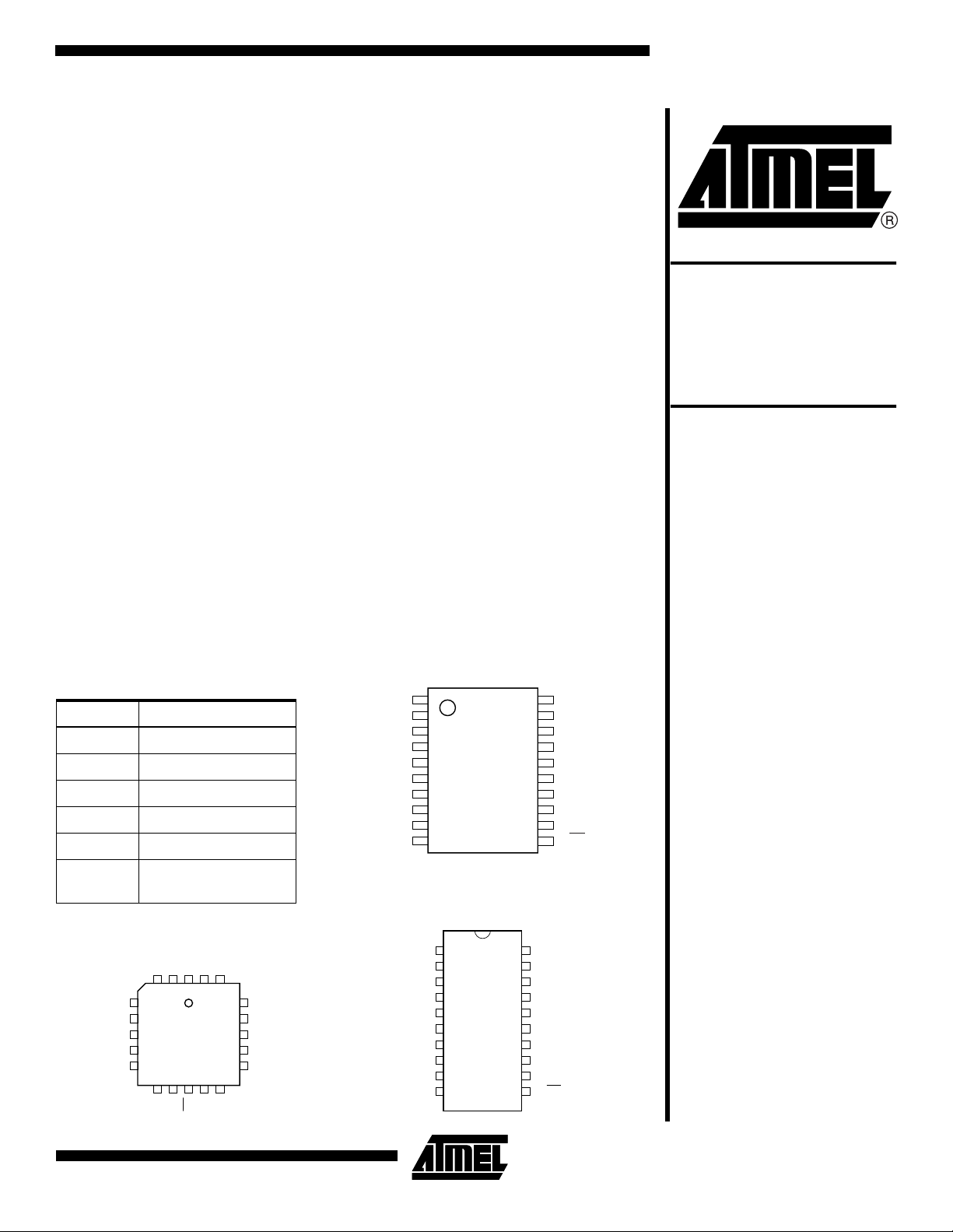
Pin Configurations
All Pinouts Top View
Pin Name Function
CLK Clock
I Logic Inputs
I/O Bidirectional Buffers
OE Output Enable
VCC (+3V to 5.5V) Supply
Programmable Powerdown Opti on
PD
I/CLK
I1
I2
PD/I3
I4
I5
I6
I7
I8
GND
PLCC
I/CLK
PD/I3
GND
1
2
3
4
5
6
7
8
9
10
I1
I2
I4
I5
I6
I7
I8
TSSOP
DIP/SOIC
1
2
3
4
5
6
7
8
9
10
20
19
18
17
16
15
14
13
12
11
20
VCC
19
I/O
18
I/O
17
I/O
16
I/O
15
I/O
14
I/O
13
I/O
12
I/O
11
I9/OE
(continued)
VCC
I/O
I/O
I/O
I/O
I/O
I/O
I/O
I/O
I9/OE
Rev. 0403G–08/99
1
Page 2
ranges are specified over the full 3.0V to 5.25V range for
industrial and commercial temperature ranges.
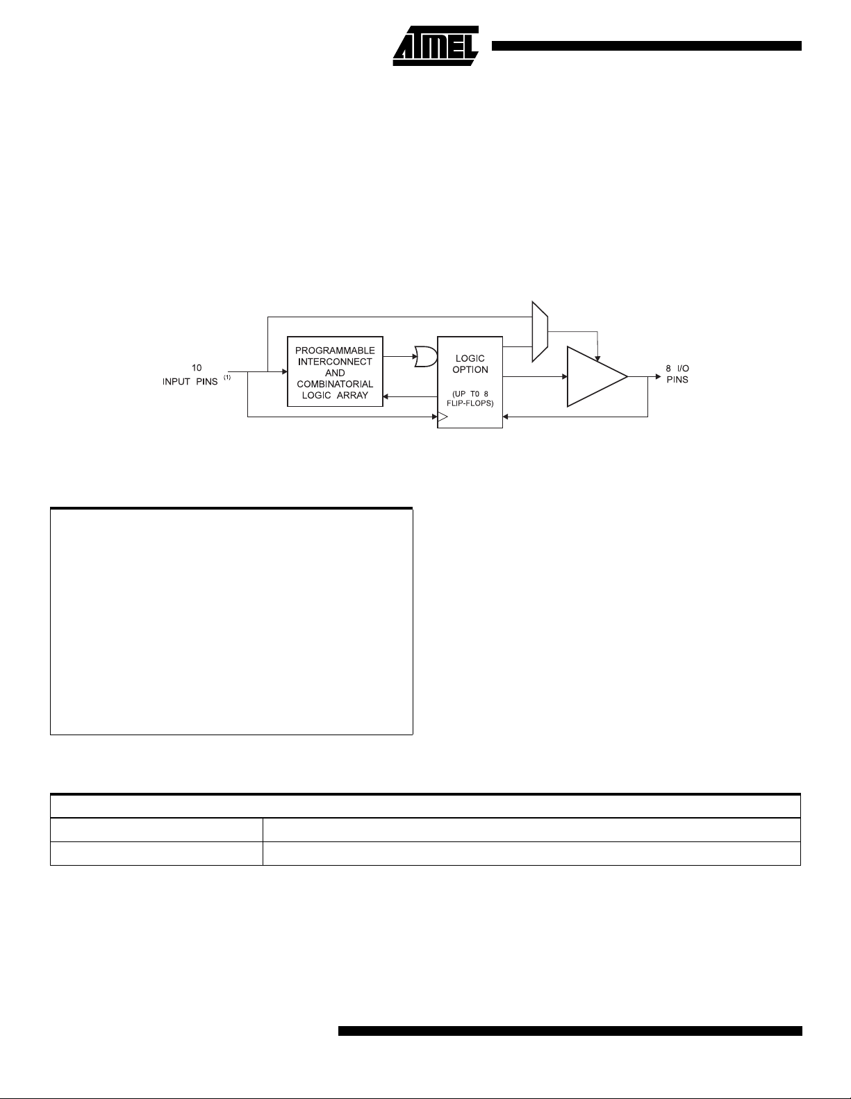
The ATF16LV8C incorpora tes a superse t of the gener ic
architectures, wh ich allows direct repl acemen t of the 16R8
family and most 20-pin combinatorial PLDs. Ei ght outputs
are each allocated eight produc t terms. Three different
modes of operation, configured automatically with software, allow highly complex logic functions to be realized.
Block Diagram
Note: 1. Includes optional PD control pin.
Absolute Maximum Ratings*
Temperature Under Bias.................................. -40°C to +85°C
Storage Temperature..................................... -65°C to +150°C
Voltage on Any Pin with
Respect to Ground .........................................-2.0V to +7.0V
Voltage on Input Pins
with Respect to Ground
During Programming.....................................-2.0V to +14.0V
Programming Voltage with
Respect to Ground .......................................-2.0V to +14.0V
(1)
(1)
(1)
The ATF16LV8C can significantly reduce total system
power, thereby enhancing system reliability and reducing
power supply costs. When pin 4 is configured as the
power-down control pin, supply current drops to less than
5µA whenever the pin is high. If the power-down feature
isn’t required for a particular application, pin 4 may be used
as a logic input. Also, the pin keeper circuits eliminate the
need for internal pu ll -up r esis to rs a lon g wi th t hei r atte nda nt
power consumption.
*NOTICE: Stresses beyond those listed under “Absolute
Maximum Ratings” may cause permanent damage to the device . This is a st ress rating only and
functional operatio n of the dev ice at th ese or an y
other conditions beyond those indicated in the
operational sections of this specification is not
implied. Exposure to absolute maximum rating
conditions for exten ded periods may af fect device
reliability.
Note: 1. Minimum voltage is -0.6V DC, which may under-
shoot to -2.0V for pulses of less than 20 ns.
Maximum output pin voltage is Vcc + 0.75V DC,
which may overshoot to 7.0V for pulses of less
than 20 ns.
DC and AC Operating Conditions
Commercial
Operating Temperature (Ambient) 0°C - 70°C
V
Power Supply 3.0V to 5.5V
CC
2
ATF16LV8C
Page 3
DC Characteristics
Symbol Parameter Condition
ATF16LV8C
(2)
Min Typ Max Units
I
I
I
I
I
V
V
V
V
I
I
IL
IH
CC1
PD
OS
IL
IH
OL
OH
OL
OH
(1)
(1)
Input or I/O Low Leakage Current 0 ≤ VIN ≤ VIL(Max) -10 µA
Input or I/O High Leakage Current 1.8 ≤ VIN ≤ V
Power Supply Current
Power Supply Current, Power-down Mode
Output Short Circuit Current
Input Low Voltage MIN < VCC < Max -0.5 0.8 V
Input High Voltage 2.0 VCC + 1 V
Output Low Voltage
Output High Voltage
Output Low Current VCC = Min 8 mA
Output High Current VCC = Min -4 mA
Note: 1. All ICC parameters measured with outputs open.
2. For DC characteristics, the test condition of V
CC
CC
15 MHz, V
= 0, V
V
IN
CC
CC,
= Max,
Outputs Open
= Max,
V
CC
= 0, V
V
IN
V
OUT
V
CC
V
CC
I
OL
V
CC
I
OH
CC
= 0.5V;
= 3V; TA = 25°C
= Min; All Outputs
= 8 mA
= Min
= -4 mA
= Max corresponds to 3.6V.
10 µA
Com.
Ind.
55
60
mA
0.1 5 µA
-150 mA
0.5 V
2.4 V
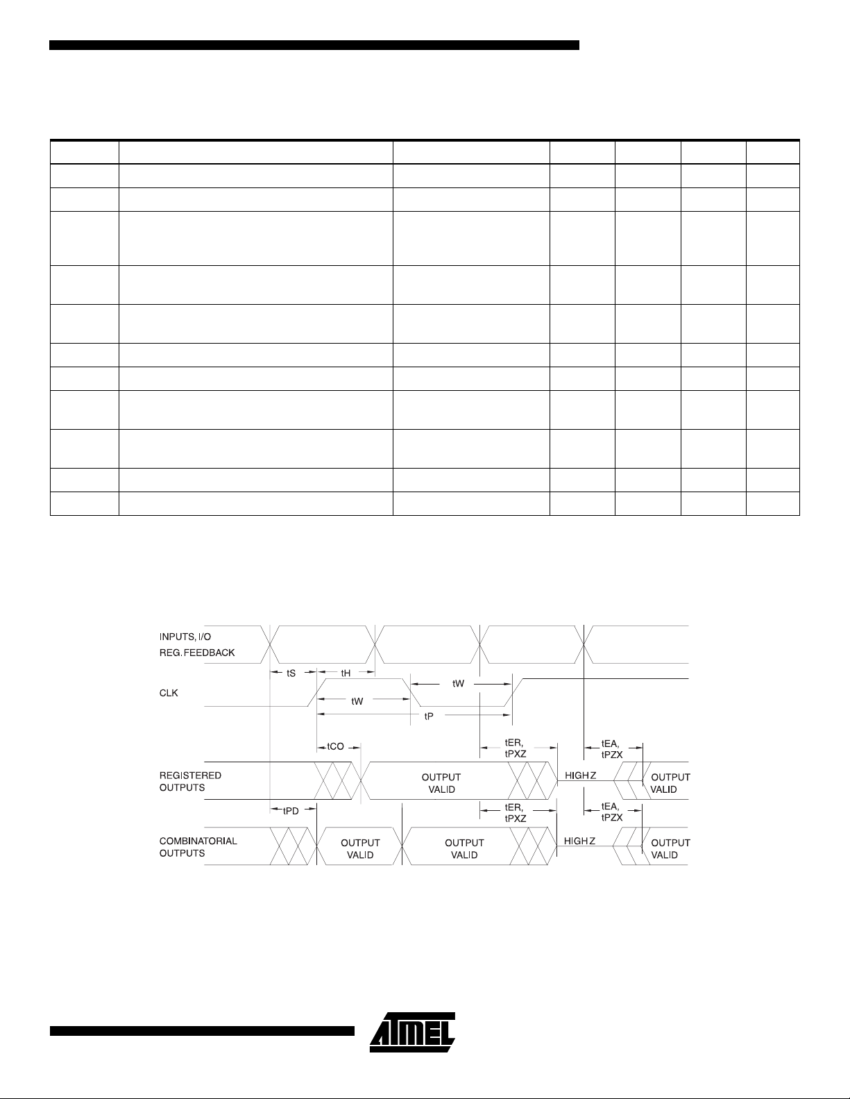
AC Waveforms
(1)
Note: 1. Timing measurement reference is 1.5V. Input AC driving levels are 0.0V and 3.0V, unless otherwise specified.
3
Page 4
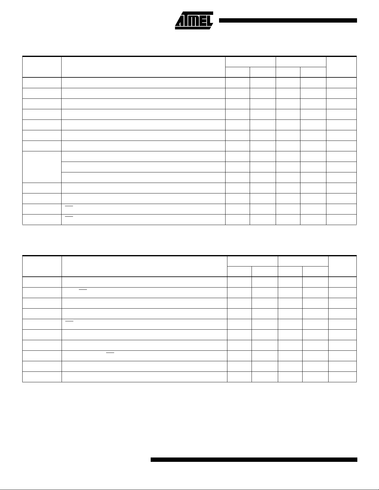
AC Characteristics
Symbol Parameter
-10 -15
UnitsMinMaxMinMax
t
PD
t
CF
t
CO
t
S
t
H
t
P
t
W
Input or Feedback to Non-Registered Output 1 10 1 15 ns
Clock to Feedback 5 8 ns
Clock to Output 2 7 2 10 ns
Input or Feedback Setup Time 7 12 ns
Input Hold Time 0 0 ns
Clock Period 12 16 ns
Clock Width 6 8 ns
External Feedback 1/(tS+ tCO) 71.4 45.5 MHz
F
t
t
t
t
MAX
EA
ER
PZX
PXZ
Internal Feedback 1/(tS + tCF)83.350MHz
No Feedback 1/(t
) 83.3 62.5 MHz
P
Input to Output Enable — Product Term 3 10 3 1 5 ns
Input to Output Disable — Product Term 2 10 2 15 ns
OE pin to Output Enable 2 8 2 15 ns
OE pin to Output Disable 1.5 8 1.5 15 ns
Power-down AC Characteristics
(1)(2)(3)
-10 -15
Symbol Parameter
t
IVDH
t
GVDH
t
CVDH
t
DHIX
t
DHGX
t
DHCX
t
DLIV
t
DLGV
t
DLCV
t
DLOV
Valid Input Before PD High 10 15 ns
Valid OE Before PD High 0 0 ns
Valid Clock Before PD High 0 0 ns
Input Don't Care After PD High 10 15 ns
OE Don't Care After PD High 10 15 ns
Clock Don't Care After PD High 10 15 ns
PD Low to Valid Input 10 15 ns
PD Low to Valid OE 25 30 ns
PD Low to Valid Clock 25 30 ns
PD Low to Valid Output 30 35 ns
Notes: 1. Output data is latched and held.
2. HI-Z ou tputs remain HI-Z.
3. Clock and input transitions are ignored.
UnitsMin Max Min Max
4
ATF16LV8C
Page 5

ATF16LV8C
Input Test Waveforms and Measurement Levels:
tR, tF < 1.5ns (10% to 90%)
Output Test Loads: Commercial
3.3V
R1 = 316
R2 = 348
Note: Similar devices are tested with slightly different loads.
These load differences may affect output signals’ delay
and slew rate. Atmel devices are tested with sufficient
margins to meet compatible devices.
Pin Capacitance
(f = 1 MHz, T = 25°C)
C
IN
C
OUT
Note: 1. Typical values for nominal supply voltage. This parameter is only sampled and is not 100% tested.
(1)
Typ Max Units Conditions
58 pFV
68 pFV
OUTPUT
PIN
CL = 35pF
= 0V
IN
= 0V
OUT
Power-up Reset
The ATF16LV8C’s registers are designed to reset during
power-up. At a point delayed slightly from V
, all registers will be re set to th e low st ate. As a r esult,
V
RST
the registered output state will always be high on power-up.
This feature is crit ical for state machine initialization.
However, due to the asynchronous nature of reset and the
uncertainty of how V
actually rises in the system, the
CC
following conditions are required:
1. The V
rise must be monotonic from below 0.7V.
CC
2. The signals from which the clock is derived must
remain stable during T
3. After T
, all input and feedback setup times must
PR
PR
.
be met before driving the clock ter m high.
crossing
CC
Parameter Description Typ Max Units
T
PR
V
RST
Power-up
Reset Time
Power-up
Reset
Voltage
600 1,000 ns
2.5 3.0 V
5
Page 6

ICC mA
SUPPLY CURRENT
VS.INPUT FREQUENCY
(VCC = 3.3V, TA = 25°C)
40.0
39.5
39.0
38.5
38.0
37.5
37.0
10 20 30 40 50 60 70 80 90 100
FREQUENCY (MHz)
IOL mA
OUTPUT SINK CURRENT
VS.OUTPUT VOLTAGE (VCC = 5V, TA = 25°C)
60
50
40
30
20
10
0
0 0.1 0.2 0.3 0.4 0.5 0.6 0.7 0.8 0.9 1.0 1.1 1.2 1.3 1.4 1.5
OUTPUT VOLTAGE (V)
NORM
ICC mA
IOL mA
NORMALIZED SUPPLY CURRENT
VS.AMBIENT TEMPERATURE
1.6
1.4
1.2
1.0
0.8
0.6
0.4
0.2
0
-5°
(VCC = 3.3V, STANDBY)
25°
AMBIENT TEMPERATURE (C)
OUTPUT SINK CURRENT
VS.SUPPLY VOLTAGE (TA = 25°C, VOL = 0.45V)
25.0
24.5
24.0
23.5
23.0
22.5
22.0
21.5
21.0
20.5
3.0 3.15 3.3 3.45 3.6
SUPPLY VOLTAGE (V)
75°
NORM
ICC mA
IOH mA
NORMALIZED SUPPLY CURRENT
VS.SUPPLY VOLTAGE
(TA = 25°C, STANDBY)
1.6
1.4
1.2
1.0
0.8
0.6
0
3.0 3.3 3.6
SUPPLY VOLTAGE (V)
OUTPUT SOURCE CURRENT
VS.SUPPLY VOLTAGE (VOH = 2.4V, TA = 25°C)
0
-2
-4
-6
-8
-10
-12
-14
-16
3.0
3.15 3.3
3.45
SUPPLY VOLTAGE (V)
3.6
6
ATF16LV8C
Page 7

ATF16LV8C
0
0.2
0.4
0.6
0.8
1.0
1.2
3.0 3.25 3.6
NORMALIZED t
PD
VS.SUPPLY VOLTAGE (TA = 25°C)
SUPPLY VOLTAGE (V)
NORM
t
PD
IOH mA
OUTPUT SOURCE CURRENT
VS.OUTPUT VOLTAGE (VCC = 5V, TA = 25°C)
0
-5
-10
-15
-20
-25
-30
0.5 1.0
1.5 2.0
2.5
OUTPUT VOLTAGE (V)
3.0 3.3
NORM
t
CO
NORM
t
S
NORMALIZED t
VS.AMBIENT TEMPERATURE (VCC = 3.3V)
1.06
1.04
1.02
1.00
0.98
0.96
0.94
0.92
0.90
0.88
-5°
AMBIENT TEMPERATURE (C)
VS.AMBIENT TEMPERATURE (VCC = 3.3V)
1.06
1.04
1.02
1.00
0.98
0.96
0.94
0.92
-5° 25°
AMBIENT TEMPERATURE (C)
25° 75°
NORMALIZED t
CO
S
75°
NORMALIZED t
VS.AMBIENT TEMPERATURE (VCC = 3.3V)
1.06
1.04
1.02
NORM
1.00
0.98
t
PD
0.96
0.94
0.92
0.90
-5°
25°
AMBIENT TEMPERATURE (C)
PD
NORM
t
H
75°
VS.AMBIENT TEMPERATURE (VCC = 3.3V)
1.2
1.0
0.8
0.6
0.4
0.2
0
-5° 25°
NORMALIZED t
H
75°
AMBIENT TEMPERATURE (C)
7
Page 8

0
0.2
0.4
0.6
0.8
1.0
1.2
3.0 3.25 3.6
NORMALIZED t
CO
VS.SUPPLY VOLTAGE (TA = 25°C)
SUPPLY VOLTAGE (V)
NORM
t
CO
0
0.2
0.4
0.6
0.8
1.0
1.2
3.0 3.25 3.6
NORMALIZED t
S
VS.SUPPLY VOLTAGE (TA = 25°C)
NORM
t
S
SUPPLY VOLTAGE (V)
0
0.2
0.4
0.6
0.8
1.0
1.2
3.0 3.25 3.6
NORMALIZED t
H
VS.SUPPLY VOLTAGE (TA = 25°C)
SUPPLY VOLTAGE (V)
NORM
t
H
INPUT
CURRENT
mA
INPUT CLAMP CURRENT
VS.INPUT VOLTAGE (TA = 25°C, VCC = 3.3V)
0
-10
-20
-30
-40
-50
-60
-70
-80
-0.1
0
-0.2 -0.3 -0.4
-0.5
-0.6 -0.7 -0.8 -0.9
INPUT VOLTAGE (V)
-1.0
INPUT
CURRENT
mA
VS.INPUT VOLTAGE (TA = 25°C, VCC = 3.3V)
35
30
25
20
15
10
5
0
-5
-10
-15
-20
0 0.5 1.5 2.5
1.0 2.0
INPUT VOLTAGE (V)
INPUT CURRENT
3.0
3.3
8
ATF16LV8C
Page 9

Ordering Information
ATF16LV8C
t
PD
(ns)
10 7 7 ATF16LV8C-10JC
15 12 10 ATF16LV8C-15JC
10 7 7 ATF16LV8C-10JI
15 12 10 ATF16LV8C-15JI
t
S
(ns)
t
CO
(ns) Ordering Code Package Operation Range
ATF16LV8C-10PC
ATF16LV8C-10SC
ATF16LV8C-10XC
ATF16LV8C-15PC
ATF16LV8C-15SC
ATF16LV8C-15XC
ATF16LV8C-10PI
ATF16LV8C-10SI
ATF16LV8C-10XI
ATF16LV8C-15PI
ATF16LV8C-15SI
ATF16LV8C-15XI
20J
20P3
20S
20X
20J
20P3
20S
20X
20J
20P3
20S
20X
20J
20P3
20S
20X
Commercial
(0°C to 70°C)
Commercial
(0°C to 70°C)
Industrial
(-40°C to 85°C)
Industrial
(-40°C to 85°C)
Using “C” Product for Industrial
To use commercial product for industrial temperature ranges, simply de-rate ICC by 15% on the “C” device. No speed
de-rating is necessary.
Package Type
20J 20-lead, Plastic J-leaded Chip Carrier (PLCC)
20P3 20-lead, 0.300" Wide, Plastic Dual Inline Package (PDIP)
20S 20-lead, 0.300" Wide, Plastic Gull-wing Small Outline (SOIC)
20X 20-lead, 4.4 mm Wide, Plastic Thin Shrink Small Outline (TSSOP)
9
Page 10

Packaging Information
20J, 20-lead, Plastic J-leaded Chip Carrier (PLCC)
Dimensions in Inches and (Millimeters)
JEDEC STANDARD MS-018 AA
20P3, 20-lead, 0.300" Wide, Plastic Dual Inline
Package (PDIP)
Dimensions in Inches and (Millimeters)
JEDEC STANDARD MS-001 AD
1.060(26.9)
.210(5.33)
SEATING
PLANE
MAX
.150(3.81)
.115(2.92)
.110(2.79)
.090(2.29)
.014(.356)
.008(.203)
.980(24.9)
.900(22.86) REF
PIN
1
.070(1.78)
.045(1.13)
.325(8.26)
.300(7.62)
0
REF
15
.430(10.92) MAX
.090(2.29)
.005(.127)
.015(.381) MIN
.022(.559)
.014(.356)
.280(7.11)
.240(6.10)
MAX
MIN
20S, 20-lead, 0.300" Wide, Plastic Gull-wing Small
Outline (SOIC)
Dimensions in Inches and (Millimeters)
0.020 (0.508)
0.013 (0.330)
0.420 (10.7)
0.299 (7.60)
0.393 (9.98)
0.012 (0.305)
0.003 (0.076)
0.291 (7.39)
0.013 (0.330)
0.009 (0.229)
0.105 (2.67)
0.092 (2.34)
PIN 1
.050 (1.27) BSC
0.513 (13.0)
0.497 (12.6)
0
REF
8
0.035 (0.889)
0.015 (0.381)
20X, 20-lead, 4.4 mm Wide, Plastic Thin Shrink
Small Outline (TSSOP)
Dimensions in Millimeters and (Inches)*
0.30(0.012)
0.18(0.007)
PIN 1 ID
0
REF
8
6.60(.260)
6.40(.252)
0.70(.028)
0.50(.020)
4.48(.176)
4.30(.169)
0.65(.0256) BSC
0.15(.006)
0.05(.002)
6.50(.256)
6.25(.246)
1.10(0.043) MAX
0.18(.007)
0.09(.003)
*Controlling dimension: millimeters.
10
ATF16LV8C
Page 11

Atmel Headquarters Atmel Operations
Corporate Headquarters
2325 Orchard Parkway
San Jose, CA 95131
TEL (408) 441- 0311
FAX (408) 487-2600
Europe
Atmel U.K., Ltd.
Coliseum Business Centre
Riverside Way
Camberley, Surrey GU15 3YL
England
TEL (44) 1276-686-677
FAX (44) 1276-686-697
Asia
Atmel Asia, Ltd.
Room 1219
Chinachem Golden Plaza
77 Mody Road Tsimhatsui
East Kowloon
Hong Kong
TEL (852) 2721 -9778
FAX (852) 2722-1369
Japan
Atmel Japan K.K.
9F, Tonetsu Shinkawa Bldg.
1-24-8 Shink awa
Chuo-ku, Tokyo 104-0033
Japan
TEL (81) 3-3523-3551
FAX (81) 3-3523-7581
Atmel Colorado Springs
1150 E. Cheyenne Mtn. Blvd.
Colorado Springs, CO 80906
TEL (719) 576-3300
FAX (719) 540-1759
Atmel Rousset
Zone Indu strie lle
13106 Rousset Cedex
France
TEL (33) 4-4253-6000
FAX (33) 4-4253-6001
Fax-on-Demand
North America:
1-(800) 292-8635
International:
1-(408) 441-0732
e-mail
literature@atmel.com
Web Site
http://www.atmel.com
BBS
1-(408) 436-4309
© Atmel Corporation 1999.
Atmel Corporation makes no warranty for the use of its products, other than those expressly contained in the Company’s standard warranty which is detailed in Atmel’s Terms and Conditions located on the Company’s web site. The Company assumes no responsibility for
any errors which may appear in this document, reserves the right to change devices or specifications detailed herein at any time without
notice, and does not make any commitment to update the information contained herein. No licenses to patents or other intellectual property of Atmel are granted by the Company in connection with the sale of Atmel products, expressly or by implication. Atmel’s products are
not authorized for use as critical components in life support devices or systems.
Marks bearing ® and/or ™ are registered trademarks and trademarks of Atmel Corporation.
Terms and product names in this document may be trademarks of others.
Printed on recycled paper.
0403G–08/99/xM
 Loading...