

Page 1
Features
• Single 2.7V - 3.6V Supply
• Dual-interface Architecture
– Dedicated Serial Interface (SPI Modes 0 and 3 Compatible)
– Dedicated Parallel I/O Interface (Optional Use)
• Page Program Operation
– Single Cycle Reprogram (Erase and Program)
– 8192 Pages (1056 Bytes/Page) Main Memory
• Supports Page and Block Erase Operations
• Two 1056-byte SRAM Data Buffers – Allows Receiving of Data
while Reprogramming the Flash Array
• Continuous Read Capability through Entire Array
– Ideal for Code Shadowing Applications
• Low-power Dissipation
– 4 mA Active Read Current Typical
– 2 µA CMOS Standby Current Typical
• 20 MHz Maximum Clock Frequency – Serial Interface
• 5 MHz Maximum Clock Frequency – Parallel Interface
• Hardware Data Protection
• Commercial and Industrial Temperature Ranges
Description
The AT45DB642 is a 2.7-volt only, dual-interface Flash memory ideally suited for a
wide variety of digital voice-, image-, program code- and data-storage applications. The
dual-interface of the AT45DB642 allows a dedicated serial interface to be connected to a
DSP and a dedicated parallel interface to be connected to a microcontroller or vice versa.
64-megabit
2.7-volt Only
Dual-interface
DataFlash
®
AT45DB642
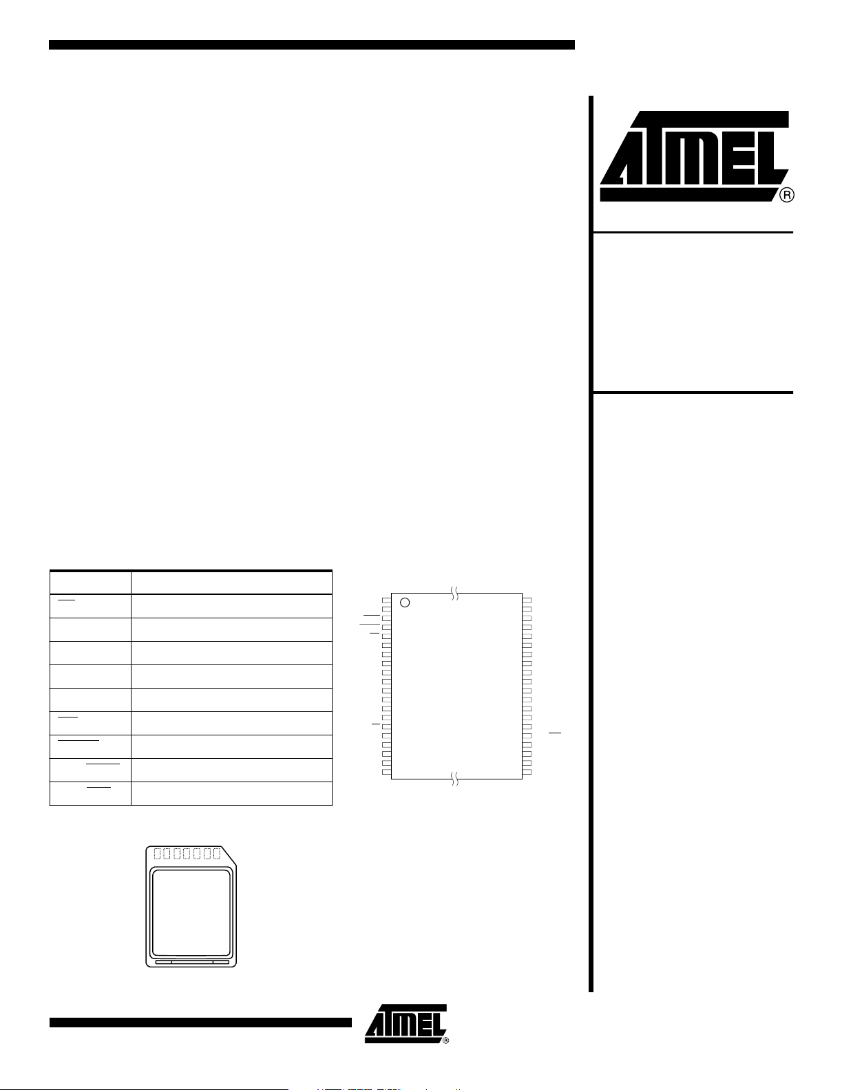
Pin Configurations
Pin Name Function
CS
SCK/CLK Serial Clock/Clock
SI Serial Input
SO Serial Output
I/O7 - I/O0 Parallel Input/Output
WP
RESET
RDY/BUSY
SER/PAR
Chip Select
Hardware Page Write Protect Pin
Chip Reset
Ready/Busy
Serial/Parallel Interface Control
DataFlash Card
7654321
(1)
TSOP Top View
Typ e 1
1
NC
2
NC
RESET
VCC
GND
SCK/CLK
SO*
3
4
5
WP
6
NC
7
NC
8
NC
9
10
11
NC
12
NC
13
NC
14
NC
15
CS
16
17
SI*
18
19
NC
20
NC
RDY/BUSY
Note: *Optional Use – See pin description
text for connection information.
NC
40
NC
39
NC
38
NC
37
NC
36
I/O7*
35
I/O6*
34
I/O5*
33
I/O4*
32
VCCP*
31
GNDP*
30
I/O3*
29
I/O2*
28
I/O1*
27
I/O0*
26
SER/PAR*
25
NC
24
NC
23
NC
22
NC
21
Note: 1. See AT45DCB008 Datasheet.
Rev. 1638F–DFLSH–09/02
1
Page 2
However, the use of either interface is purely optional. Its 69,206,016 bits of memory are organized as 8192 pages of 1056 bytes each. In addition to the main memory, the AT45DB642
also contains two SRAM data buffers of 1056 bytes each. The buffers allow receiving of data
while a page in the main memory is being reprogrammed, as well as reading or writing a continuous data stream. EEPROM emulation (bit or byte alterability) is easily handled with a selfcontained three step Read-Modify-Write operation. Unlike conventional Flash memories that
are accessed randomly with multiple address lines and a parallel interface, the DataFlash
uses either a serial interface or a parallel interface to sequentially access its data. The simple
sequential access facilitates hardware layout, increases system reliability, minimizes switching
noise, and reduces package size and active pin count. DataFlash supports SPI mode 0 and
mode 3. The device is optimized for use in many commercial and industrial applications where
high-density, low-pin count, low-voltage, and low-power are essential. The device operates at
clock frequencies up to 20 MHz with a typical active read current consumption of 4 mA.
To allow for simple in-system reprogrammability, the AT45DB642 does not require high input
voltages for programming. The device operates from a single power supply, 2.7V to 3.6V, for
both the program and read operations. The AT45DB642 is enabled through the chip select pin
(CS
) and accessed via a three-wire interface consisting of the Serial Input (SI), Serial Output
(SO), and the Serial Clock (SCK), or a parallel interface consisting of the parallel input/output
pins (I/O7 - I/O0) and the clock pin (CLK). The SCK and CLK pins are shared and provide the
same clocking input to the DataFlash.
All programming cycles are self-timed, and no separate erase cycle is required before
programming.
When the device is shipped from Atmel, the most significant page of the memory array may
not be erased. In other words, the contents of the last page may not be filled with FFH.
®
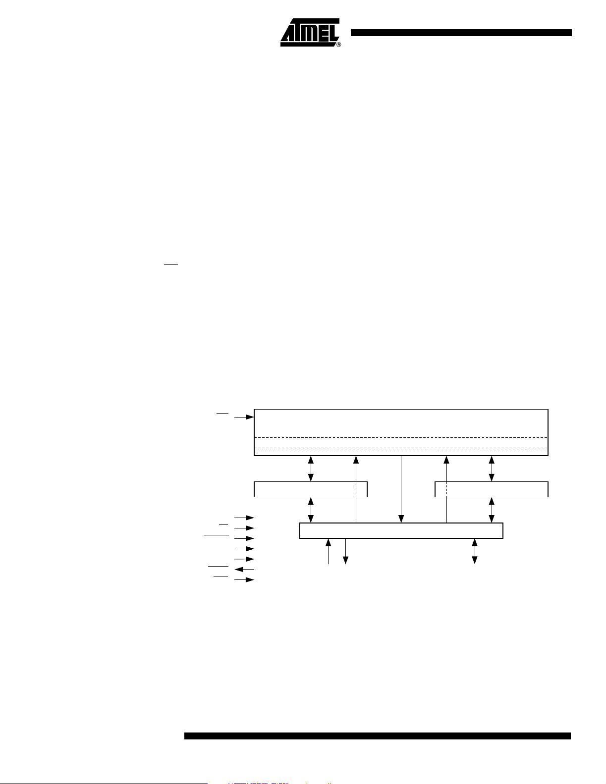
Block Diagram
Memory Array
WP
PAGE (1056 BYTES)
SCK/CLK
CS
RESET
VCC
GND
RDY/BUSY
SER/PAR
FLASH MEMORY ARRAY
I/O INTERFACE
SOSI
BUFFER 2 (1056 BYTES)BUFFER 1 (1056 BYTES)
I/O7 - I/O0
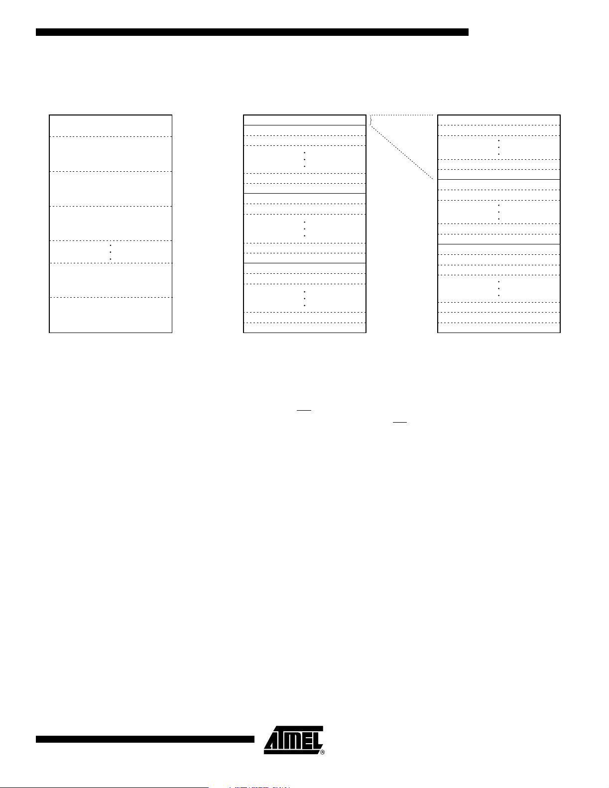
To provide optimal flexibility, the memory array of the AT45DB642 is divided into three levels
of granularity comprising of sectors, blocks and pages. The “Memory Architecture Diagram”
illustrates the breakdown of each level and details the number of pages per sector and block.
All program operations to the DataFlash occur on a page-by-page basis; however, the optional
erase operations can be performed at the block or page level.
2
AT45DB642
1638F–DFLSH–09/02
Page 3
AT45DB642
Memory Architecture Diagram
SECTOR ARCHITECTURE BLOCK ARCHITECTURE PAGE ARCHITECTURE
SECTOR 0 = 8 Pages
8448 bytes (8K + 256)
SECTOR 1 = 248 Pages
261,888 bytes (248K + 7936)
SECTOR 2 = 256 Pages
270,336 bytes (256K + 8K)
SECTOR 3 = 256 Pages
270,336 bytes (256K + 8K)
SECTOR 31 = 256 Pages
270,336 bytes (256K + 8K)
SECTOR 0
SECTOR 1
SECTOR 2
BLOCK 0
BLOCK 1
BLOCK 2
BLOCK 30
BLOCK 31
BLOCK 32
BLOCK 33
BLOCK 62
BLOCK 63
BLOCK 64
BLOCK 65
8 Pages
BLOCK 0
BLOCK 1
PAGE 0
PAGE 1
PAGE 6
PAGE 7
PAGE 8
PAGE 9
PAGE 14
PAGE 15
PAGE 16
PAGE 17
PAGE 18
SECTOR 32 = 256 Pages
270,336 bytes (256K + 8K)
Device Operation
BLOCK 1022
BLOCK 1023
Block = 8448 bytes
(8K + 256)
The device operation is controlled by instructions from the host processor. The list of instructions and their associated opcodes are contained in Tables 1 through 4. A valid instruction
starts with the falling edge of CS
buffer or main memory address location. While the CS
followed by the appropriate 8-bit opcode and the desired
pin is low, toggling the SCK/CLK pin
PAGE 8189
PAGE 8190
PAGE 8191
Page = 1056 bytes
(1K + 32)
controls the loading of the opcode and the desired buffer or main memory address location
through either the SI (serial input) pin or the parallel input pins (I/O7 - I/O0). All instructions,
addresses, and data are transferred with the most significant bit (MSB) first.
Buffer addressing is referenced in the datasheet using the terminology BFA10 - BFA0 to
denote the 11 address bits required to designate a byte address within a buffer. Main memory
addressing is referenced using the terminology PA12 - PA0 and BA10 - BA0, where PA12 -
PA0 denotes the 13 address bits required to designate a page address and BA10 - BA0
denotes the 11 address bits required to designate a byte address within the page.
Read Commands By specifying the appropriate opcode, data can be read from the main memory or from either
one of the two SRAM data buffers. The DataFlash supports two categories of read modes in
relation to the SCK/CLK signal. The differences between the modes are in respect to the inactive state of the SCK/CLK signal as well as which clock cycle data will begin to be output. The
two categories, which are comprised of four modes total, are defined as Inactive Clock Polarity
Low or Inactive Clock Polarity High and SPI Mode 0 or SPI Mode 3. A separate opcode (refer
to Table 1 for a complete list) is used to select which category will be used for reading. Please
refer to the “Detailed Bit-level Read Timing” diagrams in this datasheet for details on the clock
cycle sequences for each mode.
1638F–DFLSH–09/02
3
Page 4

CONTINUOUS ARRAY READ: By supplying an initial starting address for the main memory
array, the Continuous Array Read command can be utilized to sequentially read a continuous
stream of data from the device by simply providing a clock signal; no additional addressing
information or control signals need to be provided. The DataFlash incorporates an internal
address counter that will automatically increment on every clock cycle, allowing one continuous read operation without the need of additional address sequences. To perform a
continuous read, an opcode of 68H or E8H must be clocked into the device followed by three
address bytes (which comprise the 24-bit page and byte address sequence) and a series of
don’t care bytes (four don’t care bytes if using the serial interface or 60 don’t care bytes if
using the parallel interface). The first 13 bits (PA12 - PA0) of the 24-bit (three byte) address
sequence specify which page of the main memory array to read, and the last 11 bits (BA10 -
BA0) of the 24-bit address sequence specify the starting byte address within the page. The
four or 60 don’t care bytes that follow the three address bytes are needed to initialize the read
operation. Following the don’t care bytes, additional clock pulses on the SCK/CLK pin will
result in data being output on either the SO (serial output) pin or the parallel output pins (I/O7I/O0).
The CS
care bytes, and the reading of data. When the end of a page in main memory is reached during a Continuous Array Read, the device will continue reading at the beginning of the next
page with no delays incurred during the page boundary crossover (the crossover from the end
of one page to the beginning of the next page). When the last bit (or byte if using the parallel
interface mode) in the main memory array has been read, the device will continue reading
back at the beginning of the first page of memory. As with crossing over page boundaries, no
delays will be incurred when wrapping around from the end of the array to the beginning of the
array.
A low-to-high transition on the CS
pins (SO or I/O7-I/O0). The maximum SCK/CLK frequency allowable for the Continuous Array
Read is defined by the f
buffers and leaves the contents of the buffers unchanged.
BURST ARRAY READ WITH SYNCHRONOUS DELAY: The Burst Array Read with Synchronous Delay functions very similarly to the Continuous Array Read operation but allows much
higher read throughputs by utilizing faster clock frequencies. It incorporates a synchronous
delay (through the use of don't care clock cycles) when crossing over page boundaries. To
perform a Burst Array Read with Synchronous Delay, an opcode of 69H or E9H must be
clocked into the device followed by three address bytes (which comprise the 24-bit page and
byte address sequence) and a series of don't care bytes (four don't care bytes if using the
serial interface or 60 don't care bytes if using the parallel interface). The first 13 bits (PA12PA0) of the 24-bit (three byte) address sequence specify which page of the main memory
array to read, and the last 11 bits (BA10-BA0) of the 24-bit address sequence specify the starting byte address within the page. The don't care bytes that follow the three address bytes are
needed to initialize the read operation. Following the don't care bytes, additional clock pulses
on the SCK/CLK pin will result in data being output on either the SO pin or the I/O7-I/O0 pins.
pin must remain low during the loading of the opcode, the address bytes, the don’t
pin will terminate the read operation and tri-state the output
specification. The Continuous Array Read bypasses both data
CAR
4
AT45DB642
1638F–DFLSH–09/02
Page 5

AT45DB642
As with the Continuous Array Read, the CS pin must remain low during the loading of the
opcode, the address bytes, the don't care bytes, and the reading of data. During a Burst Array
Read with Synchronous Delay, when the end of a page in main memory is reached (the last bit
or the last byte of the page has been clocked out), the system must send an additional 32
don't care clock cycles before the first bit (or byte if using the parallel interface mode) of the
next page can be read out. These 32 don't care clock cycles are necessary to allow the device
enough time to cross over the burst read boundary (the crossover from the end of one page to
the beginning of the next page). By utilizing the 32 don't care clock cycles, the system does
not need to delay the SCK/CLK signal to the device which allows synchronous operation when
reading multiple pages of the memory array. Please see the detailed read timing waveforms
for illustrations (beginning on page 21) on which clock cycle data will actually begin to be
output.
When the last bit (or byte in the parallel interface mode) in the main memory array has been
read, the device will continue reading back at the beginning of the first page of memory. The
transition from the last bit (or byte when using the parallel interface) of the array back to the
beginning of the array is also considered a burst read boundary. Therefore, the system must
send 32 don't care clock cycles before the first bit (or byte if using the parallel interface mode)
of the memory array can be read.
A low-to-high transition on the CS
pins (SO or I/O7-I/O0). The maximum SCK/CLK frequency allowable for the Burst Array Read
with Synchronous Delay is defined by the f
chronous Delay bypasses both data buffers and leaves the contents of the buffers unchanged.
MAIN MEMORY PAGE READ: A main memory page read allows the user to read data
directly from any one of the 8192 pages in the main memory, bypassing both of the data buffers and leaving the contents of the buffers unchanged. To start a page read, an opcode of 52H
or D2H must be clocked into the device followed by three address bytes (which comprise the
24-bit page and byte address sequence) and a series of don’t care bytes (four don’tcarebytes
if using the serial interface or 60 don’t care bytes if the using parallel interface). The first 13
bits (PA12 - PA0) of the 24-bit (three-byte) address sequence specify the page in main memory to be read, and the last 11 bits (BA10 - BA0) of the 24-bit address sequence specify the
starting byte address within that page. The four or 60 don’t care bytes that follow the three
address bytes are sent to initialize the read operation. Following the don’tcarebytes,additional pulses on SCK/CLK result in data being output on either the SO (serial output) pin or the
parallel output pins (I/O7 - I/O0). The CS
opcode, the address bytes, the don’t care bytes, and the reading of data. When the end of a
page in main memory is reached, the device will continue reading back at the beginning of the
same page. A low-to-high transition on the CS
state the output pins (SO or I/O7 - I/O0).
BUFFER READ: Data can be read from either one of the two buffers, using different opcodes
to specify which buffer to read from. An opcode of 54H or D4H is used to read data from buffer
1, and an opcode of 56H or D6H is used to read data from buffer 2. To perform a buffer read,
the opcode must be clocked into the device followed by three address bytes comprised of 13
don’t care bits and 11 buffer address bits (BFA10 - BFA0). Following the three address bytes,
an additional don’t care byte must be clocked in to initialize the read operation. Since the
buffer size is 1056 bytes, 11 buffer address bits are required to specify the first byte of data to
be read from the buffer. The CS
address bytes, the don’t care bytes, and the reading of data. When the end of a buffer is
reached, the device will continue reading back at the beginning of the buffer. A low-to-high
transition on the CS
I/O7 - I/O0).
pin will terminate the read operation and tri-state the output pins (SO or
pin will terminate the read operation and tri-state the output
specification. The Burst Array Read with Syn-
BARSD
pin must remain low during the loading of the
pin will terminate the read operation and tri-
pin must remain low during the loading of the opcode, the
1638F–DFLSH–09/02
5
Page 6
STATUS REGISTER READ: The status register can be used to determine the device’s
ready/busy status, the result of a Main Memory Page to Buffer Compare operation, or the
device density. To read the status register, an opcode of 57H or D7H must be loaded into the
device. After the opcode is clocked in, the 1-byte status register will be clocked out on the output pins (SO or I/O7 - I/O0), starting with the next clock cycle. When using the serial interface,
the data in the status register, starting with the MSB (bit 7), will be clocked out on the SO pin
during the next eight clock cycles.
The five most-significant bits of the status register will contain device information, while the
remaining three least-significant bits are reserved for future use and will have undefined values. After the one byte of the status register has been clocked out, the sequence will repeat
itself (as long as CS
ter is constantly updated, so each repeating sequence will output new data.
Ready/busy status is indicated using bit 7 of the status register. If bit 7 is a 1, then the device
is not busy and is ready to accept the next command. If bit 7 is a 0, then the device is in a busy
state. The user can continuously poll bit 7 of the status register by stopping SCK/CLK at a low
level once bit 7 has been output on the SO or I/O7 pin. The status of bit 7 will continue to be
output on the SO or I/O7 pin, and once the device is no longer busy, the state of the SO or
I/O7 pin will change from 0 to 1. There are eight operations that can cause the device to be in
a busy state: Main Memory Page to Buffer Transfer, Main Memory Page to Buffer Compare,
Buffer to Main Memory Page Program with Built-in Erase, Buffer to Main Memory Page Program without Built-in Erase, Page Erase, Block Erase, Main Memory Page Program, and Auto
Page Rewrite.
The result of the most recent Main Memory Page to Buffer Compare operation is indicated
using bit 6 of the status register. If bit 6 is a 0, then the data in the main memory page matches
the data in the buffer. If bit 6 is a 1, then at least one bit of the data in the main memory page
does not match the data in the buffer.
remains low and SCK/CLK is being toggled). The data in the status regis-
Program and Erase Commands
The device density is indicated using bits 5, 4, 3 and 2 of the status register. For the
AT45DB642, the four bits are logical “1”s. The decimal value of these four binary bits does not
equate to the device density; the four bits represent a combinational code relating to differing
densities of DataFlash devices, allowing a total of sixteen different density configurations.
Status Register Format
Bit 7 Bit 6 Bit 5 Bit 4 Bit 3 Bit 2 Bit 1 Bit 0
RDY/BUSY
BUFFER WRITE: Data can be clocked in from the input pins (SI or I/O7 - I/O0) into either
buffer 1 or buffer 2. To load data into either buffer, a 1-byte opcode, 84H for buffer 1 or 87H for
buffer 2, must be clocked into the device, followed by three address bytes comprised of 13
don’t care bits and 11 buffer address bits (BFA10 - BFA0). The 11 buffer address bits specify
the first byte in the buffer to be written. After the last address byte has been clocked into the
device, data can then be clocked in on subsequent clock cycles. If the end of the data buffer is
reached, the device will wrap around back to the beginning of the buffer. Data will continue to
be loaded into the buffer until a low-to-high transition is detected on the CS
COMP1111XX
pin.
6
AT45DB642
1638F–DFLSH–09/02
Page 7

AT45DB642
BUFFER TO MAIN MEMORY PAGE PROGRAM WITH BUILT-IN ERASE: Data written into
either buffer 1 or buffer 2 can be programmed into the main memory. A 1-byte opcode, 83H for
buffer 1 or 86H for buffer 2, must be clocked into the device followed by three address bytes
consisting of 13 page address bits (PA12 - PA0) that specify the page in the main memory to
be written and 11 don’t care bits. When a low-to-high transition occurs on the CS
will first erase the selected page in main memory (the erased state is a logical 1) and then program the data stored in the buffer into the specified page in main memory. Both the erase and
the programming of the page are internally self-timed and should take place in a maximum
time of t
. During this time, the status register and the RDY/BUSY pin will indicate that the
EP
part is busy.
BUFFER TO MAIN MEMORY PAGE PROGRAM WITHOUT BUILT-IN ERASE: A previouslyerased page within main memory can be programmed with the contents of either buffer 1 or
buffer 2. A 1-byte opcode, 88H for buffer 1 or 89H for buffer 2, must be clocked into the device
followed by three address bytes consisting of 13 page address bits (PA12 - PA0) that specify
the page in the main memory to be written and 11 don’t care bits. When a low-to-high transition occurs on the CS
pin, the part will program the data stored in the buffer into the specified
page in the main memory. It is necessary that the page in main memory that is being programmed has been previously erased using one of the optional erase commands (Page Erase
or Block Erase). The programming of the page is internally self-timed and should take place in
a maximum time of t
. During this time, the status register and the RDY/BUSY pin will indicate
P
that the part is busy.
pin, the part
Successive page programming operations, without doing a page erase, are not recommended. In other words, changing bytes within a page from a “1” to a “0” during multiple page
programming operations without erasing that page is not recommended.
PAGE ERASE: The optional Page Erase command can be used to individually erase any
page in the main memory array allowing the Buffer to Main Memory Page Program without
Built-in Erase command to be utilized at a later time. To perform a page erase, an opcode of
81H must be loaded into the device, followed by three address bytes comprised of 13 page
address bits (PA12 - PA0) and 11 don’t care bits. The 13 page address bits are used to specify which page of the memory array is to be erased. When a low-to-high transition occurs on
the CS
operation is internally self-timed and should take place in a maximum time of t
time, the status register and the RDY/BUSY
pin, the part will erase the selected page (the erased state is a logical 1). The erase
. During this
PE
pin will indicate that the part is busy.
BLOCK ERASE: A block of eight pages can be erased at one time allowing the Buffer to Main
Memory Page Program without Built-in Erase command to be utilized to reduce programming
times when writing large amounts of data to the device. To perform a block erase, an opcode
of 50H must be loaded into the device, followed by three address bytes comprised of 10 page
address bits (PA12 -PA3) and 14 don’t care bits. The 10 page address bits are used to specify
which block of eight pages is to be erased. When a low-to-high transition occurs on the CS
pin, the part will erase the selected block of eight pages. The erase operation is internally selftimed and should take place in a maximum time of t
the RDY/BUSY
pin will indicate that the part is busy.
. During this time, the status register and
BE
1638F–DFLSH–09/02
7
Page 8

Block Erase Addressing
PA12 PA11 PA10 PA9 PA8 PA7 PA6 PA5 PA4 PA3 PA2 PA1 PA0 Block
0 0 0 0000000XXX 0
0 0 0 0000001XXX 1
0 0 0 0000010XXX 2
0 0 0 0000011XXX 3
•
•
•
1 1 1 1111100XXX1020
1 1 1 1111101XXX1021
1 1 1 1111110XXX1022
1 1 1 1111111XXX1023
•
•
•
•
•
•
•
•
•
•
•
•
•
•
•
•
•
•
•
•
•
•
•
•
•
•
•
•
•
•
•
•
•
•
•
•
MAIN MEMORY PAGE PROGRAM THROUGH BUFFER: This operation is a combination of
the Buffer Write and Buffer to Main Memory Page Program with Built-in Erase operations.
Data is first clocked into buffer 1 or buffer 2 from the input pins (SI or I/O7 - I/O0) and then programmed into a specified page in the main memory. A 1-byte opcode, 82H for buffer 1 or 85H
for buffer 2, must first be clocked into the device, followed by three address bytes. The
address bytes are comprised of 13 page address bits (PA12 - PA0) that select the page in the
main memory where data is to be written, and 11 buffer address bits (BFA10 - BFA0) that
select the first byte in the buffer to be written. After all address bytes are clocked in, the part
will take data from the input pins and store it in the specified data buffer. If the end of the buffer
is reached, the device will wrap around back to the beginning of the buffer. When there is a
low-to-high transition on the CS
pin, the part will first erase the selected page in main memory
to all 1s and then program the data stored in the buffer into that memory page. Both the erase
and the programming of the page are internally self-timed and should take place in a maximum time of t
. During this time, the status register and the RDY/BUSY pin will indicate that
EP
the part is busy.
•
•
•
Additional Commands
8
AT45DB642
MAIN MEMORY PAGE TO BUFFER TRANSFER: A page of data can be transferred from the
main memory to either buffer 1 or buffer 2. To start the operation, a 1-byte opcode, 53H for
buffer 1 and 55H for buffer 2, must be clocked into the device, followed by three address bytes
comprised of 13 page address bits (PA12 - PA0), which specify the page in main memory that
is to be transferred, and 11 don’tcarebits.TheCS
pin must be low while toggling the
SCK/CLK pin to load the opcode and the address bytes from the input pins (SI or I/O7 - I/O0).
The transfer of the page of data from the main memory to the buffer will begin when the CS
transitions from a low to a high state. During the transfer of a page of data (t
register can be read or the RDY/BUSY
can be monitored to determine whether the transfer
), the status
XFR
pin
has been completed.
1638F–DFLSH–09/02
Page 9

AT45DB642
MAIN MEMORY PAGE TO BUFFER COMPARE: A page of data in main memory can be
compared to the data in buffer 1 or buffer 2. To initiate the operation, a 1-byte opcode, 60H for
buffer 1 and 61H for buffer 2, must be clocked into the device, followed by three address bytes
consisting of 13 page address bits (PA12 - PA0) that specify the page in the main memory that
is to be compared to the buffer, and 11 don’tcarebits.TheCS
the SCK/CLK pin to load the opcode and the address bytes from the input pins (SI or I/O7 -
I/O0). On the low-to-high transition of the CS
page will be compared with the 1056 bytes in buffer 1 or buffer 2. During this time (t
status register and the RDY/BUSY
compare operation, bit 6 of the status register is updated with the result of the compare.
AUTO PAGE REWRITE: This mode is only needed if multiple bytes within a page or multiple
pages of data are modified in a random fashion. This mode is a combination of two operations:
Main Memory Page to Buffer Transfer and Buffer to Main Memory Page Program with Built-in
Erase. A page of data is first transferred from the main memory to buffer 1 or buffer 2, and
then the same data (from buffer 1 or buffer 2) is programmed back into its original page of
main memory. To start the rewrite operation, a 1-byte opcode, 58H for buffer 1 or 59H for
buffer 2, must be clocked into the device, followed by three address bytes comprised of 13
page address bits (PA12 - PA0) that specify the page in main memory to be rewritten and 11
don’t care bits. When a low-to-high transition occurs on the CS
data from the page in main memory to a buffer and then program the data from the buffer back
into same page of main memory. The operation is internally self-timed and should take place
in a maximum time of t
cate that the part is busy.
. During this time, the status register and the RDY/BUSY pin will indi-
EP
pin will indicate that the part is busy. On completion of the
pin, the 1056 bytes in the selected main memory
pin must be low while toggling
), the
XFR
pin, the part will first transfer
Operation Mode Summary
If a sector is programmed or reprogrammed sequentially page by page, then the programming
algorithm shown in Figure 1 (page 33) is recommended. Otherwise, if multiple bytes in a page
or several pages are programmed randomly in a sector, then the programming algorithm
shown in Figure 2 (page 34) is recommended. Each page within a sector must be
updated/rewritten at least once within every 10,000 cumulative page erase/program operations in that sector.
The modes described can be separated into two groups – modes that make use of the Flash
memory array (Group A) and modes that do not make use of the Flash memory array
(Group B).
Group A modes consist of:
1. Main Memory Page to Buffer 1 (or 2) Transfer
2. Main Memory Page to Buffer 1 (or 2) Compare
3. Buffer 1 (or 2) to Main Memory Page Program with Built-in Erase
4. Buffer 1 (or 2) to Main Memory Page Program without Built-in Erase
5. Page Erase
6. Block Erase
7. Main Memory Page Program through Buffer
8. Auto Page Rewrite
9. Group B modes consist of:
10. Buffer 1 (or 2) Read
11. Buffer 1 (or 2) Write
12. Status Register Read
1638F–DFLSH–09/02
If a Group A mode is in progress (not fully completed), then another mode in Group A should
not be started. However, during this time in which a Group A mode is in progress, modes in
Group B can be started.
9
Page 10

This gives the DataFlash the ability to virtually accommodate a continuous data stream. While
data is being programmed into main memory from buffer 1, data can be loaded into buffer 2
(or vice versa). See application note AN-4 (“Using Atmel’s Serial DataFlash”) for more details.
Pin Descriptions SERIAL/PARALLEL INTERFACE CONTROL (SER/PAR): The DataFlash may be configured
to utilize either its serial port or parallel port through the use of the serial/parallel control pin
(SER/PAR
and parallel modes offered on the same device. When the SER/PAR
port (SI and SO) of the DataFlash will be used for all data transfers, and the parallel port
(I/O7 - I/O0) will be in a high impedance state. Any data presented on the parallel port while
SER/PAR
used for all data transfers, and the SO pin of the serial port will be in a high impedance state.
While SER/PAR
the serial port and parallel port can be done at anytime provided the following conditions are
met: 1) CS
(SER/PAR hold time) and T
Having both a serial port and a parallel port on the DataFlash allows the device to reside on
two buses that can be connected to different processors. The advantage of switching between
the serial and parallel port is that while an internally self-timed operation such as an erase or
program operation is started with either port, a simultaneous operation such as a buffer read
or buffer write can be started utilizing the other port.
). The Dual Interface offers more flexibility in a system design with both the serial
pin is held high, the serial
is held high will be ignored. When the SER/PAR is held low, the parallel port will be
is low, any data presented on the SI pin will be ignored. Switching between
should be held high during the switching between the two modes. 2) T
(SER/PAR Setup time) requirements should be followed.
SPS
SPH
The SER/PAR
then connection of the SER/PAR
connected or if the SER/PAR
pins (I/O7-I/O0), the VCCP pin, and the GNDP pin should be treated as “don’t connects.”
SERIAL INPUT (SI): The SI pin is an input-only pin and is used to shift data serially into the
device. The SI pin is used for all data input, including opcodes and address sequences. If the
SER/PAR
SERIAL OUTPUT (SO): The SO pin is an output-only pin and is used to shift data serially out
from the device. If the SER/PAR
connect”.
PARALLEL INPUT/OUTPUT (I/O7-I/O0): The I/O7-I/O0 pins are bidirectional and used to
clock data into and out of the device. The I/O7-I/O0 pins are used for all data input, including
opcodes and address sequences. The use of these pins is optional, and the pins should be
treated as “don’t connects” if the SER/PAR
always driven high externally.
SERIAL CLOCK/CLOCK (SCK/CLK): The SCK/CLK pin is an input-only pin and is used to
control the flow of data to and from the DataFlash. Data is always clocked into the device on
the rising edge of SCK/CLK and clocked out of the device on the falling edge of SCK/CLK.
CHIP SELECT (CS
not selected, data will not be accepted on the input pins (SI or I/O7-I/O0), and the output pins
(SO or I/O7-I/O0) will remain in a high impedance state. A high-to-low transition on the CS
is required to start an operation, and a low-to-high transition on the CS
an operation.
pin is internally pulled high; therefore, if the parallel port is never to be used,
pin is not necessary. In addition, if the SER/PAR pin is not
pin is always driven high externally, then the parallel input/output
pin is always driven low, then the SI pin should be a “don’t connect”.
pin is always driven low, then the SO pin should be a “don’t
pin is not connected or if the SER/PAR pin is
): The DataFlash is selected when the CS pin is low. When the device is
pin
pinisrequiredtoend
10
HARDWARE PAGE WRITE PROTECT: If the WP
0 and 1) of the main memory cannot be reprogrammed. The only way to reprogram the first
256 pages is to first drive the protect pin high and then use the program commands previously
mentioned. The WP
nection of the WP
recommended that the WP
AT45DB642
pin is held low, the first 256 pages (sectors
pin is internally pulled high; therefore, in low pin count applications, con-
pin is not necessary if this pin and feature will not be utilized. However, it is
pin be driven high externally whenever possible.
1638F–DFLSH–09/02
Page 11

AT45DB642
RESET: Alowstateontheresetpin(RESET) will terminate the operation in progress and
reset the internal state machine to an idle state. The device will remain in the reset condition
as long as a low level is present on the RESET
RESET
The device incorporates an internal power-on reset circuit, so there are no restrictions on the
RESET
fore, in low pin count applications, connection of the RESET
feature will not be utilized. However, it is recommended that the RESET
externally whenever possible.
pin is brought back to a high level.
pin during power-on sequences. The RESET pin is also internally pulled high; there-
pin. Normal operation can resume once the
pin is not necessary if this pin and
pinbedrivenhigh
Power-on/Reset State
System Considerations
READY/BUSY
internally self-timed operation. This pin, which is normally in a high state (through an external
pull-up resistor), will be pulled low during programming/erase operations, compare operations,
and page-to-buffer transfers.
The busy status indicates that the Flash memory array and one of the buffers cannot be
accessed; read and write operations to the other buffer can still be performed.
PARALLEL PORT SUPPLY VOLTAGE (VCCP AND GNDP): The VCCP and GNDP pins are
used to supply power for the parallel input/output pins (I/O7-I/O0). The VCCP and GNDP pins
need to be used if the parallel port is to be utilized; however, these pins should be treated as
“don’t connects” if the SER/PAR
high externally.
When power is first applied to the device, or when recovering from a reset condition, the
device will default to SPI Mode 3 or Inactive Clock Polarity High. In addition, the output pins
(SO or I/O7 - I/O0) will be in a high impedance state, and a high-to-low transition on the CS
will be required to start a valid instruction. The SPI mode or the clock polarity mode will be
automatically selected on every falling edge of CS
The SPI interface is controlled by the serial clock SCK, serial input SI and chip select CS pins.
The sequential 8-bit parallel interface is controlled by the clock CLK, 8 I/Os and chip select CS
pins. These signals must rise and fall monotonically and be free from noise. Excessive noise
or ringing on these pins can be misinterpreted as multiple edges and cause improper operation of the device. The PC board traces must be kept to a minimum distance or appropriately
terminated to ensure proper operation. If necessary, decoupling capacitors can be added on
these pins to provide filtering against noise glitches.
: This open drain output pin will be driven low when the device is busy in an
pin is not connected or if the SER/PAR pin is always driven
pin
by sampling the inactive Clock State.
1638F–DFLSH–09/02
As system complexity continues to increase, voltage regulation is becoming more important. A
key element of any voltage regulation scheme is its current sourcing capability. Like all Flash
memories, the peak current for DataFlash occur during the programming and erase operation.
The regulator needs to supply this peak current requirement. An under specified regulator can
cause current starvation. Besides increasing system noise, current starvation during programming or erase can lead to improper operation and possible data corruption.
11
Page 12
Table 1 . Read Commands
Command SCK/CLK Mode Opcode
Continuous Array Read
Burst Array Read with Synchronous Delay
Main Memory Page Read
Buffer 1 Read
Buffer 2 Read
Status Register Read
Inactive Clock Polarity Low or High 68H
SPI Mode 0 or 3 E8H
Inactive Clock Polarity Low or High 69H
SPI Mode 0 or 3 E9H
Inactive Clock Polarity Low or High 52H
SPI Mode 0 or 3 D2H
Inactive Clock Polarity Low or High 54H
SPI Mode 0 or 3 D4H
Inactive Clock Polarity Low or High 56H
SPI Mode 0 or 3 D6H
Inactive Clock Polarity Low or High 57H
SPI Mode 0 or 3 D7H
Table 2 . Program and Erase Commands
Command SCK/CLK Mode Opcode
Buffer 1 Write Any 84H
Buffer 2 Write Any 87H
Buffer 1 to Main Memor y Page Program with Built-in Erase Any 83H
Buffer 2 to Main Memor y Page Program with Built-in Erase Any 86H
Buffer 1 to Main Memor y Page Program without Built-in Erase Any 88H
Buffer 2 to Main Memor y Page Program without Built-in Erase Any 89H
Page Erase Any 81H
Block Erase Any 50H
Main Memory Page Program Through Buffer 1 Any 82H
Main Memory Page Program Through Buffer 2 Any 85H
Table 3 . Additional Commands
Command SCK/CLK Mode Opcode
Main Memory Page to Buffer 1 Transfer Any 53H
Main Memory Page to Buffer 2 Transfer Any 55H
Main Memory Page to Buffer 1 Compare Any 60H
Main Memory Page to Buffer 2 Compare Any 61H
Auto Page Rewrite Through Buffer 1 Any 58H
Auto Page Rewrite Through Buffer 2 Any 59H
Note: In Tables 2 and 3, an SCK/CLK mode designation of “Any” denotes any one of the four modes of operation (Inactive Clock
Polarity Low, Inactive Clock Polarity High, SPI Mode 0, or SPI Mode 3).
12
AT45DB642
1638F–DFLSH–09/02
Page 13

AT45DB642
PA12
PA11
PA10
PA9
PA8
PA7
PA6
PA5
BA1
BA0
Table 4. Detailed Bit-level Addressing Sequence
Address Byte Address Byte Address Byte
Additional
Don’t Care
Opcode Opcode
50H 01010000PPPPPPPPPPxxxxxxxxxxxxxx N/A
52H 01010010PPPPPPPPPPPPPBBBBBBBBBBB
53H 01010011PPPPPPPPPPPPPxxxxxxxxxxx N/A
54H 01010100xxxxxxxxxxxxxBBBBBBBBBBB 1Byte
55H 01010101PPPPPPPPPPPPPxxxxxxxxxxx N/A
56H 01010110xxxxxxxxxxxxxBBBBBBBBBBB 1Byte
57H 01010111
58H 01011000PPPPPPPPPPPPPxxxxxxxxxxx N/A
59H 01011001PPPPPPPPPPPPPxxxxxxxxxxx N/A
60H 01100000PPPPPPPPPPPPPxxxxxxxxxxx N/A
61H 01100001PPPPPPPPPPPPPxxxxxxxxxxx N/A
68H 01101000PPPPPPPPPPPPPBBBBBBBBBBB
69H 01101001PPPPPPPPPPPPPBBBBBBBBBBB
81H 10000001PPPPPPPPPPPPPxxxxxxxxxxx N/A
82H 10000010PPPPPPPPPPPPPBBBBBBBBBBB N/A
83H 10000011PPPPPPPPPPPPPxxxxxxxxxxx N/A
84H 10000100xxxxxxxxxxxxxBBBBBBBBBBB N/A
85H 10000101PPPPPPPPPPPPPBBBBBBBBBBB N/A
86H 10000110PPPPPPPPPPPPPxxxxxxxxxxx N/A
87H 10000111xxxxxxxxxxxxxBBBBBBBBBBB N/A
88H 10001000PPPPPPPPPPPPPxxxxxxxxxxx N/A
89H 10001001PPPPPPPPPPPPPxxxxxxxxxxx N/A
D2H 11010010PPPPPPPPPPPPPBBBBBBBBBBB
D4H 11010100xxxxxxxxxxxxxBBBBBBBBBBB 1Byte
D6H 11010110xxxxxxxxxxxxxBBBBBBBBBBB 1Byte
D7H 11010111 N/A N/A N/A N/A
E8H 11101000PPPPPPPPPPPPPBBBBBBBBBBB
E9H 11101001PPPPPPPPPPPPPBBBBBBBBBBB
N/A N/A N/A
PA4
PA3
PA2
PA1
PA0
BA10
BA9
BA8
BA7
BA6
BA5
BA4
BA3
BA2
Note: P = Page Address Bit
B = Byte/Buffer Address Bit
x=Don’tCare
* 4 Bytes for Serial Interface
60 Bytes for Parallel Interface
Required
Bytes
4or60
Bytes*
N/A
4or60
Bytes*
4or60
Bytes*
4or60
Bytes*
4or60
Bytes*
4or60
Bytes*
13
1638F–DFLSH–09/02
Page 14

Absolute Maximum Ratings*
Temperature under Bias ................................ -55°Cto+125°C
Storage Temperature ..................................... -65°Cto+150°C
All Input Voltages
(including NC Pins)
with Respect to Ground ...................................-0.6V to +6.25V
All Output Voltages
with Respect to Ground .............................-0.6V to V
CC
+0.6V
DC and AC Operating Range
*NOTICE: Stresses beyond those listed under “Absolute
Maximum Ratings” may cause permanent damage to the device. This is a stress rating only and
functional operation of the device at these or any
other conditions beyond those indicated in the
operational sections of this specification is not
implied. Exposure to absolute maximum rating
conditions for extended periods may affect
device reliability.
AT45DB642
Operating Temperature (Case)
Com. 0°Cto70°C
Ind. -40°Cto85°C
V
Power Supply
CC
(1)
2.7V to 3.6V
Note: 1. After power is applied and VCCis at the minimum specified datasheet value, the system should wait 20 ms before an opera-
tional mode is started.
DC Characteristics
Symbol Parameter Condition Min Typ Max Units
, RESET,WP=VIH,all
I
I
I
I
I
I
I
SB
CC1
CC2
CC3
CC4
CC5
CC6
Standby Current
(1)
Active Current, Read
Operation, Serial Interface
(2)
Active Current, Read
Operation, Parallel Interface
Active Current, Program
Operation, Page Program
Active Current, Program
Operation, Fast Page Program
Active Current, Erase
Operation, Page
Active Current, Erase
Operation, Block
CS
inputs at CMOS levels
f=20MHz;I
V
=3.6V
CC
f=5MHz;I
V
=3.6V
CC
V
=3.6V 20 35 mA
CC
V
=3.6V 30 50 mA
CC
V
=3.6V 20 35 mA
CC
V
=3.6V 20 35 mA
CC
OUT
OUT
=0mA;
=0mA;
210µA
410mA
815mA
I
LI
I
LO
V
IL
V
IH
V
OL
V
OH
Notes: 1. I
2. I
14
AT45DB642
Input Load Current VIN=CMOSlevels 1 µA
Output Leakage Current V
= CMOS levels 1 µA
I/O
Input Low Voltage 0.6 V
Input High Voltage 2.0 V
Output Low Voltage IOL=1.6mA;VCC=2.7V 0.4 V
Output High Voltage IOH=-100µA VCC-0.2V V
during a buffer read is 20 mA maximum.
CC1
during a buffer read is 25 mA maximum.
CC2
1638F–DFLSH–09/02
Page 15

AT45DB642
AC Characteristics – Serial/Parallel Interface
Symbol Parameter Min Max Units
t
SPH
t
SPS
SER/PAR Hold Time 100 ns
SER/PAR Setup Time 100 ns
AC Characteristics – Serial Interface
Symbol Parameter Min Max Units
f
SCK
f
CAR
f
BARSD
t
WH
t
WL
t
CS
t
CSS
t
CSH
t
CSB
t
SU
t
H
t
HO
t
DIS
t
V
t
XFR
t
EP
t
P
t
PE
t
BE
t
RST
t
REC
SCK Frequency 20 MHz
SCK Frequency for Continuous Array Read 15 MHz
SCK Frequency for Burst Array Read with Synchronous Delay 20 MHz
SCK High Time 22 ns
SCK Low Time 22 ns
Minimum CS High Time 250 ns
CS Setup Time 250 ns
CS Hold Time 250 ns
CS High to RDY/BUSY Low 150 ns
Data In Setup Time 5 ns
Data In Hold Time 10 ns
Output Hold Time 0 ns
Output Disable Time 18 ns
Output Valid 20 ns
Page to Buffer Transfer/Compare Time 700 µs
Page Erase and Programming Time 20 ms
Page Programming Time 14 ms
Page Erase Time 8ms
Block Erase Time 12 ms
RESET Pulse Width 10 µs
RESET Recovery Time 1 µs
1638F–DFLSH–09/02
15
Page 16

AC Characteristics – Parallel Interface
Symbol Parameter Min Max Units
f
SCK1
f
CAR1
f
BARSD1
t
WH
t
WL
t
CS
t
CSS
t
CSH
t
CSB
t
SU
t
H
t
HO
t
DIS
t
V
t
XFR
t
EP
t
P
t
PE
t
BE
t
RST
t
REC
CLK Frequency 5MHz
CLK Frequency for Continuous Array Read 3 MHz
CLK Frequency for Burst Array Read with Synchronous Delay 5 MHz
CLK High Time 80 ns
CLK Low Time 80 ns
Minimum CS High Time 250 ns
CS Setup Time 250 ns
CS Hold Time 250 ns
CS High to RDY/BUSY Low 150 ns
Data In Setup Time 75 ns
Data In Hold Time 25 ns
Output Hold Time 0 ns
Output Disable Time 55 ns
Output Valid 70 ns
Page to Buffer Transfer/Compare Time 700 µs
Page Erase and Programming Time 20 ms
Page Programming Time 14 ms
Page Erase Time 8ms
Block Erase Time 12 ms
RESET Pulse Width 10 µs
RESET Recovery Time 1 µs
Test Waveforms and Measurement Levels
AC
DRIVING
LEVELS
tR, tF < 3 ns (10% to 90%)
2.4V
0.45V
Output Test Load
DEVICE
UNDER
TEST
16
AT45DB642
AC
2.0
MEASUREMENT
0.8
LEVEL
30 pF
1638F–DFLSH–09/02
Page 17

AT45DB642
AC Waveforms Two different timing diagrams are shown below. Waveform 1 shows the SCK/CLK signal
being low when CS
nal being high when CS
diagrams. The setup and hold times for the input signals (SI or I/O7-I/O0) are referenced to the
low-to-high transition on the SCK/CLK signal.
Waveform 1 shows timing that is also compatible with SPI Mode 0, and Waveform 2 shows
timing that is compatible with SPI Mode 3.
Waveform 1 – Inactive Clock Polarity Low and SPI Mode 0
SCK/CLK
makes a high-to-low transition, and Waveform 2 shows the SCK/CLK sig-
makes a high-to-low transition. Both waveforms show valid timing
tCS
CS
tCSS
tWH tWL tCSH
Waveform 2 – Inactive Clock Polarity High and SPI Mode 3
SO or I/O7 - I/O0
(OUTPUT)
SI or I/O7 - I/O0
(INPUT)
CS
SCK/CLK
SO or I/O7 - I/O0
(OUTPUT)
SI or I/O7 - I/O0
(INPUT)
HIGH IMPEDANCE
VALID IN
tCSS
HIGH Z
tWL tWH tCSH
tV
VALID OUT
VALID IN
tV
tHtSU
tHO tDIS
tHtSU
tHO tDIS
VALID OUT
HIGH IMPEDANCE
tCS
HIGH IMPEDANCE
1638F–DFLSH–09/02
17
Page 18

Reset Timing (Inactive Clock Polarity Low Shown)
CS
SCK/CLK
RESET
tREC tCSS
tRST
SO or I/O7 - I/O0
(OUTPUT)
SI or I/O7 - I/O0
(INPUT)
HIGH IMPEDANCE HIGH IMPEDANCE
Note: The CS signal should be in the high state before the RESET signal is deasserted.
Serial/Parallel Interface Timing
CS
SER/PAR
t
SPH
t
SPS
Command Sequence for Read/Write Operations (Except Status Register Read)
SI or I/O7 - I/O0
(INPUT)
CMD 8 bits
8 bits
8 bits
18
MSB
AT45DB642
X X X X X X X X
Page Address
(PA12 - PA0)
LSBX X X X X X X X X X X X X X X X
Byte/Buffer Address
(BA10 - BA0/BFA10 - BFA0)
1638F–DFLSH–09/02
Page 19

Write Operations
The following block diagram and waveforms illustrate the various write sequences available.
FLASH MEMORY ARRAY
PAGE (1056 BYTES)
AT45DB642
BUFFER 1 TO
MAIN MEMORY
PAGE PROGRAM
BUFFER 1
WRITE
THROUGH BUFFER 2
MAIN MEMORY PAGE
PROGRAM THROUGH
BUFFER 1
I/O INTERFACE
SI
Main Memory Page Program through Buffers
CS
SI or I/O7 - I/O0
(INPUT)
CMD n n+1 Last Byte
PA12-5 PA4-0, BFA10-8
Buffer Write
CS
MAIN MEMORY
PAGE PROGRAM
BFA7-0
BUFFER 2 (1056 BYTES)BUFFER 1 (1056 BYTES)
I/O7 - I/O0
BUFFER 2 TO
MAIN MEMORY
PAGE PROGRAM
BUFFER 2
WRITE
· Completes writing into selected buffer
· Starts self-timed erase/program operation
· Completes writing into selected buffer
SI or I/O7 - I/O0
(INPUT)
CMD
X
X···X, BFA10-8
BFA7-0
n
n+1
Last Byte
Buffer to Main Memory Page Program (Data from Buffer Programmed into Flash Page)
Starts self-timed erase/program operation
CS
X···X
n=1stbyteread
n+1 = 2nd byte read
Each transition
represents 8 bits
1638F–DFLSH–09/02
SI or I/O7 - I/O0
(INPUT)
CMD
PA12-5
PA4-0, XXX
19
Page 20

Read Operations
The following block diagram and waveforms illustrate the various read sequences available.
FLASH MEMORY ARRAY
PAGE (1056 BYTES)
MAIN MEMORY
PAGE TO
BUFFER 1
MAIN MEMORY
PAGE TO
BUFFER 2
BUFFER 2 (1056 BYTES)BUFFER 1 (1056 BYTES)
BUFFER 1
READ
MAIN MEMORY PAGE READ
BUFFER 2
READ
I/O INTERFACE
SO
I/O7 - I/O0
Main Memory Page Read
CS
SI or I/O7 - I/O0
(INPUT)
SO or I/O7 - I/O0
(OUTPUT)
CMD
PA12-5
PA4-0, BA10-8
BA7-0 X
X
Main Memory Page to Buffer Transfer (Data from Flash Page Read into Buffer)
nn+1
Buffer Read
Each transition
represents 8 bits
20
AT45DB642
CS
SI or I/O7 - I/O0
(INPUT)
SO or I/O7 - I/O0
(OUTPUT)
CS
SI or I/O7 - I/O0
(INPUT)
SO or I/O7 - I/O0
(OUTPUT)
CMD
Starts reading page data into buffer
CMD
X
BFA10-8
PA12-5 PA4-0, XXX X
BFA7-0
X
n n+1
n=1stbyteread
n+1 = 2nd byte read
1638F–DFLSH–09/02
Page 21

Detailed Bit-level Read Timing – Inactive Clock Polarity Low
Continuous Array Read (Opcode: 68H)
CS
AT45DB642
SCK
12 63 64 65 66 67 68
tSU
1XX
0
tV
DATA OUT
D7D6D
5
SO
SI
HIGH IMPEDANCE
Burst Array Read with Synchronous Delay (Opcode: 69H)
CS
SCK
tSU
SI
SO
12 63 64 65 66 67
1XX
0
tV
HIGH IMPEDANCE
D
DATA OUT
7
D
6
D
1
LSB MSB
D
D1D0D
2
BIT 8447
OF
PAGE n
2
1
31 32 33
D6D
7
BIT 0
OF
PAGE n+1
5
32 CLOCKS
LSB MSB
D
0
Don't Care
D
D
7
6
1638F–DFLSH–09/02
BIT 8447
OF
PAGE n
BIT 0
OF
PAGE n+1
21
Page 22

Detailed Bit-level Read Timing – Inactive Clock Polarity Low (Continued)
Main Memory Page Read (Opcode: 52H)
CS
SCK
12345 60 61 62 63 64 65 66 67
tSU
COMMAND OPCODE
SI
SO
1
0
0
HIGH IMPEDANCE
Buffer Read (Opcode: 54H or 56H)
CS
SCK
tSU
SI
SO
12345 36 37 38 39 40 41 42 43
COMMAND OPCODE
1
0
0
HIGH IMPEDANCE
10
10
XXX
XXX
XX
tV
XX
tV
DATA OUT
D
7
MSB
DATA OUT
D
7
MSB
D
D
6
5
D
D
6
5
Status Register Read (Opcode: 57H)
CS
22
SCK
tSU
SI
SO
AT45DB642
12345 7891011 12 16 17
COMMAND OPCODE
0
10
1
0
HIGH IMPEDANCE
6
111
tV
STATUS REGISTER OUTPUT
D
D
7
MSB
D
6
5
D
1
D
D
0
LSB MSB
7
1638F–DFLSH–09/02
Page 23

Detailed Bit-level Read Timing – Inactive Clock Polarity High
Continuous Array Read (Opcode: 68H)
CS
AT45DB642
SCK
12 63 64 65 66 67
tSU
SI
SO
HIGH IMPEDANCE
1XXX
0
tV
DATA OUT
D7D6D
5
Burst Array Read with Synchronous Delay (Opcode: 69H)
CS
SCK
SO
12
tSU
SI
1XXX
0
HIGH IMPEDANCE
63 64 65 66
tV
D7D
DATA OUT
6
D
1
LSB MSB
1
D2D
2
1
BIT 8447
OF
PAGE n
D0D
D6D
7
BIT 0
OF
PAGE n+1
31
32
32 CLOCKS
LSB MSB
D
0
Don't Care
5
33
D7D
6
1638F–DFLSH–09/02
BIT 8447
OF
PAGE n
BIT 0
OF
PAGE n+1
23
Page 24

Detailed Bit-level Read Timing – Inactive Clock Polarity High (Continued)
Main Memory Page Read (Opcode: 52H)
CS
SCK
12345 61 62 63 64 65 66 67
tSU
COMMAND OPCODE
SI
SO
1
0
0
HIGH IMPEDANCE
Buffer Read (Opcode: 54H or 56H)
CS
SCK
SI
SO
12345 37 38 39 40 41 42 43
tSU
COMMAND OPCODE
1
0
0
HIGH IMPEDANCE
10
10
XXX
XXX
XX
tV
XX
tV
D
MSB
D
MSB
7
7
DATA OUT
D
D
6
5
DATA OUT
D
D
6
5
68
44
D
4
D
4
Status Register Read (Opcode: 57H)
CS
24
SCK
SI
SO
AT45DB642
12345 7891011 12 17 18
tSU
COMMAND OPCODE
0
10
1
0
HIGH IMPEDANCE
6
111
tV
D
MSB
STATUS REGISTER OUTPUT
D
D
7
6
D
5
4
D
D
0
LSB MSB
D
7
6
1638F–DFLSH–09/02
Page 25

Detailed Bit-level Read Timing – SPI Mode 0
Continuous Array Read (Opcode: E8H)
CS
AT45DB642
SCK
12 62 63 64 65 66 67
tSU
SI
SO
HIGH IMPEDANCE
1XXX
1
tV
DATA OUT
D7D6D
5
Burst Array Read with Synchronous Delay (Opcode: E9H)
CS
SCK
tSU
SI
SO
12 62 63 64 65 66
1XXX
0
tV
HIGH IMPEDANCE
D7D
DATA OUT
6
D
1
LSB MSB
D
D
2
1
BIT 8447
OF
PAGE n
231
1
D0D
D6D
7
BIT 0
OF
PAGE n+1
33
32
32 CLOCKS
LSB MSB
D
0
Don't Care
D7D
5
6
1638F–DFLSH–09/02
BIT 8447
OF
PAGE n
BIT 0
OF
PAGE n+1
25
Page 26
Detailed Bit-level Read Timing – SPI Mode 0 (Continued)
Main Memory Page Read (Opcode: D2H)
CS
SCK
12345 60 61 62 63 64 65 66 67
tSU
COMMAND OPCODE
SI
SO
1
1
10
0
HIGH IMPEDANCE
Buffer Read (Opcode: D4H or D6H)
CS
SCK
tSU
SI
SO
12345 36 37 38 39 40 41 42 43
COMMAND OPCODE
0
10
1
1
HIGH IMPEDANCE
XXX
XXX
XX
tV
XX
tV
D
MSB
D
MSB
7
7
DATA OUT
D
D
6
5
DATA OUT
D
D
6
5
D
4
D
4
Status Register Read (Opcode: D7H)
CS
26
SCK
tSU
SI
SO
AT45DB642
12345 7891011 12 16 17
COMMAND OPCODE
0
10
1
1
HIGH IMPEDANCE
6
111
tV
D
MSB
STATUS REGISTER OUTPUT
D
7
6
D
D
4
5
D
1
D
D
0
LSB MSB
7
1638F–DFLSH–09/02
Page 27

Detailed Bit-level Read Timing – SPI Mode 3
Continuous Array Read (Opcode: E8H)
CS
AT45DB642
SCK
12 63 64 65 66 67
tSU
SI
SO
HIGH IMPEDANCE
1XXX
0
tV
DATA OUT
D7D6D
5
Burst Array Read with Synchronous Delay (Opcode: E9H)
CS
SCK
SI
SO
12
tSU
0
HIGH IMPEDANCE
63 64 65 66
1XXX
tV
D7D
DATA OUT
6
1
D1D
LSB MSB
D2D
2
1
BIT 8447
OF
PAGE n
D0D
31
D6D
7
BIT 0
OF
PAGE n+1
32
5
33
32 CLOCKS
LSB MSB
0
Don't Care
D7D
6
1638F–DFLSH–09/02
BIT 8447
OF
PAGE n
BIT 0
OF
PAGE n+1
27
Page 28

Detailed Bit-level Read Timing – SPI Mode 3 (Continued)
Main Memory Page Read (Opcode: D2H)
CS
SCK
12345 61 62 63 64 65 66 67
tSU
COMMAND OPCODE
SI
SO
1
0
10
0
HIGH IMPEDANCE
Buffer Read (Opcode: D4H or D6H)
CS
SCK
SI
SO
12345 37 38 39 40 41 42 43
tSU
COMMAND OPCODE
0
10
1
0
HIGH IMPEDANCE
XXX
XXX
XX
tV
XX
tV
D
MSB
D
MSB
7
7
DATA OUT
D
D
6
5
DATA OUT
D
D
6
5
68
44
D
4
D
4
Status Register Read (Opcode: D7H)
CS
28
SCK
SI
SO
AT45DB642
12345 7891011 12 17 18
tSU
COMMAND OPCODE
0
10
1
0
HIGH IMPEDANCE
6
111
tV
D
MSB
STATUS REGISTER OUTPUT
D
D
7
6
D
5
4
D
D
0
LSB MSB
D
7
6
1638F–DFLSH–09/02
Page 29

Detailed Parallel Read Timing – SPI Mode 0
Continuous Array Read (Opcode: E8H)
CS
AT45DB642
CLK
12 62 63 64 65 66 67
tSU
I/O7-I/O0
(INPUT)
I/O7-I/O0
(OUTPUT)
CMD
ADDR
HIGH IMPEDANCE
XXX
tV
DATA OUT
DATA DATA DATA DATA DATA DATA DATA DATA DATA
Burst Array Read with Synchronous Delay (Opcode: E9H)
CS
CLK
tSU
I/O7-I/O0
(INPUT)
I/O7-I/O0
OUTPUT)
12 62 63 64 65 66
CMD
ADDR X X X
tV
HIGH IMPEDANCE
DATA DATA DATA DATA DATA DATA
DATA OUT
BYTE 1055
OF
PAGE n
231
1
32 CLOCKS
Don't Care
BYTE 0
OF
PAGE n+1
32
33
1638F–DFLSH–09/02
BYTE 1055
OF
PAGE n
BYTE 0
OF
PAGE n+1
29
Page 30

Detailed Parallel Timing – SPI Mode 0 (Continued)
Main Memory Page Read (Opcode: D2H)
CS
CLK
12345 60 61 62 63 64 65 66 67
tSU
I/O7-I/O0
(INPUT)
COMMAND OPCODE
ADDR
CMD
ADDR
I/O7-I/O0
(OUTPUT)
Buffer Read (Opcode: D4H or D6H)
CS
CLK
tSU
I/O7-I/O0
(INPUT)
I/O7-I/O0
(OUTPUT)
ADDR
X
XXX
HIGH IMPEDANCE
12345 7
COMMAND OPCODE
CMD
ADDR
ADDR
ADDR
X
tV
HIGH IMPEDANCE
XX
tV
6
DATA OUT
DATA DATA DATA
MSB
DATA OUT
DATA DATA DATA
DATA
Status Register Read (Opcode: D7H)
CS
CLK
I/O7-I/O0
(INPUT)
HIGH IMPEDANCE
30
I/O7-I/O0
(OUTPUT)
AT45DB642
1234
tSU
CMD
tV
DATA DATA DATA
STATUS
REGISTER OUTPUT
1638F–DFLSH–09/02
Page 31

Detailed Parallel Read Timing – SPI Mode 3
Continuous Array Read (Opcode: E8H)
CS
AT45DB642
CLK
12 63 64 65 66 67
tSU
I/O7-I/O0
(INPUT)
I/O7-I/O0
CMD
HIGH IMPEDANCE
XXX
tV
DATA OUT
DATA DATA DATA DATA DATA DATA DATA DATA DATA
ADDR
(OUTPUT)
Burst Array Read with Synchronous Delay (Opcode: E9H)
CS
CLK
I/O7-I/O0
(INPUT)
I/O7-I/O0
(OUTPUT)
12
tSU
CMD
HIGH IMPEDANCE
ADDR
63 64 65 66
XXX
tV
DATA DATA
DATA OUT
DATA DATA
BYTE 1055
OF
PAGE n
1
2
BYTE 0
OF
PAGE n+1
31
32
33
32 CLOCKS
DATA
DON'T CARE
DATA
1638F–DFLSH–09/02
BYTE 1055
OF
PAGE n
BYTE 0
OF
PAGE n+1
31
Page 32

Detailed Parallel Read Timing – SPI Mode 3 (Continued)
Main Memory Page Read (Opcode: D2H)
CS
CLK
12345 61 62 63 64 65 66 67
tSU
I/07-I/O0
(INPUT)
COMMAND OPCODE
ADDR
CMD
ADDR
I/07-I/O0
(OUTPUT)
Buffer Read (Opcode: D4H or D6H)
CS
CLK
I/O7-I/O0
(INPUT)
I/O7-I/O0
(OUTPUT)
12345678
tSU
ADDR
X
HIGH IMPEDANCE
ADDR
CMD
ADDR
HIGH IMPEDANCE
XXX
ADDR X
tV
DATA DATA DATA
XX
tV
DATA DATA DATA
DATA OUT
68
DATA OUT
DATA
9
DATA
Status Register Read (Opcode: D7H)
CS
CLK
tSU
I/O7-I/O0
(INPUT)
HIGH
IMPEDANCE
32
I/O7-I/O0
(OUTPUT)
AT45DB642
1 234
CMD
tV
DATA DATA DATA
STATUS REGISTER
OUTPUT
HIGH
IMPEDANCE
1638F–DFLSH–09/02
Page 33
AT45DB642
Figure 1. Algorithm for Programming or Reprogramming of the Entire Array Sequentially
START
provide address
and data
BUFFER WRITE
(84H, 87H)
MAIN MEMORY PAGE PROGRAM
THROUGH BUFFER
(82H, 85H)
END
Notes: 1. This type of algorithm is used for applications in which the entire array is programmed sequentially, filling the array page-by-
page.
2. A page can be written using either a Main Memory Page Program operation or a Buffer Write operation followed by a Buffer
to Main Memory Page Program operation.
3. The algorithm above shows the programming of a single page. The algorithm will be repeated sequentially for each page
within the entire array.
BUFFER TO MAIN
MEMORY PAGE PROGRAM
(83H, 86H)
1638F–DFLSH–09/02
33
Page 34

Figure 2. Algorithm for Randomly Modifying Data
START
provide address of
page to modify
TO BUFFER TRANSFER
MAIN MEMORY PAGE PROGRAM
THROUGH BUFFER
(82H, 85H)
AUTO PAGE REWRITE
MAIN MEMORY PAGE
(53H, 55H)
(58H, 59H)
INCREMENT PAGE
ADDRESS POINTER
If planning to modify multiple
bytes currently stored within
a page of the Flash array
BUFFER WRITE
(84H, 87H)
BUFFER TO MAIN
MEMORY PAGE PROGRAM
(83H, 86H)
(2)
(2)
END
Notes: 1. To preserve data integrity, each page of a DataFlash sector must be updated/rewritten at least once within every 10,000
cumulative page erase/program operations.
2. A Page Address Pointer must be maintained to indicate which page is to be rewritten. The Auto Page Rewrite command
must use the address specified by the Page Address Pointer.
3. Other algorithms can be used to rewrite portions of the Flash array. Low-power applications may choose to wait until 10,000
cumulative page erase/program operations have accumulated before rewriting all pages of the sector. See application note
AN-4 (“Using Atmel’s Serial DataFlash”) for more details.
Sector Addressing
PA1 2 PA1 1 PA 10 PA9 PA8 PA 7 PA6 PA 5 PA 4 PA3 PA 2 - PA0 Se ct or
0000000000X 0
00000XXXXXX 1
00001XXXXXX 2
00010XXXXXX 3
• • •••••••• • •
• • •••••••• • •
• • •••••••• • •
11100XXXXXX 29
11101XXXXXX 30
11110XXXXXX 31
11111XXXXXX 32
34
AT45DB642
1638F–DFLSH–09/02
Page 35

Ordering Information
I
(mA)
10
10
CC
(1)
(1)
0.01 AT45DB642-TC 40T Commercial
0.01 AT45DB642-TI 40T Industrial
f
SCK
(MHz)
(1)
20
(1)
20
Note: 1. Serial Interface
AT45DB642
Ordering Code Package Operation RangeActive Standby
(0°Cto70°C)
(-40°Cto85°C)
Package Type
40T 40-lead, Plastic Thin Small Outline Package (TSOP)
1638F–DFLSH–09/02
35
Page 36

Packaging Information
40T – TSOP
PIN 1
Pin 1 Identifier
D1
D
e
E
b
A2
A
SEATING PLANE
A1
Notes: 1. This package conforms to JEDEC reference MO-142, Variation CD.
2. Dimensions D1 and E do not include mold protrusion. Allowable
protrusion on E is 0.15 mm per side and on D1 is 0.25 mm per side.
3. Lead coplanarity is 0.10 mm maximum.
0º ~ 8º
L
SYMBOL
A ––1.20
A1 0.05 – 0.15
A2 0.95 1.00 1.05
D 19.80 20.00 20.20
D1 18.30 18.40 18.50 Note 2
E 9.90 10.00 10.10 Note 2
L 0.50 0.60 0.70
L1 0.25 BASIC
b 0.17 0.22 0.27
c 0.10 – 0.21
e 0.50 BASIC
c
L1
GAGE PLANE
COMMON DIMENSIONS
(Unit of Measure = mm)
MIN
NOM
MAX
NOTE
36
2325 Orchard Parkway
R
San Jose, CA 95131
AT45DB642
TITLE
40T, 40-lead (10 x 20 mm Package) Plastic Thin Small Outline
Package, Type I (TSOP)
DRAWING NO.
40T
1638F–DFLSH–09/02
10/18/01
REV.
B
Page 37

Atmel Headquarters Atmel Operations
Corporate Headquarters
2325 Orchard Parkway
San Jose, CA 95131
TEL 1(408) 441-0311
FAX 1(408) 487-2600
Europe
Atmel Sarl
Route des Arsenaux 41
Case Postale 80
CH-1705 Fribourg
Switzerland
TEL (41) 26-426-5555
FAX (41) 26-426-5500
Asia
Room 1219
Chinachem Golden Plaza
77 Mody Road Tsimshatsui
East Kowloon
Hong Kong
TEL (852) 2721-9778
FAX (852) 2722-1369
Japan
9F, Tonetsu Shinkawa Bldg.
1-24-8 Shinkawa
Chuo-ku, Tokyo 104-0033
Japan
TEL (81) 3-3523-3551
FAX (81) 3-3523-7581
Memory
2325 Orchard Parkway
San Jose, CA 95131
TEL 1(408) 441-0311
FAX 1(408) 436-4314
Microcontrollers
2325 Orchard Parkway
San Jose, CA 95131
TEL 1(408) 441-0311
FAX 1(408) 436-4314
La Chantrerie
BP 70602
44306 Nantes Cedex 3, France
TEL (33) 2-40-18-18-18
FAX (33) 2-40-18-19-60
ASIC/ASSP/Smart Cards
Zone Industrielle
13106 Rousset Cedex, France
TEL (33) 4-42-53-60-00
FAX (33) 4-42-53-60-01
1150 East Cheyenne Mtn. Blvd.
Colorado Springs, CO 80906
TEL 1(719) 576-3300
FAX 1(719) 540-1759
Scottish Enterprise Technology Park
Maxwell Building
East Kilbride G75 0QR, Scotland
TEL (44) 1355-803-000
FAX (44) 1355-242-743
RF/Automotive
Theresienstrasse 2
Postfach 3535
74025 Heilbronn, Germany
TEL (49) 71-31-67-0
FAX (49) 71-31-67-2340
1150 East Cheyenne Mtn. Blvd.
Colorado Springs, CO 80906
TEL 1(719) 576-3300
FAX 1(719) 540-1759
Biometrics/Imaging/Hi-Rel MPU/
High Speed Converters/RF Datacom
Avenue de Rochepleine
BP 123
38521 Saint-Egreve Cedex, France
TEL (33) 4-76-58-30-00
FAX (33) 4-76-58-34-80
e-mail
literature@atmel.com
Web Site
http://www.atmel.com
© Atmel Corporation 2002.
Atmel Corporation makes no warranty for the use of its products, other than those expressly contained in the Company’s standard warranty
whichisdetailedinAtmel’s Terms and Conditions located on the Company’s web site. The Company assumes no responsibility for any errors
which may appear in this document, reserves the right to change devices or specifications detailed herein at any time without notice, and does
not make any commitment to update the information contained herein. No licenses to patents or other intellectual property of Atmel are granted
by the Company in connection with the sale of Atmel products, expressly or by implication. Atmel’s products are not authorized for use as critical
components in life support devices or systems.
Atmel®and DataFlash®are the registered trademarks of Atmel.
Other terms and product names may be the trademarks of others.
Printed on recycled paper.
1638F–DFLSH–09/02 /xM
1638F–DFLSH–09/02 /xM
 Loading...