

Page 1
Features
• Single 2.7V - 3.6V Supply
• Serial Peripheral Interfa ce (SPI) Compati ble
• 20 MHz Max Clock Frequency
• Page Program Operation
– Single Cycle Reprogram (Erase and Program)
– 8192 Pages (528 Bytes/Page) Main Memory
• Supports Page and Block Erase Operations
• Two 528-byte SRAM Data Buffers – Allows Receiving of Data
while Reprogramming of Nonvolatile Memory
• Continuous Read Capability through Entire Array
– Ideal for Code Shadowing Applic ation s
• Low Power Dissipation
– 4 mA Active Read Current Typical
– 2 µA CMOS Standby Current Typical
• Hardware Data Protection Feature
• 100% Compatible to AT45DB321
• 5.0V-tolerant Inputs: SI, SCK, CS, RESET and WP Pins
• Commercial and Industrial Temperature Ranges
Description
The AT45DB321B is a 2.7-volt only, serial interface Flash memory idea lly suited for
a wide variety of digital voice-, image-, program code- and data-storage applications.
Its 34,603,008 bits of memory are organized as 8192 pages of 528 bytes each. In
addition to the main memory, the AT45DB321B also contains two SRAM
data buffers of 528 bytes each. The buffers allow receiving of data whi le a page in th e
main memory is being reprogrammed, as well as reading or writing a continuous data
32-megabit
2.7-volt Only
DataFlash
®
AT45DB321B
Pin Configurations
Pin Name Function
CS
SCK Serial Clock
SI Serial Input
SO Serial Output
WP
RESET
RDY/BUSY
SOIC
1
GND
2
NC
3
NC
4
CS
5
SCK
6
SI
7
SO
8
NC
9
NC
10
NC
11
NC
12
NC
13
NC
14
NC
Chip Select
Hardware Page Write Protect Pin
Chip Reset
Ready/Busy
28
VCC
27
NC
26
NC
25
WP
24
RESET
23
RDY/BUSY
22
NC
21
NC
20
NC
19
NC
18
NC
17
NC
16
NC
15
NC
RDY/BUSY
RESET
VCC
GND
SCK
TSOP Top View
1
2
3
WP
4
NC
5
NC
6
NC
7
8
9
NC
10
NC
11
NC
12
NC
13
CS
14
15
SI
16
SO
Type 1
CBGA Top View through Package
2345
1
A
B
C
D
E
F
G
H
J
NC
32
NC
31
NC
30
NC
29
NC
28
NC
27
NC
26
NC
25
NC
24
NC
23
NC
22
NC
21
NC
20
NC
19
18
17
Note: 1. See AT45DCB004 Datasheet
NC
NC
NC
NC
NC
NC
NC
NC
NC
SCK
NC
CS
NC
SO
NC
NC
NC
NC
NC
NC
NC
NC
GND
RDY/BSY
SI
NC
NC
NC
NC
NC
NC
VCC
WP
RESET
NC
NC
NC
NC
NC
NC
NC
NC
NC
NC
NC
NC
DataFlash Card
7654321
(1)
Rev. 2223D–DFLASH–10/02
1
Page 2
Block Diagram
stream. EEPROM emulation ( bit or byte alterabilit y) is easily handled wi th a self-contained three step Read-Modify-Write operation. Unlike conventional Flash memories
that are accessed randomly with multiple address l ines and a parallel in terface, the
DataFlash uses a SPI se rial interface to se quentially access its data . DataFlash supports SPI mode 0 and mode 3. The simple serial interfac e facilitates hardware layout,
increases system reliability, minimizes switching noise, and reduces package size and
active pin count. The device is optimized for use in many commercial and i ndustrial
applications where high density, low pin count, low voltage, and low power are essential.
The device operates at clock frequencies up to 20 MHz with a typical active read current
consumption of 4 mA.
To allow for simple in-system reprogrammability, the AT45DB321B does not require
high input voltages fo r programming. The device operates from a single power supply,
2.7V to 3.6V, for both the program and read operations. The AT45DB321B is enabled
through the chip select pin (C S
) and accessed via a three-wire interface con sisting of
the Serial Input (SI), Serial Output (SO), and the Serial Clock (SCK).
All programming cycles are self-timed, and no separate erase cycle is required before
programming.
When the device is shipped from Atmel, the most significant page of the memory array
may not be erased. In other words, the contents of the last page may not be filled with
FFH.
WP
FLASH MEMORY ARRAY
Memory Array
PAGE (528 BYTES)
BUFFER 2 (528 BYTES)BUFFER 1 (528 BYTES)
SCK
CS
RESET
VCC
GND
RDY/BUSY
I/O INTERFACE
SOSI
To provide optimal flexibility, the memory array of the AT45DB321B is divided into three
levels of granularity comprising of sectors, blocks, and pages. The Memory Architecture
Diagram illus trates the br eakdown of eac h leve l and details the nu mber o f pages per
sector and block. All program operations to the DataFlash occur on a page-by-page
basis; however, the optional erase operations can be performe d at the block or pag e
level.
2
AT45DB321B
2223D–DFLASH–10/02
Page 3
Memory Architectur e Diagram
SECTOR ARCHITECTURE BLOCK ARCHITECTURE PAGE ARCHITECTURE
SECTOR 0 = 4224 bytes (4K + 128)
SECTOR 1 = 266,112 bytes (252K + 8064)
SECTOR 0
BLOCK 0
BLOCK 1
BLOCK 2
8 Pages
AT45DB321B
PAGE 0
PAGE 1
SECTOR 2 = 270,336 bytes (256K + 8K)
SECTOR 15 = 270,336 bytes (256K + 8K)
SECTOR 16 = 270,336 bytes (256K + 8K)
SECTOR 1
SECTOR 2
BLOCK 62
BLOCK 63
BLOCK 64
BLOCK 65
BLOCK 126
BLOCK 127
BLOCK 128
BLOCK 129
BLOCK 1022
BLOCK 1023
Block = 4224 bytes
(4K + 128)
BLOCK 0
BLOCK 1
PAGE 6
PAGE 7
PAGE 8
PAGE 9
PAGE 14
PAGE 15
PAGE 16
PAGE 17
PAGE 18
PAGE 8189
PAGE 8190
PAGE 8191
Page = 528 bytes
(512 + 16)
Device Operation The device operation is controlled by instructions from the host processor. The list of
instructions and their associated opcodes are contained in Tables 1 through 4. A valid
instruction starts wit h the falling ed ge of CS
and the desired buffer or main memory address location. While the CS
gling the SCK pin controls the loading of the opcode and the desired buffer or main
memory address loc ation thro ugh the SI (seri al input) pin . All instr uctions, addr esses
and data are transferred with the most significant bit (MSB) first.
Buffer addressing is reference d in the datas heet usin g the termin ology BFA 9 - BFA0 to
denote the ten address bits required to designate a byte address within a buffer. Main
memory addressing is referenced using the terminology PA12 - PA0 and BA9 - BA0
where PA12 - PA0 denotes the 13 address bits required to designate a page address
and BA9 - BA0 denotes the ten address bits required to designate a byte address within
the page.
followed by th e appr opriate 8 -bit opc ode
pin is low, tog-
Read Commands By specifying the appro priate opcode, data c an be read from the main mem ory or from
either one of the two data buffers. The DataFlash supports two categories of read
modes in relation to th e SCK s ignal . The dif ferenc es be tween the modes are in res pect
to the inactive state of the SCK si gnal as well as whi ch cloc k cycl e data wi ll begin to be
output. The two categories, which are comprised of four modes total, are defined as
Inactive Clock Polarity Lo w or Inactive Clock Polarity High and SPI Mode 0 or SPI
Mode 3. A separate opcode (refer to Table 1 on page 10 for a complete list) is used to
select which category will be used for reading. Please refer to the “Detailed Bit-level
Read Timing” diagrams i n this datasheet fo r details on the clock cycle sequences for
each mode.
CONTINUOUS ARRAY READ: By supplying an initial starting a ddress for the mai n
memory array, the Continuous Array Read command can b e utilized to sequentially
read a continuous strea m of data from the device by simp ly pro viding a cl ock sig nal; no
additional addressing information or control signals need to be provided. The DataFlash
incorporates an internal address counter that will automatically increment on every clock
2223D–DFLASH–10/02
3
Page 4

cycle, allowing one con tinuous read ope ration without th e need of addition al address
sequences. To perform a continuous read, an opcode of 68H or E8H must be clocked
into the device followed by 24 address bits and 32 don’t care bits. The first bit of the
24-bit address sequence is reserved for upward and downward compatibility to larger
and smaller density devices (see Notes under “Command Sequence for Read/Write
Operations” diagram ). Th e next 13 address bits (PA12 - PA0) specify whic h pa ge of th e
main memory array to read, and the last ten bits (BA9 - BA0) of the 24-bit address
sequence specify the starting byte address within the page. The 32 don’t care bits that
follow the 24 address bits are needed to initialize the read operation. Following the 32
don’t care bits, additional clock pulses on the SCK pin will result in serial data being output on the SO (serial output) pin.
The CS
care bits, and the read ing of data. When the en d of a page in ma in memor y is reache d
during a Continuous Array Read, the device will continue reading at the beginning of the
next page with no delays incurred during the page boundary crossover (the crossover
from the end of one pag e to the beginn ing of the nex t page). When th e last bit in the
main memory array has been read, the device will continue reading back at the beginning of the first page of memory. As with crossing over page boundar ies, no dela ys will
be incurred when wrapping around from the end of the array to the beginning of the
array.
A low-to-high tran sition on the CS
SO pin. The maximum SCK frequency allowable for the Continuous Array Read is
defined by the f
ers and leaves the contents of the buffers unchanged.
MAIN MEMORY PAGE READ: A Main Memory Page Read allows the user to read data
directly from any one of the 8192 pages in the main memory, bypassing both of the data
buffers and leaving the contents of the buffers unchanged. To start a page read, an
opcode of 52H or D2 H m us t b e cl oc ke d i nto th e d ev ice fol low ed by 24 a ddres s bi ts an d
32 don’t care bits. Th e firs t bi t of the 24-bi t add re ss seque nc e is a res er ved bi t, the nex t
13 address bits (PA12 - PA0) specify the page address, and the next ten address bits
(BA9 - BA0) specify the starting byte address within the page. The 32 don’t care bits
which follow the 24 address bits are sent to initialize the read operation. Following the
32 don’t care bits, addi ti onal pul s es on S CK r esul t in serial data being ou tput on the SO
(serial output) pin. The CS
address bits, the don’t care bits, and the reading of data. When the end of a page in
main memory is reached during a Main Memory Page Read, the device will continue
reading at the beginning of the same page. A low-to-high transition on the CS
terminate the read operation and tri-state the SO pin.
pin must remain low during the loading of the opcode, the address bits, the don’t
pin will terminate the rea d operation and tri-state the
specification. T he Contin uous Array Read bypass es both da ta buff-
CAR
pin must remain lo w during the loading of the opcod e, the
pin will
BUFFER READ: Data ca n be read from e ither one of th e two buffers , using diff erent
opcodes to specif y whi ch bu ffer t o r ea d fro m. A n opc od e o f 5 4H o r D4H is u sed to read
data from buffer 1, an d a n o pco de of 5 6H or D6H is used to re ad data from buffer 2. To
perform a Buffer Read, the eight bits of the opcode must be followed by 14 don’t care
bits, ten address bits, and eight don’t care bits. Since the buffer size is 528 bytes, ten
address bits (BFA9 - BFA0) ar e required to specify t he fir s t byte of data to be read f ro m
the buffer. The CS
bits, the don’t care bits, and the reading of data. When the end of a buffer is reached,
the device will continue reading back at the beginning of the buffer. A low-to-high transition on the CS
STATUS REGISTER READ: The status regist er c an b e used to de termi ne th e dev ice’s
Ready/Busy statu s, the resu lt of a Ma in Memory Page to Buf fer Compa re operati on, or
the device density. To read the status register, an opcode of 57H or D7H must be
4
AT45DB321B
pin must remain low during the loading of the opcode, the address
pin will terminate the read operation and tri-state the SO pin.
2223D–DFLASH–10/02
Page 5
AT45DB321B
loaded into the device. After the last bit of the opcode is shifted in, the eight bits of the
status register, startin g with the MSB (bi t 7), will be shift ed out on the SO pin dur ing the
next eight clock cycles. The five most significant bits of the status register will contain
device information, while the remaining three least-significant bits are reserved for future
use and will have undefined value s. After bit 0 of the status register has been shifted
out, the sequence will repeat itself (as long as CS
gled) starting again with bit 7. The data in the status register is constantly updated, so
each repeating sequence will output new data.
Status Register Format
Bit 7 Bit 6 Bit 5 Bit 4 Bit 3 Bit 2 Bit 1 Bit 0
RDY/BUSY COMP1101XX
Ready/Busy status is indicated using bit 7 of the status register. If bit 7 is a 1, then the
device is not busy and is ready to accept the next command. If bit 7 is a 0, then the
device is in a busy state. The user can continuously poll bit 7 of the s tatus register by
stopping SCK at a l ow lev el on ce bi t 7 has b een ou tput . T he status o f b it 7 wi ll continue
to be output on the SO pin, and once the device is no longer busy, the state of SO will
change from 0 to 1. There are eight operations which can cause the device to be in a
busy state: Main Memory Page to Buffer Transfer, Main Memory Page to Buffer Compare, Buffer to Ma in Me mory P age P rogram with Buil t-in E rase, Buff er to M ain M emory
Page Program without Built-in Erase, Page Erase, Block Erase, Main Memory Page
Program, and Auto Page Rewrite.
remains low and SCK is being tog-
Program and Erase Commands
The result of the most recent Main Memory Page to Buffer Compare operation is indicated using bit 6 of the status register. If bit 6 is a 0, then the data in the main memory
page matches the data in the buffer. If bit 6 is a 1, then at least one bit of the data in the
main memory page does not match the data in the buffer.
The device density is indicated using bits 5, 4, 3 and 2 of the status register. For the
AT45DB321B, the four bits are 1, 1, 0 and 1. The decimal value of these four binary bits
does not equate to the device density; the fou r bits represent a c ombinational code
relating to differ ing d ensiti es of S erial DataFl ash device s, all owing a to tal of s ixt een d ifferent density configurations.
BUFFER WRITE: Data can be shifted in fr om the SI pi n into eith er buffe r 1 or buffe r 2.
To load data into either buffer, an 8-bit opcode, 84H for buffer 1 or 87H for buffer 2, must
be followed by 14 don ’t care bit s and ten ad dress bits (BFA9 - BFA0) . The ten addr ess
bits specify th e first byt e in the buffer to be writ ten. The dat a is entere d followin g the
address bits. If the end of the data buffer is reached, the device will wrap around back to
the beginning of the buffer. Dat a will cont inue to be loaded i nto the buf fer until a low- tohigh transition is detected on the CS
BUFFER TO MAIN MEMORY PAGE PROGRAM WITH BUILT-IN E RASE: Dat a written
into either buffer 1 or buffer 2 can be programmed into the main memory. To start the
operation, an 8-bit opcode, 83H for buffer 1 or 86H for buffer 2, must be followed by one
reserved bit, 13 addre ss bi ts (PA1 2 - PA0) that speci fy the p age in t he ma in mem ory to
be written, and ten additional don’t care bits. When a low-to-high transition occurs on the
pin, the part will first erase the selected page in main memory to all 1s and then pro-
CS
gram the data stored in the b uffer in to the sp ecifi ed page i n the main memor y. Both the
erase and the programming of the page are internally self-tim ed and should take place
in a maximum time of t
busy.
. During this time, the status register will indicate that the part is
EP
pin.
2223D–DFLASH–10/02
5
Page 6

BUFFER TO MAIN MEMORY PAGE PROGRAM WITHOUT BUILT-IN ERASE: A
previously erased page within m ain memory can be programmed with the c ontents of
either buffer 1 or buffer 2. To start the operat ion, an 8-bit opcod e, 88H for buffer 1 or
89H for buffer 2, must be followed by the one reserved bit, 13 address bits (PA12 - PA0)
that specify th e page in the main memor y to be writ ten, and ten ad ditional don’t care
bits. When a low-to- high tra nsition occurs o n the CS
pin, the part will prog ram the data
stored in the buf fer i nto t he sp ecif ied p age i n the main me mory. It is nece ssary that th e
page in main memory that is being programmed has been previously erased. The programming of the page is intern ally self- timed and sh ould take plac e in a maximu m time
. During this time, the status register will indicate that the part is busy.
of t
P
Successive page programming operations without doing a page erase are not recommended. In other words, changing bytes within a page from a “1” to a “0” during multiple
page programming operations without erasing that page is not recommended.
PAGE ER AS E: The optional Page E rase comm and can be used to indivi dually erase
any page in the main mem ory array a llowing th e Buffer to Mai n Memo ry Page Progra m
without Built-in Eras e com mand t o be utilize d at a later tim e. To perfo rm a Page Er ase,
an opcode of 81H must be loaded into the device, followed by one reserved bit,
13 address bits (PA12 - PA0), and ten don’t care bits. The 13 address bits are used to
specify which page of the memory array is to be erased. When a low-to-high transition
occurs on the CS
internally self-timed and should take place in a maximum time of t
pin, the part will erase the selected page to 1s. The erase operation is
. During this time,
PE
the status register will indicate that the part is busy.
BLOCK ERASE: A block of eight pa ges ca n be eras ed at on e time al lowi ng the Bu ffer
to Main Memory Page Pr ogra m wi thou t B uil t- in Eras e c om man d to be u til iz ed to r ed uc e
programming times when writi ng large amounts o f data to the d evice. To perform a
Block Erase, an opcode of 50H must be loaded into the device, followed by one
reserved bit, ten address bits (PA12 - PA3), and 13 don’t care bits. The ten address bits
are used to specify which block of eight pages is to be erased. When a low-to-high transition occurs on the CS
pin, the part will erase the selected block of eight pages to 1s.
The erase operation is in ternally self-timed and shou ld take pla ce in a ma xi mum tim e of
. During this time, the status register will indicate that the part is busy.
t
BE
Block Erase Addressi ng
PA12 PA11 PA10 PA9 PA8 PA7 PA6 PA5 PA4 PA3 PA2 PA1 PA0 Block
0 0 0 0000000XXX 0
0 0 0 0000001XXX 1
0 0 0 0000010XXX 2
0 0 0 0000011XXX 3
•
•
•
1 1 1 1111100XXX1020
1 1 1 1111101XXX1021
1 1 1 1111110XXX1022
1 1 1 1111111XXX1023
6
•
•
•
•
•
•
•
•
•
AT45DB321B
•
•
•
•
•
•
•
•
•
•
•
•
•
•
•
•
•
•
•
•
•
•
•
•
•
•
•
2223D–DFLASH–10/02
•
•
•
Page 7

AT45DB321B
MAIN MEMORY PAGE PROGRAM THROUGH BUFFER: This operatio n is a com bi na-
tion of the Buffer Write and Buffer to Main Memor y Page Program wi th Built-in Erase
operations. Data is first shifted into buffer 1 or buffer 2 from the SI pin and then programmed into a specified page in the main memory. To initiate the operation, an 8-bit
opcode, 82H for buffer 1 or 85H for buffer 2, must be followed by one reserved bit and
23 address bits. The 13 most significant address bits (PA12 - PA 0) select the page in
the main memory w here data is to be writt en, and the next ten add ress bits
(BFA9 - BFA0) select the first byte in the buffer to be written. A fter all address bits are
shifted in, the part w ill ta ke dat a fr om the SI pi n an d s tor e it in one of t he d ata buffers. If
the end of the buffer is reached, the device will wrap around back to the beginning of the
buffer. When there is a low-to-high transition on the CS
selected pag e in main m emory t o all 1s and the n progr am the da ta sto red in the buffer
into the specified page in the main memory. Both the erase and the programming of the
page are internally self-timed and should take place in a maximum of time t
this time, the status register will indicate that the part is busy.
Additional Commands MAIN MEMORY PAGE TO BUFFER TRANSFER: A page of data can be transferred
from the main memory t o either buffer 1 or buffer 2. To sta rt the operation, an 8-bit
opcode, 53H for buffer 1 and 55H for buffer 2, must be follo wed by one reser ved bit, 13
address bits (PA12 - PA0) which specify the page in main memory that is to be transferred, and ten don ’t care bits. Th e CS
load the opcode, the address bits, and the don’t care bits from the SI pin. The transfer of
the page of data from the main memory to the buffer will begin when the CS
tions from a low to a high state. During the transfer of a page of data (t
register can be read to determine whether the transfer has been completed or not.
pin must be low while tog gling the SCK pi n to
pin, the part will first erase the
. During
EP
pin transi-
), the sta tus
XFR
MAIN MEMORY PAGE TO BUFFER COMPARE: A page of data in main memory can
be compared to the data in buffer 1 or buffer 2. To initiate the operation, an 8-bit opcode,
60H for buffer 1 and 61H for buffer 2, mus t be foll owed by 24 address bits consis ting of
one reserved bit, 13 address bits (PA12 - PA0) which specify the page in the main memory that is to be compared to the buffer, and ten don’t care bits. The CS
pin must be low
while toggling the SCK pin to load the opcode, the address bits, and the don’t care bits
from the SI pin. On the low-to-high transition of the CS
pin, the 528 bytes in the selected
main memory page will be compared with the 528 bytes in buffer 1 or buffer 2. During
this time (t
), the status register will indicate that the part is busy. On completion of the
XFR
compare operation, bit 6 of the status register is updated with the result of the compare.
AUT O PAG E RE WR IT E: This mode is only needed if multiple bytes within a page or
multiple pages of data are mod ified in a random fashion . This mode is a comb ina tion of
two operations: Main Memory Page to Buffer Transfer and Buffer to Main Memory Page
Program with Built-in Er as e. A pa ge o f dat a is fi rst tr an sf er red fr om the m ain mem or y to
buffer 1 or buffer 2, and then the same data (from buffer 1 or buffer 2) is programmed
back into its original page of main memory. To start the rewrite operation, an 8-bit
opcode, 58H for buffer 1 or 59H for buffer 2, must be followed by one reserved bit, 13
address bits (PA12 - PA0) that specify the page in main memory to be rewritten, and ten
additional don’t care bits. When a low-to-high transition occurs on the CS
pin, the part
will first transfer data from the page in main memory to a buffer and then program the
data from the buffer back into same page of main memory. The operation is internally
self-timed and sh ould ta ke plac e in a m aximum time o f t
. During this t ime, the status
EP
register will indicate that the part is busy.
2223D–DFLASH–10/02
7
Page 8

If a sector is programmed or reprogrammed sequentiall y page-by-pa ge, then the pr ogramming algorithm shown in Figure 1 on page 26 is recommended. Otherwise, if
multiple bytes in a page or several pages are programmed randomly in a sector, then
the programming alg orithm s hown i n Fig ure 2 on page 27 is r ecom mended. Each page
within a sector must be updated/rewritten at least once within every 10,000 cumulative
page erase/program operations in that sector.
Operation Mode Summary
The modes described can be separated into two groups – modes which make use of the
Flash memory array (Group A) and modes which do not make use of the Flash memory
array (Group B).
Group A modes consist of:
1. Main Memory Page Read
2. Main Memory Page to Buffer 1 (or 2) Transfer
3. Main Memory Page to Buffer 1 (or 2) Compare
4. Buffer 1 (or 2) to Main Memory Page Program with Built-in Erase
5. Buffer 1 (or 2) to Main Memory Page Program without Built-in Erase
6. Page Erase
7. Block Erase
8. Main Memory Page Program through Buffer
9. Auto Page Rewrite
Group B modes consist of:
1. Buffer 1 (or 2) Read
2. Buffer 1 (or 2) Write
3. Status Register Read
If a Group A mode is in pr ogress (n ot fully completed) then another mo de in Group A
should not be started. However, during this time in which a Gr oup A mode is in
progress, modes in Group B can be started.
This gives the Serial DataFlash the ability to virtually accommodate a continuous data
stream. While data is being programmed into main memory from buffer 1, data can be
loaded into b uffer 2 (or v ice ver sa). S ee appl icatio n note AN-4 (“Using Atmel ’s Ser ial
DataFlash”) for more details.
Pin Descriptions SERIAL INPUT (SI): The SI pin is an input-only pin and is used to shift data into the
device. The SI pin is used for all data input including opcodes and address sequences.
SERIAL OUTPUT (SO): The SO pin is an output-only pin and is used to shift data out
from the device.
SERIAL CLOCK (SCK): The SCK pin is an input-only pin and is used to control the flow
of data to and fr om the Da taFlas h. Data is alw ays cloc ked in to the de vice on the risi ng
edge of SCK and clocked out of the device on the falling edge of SCK.
CHIP SELECT (CS
device is not selected, data will not be accepted on the SI pin, and the SO pin will
remain in a high-impedance state. A high-to-low transition on the CS
start an operation, and a low-to-high tran sition on the CS
operation.
8
AT45DB321B
): The DataFlash is selected when the CS pin is low. When the
pin is required to
pin is required to end an
2223D–DFLASH–10/02
Page 9

AT45DB321B
WRITE PROTECT: If the WP pin is held low, the first 25 6 page s of the main memo ry
cannot be reprogrammed. T he on ly way to repro gram the first 256 pages is to first dr ive
the protect pin high and the n use the program co mmands previo usly mentio ned. The
pin is internally pulled hi gh; ther efore , connecti on of the WP pin is not necessary if
WP
this pin and feature wi ll not be util ized . Howeve r, it is reco mmende d that th e WP
driven high externally whenever possible.
RESET: A low state on the reset pin (RESET) will terminate the operation in progress
and reset the interna l state machi ne to a n id le sta te. Th e device will r emai n in the reset
condition as long as a low level is present on the RESET
resume once the RESET
The device incorporates an internal power-on reset circuit, so there are no restrictions
on the RESET pin during power-on sequences. The RESET pin is also in ternally pulle d
high; therefore, conne ct ion of th e RE SE T
not be utilized. However, it is recommended that the RESET
nally whenever possible.
READY/BUSY: This open drain output pin will be driv en low w hen the d evice i s bus y in
an internally self-timed operation. This pin, which is normally in a high state (through
W external pull-up resistor), will be pulled low during programming operations, com-
a1k
pare operations, and during page-to-buffer transfers.
pin is brought back to a high level.
pin is not necessary if thi s pi n a nd fe atur e w ill
pin. Normal operation can
pin be driven high exter-
pin be
The busy status indicates that the Flash memory array and one of the buffers cannot be
accessed; read and write operations to the other buffer can still be performed.
Power-on/Reset State When power is first applied to the device, or when recovering from a reset condition, the
device will defau lt to S PI Mode 3. In add ition, th e SO pin will be i n a high -impedanc e
state, and a high-to -low tran sition on the CS
tion. The SPI mode wil l be automatically sel ected on every falli ng edge of CS
sampling the inactive clock state.
pin will be required to start a valid instruc-
by
2223D–DFLASH–10/02
9
Page 10
Table 1. Read Commands
Command SCK Mode Opcode
Continuous Array Read
Main Memory Page Read
Buffer 1 Read
Buffer 2 Read
Status Register Read
Inactive Clock Polarity Low or High 68H
SPI Mode 0 or 3 E8H
Inactive Clock Polarity Low or High 52H
SPI Mode 0 or 3 D2H
Inactive Clock Polarity Low or High 54H
SPI Mode 0 or 3 D4H
Inactive Clock Polarity Low or High 56H
SPI Mode 0 or 3 D6H
Inactive Clock Polarity Low or High 57H
SPI Mode 0 or 3 D7H
Table 2. Program and Erase Commands
Command SCK Mode Opcode
Buffer 1 Write Any 84H
Buffer 2 Write Any 87H
Buffer 1 to Main Memory Page Program with Built-in Erase Any 83H
Buffer 2 to Main Memory Page Program with Built-in Erase Any 86H
Buffer 1 to Main Memory Page Program without Built-in Erase Any 88H
Buffer 2 to Main Memory Page Program without Built-in Erase Any 89H
Page Erase Any 81H
Block Erase Any 50H
Main Memory Page Program through Buffer 1 Any 82H
Main Memory Page Program through Buffer 2 Any 85H
Table 3. Additional Commands
Command SCK Mode Opcode
Main Memory Page to Buffer 1 Transfer Any 53H
Main Memory Page to Buffer 2 Transfer Any 55H
Main Memory Page to Buffer 1 Compare Any 60H
Main Memory Page to Buffer 2 Compare Any 61H
Auto Page Rewrite through Buffer 1 Any 58H
Auto Page Rewrite through Buffer 2 Any 59H
Note: In Tables 2 and 3, an SCK mode designation of “Any” denotes any one of the four modes of operation (Inactive Clock Polarity
Low, Inactive Clock Polarity High, SPI Mode 0, or SPI Mode 3).
10
AT45DB321B
2223D–DFLASH–10/02
Page 11

AT45DB321B
R
d
PA12PA11PA10PA
PA6PA5PA4PA3PA2PA1PA0BA9BA
BA5BA4BA3BA2BA1BA
Table 4. Detailed Bit-level Addressing Sequence
Address Byte Address Byte Address Byte
Additional
Don’t Care
Opcode Opcode
50H 01010000r PPPPPPPPPPxxxxxxxxxxxxx N/A
52H 01010010r PPPPPPPPPPPPPBBBBBBBBBB 4 Bytes
53H 01010011r PPPPPPPPPPPPPxxxxxxxxxx N/A
54H 01010100xxxxxxxxxxxxxxBBBBBBBBBB 1 Byte
55H 01010101r PPPPPPPPPPPPPxxxxxxxxxx N/A
56H 01010110xxxxxxxxxxxxxxBBBBBBBBBB 1 Byte
57H 01010111 N/A N/A N/A N/A
58H 01011000r PPPPPPPPPPPPPxxxxxxxxxx N/A
59H 01011001r PPPPPPPPPPPPPxxxxxxxxxx N/A
60H 01100000r PPPPPPPPPPPPPxxxxxxxxxx N/A
61H 01100001r PPPPPPPPPPPPPxxxxxxxxxx N/A
68H 01101000r PPPPPPPPPPPPPBBBBBBBBBB 4 Bytes
81H 10000001r PPPPPPPPPPPPPxxxxxxxxxx N/A
82H 10000010r PPPPPPPPPPPPPBBBBBBBBBB N/A
83H 10000011r PPPPPPPPPPPPPxxxxxxxxxx N/A
84H 10000100xxxxxxxxxxxxxxBBBBBBBBBB N/A
85H 10000101r PPPPPPPPPPPPPBBBBBBBBBB N/A
86H 10000110r PPPPPPPPPPPPPxxxxxxxxxx N/A
87H 10000111xxxxxxxxxxxxxxBBBBBBBBBB N/A
88H 10001000r PPPPPPPPPPPPPxxxxxxxxxx N/A
89H 10001001r PPPPPPPPPPPPPxxxxxxxxxx N/A
D2H 11010010r PPPPPPPPPPPPPBBBBBBBBBB 4 Bytes
D4H 11010100xxxxxxxxxxxxxxBBBBBBBBBB 1 Byte
D6H 11010110xxxxxxxxxxxxxxBBBBBBBBBB 1 Byte
D7H 11010111 N/A N/A N/A N/A
E8H 11101000r PPPPPPPPPPPPPBBBBBBBBBB 4 Bytes
eserve
9
PA8
PA7
8
BA7
BA6
Note: r = Reserved Bit
P = Page Address Bit
B = Byte/Buffer Address Bit
x = Don’t Care
0
Bytes
Required
11
2223D–DFLASH–10/02
Page 12
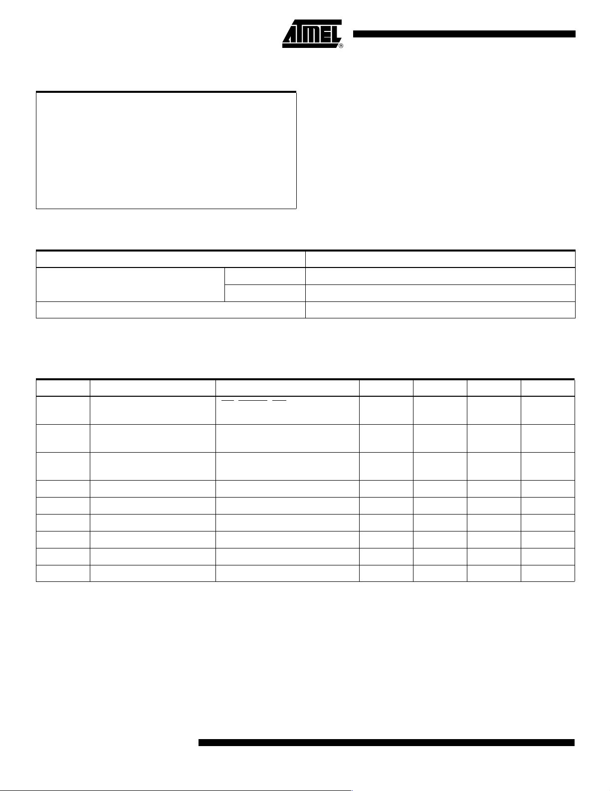
Absolute Maximum Ratings*
Temperature under Bias................................-55°C to +125°C
Storage Temperature.....................................-65°C to +150°C
All Input Voltages
(including NC Pins)
with Respect to Ground...................................-0.6V to +6.25V
All Output Voltages
with Respect to Ground.............................-0.6V to V
+ 0.6V
CC
*NOTICE: Stresses beyond those listed under “Absolute
Maximum Ratings” may cause permanent damage to the dev ice . This i s a stress r at ing onl y and
functional operati on of the de vic e at these or an y
other conditions beyond those indicated in the
operational sections of this specification is not
implied. Exposure to absolute maximum rating
conditions f or extend ed periods ma y affect d evice
reliability.
DC and AC Operating Range
AT45DB321B
Com. 0°C to 70°C
Operating Temperature (Case)
Ind. -40°C to 85°C
V
Power Supply
CC
(1)
2.7V to 3.6V
Note: 1. After power is applied and VCC is at the minimum specified datasheet value, the system should wait 20 ms before an opera-
tional mode is started.
DC Characteristics
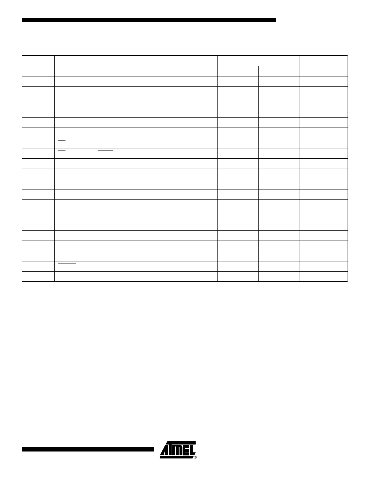
Symbol Parameter Condition Min Typ Max Units
I
SB
Standby Current CS, RESET, WP = VCC, all inputs
210µA
at CMOS levels
(1)
I
I
CC1
CC2
Active Current, Read
Operation
Active Current,
f = 20 MHz; I
V
= 3.6V
CC
= 0 mA;
OUT
410mA
VCC = 3.6V 15 35 mA
Program/Erase Operation
I
LI
I
LO
V
IL
V
IH
V
OL
V
OH
Note: 1. I
Input Load Current VIN = CMOS levels 1 µA
Output Leakage Current V
= CMOS levels 1 µA
I/O
Input Low Voltage 0.6 V
Input High Voltage 2.0 V
Output Low Voltage IOL = 1.6 mA; VCC = 2.7V 0.4 V
Output High Voltage IOH = -100 µA VCC - 0.2V V
during a buffer re ad is 20mA maximum.
cc1
12
AT45DB321B
2223D–DFLASH–10/02
Page 13
AC Characteristics
Symbol Parameter
AT45DB321B
AT45DB321B
UnitsMin Max
f
SCK
f
CAR
t
WH
t
WL
t
CS
t
CSS
t
CSH
t
CSB
t
SU
t
H
t
HO
t
DIS
t
V
t
XFR
t
EP
t
P
t
PE
t
BE
t
RST
t
REC
SCK Frequency 20 MHz
SCK Frequency for Continuous Array Read 20 MHz
SCK High Time 22 ns
SCK Low Time 22 ns
Minimum CS High Time 250 ns
CS Setup Time 250 ns
CS Hold Time 250 ns
CS High to RDY/BUSY Low 200 ns
Data In Setup Time 5 ns
Data In Hold Time 10 ns
Output Hold Time 0 ns
Output Disable Tim e 18 ns
Output Valid 20 ns
Page to Buffer Transfer/Compare Time 250 µs
Page Erase and Programming Time 20 ms
Page Programming Time 14 ms
Page Erase Time 8ms
Block Erase Time 12 ms
RESET Pulse Width 10 µs
RESET Recovery Time 1 µs
2223D–DFLASH–10/02
13
Page 14

Input Test Wavef orms and Measurement Levels
AC
DRIVING
LEVELS
tR, tF < 3 ns (10% to 90%)
2.4V
0.45V
2.0
0.8
Output T est Load
DEVICE
UNDER
TEST
30 pF
AC
MEASUREMENT
LEVEL
AC Waveforms
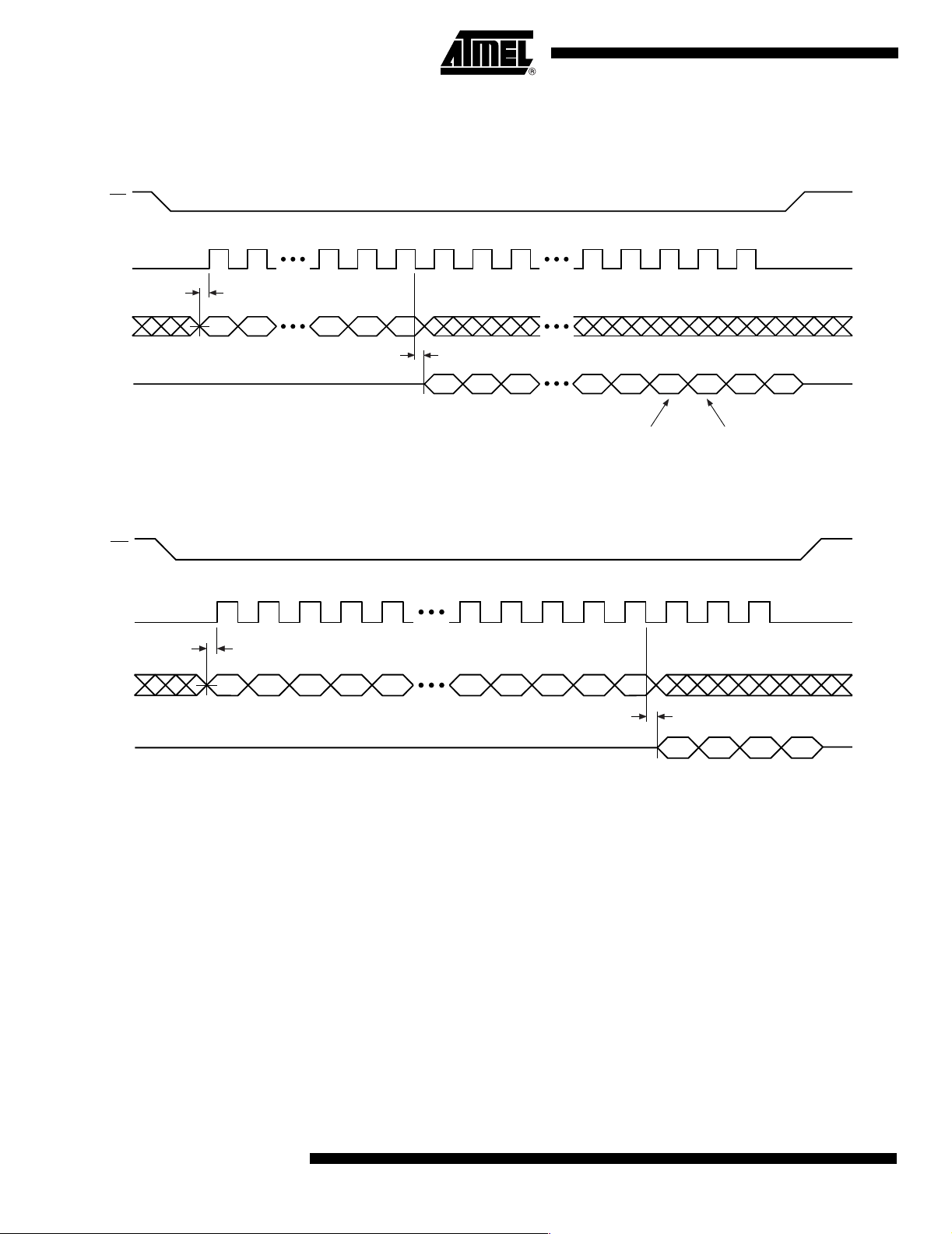
Two different timing diagrams are shown below. Waveform 1 shows the SCK signal
being low when CS
nal being high when CS
makes a high-to-low transition, and Waveform 2 shows the SCK sig-
makes a high-to-low transition. Both waveforms show valid
timing diagrams. The setup and hold times for the SI signal are referenced to the low-tohigh transition on the SCK signal.
Waveform 1 shows timing that is also compatible with SPI Mode 0, and Waveform 2
shows timing that is compatible with SPI Mode 3.
Waveform 1 – Inactive Clock Polarity Low and SPI Mode 0
CS
t
CSS
t
WH
t
WL
SCK
t
HO
VALID OUT
HIGH IMPEDANCE
SO
SI
t
V
t
SU
t
H
VALID IN
Waveform 2 – Inactive Clock Polarity High and SPI Mode 3
CS
t
CSH
t
CS
t
DIS
HIGH IMPEDANCE
t
CS
14
t
CSS
SCK
HIGH Z
SO
SI
AT45DB321B
t
WL
t
V
t
SU
t
WH
t
HO
VALID OUT
t
H
t
CSH
t
DIS
HIGH IMPEDANCE
VALID IN
2223D–DFLASH–10/02
Page 15

Reset Timing (Inactive Clock Polarity Low Shown)
CS
SCK
RESET
t
RST
t
REC
AT45DB321B
t
CSS
SO
HIGH IMPEDANCE HIGH IMPEDANCE
SI
Note: The CS signal should be in the high state before the RESET signal is deasserted.
Command Sequence for Read/Write Operations (except Status Register Read)
SI CMD 8 bits
MSB
Reserved for
larger densities
Page Address
(PA12-PA0)
Notes: 1. “r” designates bits reserved for larger densities.
2. It is recommended that “r” be a logical “0” for densities of 32M bits or smaller.
3. For densities larger than 32M bits, the “r” bits become the most significant Page Address bit for the appropriate density.
8 bits
(BA9-BA0/BFA9-BFA0)
8 bits
Byte/Buffer Address
LSBr X X X X X X X X X X X X X X X X X X X X X X X
2223D–DFLASH–10/02
15
Page 16

Write Operations The following block diagram and waveforms illustrate the various write sequences
available.
FLASH MEMORY ARRAY
PAGE (528 BYTES)
BUFFER 1 TO
MAIN MEMORY
PAGE PROGRAM
BUFFER 1
WRITE
THROUGH BUFFER 2
MAIN MEMORY PAGE
PROGRAM THROUGH
BUFFER 1
I/O INTERFACE
Main Memory Page Program through Buffers
CS
SI
CMD n n+1 Last Byte
r , PA12-6
PA5-0, BFA9-8
BFA7-0
Buffer Write
CS
MAIN MEMORY
PAGE PROGRAM
SI
BUFFER 2 TO
MAIN MEMORY
PAGE PROGRAM
BUFFER 2 (528 BYTES)BUFFER 1 (528 BYTES)
BUFFER 2
WRITE
· Completes writing into selected buffer
· Starts self-timed erase/program operation
· Completes writing into selected buffer
SI
CMD X
X···X, BFA9-8
BFA7-0
n
n+1
Last Byte
Buffer to Main Memory Page Program (Data from Buffer Programmed into Flash Page)
Starts self-timed erase/program operation
CS
Each transition represents
8 bits and 8 clock cycles
16
AT45DB321B
SI
CMD PA5-0, XX X
r , PA12-6
n = 1st byte read
n+1 = 2nd byte read
2223D–DFLASH–10/02
Page 17

AT45DB321B
Read Operations The following block diagram and waveforms illustrate the various r ead sequences
available.
FLASH MEMORY ARRAY
PAGE (528 BYTES)
MAIN MEMORY
PAGE TO
BUFFER 1
MAIN MEMORY
PAGE TO
BUFFER 2
BUFFER 2 (528 BYTES)BUFFER 1 (528 BYTES)
BUFFER 1
READ
MAIN MEMORY PAGE READ
BUFFER 2
READ
I/O INTERFACE
SO
Main Memory Page Read
CS
XXX
SO
SI
CMD
r , PA12-6
PA5-0, BA9-8
BA7-0 X
Main Memory Page to Buffer Transfer (Data from Flash Page Read into Buffer)
Starts reading page data into buffer
CS
n n+1
Buffer Read
ach transition represents
8 bits and 8 clock cycles
2223D–DFLASH–10/02
CS
SO
SI
SO
SI
CMD
CMD
X
r , PA12-6
X···X, BFA9-8
PA5-0, XX X
BFA7-0
X
n n+1
n = 1st byte read
n+1 = 2nd byte read
17
Page 18

Detailed Bit-level Read Timing – Inactive Clock Polarity Low
Continuous Array Read (Opcode: 68H)
CS
SCK
SI
SO
t
SU
12 63 64 65 66 67 68
1XX
0
t
V
HIGH-IMPEDANCE
Main Memory Page Read (Opcode: 52H)
CS
SCK
SI
t
SU
12345 60 61 62 63 64 65 66 67
COMMAND OPCODE
0
10
1
0
DATA OUT
D7D6D
XXX
LSB MSB
D
5
D1D0D7D6D
2
BIT 4223
OF
PAGE n
XX
PAGE n+1
BIT 0
OF
5
SO
HIGH-IMPEDANCE
t
V
DATA OUT
D
7
MSB
D
D
6
5
18
AT45DB321B
2223D–DFLASH–10/02
Page 19

AT45DB321B
Detailed Bit-level Read Timing – Inactive Clock Polarity Low (Continued)
Buffer Read (Opcode: 54H or 56H)
CS
SCK
SI
SO
t
SU
12345 36 37 38 39 40 41 42 43
COMMAND OPCODE
0
10
1
0
HIGH-IMPEDANCE
Status Register Read (Opcode: 57H)
CS
SCK
SO
SI
t
SU
12345 7891011 12 16 17
COMMAND OPCODE
0
10
1
0
HIGH-IMPEDANCE
XXX
6
111
t
XX
t
V
V
STATUS REGISTER OUTPUT
D
D
7
MSB
D
6
5
DATA OUT
D
7
MSB
D
1
D
6
D
LSB MSB
D
5
D
0
7
2223D–DFLASH–10/02
19
Page 20

Detailed Bit-level Read Timing – Inactive Clock Polarity High
Continuous Array Read (Opcode: 68H)
CS
SCK
SI
SO
12 63 64 65 66 67
t
SU
1XXX
0
t
V
HIGH-IMPEDANCE
Main Memory Page Read (Opcode: 52H)
CS
SCK
SI
12345 61 62 63 64 65 66 67
t
SU
COMMAND OPCODE
1
0
0
10
DATA OUT
D7D6D
XXX
LSB MSB
5
D2D
XX
D0D7D6D
1
BIT 4223
OF
PAGE n
PAGE n+1
BIT 0
OF
5
68
SO
HIGH-IMPEDANCE
t
V
D
MSB
7
DATA OUT
D
D
6
5
D
4
20
AT45DB321B
2223D–DFLASH–10/02
Page 21

AT45DB321B
Detailed Bit-level Read Timing – Inactive Clock Polarity High (Continued)
Buffer Read (Opcode: 54H or 56H)
CS
SCK
SI
SO
12345 37 38 39 40 41 42 43
t
SU
COMMAND OPCODE
1
0
0
10
HIGH-IMPEDANCE
Status Register Read (Opcode: 57H)
CS
SCK
SI
SO
12345 7891011 12 17 18
t
SU
0
COMMAND OPCODE
0
10
1
HIGH-IMPEDANCE
XXX
6
111
t
V
D
MSB
XX
t
V
D
MSB
STATUS REGISTER OUTPUT
D
D
7
6
D
5
4
DATA OUT
D
7
D
6
D
0
LSB MSB
44
D
5
4
D
D
7
6
2223D–DFLASH–10/02
21
Page 22
Detailed Bit-level Read Timing – SPI Mode 0
Continuous Array Read (Opcode: E8H)
CS
SCK
SI
SO
t
SU
12 62 63 64 65 66 67
1XXX
1
t
V
HIGH-IMPEDANCE
Main Memory Page Read (Opcode: D2H)
CS
SCK
SI
t
SU
12345 60 61 62 63 64 65 66 67
COMMAND OPCODE
0
10
1
1
DATA OUT
D7D6D
XXX
LSB MSB
5
D2D
XX
D0D7D6D
1
BIT 4223
OF
PAGE n
PAGE n+1
BIT 0
OF
5
22
SO
AT45DB321B
HIGH-IMPEDANCE
t
V
D
MSB
7
DATA OUT
D
D
6
5
D
4
2223D–DFLASH–10/02
Page 23

Detailed Bit-level Read Timing – SPI Mode 0 (Continued)
Buffer Read (Opcode: D4H or D6H)
CS
AT45DB321B
SCK
t
SU
12345 36 37 38 39 40 41 42 43
COMMAND OPCODE
SI
SO
1
1
10
0
HIGH-IMPEDANCE
Status Register Read (Opcode: D7H)
CS
SCK
SI
SO
t
SU
12345 7891011 12 16 17
COMMAND OPCODE
0
10
1
1
HIGH-IMPEDANCE
XXX
6
111
t
V
D
MSB
7
XX
t
V
D
MSB
7
DATA OUT
D
6
STATUS REGISTER OUTPUT
D
6
D
D
4
5
D
D
5
1
D
4
D
D
0
LSB MSB
7
2223D–DFLASH–10/02
23
Page 24

Detailed Bit-level Read Timing – SPI Mode 3
Continuous Array Read (Opcode: E8H)
CS
SCK
SI
SO
12 63 64 65 66 67
t
SU
1XXX
1
t
V
HIGH-IMPEDANCE
Main Memory Page Read (Opcode: D2H)
CS
SCK
SI
12345 61 62 63 64 65 66 67
t
SU
COMMAND OPCODE
0
10
1
1
DATA OUT
D7D6D
XXX
LSB MSB
5
D2D
XX
D0D7D6D
1
BIT 4223
OF
PAGE n
PAGE n+1
BIT 0
OF
5
68
24
SO
AT45DB321B
HIGH-IMPEDANCE
t
V
D
MSB
7
DATA OUT
D
D
6
5
D
4
2223D–DFLASH–10/02
Page 25

Detailed Bit-level Read Timing – SPI Mode 3 (Continued)
Buffer Read (Opcode: D4H or D6H)
CS
AT45DB321B
SCK
12345 37 38 39 40 41 42 43
t
SU
COMMAND OPCODE
SI
SO
1
1
10
0
HIGH-IMPEDANCE
Status Register Read (Opcode: D7H)
CS
SCK
SI
SO
12345 7891011 12 17 18
t
SU
COMMAND OPCODE
0
10
1
1
HIGH-IMPEDANCE
XXX
6
111
t
V
D
MSB
XX
t
V
D
7
MSB
STATUS REGISTER OUTPUT
D
D
7
6
D
5
4
DATA OUT
D
D
6
5
D
0
LSB MSB
44
D
4
D
D
7
6
2223D–DFLASH–10/02
25
Page 26
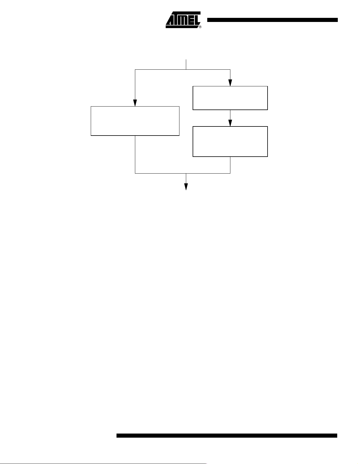
Figure 1. Algorithm for Sequentially Programming or Reprogramming the Entire Array
START
provide address
and data
BUFFER WRITE
(84H, 87H)
MAIN MEMORY PAGE PROGRAM
THROUGH BUFFER
(82H, 85H)
BUFFER TO MAIN
MEMORY PAGE PROGRAM
(83H, 86H)
END
Notes: 1. This type of algorithm is used for applications in which the entire array is programmed sequentially, filling the array page-by-
page.
2. A page can be written using either a Main Memory Page Program operation or a Buffer Write operation followed by a Buffer
to Main Memory Page Program operation.
3. The algorithm above shows the programming of a single page. The algorithm will be repeated sequentially for each page
within the entire array.
26
AT45DB321B
2223D–DFLASH–10/02
Page 27

Figure 2. Algorithm for Randomly Modifying Data
AT45DB321B
START
provide address of
page to modify
TO BUFFER TRANSFER
MAIN MEMORY PAGE PROGRAM
THROUGH BUFFER
(82H, 85H)
AUTO PAGE REWRITE
MAIN MEMORY PAGE
(53H, 55H)
(58H, 59H)
INCREMENT PAGE
ADDRESS POINTER
If planning to modify multiple
bytes currently stored within
a page of the Flash array
BUFFER WRITE
(84H, 87H)
BUFFER TO MAIN
MEMORY PAGE PROGRAM
(83H, 86H)
(2)
(2)
END
Notes: 1. To preserve data integrity, each page of a DataFlash sector must be updated/rewritten at least once within every 10,000
cumulative page erase/progr am operations.
2. A Page Address Pointer must be maintained to indicate which page is to be rewritten. The Auto Page Rewrite command
must use the address specified by the Page Address Pointer.
3. Other algorithms can be used to rewrite portions of the Flash array. Low-power applications may choose to wait until 10,000
cumulative page erase/program operations have accumulated before rewriting all pages of the sector. See application note
AN-4 (“Using Atmel’s Serial DataFlash”) for more details.
Sector Addressing
PA12 PA11 PA10 PA9 PA8 PA7 PA6 PA5 PA4 PA3 Sector
0 0 0 0000000 0
0000XXXXXX1
0001XXXXXX2
0010XXXXXX3
• • • ••••••• •
• • • ••••••• •
• • • ••••••• •
1100XXXXXX13
1101XXXXXX14
1110XXXXXX15
1111XXXXXX16
2223D–DFLASH–10/02
27
Page 28
Orderi ng Information
f
SCK
(MHz)
20 10 0.01 AT45DB321B-CC
20 10 0.01 AT45DB321B-CI
ICC (mA)
Ordering Code Package Operation RangeActive Standby
AT45DB321B-RC
AT45DB321B-TC
AT45DB321B-RI
AT45DB321B-TI
44C1
28R
32T
44C1
28R
32T
Commercial
(0°C to 70°C)
Industrial
(-40°C to 85°C)
Package Type
44C1 44-ball (5 x 9 Array), 1.0 mm Pitch, Plastic Chip-scale Ball Grid Array (CBGA)
28R 28-lead, 0.330" Wide, Plastic Gull Wing Small Outline Package (SOIC)
32T 32-lead, Plastic Thin Small Outline Package (TSOP)
28
AT45DB321B
2223D–DFLASH–10/02
Page 29
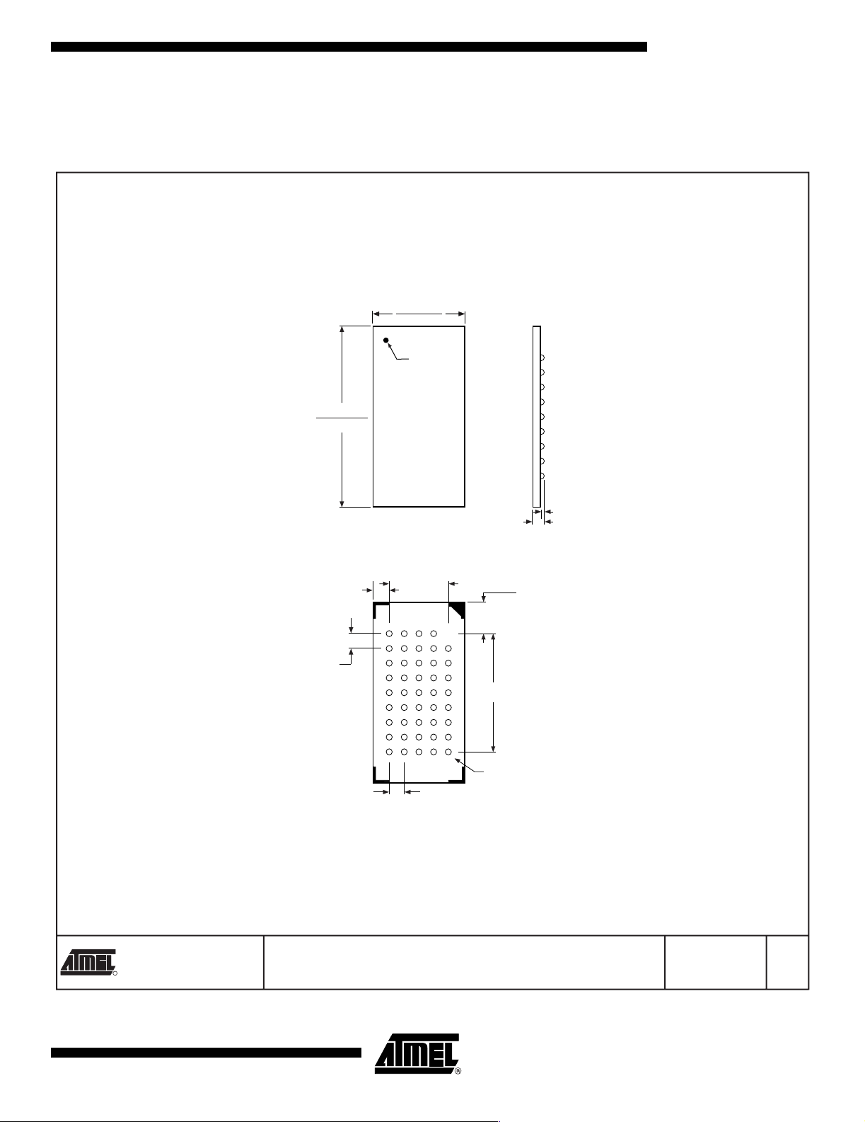
Packaging Information
44C1 – CBGA
Dimensions in Millimeters and (Inches).
Controlling dimension: Millimeters.
12.10(0.476)
11.90(0.468)
AT45DB321B
6.10(0.240)
5.90(0.232)
A1 ID
SIDE VIEW
NON-ACCUMULATIVE
2325 Orchard Parkway
R
San Jose, CA 95131
0.25 (0.010)MIN
1.20 (0.047) MAX
2.00 (0.079)REF
1.00 (0.039)REF
1.00 (0.0394) BSC
1.00 (0.0394) BSC
NON-ACCUMULATIVE
54 3 21
A
B
C
D
E
F
G
H
J
TOP VIEW
4.0 (0.157)
8.0 (0.315)
0.40 (0.016)
DIA BALL TYP
BOTTOM VIEW
TITLE
44C1, 44-ball (5 x 9 Array), 6 x 12 x 1.2 mm Body, 1.0 mm Ball
Pitch Chip-scale Ball Grid Array Package (CBGA)
DRAWING NO.
44C1
04/11/01
REV.
A
2223D–DFLASH–10/02
29
Page 30
32T – TSOP
PIN 1
Pin 1 Identifier
D1
D
e
E
b
A2
A
SEATING PLANE
A1
Notes: 1. This package conforms to JEDEC reference MO-142, Variation BD.
2. Dimensions D1 and E do not include mold protrusion. Allowable
protrusion on E is 0.15 mm per side and on D1 is 0.25 mm per side.
3. Lead coplanarity is 0.10 mm maximum.
0º ~ 8º
L
COMMON DIMENSIONS
SYMBOL
A – – 1.20
A1 0.05 – 0.15
A2 0.95 1.00 1.05
D 19.80 20.00 20.20
D1 18.30 18.40 18.50 Note 2
E 7.90 8.00 8.10 Note 2
L 0.50 0.60 0.70
L1 0.25 BASIC
b 0.17 0.22 0.27
c 0.10 – 0.21
e 0.50 BASIC
c
L1
GAGE PLANE
(Unit of Measure = mm)
MIN
NOM
MAX
NOTE
30
2325 Orchard Parkway
R
San Jose, CA 95131
AT45DB321B
TITLE
32T, 32-lead (8 x 20 mm Package) Plastic Thin Small Outline
Package, Type I (TSOP)
DRAWING NO.
32T
2223D–DFLASH–10/02
10/18/01
REV.
B
Page 31

28R – SOIC
AT45DB321B
B
E
1
PIN 1
e
D
A
1
0º ~ 8º
C
L
Note: 1. Dimensions D and E1 do not include mold Flash
or protrusion. Mold Flash or protrusion shall not exceed
0.25 mm (0.010").
E
A
COMMON DIMENSIONS
(Unit of Measure = mm)
SYMBOL
A 2.39 – 2.79
A1 0.002 – 0.014
D 18.00 – 18.50 Note 1
E 11.70 – 12.50
E1 8.59 – 8.79 Note 1
B 0.356 – 0.508
C 0.203 – 0.305
L 0.94 – 1.27
e 1.27 TYP
MIN
NOM
MAX
NOTE
2325 Orchard Parkway
R
San Jose, CA 95131
2223D–DFLASH–10/02
TITLE
28R, 28-lead, 0.330" Body Width,
Plastic Gull Wing Small Outline (SOIC)
10/08/2002
DRAWING NO.
28R
REV.
B
31
Page 32

Atmel Headquarters Atmel Operations
Corporate Headquarters
2325 Orchard Parkway
San Jose, CA 95131
TEL 1(408) 441-0311
FAX 1(408) 487-2600
Europe
Atmel Sarl
Route des Arsenaux 41
Case Postale 80
CH-1705 Fribourg
Switzerland
TEL (41) 26-426-5555
FAX (41) 26-426-5500
Asia
Room 1219
Chinachem Gol den P laza
77 Mody Road Tsimshatsui
East Kowloon
Hong Kong
TEL (852) 2721-9778
FAX (852) 2722-1369
Japan
9F, Tonetsu Shinkawa Bldg.
1-24-8 Shin kawa
Chuo-ku, Tokyo 104-0033
Japan
TEL (81) 3- 3523-3 551
FAX (81) 3-3523-7581
Memory
2325 Orchard Parkway
San Jose, CA 95131
TEL 1(408) 441-0311
FAX 1(408) 436-4314
Microcontrollers
2325 Orchard Parkway
San Jose, CA 95131
TEL 1(408) 441-0311
FAX 1(408) 436-4314
La Chantrerie
BP 70602
44306 Nantes Cedex 3, France
TEL (33) 2-40-18-18-18
FAX (33) 2- 40-18- 19-6 0
ASIC/ASSP/Smart Cards
Zone Industrielle
13106 Rousset Cedex, France
TEL (33) 4-42-53-60-00
FAX (33) 4- 42-53- 60-0 1
1150 East Cheyenne Mtn. Blvd.
Colorado Springs, CO 80906
TEL 1(719) 576-3300
FAX 1(719) 540-1759
Scottish Enterprise Technology Park
Maxwell Building
East Kilbride G75 0QR, Scotland
TEL (44) 1355-803-000
FAX (44) 1355-242-743
RF/Automotive
Theresienstrasse 2
Postfach 3535
74025 Heilbro nn, Ge rmany
TEL (49) 71-31-67-0
FAX (49) 71-31-67-2340
1150 East Cheyenne Mtn. Blvd.
Colorado Springs, CO 80906
TEL 1(719) 576-3300
FAX 1(719) 540-1759
Biometrics/Imaging/Hi-Rel MPU/
High Speed Converters/RF Datacom
Avenue de Rochepleine
BP 123
38521 Saint-Egreve Cedex, France
TEL (33) 4-76-58-30-00
FAX (33) 4- 76-58- 34-8 0
e-mail
literature@atmel.com
Web Site
http://www.atmel.com
© Atmel Corporation 2002.
Atmel Corporation makes no warranty for the use of its products, other than those expressly contained in the Company’s standard warranty
which is detailed in Atmel’s Terms and Conditions loc ated on the Company’s web site. The Company assumes no responsibility for any errors
which may appear in this document, reserves the right to change devices or specifications detailed herein at any time without notice, and does
not make any commitment to update the information contained herein. No licenses to patents or other intellectual property of Atmel are granted
by the Company in connection with the sale of Atmel products, expressly or by implication. Atmel’s products are not authorized for use as critical
components in life support devices or systems.
Atmel® and DataFlash® are the registered trademarks of Atmel.
Other terms and product names may be the trademarks of others
Printed on recycled paper.
2223D–DFLASH–10/02
/xM
 Loading...