

Page 1
Features
• Configurations:
– Can be configured as a combination of touchscreen, sliders/wheels and keys, with
Adjacent Key Suppression
• QField
™
Touchscreen:
– Two-touch capable with independent XY tracking for one or two concurrent
touches in real time, with touch size reporting
– Up to eight-inch diagonal screen size supported
– 1024 x 1024 resolution
• Discrete Keys:
– Up to 48 (subject to other configurations)
• QSlide
™
/QWheel™:
– Configurable up to six independent sliders/wheels
• Linearity:
– Screen design dependent but typically better than ±1 percent
• Filtering:
– Advanced digital filtering (user configurable)
• Response Times:
– Sub 15 ms possible, depending on filter settings
• General Purpose Outputs (GPOs):
– Up to four user controllable outputs
• Technolo g y:
– Patented charge-transfer (transverse mode)
• Panel Thickness:
– Glass up to 5 mm, screen size dependent
– Plastic up to 3 mm, screen size dependent
• Channel Sensitivity:
– Individually settable via simple commands over serial interface
• Interface:
2
C-compatible slave mode, 100 kHz or 400 kHz with 2.7V or greater Vdd
–I
• Power:
– 1.8V to 5.5V (2.7V to 5.5V in high speed mode)
• Packages:
– 44-pin 7 x 7 mm MLF RoHS compliant
– 44-pin 10 x 10 mm TQFP RoHS compliant
– 49-ball 5 x 5 mm BGA RoHS compliant
• Signal Processing:
– Self-calibration, auto drift compensation, noise filtering, Adjacent Key
Suppression technology
™
(AKS™) technology between groups
QTwo™ 10-bit
Touchscreen
Controller
AT42QT5480
Summary
Note: This is a summary document. A
complete document is available under
NDA. For more information contact
www.atmel.com/touchscreen.
9510AS–AT42–10/08
Page 2
1. Pinout and Schematic
GPO1
CHANGE
VREF
SMP
GPO0
Vss
Vdd
Y0B
Y1B
Y2B
Y3B
X3X4X5X6X7
Vdd
Vss
SCL
SDA
Y0A
Y1A
GPO2
GPO3
TRIGGER
RST
Vdd
Vss
XT2
XT1
X0
X1
X2
Y2A
Y3A
Y4A
Y5A
Vdd
Vss
Vdd
A0
FORCE_S
Y5B
Y4B
1
2
3
4
5
6
7
8
9
10
11 23
24
25
26
27
28
29
30
31
32
33
44
43
42
41
403938
37
36
34
35
12
13
14 22
21
19
2018
17
1615
QT5480
QT5480
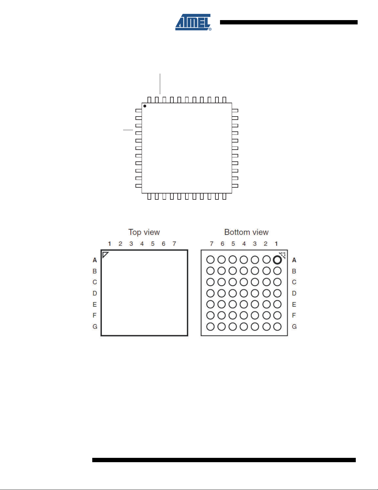
1.1 Pinout Configurations
2
QT5480
9510AS–AT42–10/08
Page 3

QT5480
1.2 Pin Descriptions
Table 1-2. Pin Listing
Pin Ball Name Type Comments If Unused, Connect To...
1 B2 GPO2 O General purpose output 2 Leave open
2 B1 GPO3 O General purpose output 3 Leave open
3 C3 TRIGGER I Trigger input (active low) Vss
4C2 RST
5A5 Vdd PPower –
6 A1 Vss P Supply ground –
7 D2 XT2 X Clock resonator –
8 E1 XT1 X Clock resonator –
9 D3 X0 O X matrix drive line Leave open
10 E2 X1 O X matrix drive line Leave open
11 F1 X2 O X matrix drive line Leave open
12 F2 X3 O X matrix drive line Leave open
13 G2 X4 O X matrix drive line Leave open
I Reset low; has internal 30k - 60k pull-up Leave open or Vdd
14 E3 X5 O X matrix drive line Leave open
15 F3 X6 O X matrix drive line Leave open
16 E4 X7 O X matrix drive line Leave open
17 C1 Vdd P Power –
18 A4 Vss P Supply ground –
19 F4 SCL OD Serial Interface Clock –
20 G5 SDA OD Serial Interface Data –
21 F5 Y0A I Y line connection Leave open
22 G6 Y1A I Y line connection Leave open
23 F6 Y2A I Y line connection Leave open
24 E5 Y3A I Y line connection Leave open
25 F7 Y4A I Y line connection Leave open
26 E6 Y5A I Y line connection Leave open
27 E7 Vdd P Power –
28 A7 Vss P Supply ground –
29 C7 Vdd P Power –
30 D6 A0 I I2C-compatible address select –
31 C6 FORCE_S I Force sensor input Vdd or Vss
32 B7 Y5B I Y line connection Leave open
33 D5 Y4B I Y line connection Leave open
34 B6 Y3B I Y line connection Leave open
35 A6 Y2B I Y line connection Leave open
9510AS–AT42–10/08
3
Page 4

Table 1-2. Pin Listing (Continued)
Pin Ball Name Type Comments If Unused, Connect To...
36 C5 Y1B I Y line connection Leave open
37 B5 Y0B I Y line connection Leave open
38 G3 Vdd P Power –
39 D1 Vss P Supply ground –
40 B4 GPO0 O General purpose output 0 Leave open
41 C4 SMP O Sample output. –
42 A3 Vref I Reference input –
43 B3 CHANGE
44 A2 GPO1 O General purpose output 1 Leave open
– D4 Vss P Supply ground –
– D7 Vss P Supply ground –
– G1 Vss P Supply ground –
– G4 Vss P Supply ground –
– G7 Vss P Supply ground –
OD State change notification –
4
QT5480
9510AS–AT42–10/08
Page 5

1.3 Schematic
Rs3
Rp
Rx4
Rx5
VREG
Rs5 Rs4
Cs5
Cs4
Cs2
Cs1
Rx3
Rs2 Rs1 Rs0
Ry4
Ry1
Rp
Rp
XT1
16MHz
Cs3
Cs0
Rx7
Rx1
Ry5
Ry2
Vunreg
VDD
Ry3
Ry0
MATRIX X DRIVE
MATRIXYSCANIN
Rx0
Rx6
VDD
Follow regulator manufacturer's recommended values
for input and output bypass capacitors (Creg).
Rx2
Add two 100nF capacitors: one close to pins 5, 17 and 38,
and another close to pins 27 and 29.
QT5480
NOTES:
1) The central pad on the underside of the MLF chip
is a Vss pin and should be connected to ground.
Do not put any other tracks underneath
the body of the chip.
2) It is important to place all Cs, Rs, Rx and Ry
components physically near to the chip.
3) Leave YnA, YnB unconnected if not used
Figure 1-1. Typical Circuit
QT5480
9510AS–AT42–10/08
5
Page 6
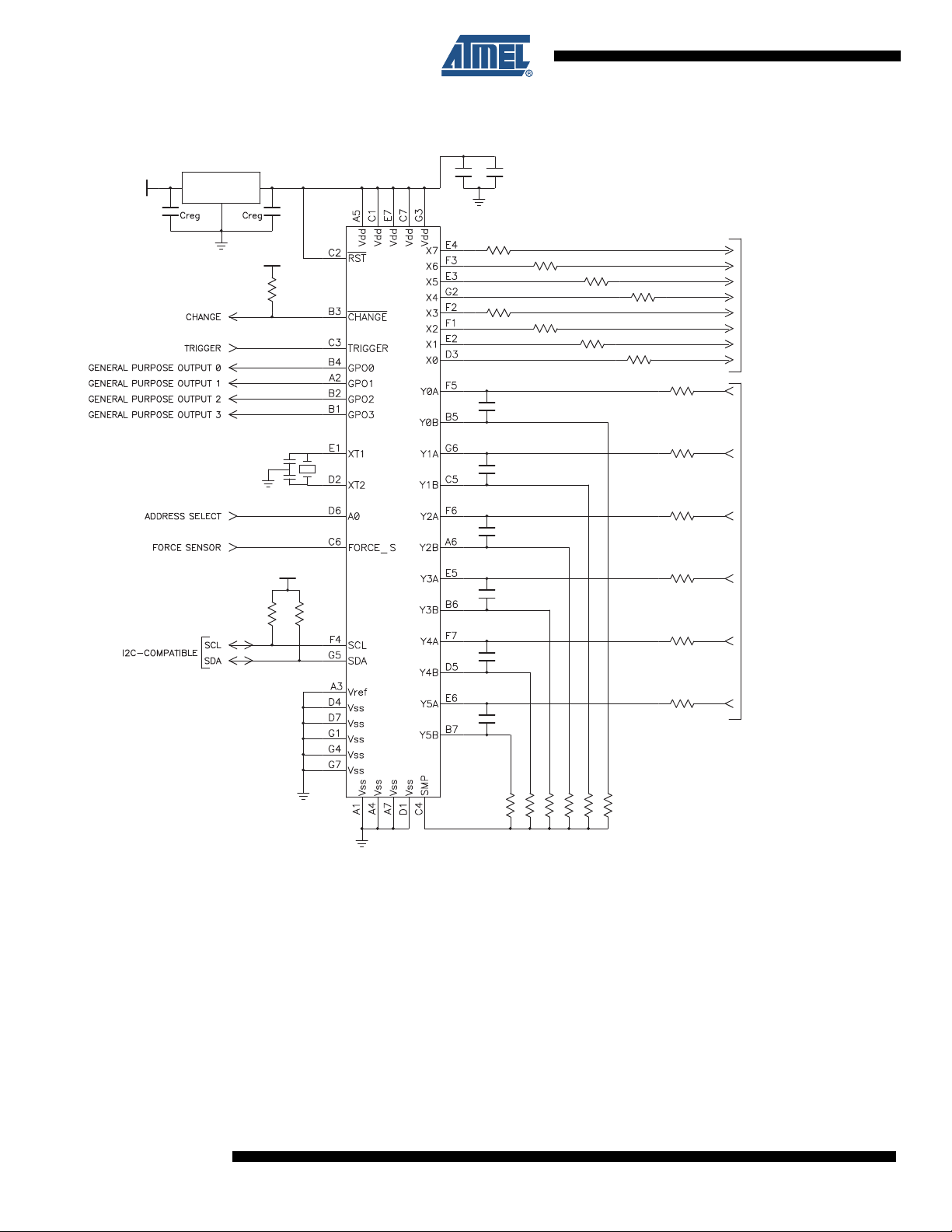
Figure 1-2. Typical Circuit – BGA
Cs4
Cs1
Rs4
Cs5
Cs3
Cs2
Cs0
VDD
Vunreg
Rp
VREG
Rp
16MHz
Rs5
Rx3
Rs2 Rs1 Rs0
Ry3
Ry0
Rp
VDD
XT1
Rx7
Rx5
Rx1
Ry5
Ry2
MATRIX X DRIVE
Ry4
Ry1
MATRIXYSCANIN
Rs3
Rx0
Rx6
Rx2
Rx4
QT5480
Follow regulator manufacturer's recommended values
for input and output bypass capacitors (Creg).
NOTES:
1) It is important to place all Cs, Rs, Rx and Ry
components physically near to the chip.
2) Leave YnA, YnB unconnected if not used
Add two 100nF capacitors: one close to balls A5, C1 and G3,
and another close to balls E7 and C7.
Suggested regulator manufacturers:
• Torex (XC6215 series)
• Seiko (S817 series)
• BCDSemi (AP2121 series)
6
QT5480
9510AS–AT42–10/08
Page 7

2. Overview of the QT5480
2.1 Introduction
The QT5480 is a versatile capacitive touchscreen controller, able to support a diagonal
touchscreen of up to 8 inches. The IC supports Two Touch
of devices from Atmel
The QT5480 uses Atmel's patented QMatrix
excellent moisture tolerance, fast acquisition and outstanding ground load immunity.
A unique feature of the QT5480 is that it allows a choice to be made as to how many of the
capacitive measurement channels form part of a touchscreen, and which ones form discrete
keys or sliders.
This controller offers unrivalled flexibility to create touchscreens, sliders and keys. The device can
report two touches on a touchscreen making it suitable for next generation touch interfaces.
Concurrent use of a touchscreen plus keys or sliders is also possible.
By treating all capacitive channels equally during measurement, and then applying additional signal
processing, the device allows the channels to be used as part of a touchscreen, or part of one or more
sliders, or as discrete touch keys.
QT5480
™
®
.
™
capacitive sensing technique, which offers
operation, part of the QTwo™ family
Touchscreens can be created that are of arbitrary channel length and width. Channels not used in the
touchscreen can either be turned into sliders or keys. There are some constraints on the starting
channels for touchscreens and sliders, but these have no practical impact for most applications.
The controller also has the ability to save a Y line when configuring a touchscreen, reusing it in the
touchscreen pattern at the two edges. This saved Y line can then be used to create extra objects like
a slider or multiple keys, while allowing the touchscreen to be sized as though it was “one Y line
larger”. In this “wrapped Y line” mode Two Touch processing cannot be used.
See Figure 2-1 for configuration examples.
9510AS–AT42–10/08
7
Page 8

Figure 2-1. Example Touchscreen Configurations
Y3
Y2
Y1
Y0
X0 X1 X2 X3 X4 X5 X6 X7
QT5480
Y4
Y5
Y3
Y2
Y1
Y0
X0 X1 X2 X3 X4 X5 X6 X7
QT5480
Y4
Y5
Y
X
Y
X
= slider
= touchscreen
= key
= disabled
Object Color Code
8
QT5480
9510AS–AT42–10/08
Page 9

3. Revision History
Revision No. History
Revision AS – October 2008 Initial release for chip revision 5.0
QT5480
9510AS–AT42–10/08
9
Page 10

Headquarters International
Atmel Corporation
2325 Orchard Parkway
San Jose, CA 95131
USA
Tel: 1(408) 441-0311
Fax: 1(408) 487-2600
Atmel Asia
Unit 01-05 & 16, 19/F
BEA Tower, Millennium City 5
418 Kwun Tong Road
Kwun Tong
Kowloon
Hong Kong
Tel: (852) 2245-6100
Fax: (852) 2722-1369
Touch Technology Division
1 Mitchell Point
Ensign Way
Hamble
Southampton
Hampshire SO31 4RF
United Kingdom
Tel: (44) 23-8056-5600
Fax: (44) 23-8045-3939
Product Contact
Web Site
www.atmel.com
Atmel Europe
Le Krebs
8, Rue Jean-Pierre Timbaud
BP 309
78054 Saint-Quentin-enYvelines Cedex
France
Tel: (33) 1-30-60-70-00
Fax: (33) 1-30-60-71-11
Technical Support
touch@atmel.com
Atmel Japan
9F, Tonetsu Shinkawa Bldg.
1-24-8 Shinkawa
Chuo-ku, Tokyo 104-0033
Japan
Tel: (81) 3-3523-3551
Fax: (81) 3-3523-7581
Sales Contact
www.atmel.com/contacts
Literature Requests
www.atmel.com/literature
Disclaimer: The information in this document is provided in connection with Atmel products. No license, express or implied, by estoppel or otherwise, to any
intellectual property right is granted by this document or in connection with the sale of Atmel products. EXCEPT AS SET FORTH IN ATMEL’S TERMS AND
CONDITIONS OF SALE LOCATED ON ATMEL’S WEB SITE, ATMEL ASSUMES NO LIABILITY WHATSOEVER AND DISCLAIMS ANY EXPRESS, IMPLIED OR
STATUTORY WARRANTY RELATING TO ITS PRODUCTS INCLUDING, BUT NOT LIMITED TO, THE IMPLIED WARRANTY OF MERCHANTABILITY, FITNESS FOR
A PARTICULAR PURPOSE, OR NON-INFRINGEMENT. IN NO EVENT SHALL ATMEL BE LIABLE FOR ANY DIRECT, INDIRECT, CONSEQUENTIAL, PUNITIVE,
SPECIAL OR INCIDENTAL DAMAGES (INCLUDING, WITHOUT LIMITATION, DAMAGES FOR LOSS OF PROFITS, BUSINESS INTERRUPTION, OR LOSS OF
INFORMATION) ARISING OUT OF THE USE OR INABILITY TO USE THIS DOCUMENT, EVEN IF ATMEL HAS BEEN ADVISED OF THE POSSIBILITY OF SUCH
DAMAGES. Atmel makes no representations or warranties with respect to the accuracy or completeness of the contents of this document and reserves the right to
make changes to specifications and product descriptions at any time without notice. Atmel does not make any commitment to update the information contained
herein. Unless specifically provided otherwise, Atmel products are not suitable for, and shall not be used in, automotive applications. Atmel’s products are not
intended, authorized, or warranted for use as components in applications intended to support or sustain life.
© 2008 Atmel Corporation. All rights reserved. Atmel®, Atmel logo and combinations thereof, and others are registered trademarks, Adjacent
Key Suppression
™
, AKS™, QField™, QMatrix™, QTouch™, QSlide™, QWheel™, Tw o To u c h™, QTwo™ and others are trademarks of Atmel
Corporation or its subsidiaries. Other terms and product names may be registered trademarks or trademarks of others.
9510AS–AT42–10/08
 Loading...