

Page 1
Features
Y2A
Y1A
Y0A
RST
SCL
SDA
N/C
Y2B
Vss
VREF
SMPX0X1X2X3
N/C
N/C
CHANGE
Vss
Vdd
Vss
Vdd
N/C
N/C
N/C
Vdd
Vdd
Vss
A0
Y0B
Y1B
1
2
3
4
5
6
7
817
18
19
20
21
22
23
24
32
31
30
29
282726
25
9
10
11
16
15
14
13
12
AT42QT4120
Vdd
• QField
• Techn ology:
• Panel Materials:
• Adjacent Metal:
• Panel Thickness:
• Interface:
• Moisture Tolerance:
• Power:
• Packages:
• Signal Processing:
• Applications:
• Patents:
™
Touchscreen:
– Up to 3.4 inches diagonal screen size supported
– Patented spread-spectrum charge-transfer (transverse mode)
– Plastic, glass, composites, painted surfaces (low particle density metallic paints
possible)
– Compatible with grounded metal immediately next to sensing channels
– 1 to 2 mm glass, 0.5 to 1.5 mm plastic
–I2C-compatible slave mode, 100 kHz or 400 kHz
– Best in class
– 1.8V to 5.5V (2.5V to 5.5V in high speed mode)
– 32-pin 5 x 5 mm MLF RoHS compliant
– Self-calibration, auto drift compensation, noise filtering
– Mobile electronics, terminals, appliances
– QMatrix™ (patented Charge-transfer method)
– QField (patented Charge-transfer method, patent-pending QField optimized for
one-layer sensor element designs)
QField™ 10-bit
Touchscreen
Sensor IC
AT42QT4120
Summary
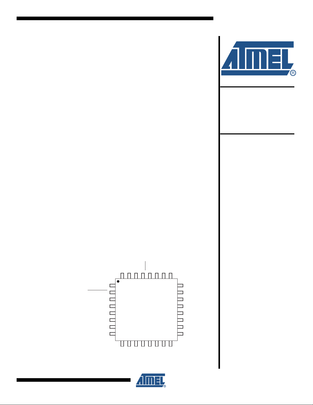
1. Pin-out and Pin Listing Descriptions
1.1 Device Pin-out
Note: This is a summary document. A
complete document is available under
NDA. For more information contact
www.atmel.com/touchscreen.
9506AS–AT42–10/08
Page 2

1.2 Pin Listing Description
Table 1-1. Pin Listing
Pin Name Type Comments If Unused, connect To...
1 N/C O Not connected Leave open
2 CHANGE OD State change notification Leave open
3 Vss P Supply ground –
4 Vdd P Power –
5 Vss P Supply ground –
6 Vdd P Power –
7 N/C O Not connected Leave open
8 N/C O Not connected Leave open
9 Vss P Supply ground –
10 VREF I Supply ground –
11 SMP O Sample output –
12 X0 O X matrix drive line Leave open
13 X1 O X matrix drive line Leave open
14 X2 O X matrix drive line Leave open
15 X3 O X matrix drive line Leave open
16 N/C O Not connected Leave open
17 N/C O Not connected Leave open
18 Vdd P Power –
19 Vdd P Power –
20 Vdd P Power –
21 Vss P Supply ground –
22 A0 I I2C-compatible address select –
23 Y0B I/O Y line connection Leave open
24 Y1B I/O Y line connection Leave open
25 Y2B I/O Y line connection Leave open
26 N/C O Not connected Leave open
27 SDA OD Serial Interface Data –
28 SCL OD Serial Interface Clock –
29 RST I Reset low; has internal 30k - 60k pull-up Leave open or Vdd
30 Y0A O Y line connection Leave open
31 Y1A O Y line connection Leave open
32 Y2A O Y line connection Leave open
I Input only I/O Input and output
O Output only, push-pull X Clock resonator
OD Open drain output P Ground or power
2
AT42QT4120
9506AS–AT42–10/08
Page 3

1.3 Wiring Diagram
Rp Rp
Rs2 Rs0
Ry2
Ry1
Ry0
SCL
SDA
VREG
Rx2
Rc
VDD
Rs1
Rx3
Cs2
Cs1
Cs0
Rx0
Vunreg
VDD
Rx1
N/C
N/C
CHANGE
QT4120
N/C
N/C
N/C
N/C
VDD
MATRIXYSCANIN
follow regulator manufacturer's recommended values for input
and output bypass capacitors; keep output capacitor close to
pins 4 and 6. If not possible, add a 100nF capacitor next to those pins.
MATRIX X DRIVE
NOTES:
1) The central pad on the underside of the chip
is a Vss pin and should be connected to ground.
Do not put any other tracks underneath
the body of the chip.
2) It is important to place all Cs, Rs, Rx and Ry
components physically near to the chip.
I C-COMPATIBLE
2
I C-COMPATIBLE
2
ADDRESS SELECT
CHANGE
Figure 1-1. Wiring Diagram
AT42QT4120
9506AS–AT42–10/08
Suggested regulator manufacturers:
• Torex (XC6215 series)
• Seiko (S817 series)
• BCDSemi (AP2121 series)
3
Page 4

2. Overview
overlying panel
X
element
Y
element
The AT42QT4120 (QT4120) QField IC is a self-contained capacitive touchscreen controller that
employs Atmel’s patented transverse charge-transfer (QT
™
) acquisition method. The controller
senses changes in electrical charge forced across two electrode elements by a pulse edge (see
Figure 2-1).
Figure 2-1. Field Flow Between X and Y Elements
The touchscreen is critical to the design and is specially patterned to improve linearity, limit hand
shadow and keep the number of connection lines to a minimum.
The device includes all signal processing functions necessary to provide stable sensing under a
wide variety of changing conditions. Only a few external parts are required for operation. The
entire circuit can be built within a few square centimeters of single-sided PCB area. CEM-1 and
FR1 punched, single-sided materials can be used for the lowest possible cost. The PCB’s rear
can be mounted flush on the back of a glass or plastic panel using a conventional adhesive,
such as 3M VHB two-sided adhesive acrylic film.
The device uses an I
2
C-compatible interface to allow channel data to be extracted and to permit
touchscreen parameter setup. The command structure is designed to minimize the amount of
data traffic while maximizing the amount of information conveyed.
4
AT42QT4120
In addition to normal operating and setup functions the device can also report back actual signal
strengths.
9506AS–AT42–10/08
Page 5

3. Revision History
Revision No. History
Revision AS – October 2008 Initial release for chip revision 7.0
AT42QT4120
9506AS–AT42–10/08
5
Page 6

Headquarters International
Atmel Corporation
2325 Orchard Parkway
San Jose, CA 95131
USA
Tel: 1(408) 441-0311
Fax: 1(408) 487-2600
Atmel Asia
Unit 01-05 & 16, 19/F
BEA Tower, Millennium City 5
418 Kwun Tong Road
Kwun Tong
Kowloon
Hong Kong
Tel: (852) 2245-6100
Fax: (852) 2722-1369
Touch Technology Division
1 Mitchell Point
Ensign Way
Hamble
Southampton
Hampshire SO31 4RF
United Kingdom
Tel: (44) 23-8056-5600
Fax: (44) 23-8045-3939
Product Contact
Web Site
www.atmel.com
Atmel Europe
Le Krebs
8, Rue Jean-Pierre Timbaud
BP 309
78054 Saint-Quentin-enYvelines Cedex
France
Tel: (33) 1-30-60-70-00
Fax: (33) 1-30-60-71-11
Technical Support
touch@atmel.com
Atmel Japan
9F, Tonetsu Shinkawa Bldg.
1-24-8 Shinkawa
Chuo-ku, Tokyo 104-0033
Japan
Tel: (81) 3-3523-3551
Fax: (81) 3-3523-7581
Sales Contact
www.atmel.com/contacts
Literature Requests
www.atmel.com/literature
Disclaimer: The information in this document is provided in connection with Atmel products. No license, express or implied, by estoppel or otherwise, to any intellectual property right is granted by this document or in connection with the sale of Atmel products. EXCEPT AS SET FORTH IN ATMEL’S TERMS AND CONDITIONS
OF SALE LOCATED ON ATMEL’S WEB SITE, ATMEL ASSUMES NO LIABILITY WHATSOEVER AND DISCLAIMS ANY EXPRESS, IMPLIED OR STATUTORY
WARRANTY RELATING TO ITS PRODUCTS INCLUDING, BUT NOT LIMITED TO, THE IMPLIED WARRANTY OF MERCHANTABILITY, FITNESS FOR A PARTICULAR PURPOSE, OR NON-INFRINGEMENT. IN NO EVENT SHALL ATMEL BE LIABLE FOR ANY DIRECT, INDIRECT, CONSEQUENTIAL, PUNITIVE, SPECIAL
OR INCIDENTAL DAMAGES (INCLUDING, WITHOUT LIMITATION, DAMAGES FOR LOSS OF PROFITS, BUSINESS INTERRUPTION, OR LOSS OF INFORMATION) ARISING OUT OF THE USE OR INABILITY TO USE THIS DOCUMENT, EVEN IF ATMEL HAS BEEN ADVISED OF THE POSSIBILITY OF SUCH DAMAGES. Atmel makes no representations or warranties with respect to the accuracy or completeness of the contents of this document and reserves the right to make
changes to specifications and product descriptions at any time without notice. Atmel does not make any commitment to update the information contained herein.
Unless specifically provided otherwise, Atmel products are not suitable for, and shall not be used in, automotive applications. Atmel’s products are not intended,
authorized, or warranted for use as components in applications intended to support or sustain life.
© 2008 Atmel Corporation. All rights reserved. Atmel®, Atmel logo and combinations thereof, and others are registered trademarks, Adjacent
Key Suppression
™
, AKS™, QT™, QField™, QMatrix™, QTouch™and others are trademarks of Atmel Corporation or its subsidiaries. Other terms
and product names may be registered trademarks or trademarks of others.
9506AS–AT42–10/08
 Loading...