

Page 1
Features
•
Fast Read Access Time - 150 ns
•
Fast Byte Write - 200 µs or 1 ms
•
Self-Timed Byte Write Cycle
– Internal Address and Data Latches
– Internal Control Timer
– Automatic Clear Before Write
•
Direct Microprocessor Control
–DATA POLLING
– READY/BUSY Open Drain Output
•
Low Power
– 30 mA Active Current
–100 µa CMOS Standby Current
•
High Reliability
– Endurance: 104 or 105 Cycles
– Data Retention: 10 Years
•
5V ± 10% Supply
•
CMOS & TTL Compatible Inputs and Outputs
•
JEDEC Approved Byte Wide Pinout
•
Commercial and Industrial Temperature Ranges
Description
The AT28C17 is a low-power, high-performance Electrically Erasable and Programmable Read Only Me mory with easy to us e featur es. The AT2 8C17 is a 16K m emory
organized as 2, 048 wo rds b y 8 bits . The d evice is ma nufac tured with Atme l’s r eliabl e
nonvolatile CMOS technology.
(continued)
16K (2K x 8)
Parallel
EEPROMs
AT28C17
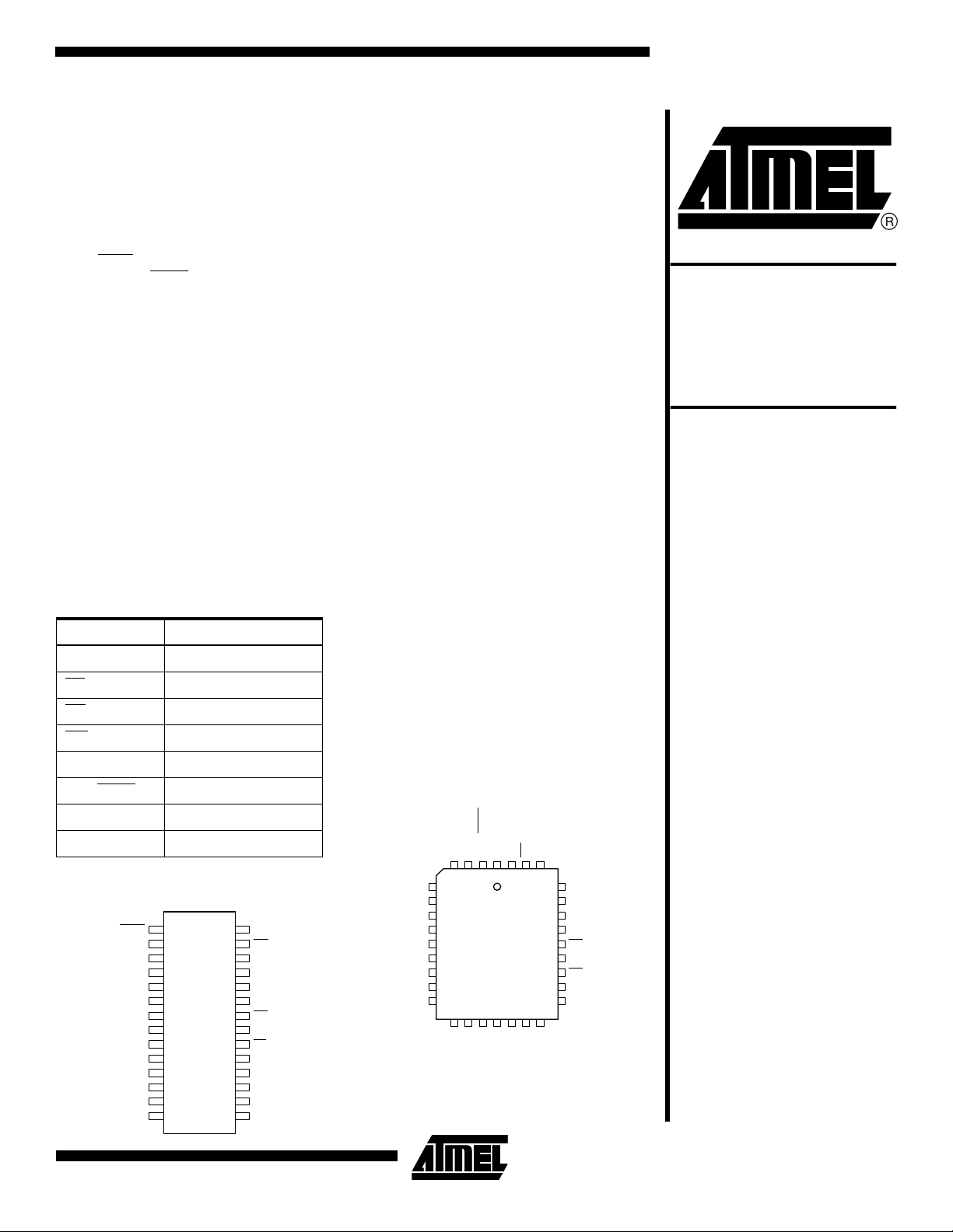
Pin Configurations
Pin Name Function
A0 - A10 Addresses
CE
OE
WE Write Enable
I/O0 - I/O7 Data Inputs/Outputs
RDY/BUSY
NC No Connect
DC Don’t Connect
RDY/BUSY
I/O0
I/O1
I/O2
GND
Chip Enable
Output Enable
Ready/Busy Output
PDIP, SOIC
Top Vie w
1
2
NC
3
A7
4
A6
5
A5
6
A4
7
A3
8
A2
9
A1
10
A0
11
12
13
14
28
VCC
27
WE
26
NC
25
A8
24
A9
23
NC
22
OE
21
A10
20
CE
19
I/O7
18
I/O6
17
I/O5
16
I/O4
15
I/O3
PLCC
Top View
A7NCRDY/BUSYDCVCCWENC
432
1
I/O2
GND
DC
323130
I/O3
I/O4
29
28
27
26
25
24
23
22
21
I/O5
A8
A9
NC
NC
OE
A10
CE
I/O7
I/O6
NC
I/O0
5
A6
6
A5
7
A4
8
A3
9
A2
10
A1
11
A0
12
13
14151617181920
I/O1
Note: PLCC package pins 1 and 17 are
DON’T CONNECT.
Rev. 0541B–10/98
1
Page 2
The AT28C17 is accessed li k e a s tatic R AM f or the r ea d or
write cycles without the ne ed of exte rnal com ponents. During a byte write, the addr ess and data are latche d internally, freeing th e microp rocessor address and data b us for
other operations. Following the initiation of a write cycle,
the device will go to a busy state and automatically clear
and write the latched d ata usi ng an i nternal c ontrol t imer.
The device includes two methods for detecting the end of a
write cycle, level detection of RDY/BUSY
ING of I/O
. Once the end of a write cycle has been
7
and DATA POLL-
detected, a new access for a read or a write can begin.
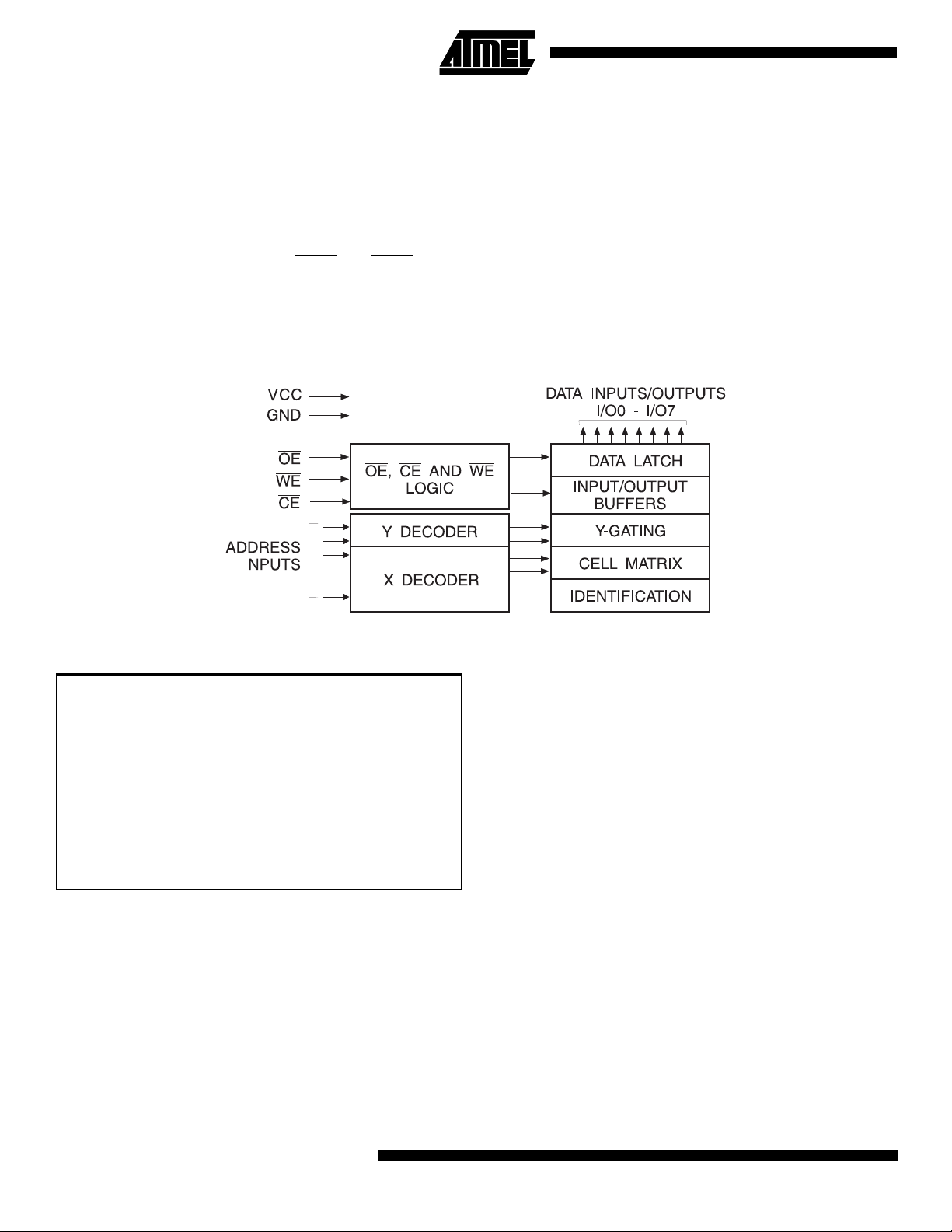
Block Diagram
The CMOS technology offers fast access times of 150 ns at
low power dissipation. When the chip is deselected the
standby current is less than 100 µA.
Atmel’s 28C17 has ad dition al featur es to e nsur e high qua lity and manufacturability. The dev ice utilizes e rror corre ction internall y for extended endurance and fo r improved
data retention character istics. An extra 32 bytes of
EEPROM are available for device identification or tracking.
Absolute Maximum Ratings*
Temperature Under Bias................................-55°C to +125°C
Storage Temperature..................................... -65°C to +150°C
All Input Voltages (including NC Pins)
with Respect to Ground...................................-0.6V to +6.25V
All Output Voltages
with Respect to Ground.............................-0.6V to VCC + 0.6V
Voltage on OE
with Respect to Ground...................................-0.6V to +13.5V
and A9
*NOTICE: Stresses beyond those listed under “Absolute
Maximum Ratings” may cause permanent damage to the de vic e. T his is a stres s r ating o nly an d
functional opera tion of the device at these or an y
other conditions beyond those indicated in the
operational sections of this specifi c ation is not
implied. Exposure to absolute maximum rating
conditions for extended periods may affect
device reli abi li ty
2
AT28C17
Page 3

Device Operation
READ:
When CE
at the memory location determined by the address pins is
asserted on the outputs. The outputs are put in a high
impedance state whenever CE
control gives designers increased flexibility in preventing
bus contention.
BYTE WRITE:
writing into a Static RAM. A low pulse on the WE
input with OE high and CE or WE low (respectively) initiates a byte write. T he address locatio n is latche d on the
last falling ed ge of WE
the first rising edge. Internally, the device performs a selfclear before write. Once a byte write has been started, it
will automatically time itself to completion. Once a programming operation has been in itiate d and for the du ratio n
of t
tion.
FAST BYTE WRITE:
time of 200 µs maximum. This feature allows the entire
device to be rewritten in 0.4 seconds.
READY/BUSY
put that can be used to detect the end of a write cycle.
RDY/BUSY
is released at the completion of the write. The open dr ain
The AT28C17 is accessed like a Stati c RAM.
and OE are low and WE is high, the data stored
or OE is high. This dual line
Writing data into the AT28C17 is similar to
(or CE); the new data i s latche d on
, a read operation will effectively be a polling opera-
WC
The AT28C17E offers a byte write
:
Pin 1 is an open drain READY/BUSY
is actively pulled low during the write cycle and
or CE
out-
AT28C17
connection allo ws for OR-tyi ng of sev eral device s to the
same RDY/BUSY
DATA
POLLING:
to signal the completion of a write cycle. During a write
cycle, an attempted read of the data being written results in
the complement of that data for I/O
indeterminate). When the write cycle is finished, true data
appears on all outputs.
WRITE PROTECTION:
are protected against in the following ways: (a) V
sense—if VCC is below 3.8V (typical) the write function is
inhibited; (b) V
3.8V the device will automatically time out 5 ms (typical)
before allowing a byte write; and (c) write inhi bit—holding
any one of OE
cycles.
CHIP CLEAR:
AT28C17 may be set to the high state by the CHIP CLEAR
operation. By setting CE
cleared when a 10 msec low pulse is applied to WE
DEVICE IDENTIFICATION:
EEPROM memory are available to the user for device identification. By raising A9 to 12 ± 0.5V and using address
locations 7E0H to 7FFH the additional bytes may be written
to or read from in th e s am e m ann er a s the regul ar m emo ry
array.
line.
The AT28C17 provides DATA
(the other outputs are
7
Inadvertent writes to the devi ce
power on delay once VCC has reached
CC
low, CE high or WE high inhibits byte write
The contents of the entire memory of the
low and OE to 12 volts, the chip is
An extra 32 bytes of
POLLING
CC
.
3
Page 4
DC and AC Operating Range
AT28C17-15
Operating
Temperature (Case)
V
Power Supply 5V ± 10%
CC
Com. 0°C - 70°C
Ind. -40°C - 85°C
Operating Modes
Mode CE OE WE I/O
Read V
(2)
Write
Standby/Write Inhibit V
IL
V
IL
IH
Write Inhibit X X V
Write Inhibit X V
Output Disable X V
Chip Erase V
IL
V
X
V
IL
V
IH
(1)
IL
IH
(3)
H
V
IH
V
IL
D
OUT
D
IN
XHigh Z
IH
X
XHigh Z
VIL High Z
Notes: 1. X can be VIL or VIH.
2. Refer to AC Programming Waveforms.
= 12.0V ± 0.5V.
3. V
H
DC Characteristics
Symbol Parameter Condition Min Max Units
I
I
I
I
LI
LO
SB1
SB2
Input Load Current VIN = 0V to VCC + 1V 10 µA
Output Leakage Current V
VCC Standby Current CMOS CE = V
= 0V to V
I/O
CC
CC
10 µA
- 0.3V to VCC + 1.0V 100 µA
Com. 2 mA
VCC Standby Current TTL CE = 2.0V to VCC + 1.0V
Ind. 3 mA
I
CC
V
IL
V
IH
V
OL
V
OH
4
V
Active Current AC
CC
Input Low Voltage 0.8 V
Input High Voltage 2.0 V
Output Low Voltage
Output High Voltage IOH = -400 µA2.4V
AT28C17
f = 5 MHz; I
CE
= V
IL
= 2.1 mA
I
OL
= 4.0 for RDY/BUSY
OUT
= 0 mA
Com. 30 mA
Ind. 45 mA
.4 V
Page 5

AC Read Characteristics
Symbol Parameter
t
ACC
(1)
t
CE
(2)
t
OE
(3)(4)
t
DF
t
OH
AC Read Waveforms
Address to Output Delay 150 ns
CE to Output Delay 150 ns
OE to Output Delay 10 70 ns
CE or OE High to Output Float 0 50 ns
Output Hold from OE, CE or Address, whichever occurred first 0 ns
(1)(2)(3)(4)
AT28C17
AT28C17-15
UnitsMin Max
Notes: 1. CE may be delayed up to t
2. OE may be delayed up to tCE - tOE after the falling edge of CE with out im pa ct on tCE or by t
without impact on t
ACC
.
- tCE after the address transition without impact on t
ACC
ACC
.
- tOE after an address change
ACC
3. tDF is specified from OE or CE whichever occurs first (CL = 5 pF).
4. This parameter is characterized and is not 100% tested.
Input Test Waveforms and
Output Test Load
Measurement Level
tR, tF < 20 ns
Pin Capacitance
f = 1 MHz, T = 25°C
Symbol Ty p Max Units Conditions
C
IN
C
OUT
Note: 1. This parameter is characterized and is not 100% tested.
(1)
46pFV
812pFV
IN
OUT
= 0V
= 0V
5
Page 6

AC Write Characteristics
Symbol Parameter Min Typ Max Units
tAS, t
t
AH
t
WP
t
DS
t
DH
t
CS
t
DB
OES
, t
OEH
, t
CH
Address, OE Set-up Time 10 ns
Address Hold Time 50 ns
Write Pulse Width (WE or CE) 100 1000 ns
Data Set-up Time 50 ns
Data, OE Hold Time 10 ns
CE to WE and WE to CE Set-up and Hold Time 0 ns
Time to Device Busy 50 ns
AT28C17 0.5 1.0 ms
t
WC
Write Cycle Time
AT28C17E 100 200 µs
AC Write Waveforms
WE Controlled
CE Controlled
6
AT28C17
Page 7

AT28C17
Data Po lling Characteristics
Symbol Parameter Min Typ Max Units
t
DH
t
OEH
t
OE
t
WR
Notes: 1. These parameters are characterized and not 100% tested.
Data Hold Time 10 ns
OE Hold Time 10 ns
OE to Output Delay
Write Recovery Time 0 ns
2. See AC Read Characteristics.
(2)
(1)
Data Polling Waveforms
ns
Chip Erase Waveforms
tS = tH = 1 µsec (min.)
tW = 10 msec (min.)
VH = 12.0 ± 0.5V
7
Page 8

8
AT28C17
Page 9

AT28C17
Ordering Information
I
t
ACC
(ns)
150 30 0.1 AT28C17(E)-15JC
Notes: 1. See Valid Part Numbers table below.
2. The 28C17 200 ns and 250 ns speed selections have been removed from valid selections table and are replaced by the
faster 150 ns T
3. The 28C17 ceramic and LCC package offerings have been removed. New designs should utilize the 28C256 ceramic offerings.
(mA)
CC
45 0.1 AT28C17(E)-15JI
AA
(1)
Ordering Code Package Operation RangeActive Standby
AT28C17(E)-1 5PC
AT28C17(E)-1 5SC
AT28C17(E)-15PI
AT28C17(E)-15SI
offering.
Valid Part Numb ers
The following table lists standard Atmel products that can be ordered.
Device Numbers Speed Package and Temperature Combinations
AT28C17 15 JC, JI, PC, PI, SC, SI
AT28C17E 15 JC, JI, PC, PI, SC, SI
32J
28P6
28S
32J
28P6
28S
Commercial
(0°C to 70°C)
Industrial
(-40°C to 85°C)
AT28C17 -W
Die Products
Reference Section: Parallel EEPROM Die Products
Package Type
32J 32-Lead, Plastic J-Leaded Chip Carrier (PLCC)
28P6 28-Lead, 0.600" Wide, Plastic Dull Inline Package (PDIP)
28S 28-Lead, 0.300" Wide, Plastic Gull Wing, Small Outline (SOIC)
W Die
Options
Blank Standard Device: Endurance = 10K Write Cycles; Write Time = 1 ms
E High Endurance Option: Endurance = 100K Write Cycles; Write Time = 200 µs
9
Page 10

Packaging Information
32J
, 32-Lead, Plastic J-Leaded Chip Carrier (PLCC)
Dimensions in Inches and (Millimeters)
JEDEC STANDARD MS-018 AA
.045(1.14) X 45°
.032(.813)
.026(.660)
.050(1.27) TYP
PIN NO.1
IDENTIFY
.553(14.0)
.547(13.9)
.300(7.62) REF
.430(10.9)
.390(9.90)
AT CONTACT
POINTS
.453(11.5)
.447(11.4)
.495(12.6)
.485(12.3)
.025(.635) X 30° - 45°
.595(15.1)
.585(14.9)
.022(.559) X 45° MAX (3X)
.012(.305)
.008(.203)
.530(13.5)
.490(12.4)
.021(.533)
.013(.330)
.030(.762)
.015(3.81)
.095(2.41)
.060(1.52)
.140(3.56)
.120(3.05)
28P6
, 28-Lead, 0.600" Wide, Plastic Dual Inline
Package (PDIP)
Dimensions in Inches and (Millimeters)
JEDEC STANDARD MS-011 AB
1.47(37.3)
.220(5.59)
SEATING
PLANE
.161(4.09)
.125(3.18)
MAX
.110(2.79)
.090(2.29)
.012(.305)
.008(.203)
1.44(36.6)
1.300(33.02) REF
.065(1.65)
.041(1.04)
.630(16.0)
.590(15.0)
.690(17.5)
.610(15.5)
PIN
0
REF
15
1
.566(14.4)
.530(13.5)
.090(2.29)
.005(.127)
.065(1.65)
.015(.381)
.022(.559)
.014(.356)
MAX
MIN
28S
, 24-Lead, 0.300" Wide, Plastic Gull Wing Small
Outline (SOIC)
Dimensions in Inches and (Millimeters)
10
AT28C17
Page 11

AT28C17
11
Page 12

Atmel Headquarters Atmel Operations
Corporate Headquarters
2325 Orchard Parkway
San Jose, CA 95131
TEL (408) 441- 0311
FAX (408) 487-2600
Europe
Atmel U.K., Ltd.
Coliseum Business Centre
Riverside Way
Camberley, Surrey GU15 3YL
England
TEL (44) 1276-686677
FAX (44) 1276-686697
Asia
Atmel Asia, Ltd.
Room 1219
Chinachem Golden Plaza
77 Mody Road
Tsimshatsui East
Kowloon, Hong Kong
TEL (852) 27219778
FAX (852) 27221369
Japan
Atmel Japan K.K.
Tonetsu Shinkawa Bldg., 9F
1-24-8 Shinka wa
Chuo-ku, Tokyo 104-0033
Japan
TEL (81) 3-3523-3551
FAX (81) 3-3523-7581
Atmel Colorado Springs
1150 E. Cheyenne Mtn. Blvd.
Colorado Springs, CO 80906
TEL (719) 576-3300
FAX (719) 540-1759
Atmel Rousset
Zone Indu strie lle
13106 Rousset Cedex, France
TEL (33) 4 42 53 60 00
FAX (33) 4 42 53 60 01
Fax-on-Demand
North America:
1-(800) 292-8635
International:
1-(408) 441-0732
e-mail
literature@atmel.com
Web Site
http://www.atmel.com
BBS
1-(408) 436-4309
© Atmel Corporation 1998.
Atmel Corporation makes no warranty for the use of its products, other than those expressly contained in the Company’s standard warranty which is detailed in Atmel’s Terms and Conditions located on the Company’s website. The Company assumes no responsibility for
any errors which may appear in this document, reserves the right to change devices or specifications detailed herein at any time without
notice, and does not make any commitment to update the information contained herein. No licenses to patents or other intellectual property of Atmel are granted by the Company in connection with the sale of Atmel products, expressly or by implication. Atmel’s products are
not authorized for use as critical components in life support devices or systems.
®
Marks bearing
Terms and product names in this document may be trademarks of others.
and/or ™ are registered trademarks and trademarks of Atmel Corporation.
Printed on recycled paper.
0541B–10/98/xM
 Loading...